Advances in Tracking Detectors Frank Hartmann KIT Karlsruhe Institute of Technology Institut für Experimentelle Kernphysik Hermann-von-Helmholtz-Platz 1 76344 Eggenstein-Leopoldshafen Germany [email protected]Jochen Kaminski Rheinische Friedrich-Wilhelms-Universität Bonn Physikalisches Institut Nußallee 12 53115 Bonn Germany [email protected]Key Words: Silicon sensor, gaseous detector, radiation hardness, active pixels Abstract: Tracking detectors are of vital importance for most experiments in high energy and nuclear physics. They are used to determine the charge, momentum and energy of traversing particles and to allow quark flavor identification through reconstruction of secondary vertices. The main two families are gaseous and semiconductor detectors, while more exotic ones are fiber or transition radiation tracking (TRT) devices. The starting points were cloud and bubble chambers in the 1950s and wire chambers in the 1970s which still dominated the field in the 1980s when silicon sensors appeared on the scene. Today, silicon strip- and pixel sensors, time projection chambers (TPC), gas electron multiplier (GEM) and MICROMEGAS define the field. The more advanced detector types will be elaborated in this review emphasizing application examples and future plans.
Transcript
Advances in Tracking Detectors
Frank Hartmann
KIT Karlsruhe Institute of Technology Institut für Experimentelle Kernphysik Hermann-von-Helmholtz-Platz 1 76344 Eggenstein-Leopoldshafen
Key Words: Silicon sensor, gaseous detector, radiation hardness, active pixels
Abstract: Tracking detectors are of vital importance for most experiments in high energy and nuclear physics. They are used to determine the charge, momentum and energy of traversing particles and to allow quark flavor identification through reconstruction of secondary vertices. The main two families are gaseous and semiconductor detectors, while more exotic ones are fiber or transition radiation tracking (TRT) devices. The starting points were cloud and bubble chambers in the 1950s and wire chambers in the 1970s which still dominated the field in the 1980s when silicon sensors appeared on the scene. Today, silicon strip- and pixel sensors, time projection chambers (TPC), gas electron multiplier (GEM) and MICROMEGAS define the field. The more advanced detector types will be elaborated in this review emphasizing application examples and future plans.
leszek
Typewritten Text
To be published in: Annual Review of Nuclear and Particle Science Vol. 61
leszek
Typewritten Text
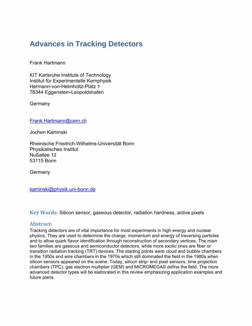
1.) Introduction to Silicon Strip Sensors The first usage of silicon for precision tracking was demonstrated in the late 70’s in the NA11 (1) fixed target experiment where the planar technology was introduced (2). In the last decades, there were several silicon detector milestones: the high precision SLD VXD detector (3), a tin can worth of Charged Coupled Devices (CCD) at SLAC or the silicon strip vertex detectors at the Large Electron Positron Collider (LEP), where double-sided silicon sensors were already complemented by forward pixels in DELPHI (4; 5). The SVX (6; 7; 8) tracking detector inside CDF at Fermi National Accelerator Laboratory was the first silicon position sensitive detector in a hadron collider environment. Today ATLAS (9) and CMS (10) at the Large Hadron Collider (LHC) (11) at CERN (12) and FERMI (13) a satellite experiment include the largest operating detectors. The evolution of these devices can be seen in Figure 1.
Figure 1
Picture of an NA11 sensor plane, an inner view of the DELPHI Micro Vertex Detector of 1994, the CDF Intermediate Silicon Layers detector of Run II and the packed CMS tracker next to the OPAL one (upper left to lower right). Active area increased from 10-2
to 100
to 101 to 2x10² m2 [Courtesy CERN, FNAL]
At present the most common silicon tracking sensors are fully depleted strip and pixel sensors. Strip devices consist of ~100 to 500 µm thick silicon (n- or p-bulk) slices where at least one face is segmented by lithography technology with differently doped strip implants (electrodes) to form discrete pn-junctions (planar technology (14)). A reverse bias voltage is applied to the pn-junctions to fully deplete the volume from free charge carriers and to establish a linear field from
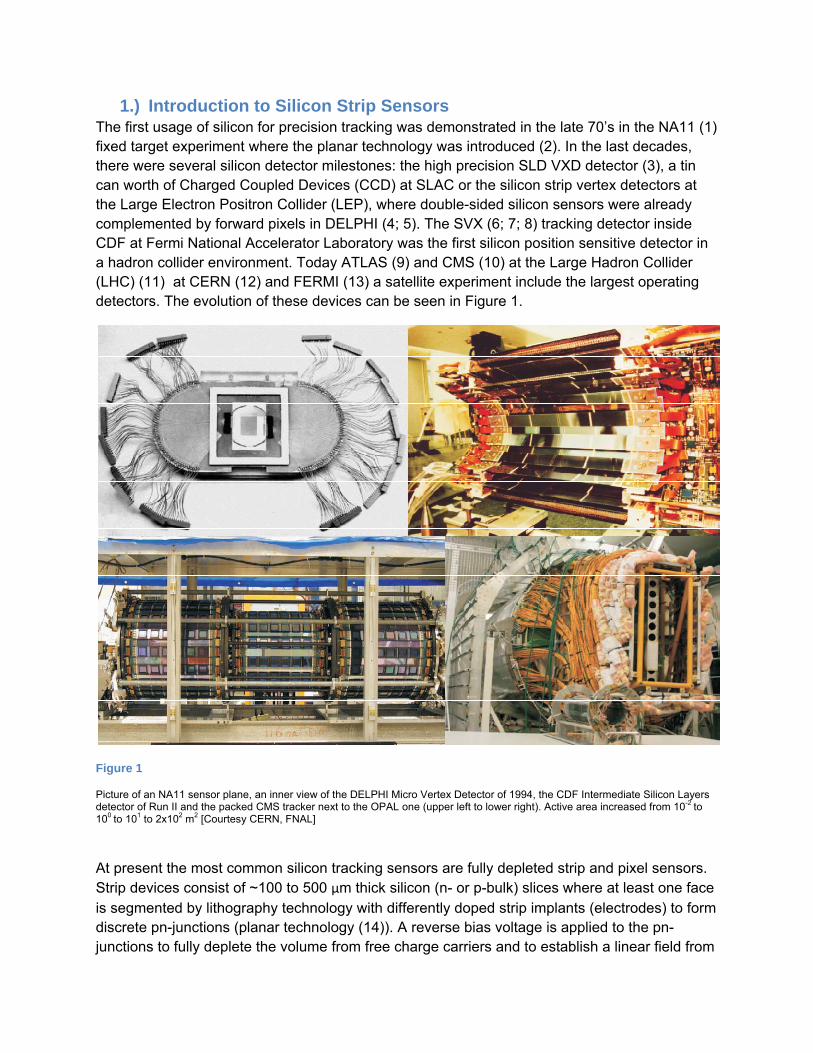
back to front. A schematic and a corresponding photo of a real strip device are depicted in Figure 2. More sophisticated detectors also segment the second face with a small stereo or full 90° angle different strip orientation – channel routing is realized on top of an additional isolation layer (15; 16).
Precison marker
Str
ip n
umb
er
AC Pad
DCPad
Biasresistor
Bia
srin
g
Gu
ard
ring
Outer protecting ring(for CMS: AL on n++)
SiO
2 c
ove
ring
Si
Figure 2
The 3D schematic of a single-sided AC-coupled, Rpoly biased sensor shows the baseline of the CMS sensor at the LHC. In operation, the bias ring is connected to GND potential, which is then distributed via the polysilicon bias resistors to the p+ implant strips, while the Al backplane is set to positive high voltage depleting the full n-bulk volume of free charge carriers by forming a pn-junction p+ strip to n-bulk. The long strips and thin decoupling oxide allows for high coupling capacitances implanted directly in the sensor. The guard ring shapes the field at the borders. The n++ ring defines the active volume and prevents high field in the edge regions. The photo shows a view of an actual sensor surface of a sensor with a strip pitch of 80µm.
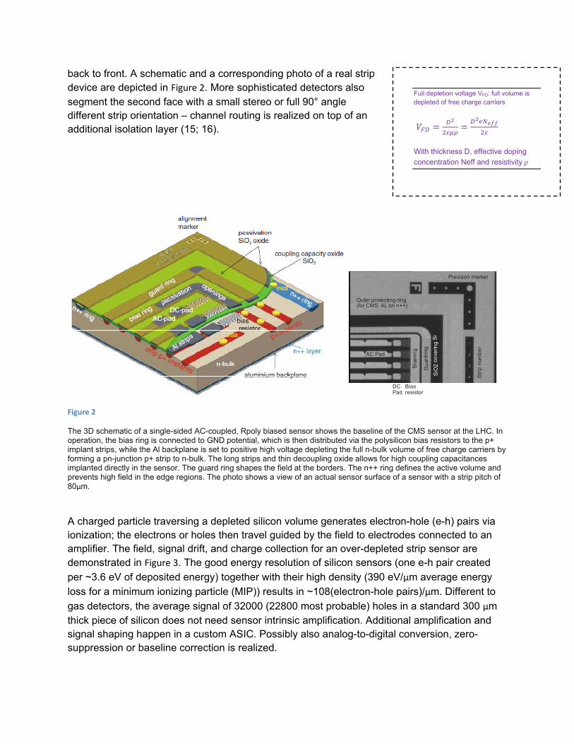
A charged particle traversing a depleted silicon volume generates electron-hole (e-h) pairs via ionization; the electrons or holes then travel guided by the field to electrodes connected to an amplifier. The field, signal drift, and charge collection for an over-depleted strip sensor are demonstrated in Figure 3. The good energy resolution of silicon sensors (one e-h pair created
per ~3.6 eV of deposited energy) together with their high density (390 eV/µm average energy
loss for a minimum ionizing particle (MIP)) results in ~108(electron-hole pairs)/µm. Different to
gas detectors, the average signal of 32000 (22800 most probable) holes in a standard 300 µm thick piece of silicon does not need sensor intrinsic amplification. Additional amplification and signal shaping happen in a custom ASIC. Possibly also analog-to-digital conversion, zero-suppression or baseline correction is realized.
Full depletion voltage VFD: full volume is depleted of free charge carriers
With thickness D, effective doping
concentration Neff and resistivity
Figure 3
The first plot shows the 2-dimensional electrical field configuration emphasizing the situation at the discrete strips, while the second illustrates the field linearity across the bulk volume, projected on a strip center. The third plot shows the field dependant mobilities of holes and electrons. In the following, an ionizing particle traverses the sensor at an angle of 45° disturbing the static situation. The rightmost plot displays the resulting charge collected at the individual strips in a time resolved way also quoting the integrated sums. In the following eight plots, one can observe the simulated time evolution of the absolute electrons and holes charge densities.
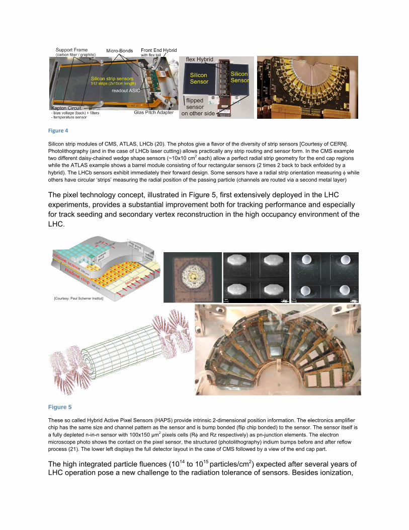
2.) Present Silicon Detectors Technology in Operation The largest silicon tracking detectors out of boutique-like double-sided sensors are CDF and D0 (17) at the TEVATRON at Fermilab – first processing on 6” wafers (18). All four experiments at the LHC operate silicon strip detectors combined with hybrid active pixel (ALICE (19), ATLAS, CMS), silicon drift (ALICE) or a TRT (ATLAS). Figure 4 shows a variety of silicon strip modules showing clearly the advances of the last decades in size (sensors) and miniaturization (electronic chips ASIC).
Figure 4
Silicon strip modules of CMS, ATLAS, LHCb (20). The photos give a flavor of the diversity of strip sensors [Courtesy of CERN]. Photolithography (and in the case of LHCb laser cutting) allows practically any strip routing and sensor form. In the CMS example two different daisy-chained wedge shape sensors (~10x10 cm2 each) allow a perfect radial strip geometry for the end cap regions while the ATLAS example shows a barrel module consisting of four rectangular sensors (2 times 2 back to back enfolded by a hybrid). The LHCb sensors exhibit immediately their forward design. Some sensors have a radial strip orientation measuring while others have circular ‘strips’ measuring the radial position of the passing particle (channels are routed via a second metal layer)
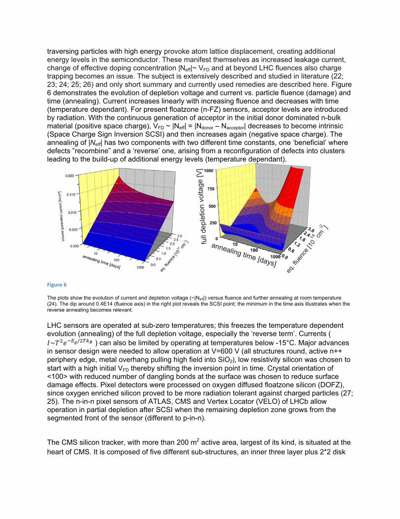
The pixel technology concept, illustrated in Figure 5, first extensively deployed in the LHC experiments, provides a substantial improvement both for tracking performance and especially for track seeding and secondary vertex reconstruction in the high occupancy environment of the LHC.
[Courtesy: Paul Scherrer Institut]
Figure 5
These so called Hybrid Active Pixel Sensors (HAPS) provide intrinsic 2-dimensional position information. The electronics amplifier chip has the same size and channel pattern as the sensor and is bump bonded (flip chip bonded) to the sensor. The sensor itself is a fully depleted n-in-n sensor with 100x150 µm2 pixels cells (R and Rz respectively) as pn-junction elements. The electron microscope photo shows the contact on the pixel sensor, the structured (photolithography) indium bumps before and after reflow process (21). The lower left displays the full detector layout in the case of CMS followed by a view of the end cap part.
The high integrated particle fluences (1014 to 1015 particles/cm2) expected after several years of LHC operation pose a new challenge to the radiation tolerance of sensors. Besides ionization,
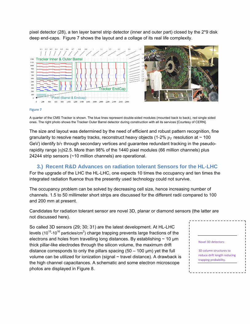
traversing particles with high energy provoke atom lattice displacement, creating additional energy levels in the semiconductor. These manifest themselves as increased leakage current, change of effective doping concentration |Neff|~ VFD and at beyond LHC fluences also charge trapping becomes an issue. The subject is extensively described and studied in literature (22; 23; 24; 25; 26) and only short summary and currently used remedies are described here. Figure 6 demonstrates the evolution of depletion voltage and current vs. particle fluence (damage) and time (annealing). Current increases linearly with increasing fluence and decreases with time (temperature dependant). For present floatzone (n-FZ) sensors, acceptor levels are introduced by radiation. With the continuous generation of acceptor in the initial donor dominated n-bulk material (positive space charge), VFD ~ |Neff| = |Ndonor – Nacceptor| decreases to become intrinsic (Space Charge Sign Inversion SCSI) and then increases again (negative space charge). The annealing of |Neff| has two components with two different time constants, one ‘beneficial’ where defects ”recombine” and a ‘reverse’ one, arising from a reconfiguration of defects into clusters leading to the build-up of additional energy levels (temperature dependant).
Figure 6
The plots show the evolution of current and depletion voltage (~|Neff|) versus fluence and further annealing at room temperature (24). The dip around 0.4E14 (fluence axis) in the right plot reveals the SCSI point; the minimum in the time axis illustrates when the reverse annealing becomes relevant.
LHC sensors are operated at sub-zero temperatures; this freezes the temperature dependent evolution (annealing) of the full depletion voltage, especially the ‘reverse term’. Currents ( ~ / ) can also be limited by operating at temperatures below -15°C. Major advances
in sensor design were needed to allow operation at V=600 V (all structures round, active n++ periphery edge, metal overhang pulling high field into SiO2), low resistivity silicon was chosen to start with a high initial VFD thereby shifting the inversion point in time. Crystal orientation of <100> with reduced number of dangling bonds at the surface was chosen to reduce surface damage effects. Pixel detectors were processed on oxygen diffused floatzone silicon (DOFZ), since oxygen enriched silicon proved to be more radiation tolerant against charged particles (27; 25). The n-in-n pixel sensors of ATLAS, CMS and Vertex Locator (VELO) of LHCb allow operation in partial depletion after SCSI when the remaining depletion zone grows from the segmented front of the sensor (different to p-in-n).
The CMS silicon tracker, with more than 200 m2 active area, largest of its kind, is situated at the heart of CMS. It is composed of five different sub-structures, an inner three layer plus 2*2 disk
pixel detector (28), a ten layer barrel strip detector (inner and outer part) closed by the 2*9 disk deep end-caps. Figure 7 shows the layout and a collage of its real life complexity.
11..11mm
Figure 7
A quarter of the CMS Tracker is shown. The blue lines represent double-sided modules (mounted back to back), red single sided ones. The right photo shows the Tracker Outer Barrel detector during construction with all its services [Courtesy of CERN].
The size and layout was determined by the need of efficient and robust pattern recognition, fine granularity to resolve nearby tracks, reconstruct heavy objects (1-2% resolution at ~ 100
GeV) identify b/ through secondary vertices and guarantee redundant tracking in the pseudo-
rapidity range ||≤2.5. More than 98% of the 1440 pixel modules (66 million channels) plus 24244 strip sensors (~10 million channels) are operational.
3.) Recent R&D Advances on radiation tolerant Sensors for the HL-LHC For the upgrade of the LHC the HL-LHC, one expects 10 times the occupancy and ten times the integrated radiation fluence thus the presently used technology could not survive.
The occupancy problem can be solved by decreasing cell size, hence increasing number of channels. 1.5 to 50 millimeter short strips are discussed for the different radii compared to 100 and 200 mm at present.
Candidates for radiation tolerant sensor are novel 3D, planar or diamond sensors (the latter are not discussed here).
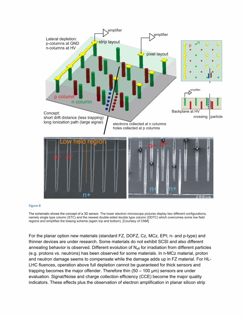
So called 3D sensors (29; 30; 31) are the latest development. At HL-LHC levels (1015-1016 particles/cm2) charge trapping prevents large fractions of the electrons and holes from travelling long distances. By establishing ~ 10 µm thick pillar-like electrodes through the silicon volume, the maximum drift distance corresponds to only the pillars spacing (50 – 100 µm) yet the full volume can be utilized for ionization (signal ~ travel distance). A drawback is the high channel capacitances. A schematic and some electron microscope photos are displayed in Figure 8.
Novel 3D detectors:
3D column structures to
reduce drift length reducing
trapping probability.
Figure 8
The schematic shows the concept of a 3D sensor. The lower electron microscope pictures display two different configurations, namely single type column (STC) and the newest double-sided double type column (DDTC) which overcomes some low field regions and simplifies the biasing scheme (again top and bottom). [Courtesy of CNM]
For the planar option new materials (standard FZ, DOFZ, Cz, MCz, EPI; n- and p-type) and thinner devices are under research. Some materials do not exhibit SCSI and also different annealing behavior is observed. Different evolution of Neff for irradiation from different particles (e.g. protons vs. neutrons) has been observed for some materials. In n-MCz material, proton and neutron damage seems to compensate while the damage adds up in FZ material. For HL-LHC fluences, operation above full depletion cannot be guaranteed for thick sensors and trapping becomes the major offender. Therefore thin (50 – 100 µm) sensors are under evaluation. Signal/Noise and charge collection efficiency (CCE) become the major quality indicators. These effects plus the observation of electron amplification in planar silicon strip
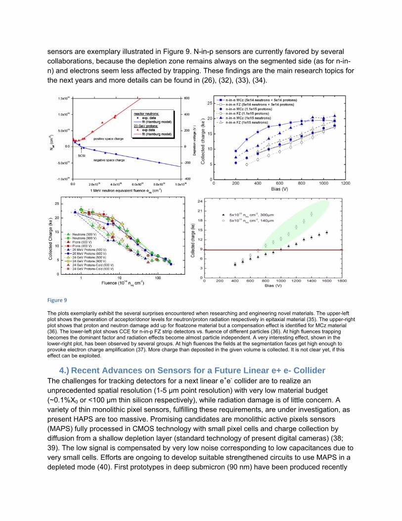
sensors are exemplary illustrated in Figure 9. N-in-p sensors are currently favored by several collaborations, because the depletion zone remains always on the segmented side (as for n-in-n) and electrons seem less affected by trapping. These findings are the main research topics for the next years and more details can be found in (26), (32), (33), (34).
Figure 9
The plots exemplarily exhibit the several surprises encountered when researching and engineering novel materials. The upper-left plot shows the generation of acceptor/donor levels for neutron/proton radiation respectively in epitaxial material (35). The upper-right plot shows that proton and neutron damage add up for floatzone material but a compensation effect is identified for MCz material (36). The lower-left plot shows CCE for n-in-p FZ strip detectors vs. fluence of different particles (36). At high fluences trapping becomes the dominant factor and radiation effects become almost particle independent. A very interesting effect, shown in the lower-right plot, has been observed by several groups. At high fluences the fields at the segmentation faces get high enough to provoke electron charge amplification (37). More charge than deposited in the given volume is collected. It is not clear yet, if this effect can be exploited.
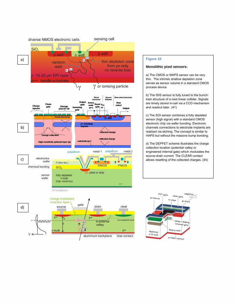
4.) Recent Advances on Sensors for a Future Linear e+ e- Collider The challenges for tracking detectors for a next linear e+e- collider are to realize an unprecedented spatial resolution (1-5 µm point resolution) with very low material budget (~0.1%X0 or <100 µm thin silicon respectively), while radiation damage is of little concern. A variety of thin monolithic pixel sensors, fulfilling these requirements, are under investigation, as present HAPS are too massive. Promising candidates are monolithic active pixels sensors (MAPS) fully processed in CMOS technology with small pixel cells and charge collection by diffusion from a shallow depletion layer (standard technology of present digital cameras) (38; 39). The low signal is compensated by very low noise corresponding to low capacitances due to very small cells. Efforts are ongoing to develop suitable strengthened circuits to use MAPS in a depleted mode (40). First prototypes in deep submicron (90 nm) have been produced recently
to establish radiation tolerant devices to be even usable for the HL-LHC (LEPIX collaboration, private communication). An attractive development is the Image Sensor with in Situ Storage (ISIS) (41) where CCD technology, active pixel transistors and CMOS edge technology are combined in one device. A combination of a fully depleted device and CMOS technology is possible in the Silicon In Insulator (SOI) technology (42), where the low resistivity electronics wafer is chemically bonded to the fully depleted high resistivity sensor wafer. One of the remaining problems is the back-gating effect, where the depletion voltage affects the CMOS circuit’s voltages. Another promising candidate (baseline for the Belle II (43)) is the Depleted Field Effect Transistor (DEPFET) detector (14; 44) where the charges, collected at an internal gate -in a fully depleted sensor- modulate the source-drain current of the implemented FET. The intrinsic amplification, hence high signal in combination with a small cell size guarantees a superb spatial resolution.
Figure 10 demonstrates the different device schemes.
p+ pixel or strip
n+
Al backplane
fully depletedn-bulk
(high resistivity)
SiO2
n (low res.)
electronics wafer
chemical bonding
sensorwafer
PMOSNMOS
metal 1 metal 2polysilicon polysilicon
Figure 10
Monolithic pixel sensors:
a) The CMOS or MAPS sensor can be very thin. The intrinsic shallow depletion zone serves as sensor volume in a standard CMOS process device.
b) The ISIS sensor is fully tuned to the bunch-train structure of a next linear collider. Signals are timely stored in-cell via a CCD mechanism and readout later. (41)
c) The SOI sensor combines a fully depleted sensor (high signal) with a standard CMOS electronic chip via wafer bonding. Electronic channels connections to electrode implants are realized via etching. The concept is similar to HAPS but without the massive bump bonding.
d) The DEPFET scheme illustrates the charge collection location (potential valley or engineered internal gate) which modulates the source-drain current. The CLEAR contact allows resetting of the collected charges. (44)
b)
a)
c)
d)
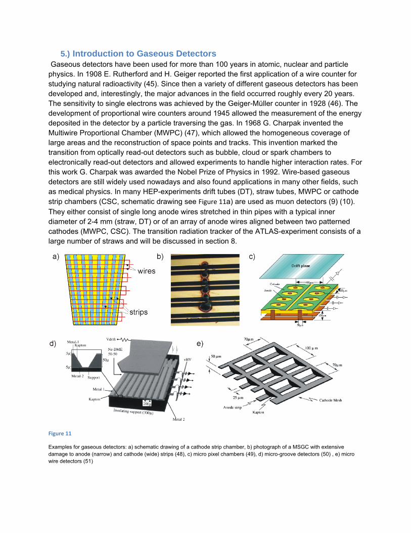
5.) Introduction to Gaseous Detectors Gaseous detectors have been used for more than 100 years in atomic, nuclear and particle physics. In 1908 E. Rutherford and H. Geiger reported the first application of a wire counter for studying natural radioactivity (45). Since then a variety of different gaseous detectors has been developed and, interestingly, the major advances in the field occurred roughly every 20 years. The sensitivity to single electrons was achieved by the Geiger-Müller counter in 1928 (46). The development of proportional wire counters around 1945 allowed the measurement of the energy deposited in the detector by a particle traversing the gas. In 1968 G. Charpak invented the Multiwire Proportional Chamber (MWPC) (47), which allowed the homogeneous coverage of large areas and the reconstruction of space points and tracks. This invention marked the transition from optically read-out detectors such as bubble, cloud or spark chambers to electronically read-out detectors and allowed experiments to handle higher interaction rates. For this work G. Charpak was awarded the Nobel Prize of Physics in 1992. Wire-based gaseous detectors are still widely used nowadays and also found applications in many other fields, such as medical physics. In many HEP-experiments drift tubes (DT), straw tubes, MWPC or cathode strip chambers (CSC, schematic drawing see Figure 11a) are used as muon detectors (9) (10). They either consist of single long anode wires stretched in thin pipes with a typical inner diameter of 2-4 mm (straw, DT) or of an array of anode wires aligned between two patterned cathodes (MWPC, CSC). The transition radiation tracker of the ATLAS-experiment consists of a large number of straws and will be discussed in section 8.
Figure 11
Examples for gaseous detectors: a) schematic drawing of a cathode strip chamber, b) photograph of a MSGC with extensive damage to anode (narrow) and cathode (wide) strips (48), c) micro pixel chambers (49), d) micro-groove detectors (50) , e) micro wire detectors (51)
With the continuous increase in experimental requirements, especially in rate capability, the demand for a new readout technology grew. A. Oed introduced the era of Micropattern Gaseous Detectors (MPGDs) by presenting the first results of the Microstrip Gas Chambers (MSGC) in 1988 (52). This device consisted of alternating narrow anode strips and wider cathode strips placed by photolithographic process on a high resistive carrier material. Because of the new configuration the pitch between the sensitive regions decreased from at least 1 mm down to 200 µm. Due to faster neutralization of ions by the close by cathode strips and the higher granularity of the active area the MSGCs could be operated at particle fluxes exceeding 1 MHz/mm². Also spatial resolutions of a few tens of µm could routinely be reached. The application of MSGC was, however, limited by destructive discharges, which were triggered by occasional high charge depositions close to the anode strips leading to breaks in the anode strips (Figure 11b). In
the following years, a large variety of different MPGDs were conceived and tested (Figure 11c-e): micro-gap chambers (53), small gap chambers (54), microdot chambers (55), micro pixel chambers (49), micro-groove detectors (50), micro wire detectors (51), Compteur À Trou (56). Two concepts performed well enough to be accepted by a large community: Gas Electron Multipliers (GEMs) (57) and MICROMEsh GAseous Structures (Micromegas) (58).
The fundamental working principles of gaseous detectors, such as ionization, drift, diffusion and gas amplification, have been summarized in many articles and textbooks and will not be reviewed here (see Related Sources).
6.) GEM-based Planar Detectors GEMs were invented by F. Sauli in 1996. Their first applications were limited to preamplifying stages of MWPCs and MSGCs. But soon the full potential of GEMs was realized and numerous tests based on the combination of several GEMs with micro-pattern readout boards were performed. Optimization of the GEM geometry and production procedure has resulted in a 'standard GEM' that is used in most cases. These GEMs consist of a 50 µm thick polymer insulator (Kapton) that is covered with 3 µm thick copper layers on both sides. In this sandwich structure, a hexagonal pattern of micro holes with a pitch of 140 µm is etched from both sides in a photolithographic process. Due to the simultaneous etching from both sides, the holes acquire a double conical cross section with diameters of 70 µm in the copper and 50 to 60 µm in the Kapton (Figure 12a).
Figure 12
Gas Electron Multiplier: a) SEM picture of a standard GEM (Courtesy of CERN), b) schematic drawing of electric field lines and charge flow in a GEM, c) schematic drawing of a multi-GEM planar detector, d) example track seen by a triple-GEM and 4 Timepix chips, e) Reconstructed position of charge depositions from a triple GEM-detector with Timepix readout, f) spherical GEM-detector (59)
If a voltage difference is applied between both sides a strong dipole field is formed inside the holes. Electrons drifting in the gas volume above the GEM are guided by the electrical field into the hole. Here, the strong field leads to an avalanche gas amplification increasing the number of electrons by two to three orders of magnitude. While a significant fraction of the charge is
collected by the lower electrode the remaining electrons are released in the gas volume below the GEM (Figure 12b). This configuration provides a very important merit of the GEM: the complete decoupling of the gas amplification region from the readout region. Several GEMs can be stacked at short distances (typically 1-2 mm) on top of each other distributing the gas amplification among several stages (Figure 12c). This allows a lot of flexibility in optimizing the setup for reducing the discharge probability or the amount of ions released into the drift region. A detailed study minimizing the discharge rate was performed in the context of the COMPASS-experiment (60). This experiment uses 20 GEM trackers of the size 31×31 cm² as central tracking devices close to the high intensity hadronic beam (61). In the study it was observed that a triple-GEM detector operated in a Ar:CO2 70:30 gas mixture could reach a discharge probability per minimum ionizing particle of less than 10-12 while providing a total gain of 104, which is sufficient for a detection efficiency of more than 97 % (62). Based on the good results during the data taking of the COMPASS-experiment, the TOTEM-experiment (63) at the LHC opted for semi-circular shaped detectors with very similar structure and performance (64).
Another important aspect for the detector development is the detector performance with respect to spatial and time resolution. Because of the decoupling of the gas amplification and the charge collection, the readout geometry can be chosen freely, for example 2 perpendicular strips (60), rectangular, chevron or rhombus shaped pads (65) and highly pixelized readouts (66) (67). The spatial resolution reached with the various geometries scales with their feature sizes and is often reported to be below 100 µm (60) (68). If a readout with very small pixel sizes such as the Timepix chip (69) with its 55×55 µm² pixels is used in combination with a triple-GEM, one can identify and reconstruct the amplified charge depositions originating from single primary electrons (example track shown in Figure 12d). Figure 12e shows the distribution of the charge distributions in the readout plane. The accumulation pattern with a pitch of 140 µm indicates that the resolution is only limited by the pitch of the GEM holes (70).
The signal in a GEM detector is generated only by the electrons drifting from the last GEM to the readout plane, while the ions generated do not contribute to the signal. Because of the high electron mobility in the gas, the signal therefore is much shorter than in wire chambers and the time resolution is enhanced. The triple-GEM detectors in the muon system of the LHCb-experiment reach a time resolution of 4.5-10 ns depending on the gas mixture and, therefore, the information is included in the trigger decision (68).
For the safe operation and for optimizing the detector for various applications a good understanding of the gas amplification process is necessary. Therefore, several groups have studied the charge transfer in multi-GEM structures with the help of experimental setups and computer simulations (71) (72) (73). In a fair approximation an electric flux model based on the electric field lines shows that collection efficiency of the ions and electrons into the GEM holes and the extraction efficiency out of the holes is dominated by the ratio of external fields over fields in the GEM hole. For gas mixtures with high diffusion coefficients, the flux model has only limited predictive power, since a significant number of electrons is additionally lost to the copper electrodes or to the insulating walls of the hole. The latter effect together with a polarization of the insulator results in a modification of the electric field in the hole and, thus, of the gas gain. This effect is called 'charge up' and its time constant and amplitude largely depend on the form
of the holes, but can be influenced by external parameters such as irradiation rate and water content of the gas mixture (74).
Strong irradiation can also lead to permanent modification of gaseous detectors. This phenomenon is known as 'aging' and mostly due to polymerization deposits close to regions of gas amplification. The effect is very sensitive to the experimental setup, in particular, to impurities in the gas mixture. However in general MPGDs have proven to be less prone to aging than wire chambers (75). Triple GEM detectors were irradiated with various amounts of charge in different studies. The highest amount so far was tested in the context of the aforementioned muon system of the LHCb-detector, where up to 230 mC were deposited on an area of 1 mm², and a signal degradation of less than 5 % was observed (68).
Planar multi-GEM detectors have been successfully used in a wide range of conditions. But a number of experiments require special detector layouts, for example a cylindrical GEM-detector as a central tracking device for the KLOE-detector at Frascati (76) or a spherical detector for parallax free detection of x-ray scattering (Figure 12f) (59). The size of GEM-detectors has been limited by the production process of the GEM foils: Both copper electrodes are covered with a photoresist. Then the masks for the holes are placed on both sides and have to be aligned within a few micrometers, which is feasible only for mask sizes up to 40×40 cm². To overcome this restriction a new production flow was designed, in which only a single mask is used to etch the hole pattern in one copper layer. Then the Kapton etching is carried out and in a final step the second copper layer is etched using the remaining sandwich as mask. These single mask GEMs perform similarly well as the 'standard GEMs' and can be produced with significantly larger areas, limited only by the dimensions of the machines and base material (77).
7.) Micromegas-based Planar Detectors Micromegas detectors are two stage parallel plate detectors and were introduced in 1996. As shown in Figure 13a a fine grained conductive mesh, supported by insulating pillars, separates the large drift region from a thin amplification region. A low electric field of typically a few hundred V/cm guides the ionization electrons in the drift region from their point of creation towards the grid. Entering the amplification region the electrons are then accelerated by a much stronger electrical field of several tens of kV/cm, which allows gas amplification. The gap is typically between 50 µm and 100 µm thick and gas gains of several thousand can be reached. As with GEM-detectors the COMPASS-experiment was the first large HEP experiment to use this kind of detectors. 12 detectors with an area of 40×40cm² each were installed in the experiment and successfully operated even at particle rates of up to 450 kHz/cm². At low rates a gas gain of 6000 proved to be sufficient to reach an efficiency of more than 98 % per detector, a spatial resolution of about 70 µm could be shown and no aging was observed (78). Previous studies had shown that the discharge probability could be reduced by choosing a gas mixture with low atomic numbers (Ne:C2H6:CF4 80:10:10) and lower gas gain. Therefore, the gas gain was lowered down to 3000 during data taking with high intensity hadronic beam. Thereby, the performance of the detector degraded only marginally, but the discharge rate did not exceed 0.1
discharges/s. Special protection circuits could protect the readout electronics efficiently from damage (79).
Figure 13
Micromegas detector: a) schematic drawing of a Micromegas detector, b) production process of ‘bulk-Micromegas’, c) production process of ‘microbulk-Micromegas’, d) example track seen by an InGrid detector (Courtesy of NIKHEF), e) schematic drawing of a detector with a resistive layer on the readout pads and signal development on the pads, f) spatial resolution in dependence on the drift distance in high magnetic fields (80)
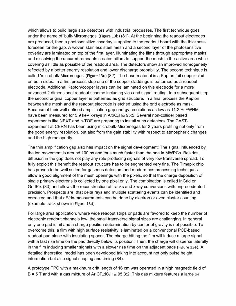
For good results, the amplification gap has to be kept constant with a very high precision. First Micromegas detectors used quartz fibers and even fishing lines as pillars on which the mesh was mounted. Recent years have seen a significant improvement in the production technique
which allows to build large size detectors with industrial processes. The first technique goes under the name of 'bulk-Micromegas' (Figure 13b) (81). At the beginning the readout electrodes are produced, then a photosensitive coverlay is applied to the readout board with the thickness foreseen for the gap. A woven stainless steel mesh and a second layer of the photosensitive coverlay are laminated on top of the first layer. Illuminating the films through appropriate masks and dissolving the uncured remnants creates pillars to support the mesh in the active area while covering as little as possible of the readout area. The detectors show an improved homogeneity reflected by a better energy resolution and lower discharge probability. The second technique is called 'microbulk-Micromegas' (Figure 13c) (82). The base-material is a Kapton foil copper-clad on both sides. In a first process step one of the copper claddings is patterned as a readout electrode. Additional Kapton/copper layers can be laminated on this electrode for a more advanced 2 dimensional readout scheme including vias and signal routing. In a subsequent step the second original copper layer is patterned as grid structure. In a final process the Kapton between the mesh and the readout electrode is etched using the grid electrode as mask. Because of their well defined amplification gap energy resolutions as low as 11.2 % FWHM have been measured for 5.9 keV x-rays in Ar:iC4H10 95:5. Several non-collider based experiments like NEXT and n-TOF are preparing to install such detectors. The CAST-experiment at CERN has been using microbulk-Micromegas for 2 years profiting not only from the good energy resolution, but also from the gain stability with respect to atmospheric changes and the high radiopurity.
The thin amplification gap also has impact on the signal development: The signal influenced by the ion movement is around 100 ns and thus much faster than the one in MWPCs. Besides, diffusion in the gap does not play any role producing signals of very low transverse spread. To fully exploit this benefit the readout structure has to be segmented very fine. The Timepix chip has proven to be well suited for gaseous detectors and modern postprocessing techniques allow a good alignment of the mesh openings with the pixels, so that the charge deposition of single primary electrons is collected by one pixel only. The combination is called InGrid or GridPix (83) and allows the reconstruction of tracks and x-ray conversions with unprecedented precision. Prospects are, that delta rays and multiple scattering events can be identified and corrected and that dE/dx-measurements can be done by electron or even cluster counting (example track shown in Figure 13d).
For large area application, where wide readout strips or pads are favored to keep the number of electronic readout channels low, the small transverse signal sizes are challenging. In general only one pad is hit and a charge position determination by center of gravity is not possible. To overcome this, a film with high surface resistivity is laminated on a conventional PCB-based readout pad plane with insulating spacer. The charge hitting the film will induce a large signal with a fast rise time on the pad directly below its position. Then, the charge will disperse laterally in the film inducing smaller signals with a slower rise time on the adjacent pads (Figure 13e). A detailed theoretical model has been developed taking into account not only pulse height information but also signal shaping and timing (84).
A prototype TPC with a maximum drift length of 16 cm was operated in a high magnetic field of
B = 5 T and with a gas mixture of Ar:CF4:iC4H10 95:3:2. This gas mixture features a large
(see section 8) and therefore a large reduction of the diffusion coefficient in high magnetic fields,
simulation show down to 19 µm/√cm. In such favorable conditions a constant spatial resolution of 35 µm could be measured throughout the detector (Figure 13f) (80). The resistive film does not only improve the spatial resolution, but also reduces the discharge probability. It compensates small unevennesses, and the charge deposited on the resistive film does not vanish immediately, but reduces locally the electric field in the amplification region and, thus, effectively blocking the further development of the discharge. It was demonstrated in studies for a possible muon spectrometer upgrade of the ATLAS-experiment, that the discharge rate of 'bulk-Micromegas' detectors with a resistive layer on the readout pads is at least one order of magnitude lower than without (85).
8.) Drift Chambers (DC) and Time Projection Chambers (TPC) Drift detectors feature larger drift regions. To improve the spatial resolution, the drift time is measured and can be converted to the drift distance, if the electric field is known. A simple electric configuration is given in a straw tube detector, while jet chambers feature more advanced field configurations, where field forming wires split the gas volume in different cells (86). The Transition Radiation Tracker (TRT) of ATLAS, for example, consists of almost 300,000 of these tubes. They have a length of 37 cm and 144 cm in the end-cap and the barrel region respectively. The tubes have an inner diameter of 4 mm and are arranged, so that high-energetic tracks typically cross 35 to 40 straws. The straws are embedded in a radiator (polyethylen foam), which allows the production of transition radiation by very high relativistic particles (Figure 14a). The x-ray photons convert in the straw tubes and by measuring the total
charge collected along the track the -factor of the particle can be determined.
Figure 14
Drift chamber: a) schematic drawing of working principle of TRT, b) schematic drawing of a TPC, c) electric field lines for open and closed gate configuration in a wire-based TPC readout (87), d) event display of the ALICE TPC (88), e) dE/dx measurement of the ALICE TPC in the 2010 pp run (Courtesy of CERN), f) ion backdrift of a triple GEM-stack in dependence on magnetic field (89)
The drift region of a Time Projection Chamber (TPC) (90) can reach distances of more than 2 m. A very homogeneous electrical field is applied to the gaseous volume. Electrons created through ionization by a charged particle passing through the sensitive volume drift towards the end-caps, where they are amplified and read-out. As shown in Figure 14b a 2D picture is formed on the end-cap. The drift distance of individual ionization charges can be determined using the known drift velocity and the measured drift time. The TPC features several advantages in comparison to other detector types: It is a truly three dimensional detector in which tracks can be reconstructed without any ambiguity; consisting only of gas it has a very low material budget, which is in addition evenly distributed throughout the volume; large numbers of 3D-points can be measured making not only the track reconstruction robust against high backgrounds but also facilitates particle identification based on dE/dx measurements. Often a solenoidal magnetic
field is applied (anti-) parallel to the electric field to measure the transverse momentum of particles passing through the gas volume. The magnetic field also improves the transverse spatial resolution, since it reduces the transverse diffusion coefficient by
0 / 1 ² ², where is the cyclotron frequency and the mean time between collisions of drifting electrons with gas molecules. The two major drawbacks of TPCs are the long readout time, it takes up to 100 µs until the sensitive volume has been cleared, and the high sensitivity to space charges in the drift volume. The latter issue arises from the ions, which are produced during the primary ionization of the drift gas by the charged particles and during gas amplification in the read out detectors. Because of their low mobility they accumulate and can deflect the drifting electrons of subsequent events, distorting the images of these tracks. The main contribution would be the ions from the gas amplification, which are however in general neutralized by a gated wire grid close to the gas amplification region (Figure 14c). This grid normally stays in a closed configuration, where ions and electrons are guided to the wires and are absorbed there. Upon an external trigger the grid can be brought into an open configuration, where both charges can easily pass (87). TPCs have been operated under various experimental conditions such as heavy ion colliders, lepton colliders and rare events experiments. The latest examples for each of these categories are the ALICE-TPC, the T2K-TPC and the LC-TPC, which shall be discussed in the following. For a more complete overview on TPCs see references (91) (92).
The ALICE-TPC (93) has been optimized for tracking in the high track density environment of the Pb-Pb collisions at the LHC. During the first heavy ion run very high track multiplicity events were observed, reaching several thousand tracks per event (example shown in Figure 14d). Besides accomplishing good spatial resolution and double track resolution a great effort was made to reduce the number of ions in the drift volume. For example the pitch of the gating grid wires was reduced and the gas mixture was optimized for high ion mobility and moderate primary ionization. Therefore, Ne:CO2:N2 85.7:9.5:4.8 was chosen along with a conventional and well proven wire-based gas amplification and readout scheme, anode wires and 570,000 pads. Because of the large volume and long maximum drift length of 2.5 m, the engineering
demands are challenging. For example the temperature has to be stabilized to T=0.1°C throughout the detector for the whole data taking period. The energy deposition dE/dx per momentum is shown in Figure 14e.
The T2K-experiment (94) is a long-baseline neutrino experiment in Japan. The near detector was designed to measure the neutrino flavor content, energy spectrum and interaction rates. For the first time MPGDs were chosen in a large TPC as readout and gas amplification stage. A total of 9 m² divided in 3 independent detectors was covered with bulk-Micromegas. To
distinguish e from µ a separation of electrons and muons with more than 5 is necessary. Based on dE/dx measurements this was reached for particle momenta larger than 200 MeV/c (95).
The Linear Collider project aims for an electron positron collider with a center of mass energy between 500 GeV and 3 TeV depending on LHC results. One of the detector concepts foresees a TPC as central tracking detector (96). The stringent requirements on the detector performance
demand among other things a material budget of only 3 % of a radiation length to the outer field
cage and a momentum resolution of 1/p ~ 9×10⁻⁵/GeV. This translates to a spatial resolution of
better than 100 µm in the readout plane (r-). Many tests have been performed with small scale prototypes at various labs. For example, as shown in Figure 14f the electrical configuration of a triple GEM stack has been optimized to reduce the ion back drift down to about 0.2 % raising the possibility to omit the gating grid (89). Also the use of a GEM as ion blocking device has been studied (97). To test various readout techniques and mechanical structures, the LCTPC collaboration has constructed a lightweight field cage for a prototype setup at DESY (98). The modular end-cap allows an easy exchange of readout modules which can be tested with a 5 GeV electron test beam. First tests with different modules with bulk-Micromegas and GEM modules have been successfully performed (99) (100).
Terms/Definition/Acronyms list: ASIC: Application Specific Integrated Circuit ALICE: A Large Ion Collider Experiment at the LHC at CERN, specializing in heavy ion physics ATLAS: A Toroidal LHC ApparatuS, multipurpose detector at the LHC at CERN TEVATRON: The Proton–Antiproton Collider at Fermilab near Chicago, operating since 1983, hosting the CDF and D0 detector Belle: Belle is an experiment at the KEK B-factory (e+e- collider) in Japan. Its goal is to study the origin of CP violation. CDF: Collider Detector at Fermilab, one of the two multipurpose detectors at the TEVATRON CERN: European Organization for Nuclear Research CMS: Compact Muon Solenoid, multipurpose detector at the LHC at CERN COMPASS: COmmon Muon Proton Apparatus for Structure and Spectroscopy, a fixed target experiment at CERN Cz: Czochralski (“Cz”) growth: The silicon melt is held just a few degrees above the melting point and a single rotating crystal as seed initiates the growth at the top. The process provides a natural high oxygen content. D0: Multipurpose detector situated at the interaction point D0 at the TEVATRON DELPHI: DEtector with Lepton, Photon and Hadron Identification, one of the four multipurpose detectors at LEP DOFZ: Diffused Oxygen Floatzone material EPI: Epitaxial, silicon wafer realized through epitaxial growth (from the gas phase) FZ: Floatzone, Float Zone Crystal technique (“FZ”), where a polysilicon rod is brought into contact with a seed crystal and the rod is then locally melted with RF heating GEM: Gas Electron Multiplier, gas amplification structure consisting of holes etched into a copper plated Kapton foil HAPS: Hybrid Active Pixel Sensors - fully depleted sensor with extra-electronics bump bonded on top, first used in DELPHI at LEP HEP: High Energy Physics – Collider Physics HL-LHC: High Luminosity LHC; there is also the HE-LHC, the High Energy LHC KLOE: K LOng Experiment, experiment at the Daphne accelerator at Frascati, specialized on physics with K-mesons LEP: Large Electron Positron Collider at CERN LHC: Large Hadron Collider, proton–proton collider at CERN LHCb: One of the four LHC detectors, specialized on b physics and CP violation MAPS: Monolithic Active Pixel Sensor – active electronics elements directly embedded on top of the sensor MCz: Magnetic Czochralski; see Cz but a magnetic field smoothes the oxgyzgen concentration Micromegas: MICROMEsh GAseous Structures, gas amplification structure consisting of a fine mesh mounted with a very thin gap on the readout plane MWPC: Multi-Wire Proportional Chamber, gaseous detector with an array of sense wires MPGD: Micro-Patter Gaseous Detectors, group of gaseous detectors with feature sizes in the order of 100 µm OPAL: an Omni-Purpose Apparatus at LEP
SLD at SLAC: Stanford Linear Detector at Stanford National Accelerator Laboratory
T2K: Tokai To Kamioka, accelerator-based neutrino experiment to measure the 13 mixing angle TPC: Time Projection Chamber, gaseous tracking detector based on large drift region with homogeneous electric field
Summary Points: Silicon tracking detectors matured and more than 350 m2 are now in operation, mainly
silicon strip and hybrid active pixel sensors. In ATLAS and CMS pixels are responsible to identify the quark flavor and enable track seeding while silicon strip and transition radiation detectors provide large lever arms, thus precision momentum measurement.
The challenge of today for the HL-LHC is to develop sensors which can be operated at a ten times radiation fluence and high occupancy
For the next Linear Collider ultra-precise and ultra-low mass pixilated detectors (~0.1%X0 / layer) are to be developed.
Gaseous detectors have been the major tracking devices during the last 4 decades and are still used in most HEP experiments. New developments include trackers based on micropattern gaseous detectors and the combining trackers with radiation detectors
GEMs and Micromegas are the most used gas amplification stages for planar detectors nowadays. They show excellent spatial resolution (~30 µm), good multi-particle resolution (~500 µm) and time resolution in the ns range. Besides, they have proven capable to detect very high particle rates (~106 Hz/mm2) and less prone for aging than wire based gaseous detectors.
77. Activity of CERN and LNF groups on large area GEM detectors. Alfonsi, M. et al. 1‐3, 2010, NIM A,
Vol. 617, pp. 151‐154.
78. The 40x40 cm² gaseous microstrip detector Micromegas for the high‐luminosity COMPASS
experiment at CERN. Bernet C, et al. 1‐2, 2005, NIM A, Vol. 536, pp. 61‐69.
79. New pixelized Micromegas detector for the COMPASS experiment. Neyret D, et al. 2009, JINST, Vol.
4. P12004.
80. Development of high resolution Micro‐pattern Gas Detectors with wide readout pads. MS, Dixit.
2010, JINST, Vol. 5. P03008.
81. Micromages in a bulk. Giomataris I, et al. 2, 2006, NIM A, Vol. 560, pp. 405‐408.
82. Development and performance of Microbulk Micromegas detectors. Andriamonje S, et al. 2010,
JINST, Vol. 5. P02001.
83. An electron‐multiplying 'Micromegas' grid made in silicon wafer post‐processing technology.
Chefdeville M, et al. 2, 2006, NIM A, Vol. 556, pp. 490‐494.
84. Simulating the charge dispersion phenomena in Micro Pattern Gas Detectors with a resistive anode.
Dixit MS, et al. 2, 2006, NIM A, Vol. 566, pp. 281‐285.
85. Micromegas study for the sLHC environment. Alexopoulos A, et al. 2009, JINST, Vol. 5. P02003.
86. The tracking, calorimeter and muon detectors of the H1 experiment at HERA. Wolff T, et al. 2‐3,
1997, NIM A, Vol. 386, pp. 348‐396.
87. Gating in the Aleph Time Projection Chamber. Amendolia SR, et al. 2‐3, 1986, NIM A, Vol. 252, pp.
403‐406.
88. A Large Ion Collider Experiment. [Online] http://aliceinfo.cern.ch/Public/Welcome.html.
89. Charge transfer and charge broadening of GEM structures in high magnetic fields. Killenberg M, et
al. 3, 2004, NIM A, Vol. 530, pp. 251‐257.
90. D, Nygren. Proposal to investigate a novel concept in particle detection. Berkeley : LBL Internal
Report, 1974.
91. TPC review. D, Attie. 1, 2009, NIM A, Vol. 598, pp. 89‐93.
92. Time Projektion Chamber. HJ, Hilke. 2010, Rep. Prog. Phys., Vol. 73, p. 116201.
93. The ALICE TPC, a large 3‐dimensional tracking device with fast readout for ultra high multiplicity
events. Lippmann C, et al. 1, 2010, NIM A, Vol. 622, pp. 316‐367.
94. The JHF‐Kamioka neutrino project. Itow Y, et al. 2001. arXiv:hep‐ex/0106019v1.
95. Design, construction and performance of the T2K time projection chambers. Beucher, J. 2010, JINST,
Vol. 5. P01007.
96. group, ILD concept. The International Large Detector. 2009. Letter of Intent. DESY‐2009‐87,
Fermilab‐Pub‐09‐682‐E, KEK Report 2009‐6.
97. Gas Electron Multiplier (GEM) application for Time Projection Chamber (TPC) gating. Croci G, et al.
2010, JINST, Vol. 5. P03001.
98. A Lightweight Field Cage for a Large TPC Prototype for the ILC. Behnke T, et al. 2010, JINST, Vol. 5.
P10011.
99. First test results from a Micromegas large TPC prototype. P, Colas. 1, 2010, NIM A, Vol. 623, pp. 100‐
101.
100. Results of the first beam test of a GEM TPC large prototype. T, Matsuda. 2010, JINST, Vol. 5.
P01010.
Related Sources G. Lutz, A.S. Schwarz, SILICON DEVICES FOR CHARGED-PARTICLE TRACK AND VERTEX DETECTION, Annu. Rev. Part.Sci 1995. 45:295-335
G. Lutz, Semiconductor Radiation Detectors, Springer, Berlin (1999)
Helmuth Spieler, Semiconductor detector systems; Series on Semiconductor Science and Technology Oxford Univ. Press 2005
L. Rossi, P. Fischer, T. Rohe, N. Wermes; Pixel Detectors: From Fundamentals to Applications Springer 2006 ISBN: 3-540-28332-3
Simon M. Sze, Kwok K. Ng; Physics of Semiconductor Devices John Wiley & Sons; Auflage: 3. Auflage (2006) ISBN-10: 0471143235 ISBN-13: 978-0471143239
F. Hartmann, Evolution of Silicon Sensor Technology in Particle Physics; Series: Springer Tracts in Modern Physics; http://www.springer.com/series/426, Vol. 231 (2009), ISBN: 978-3-540-25094-4
F. Sauli, Principle of Operation of Multiwire Proportional and Drift Chambers, 1977, CERN 77-89
W. Blum, W. Riegler, L. Rolandi, Particle Detection with Drift Chambers, Springer, 2nd ed., 2008, ISBN 9783540766834