Ag-assisted CBE growth of ordered InSb nanowire arrays This article has been downloaded from IOPscience. Please scroll down to see the full text article. 2011 Nanotechnology 22 015605 (http://iopscience.iop.org/0957-4484/22/1/015605) Download details: IP Address: 192.108.69.177 The article was downloaded on 11/08/2011 at 07:51 Please note that terms and conditions apply. View the table of contents for this issue, or go to the journal homepage for more Home Search Collections Journals About Contact us My IOPscience
Transcript
Ag-assisted CBE growth of ordered InSb nanowire arrays
This article has been downloaded from IOPscience. Please scroll down to see the full text article.
2011 Nanotechnology 22 015605
(http://iopscience.iop.org/0957-4484/22/1/015605)
Download details:
IP Address: 192.108.69.177
The article was downloaded on 11/08/2011 at 07:51
Please note that terms and conditions apply.
View the table of contents for this issue, or go to the journal homepage for more
Home Search Collections Journals About Contact us My IOPscience
Ag-assisted CBE growth of ordered InSbnanowire arraysAlexander T Vogel1, Johannes de Boor, Michael Becker,Joerg V Wittemann, Samuel L Mensah, Peter Werner andVolker Schmidt
Max Planck Institute of Microstructure Physics, D 06120 Halle (Saale), Germany
Received 26 July 2010, in final form 25 October 2010Published 6 December 2010Online at stacks.iop.org/Nano/22/015605
AbstractWe present growth studies of InSb nanowires grown directly on InSb(111)B and InAs(111)Bsubstrates. The nanowires were synthesized in a chemical beam epitaxy (CBE) system and areof cubic zinc blende structure. To initiate nanowire nucleation we used lithographicallypositioned silver (Ag) seed particles. Up to 87% of the nanowires nucleate at thelithographically pre-defined positions. Transmission electron microscopy (TEM) investigationsfurthermore showed that, typically, a parasitic InSb thin film forms on the substrates. This thinfilm is more pronounced for InSb(111)B substrates than for InAs(111)B substrates, where it iscompletely absent at low growth temperatures. Thus, using InAs(111)B substrates and growthtemperatures below 360 ◦C free-standing InSb nanowires can be synthesized.
S Online supplementary data available from stacks.iop.org/Nano/22/015605/mmedia
1. Introduction
Indium antimonide (InSb) has an extremely high electronmobility of up to 77 000 cm2 V−1 s−1 [1] and, equallyimportant, a good hole mobility of up to 850 cm2 V−1 s−1 [2].It is these high mobility values that entitle InSb tobe a promising candidate for future high-speed, low-power electronic applications [3]. Recently, measurementson InSb nanowire field-effect transistors substantiated thisprediction [4, 5]. From a basic research point of view InSboffers some attractive features. It exhibits a very large Bohrexciton radius so that quantum effects already occur at sizesin the range of 50 nm. For InSb nanostructures, interestingproperties like a strong Rashba effect [6], a high thermoelectricfigure of merit [7], and a very large Lande g-factor [8] havebeen theoretically predicted or experimentally observed.
For integration in electronic applications it is presumablyunavoidable to grow InSb on lattice-mismatched substrates.However, heteroepitaxial growth of InSb is not trivial due toits large lattice constant (a0 = 0.648 nm) compared to otherIII–V-semiconductor materials. Consequently, a large latticemismatch exists between InSb and typical semiconductingsubstrate materials (InAs: 7%, GaAs: 15%, Si: 19%). The
1 Author to whom any correspondence should be addressed.
stress accompanying the large lattice mismatch induces theformation of misfit dislocations, a problem that is usuallyovercome by introducing buffer layers between the substrateand the InSb layer [9]. Another way of solving the misfitproblem is to synthesize InSb in the form of nanowires insteadof thin films. A nanowire grown heteroepitaxially on a lattice-mismatched substrate can potentially relax part of the strainenergy by elastically deforming its shape [10]. Due to thisstrain energy reduction, the tendency for introducing misfitdislocations at the nanowire–substrate interface is reduced, inparticular for nanowires of small diameters. It is thereforedesirable to synthesize InSb nanowires with small diametersin order to increase the versatility with respect to the choice ofthe substrate material [11].
Different methods for InSb nanowire growth have beendemonstrated in the past [12–14]. Also, heteroepitaxial Au-seeded vapor–liquid–solid (VLS) growth of InSb nanowires onpre-synthesized InAs nanowires has been demonstrated. Usingboth metal-organic vapor phase epitaxy (MOVPE) [11, 15]and chemical beam epitaxy (CBE) [16] at temperatures higherthan 430 ◦C, both approaches gave InSb nanowire segmentson top of InAs. Furthermore, Caroff et al [11] demonstratedInSb nanowire arrays on very short InAs stems using electronbeam lithography. Direct growth on InAs substrates, however,resulted in the formation of both nanowires and pyramid-like
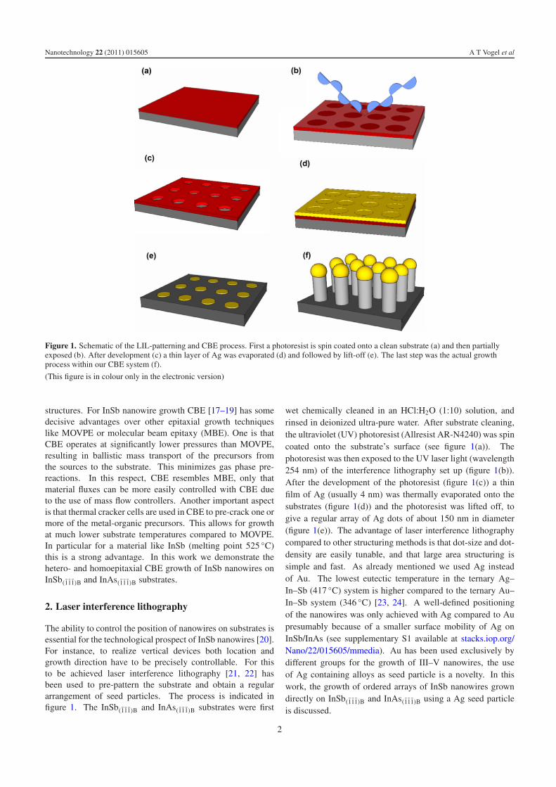
Figure 1. Schematic of the LIL-patterning and CBE process. First a photoresist is spin coated onto a clean substrate (a) and then partiallyexposed (b). After development (c) a thin layer of Ag was evaporated (d) and followed by lift-off (e). The last step was the actual growthprocess within our CBE system (f).
(This figure is in colour only in the electronic version)
structures. For InSb nanowire growth CBE [17–19] has somedecisive advantages over other epitaxial growth techniqueslike MOVPE or molecular beam epitaxy (MBE). One is thatCBE operates at significantly lower pressures than MOVPE,resulting in ballistic mass transport of the precursors fromthe sources to the substrate. This minimizes gas phase pre-reactions. In this respect, CBE resembles MBE, only thatmaterial fluxes can be more easily controlled with CBE dueto the use of mass flow controllers. Another important aspectis that thermal cracker cells are used in CBE to pre-crack one ormore of the metal-organic precursors. This allows for growthat much lower substrate temperatures compared to MOVPE.In particular for a material like InSb (melting point 525 ◦C)this is a strong advantage. In this work we demonstrate thehetero- and homoepitaxial CBE growth of InSb nanowires onInSb(111)B and InAs(111)B substrates.
2. Laser interference lithography
The ability to control the position of nanowires on substrates isessential for the technological prospect of InSb nanowires [20].For instance, to realize vertical devices both location andgrowth direction have to be precisely controllable. For thisto be achieved laser interference lithography [21, 22] hasbeen used to pre-pattern the substrate and obtain a regulararrangement of seed particles. The process is indicated infigure 1. The InSb(111)B and InAs(111)B substrates were first
wet chemically cleaned in an HCl:H2O (1:10) solution, andrinsed in deionized ultra-pure water. After substrate cleaning,the ultraviolet (UV) photoresist (Allresist AR-N4240) was spincoated onto the substrate’s surface (see figure 1(a)). Thephotoresist was then exposed to the UV laser light (wavelength254 nm) of the interference lithography set up (figure 1(b)).After the development of the photoresist (figure 1(c)) a thinfilm of Ag (usually 4 nm) was thermally evaporated onto thesubstrates (figure 1(d)) and the photoresist was lifted off, togive a regular array of Ag dots of about 150 nm in diameter(figure 1(e)). The advantage of laser interference lithographycompared to other structuring methods is that dot-size and dot-density are easily tunable, and that large area structuring issimple and fast. As already mentioned we used Ag insteadof Au. The lowest eutectic temperature in the ternary Ag–In–Sb (417 ◦C) system is higher compared to the ternary Au–In–Sb system (346 ◦C) [23, 24]. A well-defined positioningof the nanowires was only achieved with Ag compared to Aupresumably because of a smaller surface mobility of Ag onInSb/InAs (see supplementary S1 available at stacks.iop.org/Nano/22/015605/mmedia). Au has been used exclusively bydifferent groups for the growth of III–V nanowires, the useof Ag containing alloys as seed particle is a novelty. In thiswork, the growth of ordered arrays of InSb nanowires growndirectly on InSb(111)B and InAs(111)B using a Ag seed particleis discussed.
The system being used for the InSb nanowire growth wasa non-commercial cold wall chemical beam epitaxy (CBE)system. Trimethylindium (TMIn) and Triethylantimony(TESb) were the precursor materials used in this study. Theprecursors were held at constant temperature of 42.5 ◦C toensure a constant vapor pressure of the sources during thegrowth process. Commercially available mass flow controllers(MKS 1150C) were used to introduce a well-defined precursorflux into the chamber. The chamber was evacuated to a basepressure of 5 × 10⁻⁹ mbar. During growth the chamberpressure generally was in the range of 10−5–10−4 mbardepending on the actual precursor fluxes. In order to ensuregood homogeneity on the substrate the precursors were led intothe chamber via specially designed gas injectors. TESb has ahigh dissociation energy. To pre-crack TESb, the precursor wasinjected through a thermal cracker cell held at temperaturesaround 625 ◦C. TMIn, in contrast, is introduced into thegrowth chamber through an injector held at about 70 ◦C.The decomposition of TMIn starts at temperatures around300 ◦C [25], and it is assumed to decompose only at the surfaceof the heated substrate. Since the decomposition of TMIn is astrongly temperature dependent process, CBE growth heavilydepends on the substrate temperature. Furthermore, sinceCBE is a kinetically controlled growth process, the structureand morphology of the nanowires also critically depends onthe absolute In and Sb precursor fluxes as well as the V–III-ratio. In this study growth takes place at substrate temperaturesbetween 340 and 400 ◦C. No annealing was performed beforegrowth. All samples were grown with a TMIn flux of0.175 sccm and a V–III-ratio of 2. Precursors were turned offafter 25 min of growth and the samples were cooled down invacuum.
4. Results and discussions
Figures 2(a) and (b) show tilted scanning electron microscopy(SEM) images of InSb nanowires grown on InSb(111)B andon InAs(111)B substrates. The samples shown were grownat substrate temperatures of 380 ◦C and 360 ◦C respectively.It should be noted that on the InSb(111)B substrate a thickparasitic InSb layer in the space between nanowires formed.In contrast, on the InAs(111)B substrate little parasitic growthoccurred at the foot of the nanowires. Correlating theinitial Ag particle volume to the volume of the seed particleobserved on top of the nanowires after growth suggestedthat a metallic alloy with ∼20 at.% Ag promoted InSbnanowire growth. This was confirmed by post-growthenergy dispersive x-ray (EDX) experiments which revealedan Ag content of about 14 at.% inside the droplets fornanowires grown at 380 ◦C. Post-growth x-ray diffraction(XRD) investigations after different cooling procedures (seesupplementary S2 available at stacks.iop.org/Nano/22/015605/mmedia) also confirmed that nanowire growth was promotedby an Ag–In alloy. All experiments consistently indicate thatan In-rich alloy promoted InSb nanowire growth. According tothe Ag–In phase diagram, at 380 ◦C about 27 at.% of Ag can be
Figure 2. SEM micrographs of ordered InSb nanowire arrays grownon InSb(111)B (a) and on InAs(111)B (b). The substrate temperature wasset to 380 ◦C and 360 ◦C, respectively, during growth. On InSb(111)B aclosed layer of InSb surrounding the nanowires is clearly visible. OnInAs(111)B on the other hand, no closed film formed. Both insets showSEM top view images of the corresponding sample.
dissolved in liquid In–Ag alloys (possible In supersaturation isnot considered). We therefore conclude that the seed particle ismore likely to be liquid than solid during growth.
Most of the nanowires grew perpendicularly to thesubstrate surface and showed only little tapering (ratio of topdiameter to base diameter = 0.8) at 360 ◦C. Tapering is mostlikely caused by progressive reduction of the In content withinthe seed particle at low temperatures together with lateralovergrowth on the side facets at higher temperatures. Thismight explain the more severe tapering at higher temperaturessince parasitic InSb growth is also more pronounced (ratio oftop diameter to base diameter = 0.6 at 380 ◦C). It should benoted that the wire distance is not the same for the samplesshown in figure 2 and this difference in wire density might alsohave an influence on the nanowire morphology [26].
At 360 ◦C (on InAs substrate) 87% of the Ag islandsnucleated at least one InSb nanowire compared to the numberof lithographically pre-defined positions. While heating thesubstrate, the Ag islands could have also split into two alloydroplets which each catalyzed a nanowire. At 380 ◦C (on InSbsubstrate) however, only 43% of the Ag islands nucleated a
Figure 3. (a) The growth rate over substrate temperature for InSbnanowires and the grown parasitic thin film on a InSb(111)B substrate.(b) The growth rate of nanowires and thin film on InAs(111)B. Theerror bars account for the standard deviation. The dotted lines areinserted to guide the reader’s eye.
nanowire. This is probably caused by a higher mobility ofseed particles at higher substrate temperatures and hence morepronounced Ostwald ripening.
In order to maximize the nanowire-versus-thin-filmgrowth rate ratio, a series of growth experiments at differenttemperatures has been conducted. These results are shown infigure 3, where the growth rate of InSb nanowires (NW) as wellas the growth rate of the additional thin film (TF) is given as afunction of the substrate temperature for the two different typesof substrates: InSb(111)B and InAs(111)B. The growth rate wasdetermined by measuring wire length and thin film thicknessusing SEM and TEM images. For VLS grown nanowires thenanowire length also depends on the nanowire diameter [19].To circumvent this influence, only nanowires with diametersof 95–115 nm were considered for this evaluation. Eachdata point of the nanowire growth rate represents the meanof at least 50 nanowires, for which the length was measured.The error bars correspond to the standard deviation. Onecan see in figure 3(a) that the nanowire growth rate reachesa maximum at a substrate temperature of about 380 ◦C on
both InSb(111)B and InAs(111)B substrates, in correspondenceto what has been observed in MBE [27]. The increase of thenanowire growth rates from 340 to 380 ◦C can be attributedto the increased TMIn decomposition and the correspondinglarger In supply. Reducing the temperature also reduces thinfilm growth, and at 340 ◦C only insignificant film growth can beobserved. Considering figure 3(a) it can be anticipated that fortemperatures higher than about 400 ◦C the growth rate for thethin film even exceeds the nanowire growth rate. Furthermore,results show that in order to maximize the nanowire-versus-thin-film growth rate ratio, a quite low substrate temperature ofaround 340 ◦C should be applied.
Considering InSb growth on InAs(111)B, figure 3(b), themaximum nanowire growth rate is also reached at about380 ◦C. It should be noted that the overall growth rates aresomewhat smaller than the growth rates observed for growthon InSb(111)B. This can potentially be attributed to reduceddiffusion or increased desorption of the In precursor specieson InAs(111)B compared to InSb(111)B and the correspondinglyreduced In supply for InSb growth. Insufficient dataconcerning adatom diffusion under CBE conditions exist toverify this. Another possible cause could be that thin filmgrowth is influenced by the lattice mismatch of about 7%which could potentially decrease growth rates. It is worthemphasizing that for substrate temperatures of 360 ◦C andbelow, absolutely no thin film growth takes place and hencefree-standing InSb nanowires on InAs(111)B substrates can befabricated.
Figure 4(a) shows a cross-section bright-field TEM imageof a InSb nanowire grown on InSb(111)B at a substratetemperature of 380 ◦C. As expected from the previously showngrowth rate investigations, a defect rich InSb layer embeddingthe nanowires is clearly visible. Figure 4(b) shows a cross-section bright-field TEM image of an InSb nanowire grownon InAs(111)B. The substrate temperature was set to 340 ◦C.As growth rate evaluations suggested, no parasitic thin filmgrew. It should be mentioned that samples used for TEMinvestigations were grown from non-structured samples ontowhich a 2 nm thick Ag film had been deposited.
Figure 5(a) shows a high resolution TEM image of anInSb nanowire grown at 340 ◦C. A high number of stackingfaults and twin defects can be observed. Figure 5(b) shows thecorresponding fast Fourier transform (FFT). The nanowire isof cubic zinc blende structure and the characteristic streakingcaused by the large number of stacking faults is clearly visible.Figure 5(d) shows a high resolution TEM image of an InSbnanowire grown at 380 ◦C. The number of stacking faultswithin the nanowire is significantly reduced. Instead, twinningoccurs, as confirmed by the corresponding FFT shown infigure 5(c). The twin segments were each about 20 nm inheight. Previous reports on InSb nanowire growth [11, 15, 16]showed nearly perfect InSb nanowires without any planardefects. Caroff et al [28] showed that nanowires grown atlow substrate temperatures exhibit a larger number of planardefects than wires grown at higher temperatures. So, weattribute the formation of planar defects to the overall lowergrowth temperatures and to a seed particle, that (mostlyconsisting of In) is not lattice matched to InSb.
4
Nanotechnology 22 (2011) 015605 A T Vogel et al
Figure 4. (a) Cross-section TEM micrograph of InSb nanowiresgrown on InSb(111)B substrate at a growth temperature of 380 ◦C. Theadditional defect rich InSb thin film embedding the InSb nanowiresis clearly visible. (b) TEM micrograph of InSb nanowires grown at340 ◦C on InAs(111)B. Under these conditions no additional InSb thinfilm formed.
Figure 6 shows three Raman spectra that were acquiredwith the 488 nm emission line of an Ar+-ion laser (spotdiameter about ≈1 µm, energy density ≈8×10⁴ W cm−2). Theupper gray curve corresponds to the Raman spectrum of a pieceof bulk InSb. The two pronounced peaks at ≈180 cm−1 and≈190 cm−1 correspond to the twofold degenerate transverseoptical (2 × TO) phonon modes and to the one longitudinaloptical (LO) mode, respectively. The lower gray curve displaysthe Raman spectrum of bulk InAs. Analogously to bulk InSb,the lower wavenumber peak (≈220 cm−1) belongs to the twodegenerate TO modes and the peak at ≈240 cm−1 to the LOmode. Analogously to all other polar semiconductors withzinc blende structure (e.g. GaAs, GaP, InP) the frequency ofthe LO phonon is higher. This is because electric fields buildup in the crystal during an LO lattice oscillation increasing theeffective force constant, which then results in a higher phononfrequency.
The black graph represents the Raman spectrum ofa sample where InSb nanowires were grown on an InAssubstrate. In this case, the Raman peaks corresponding to
Figure 5. (a) An HRTEM image of an InSb nanowire grown at340 ◦C. (b) The corresponding FFT. A large number of planar defectsis clearly visible and leads to extensive streaking in the FFT. (d) AnHRTEM image of an InSb nanowire grown at 380 ◦C. The number ofplanar defects is heavily reduced and only well-defined twinningoccurred (see FFT in (c)). Black arrows mark twin boundaries. Thewhite arrows mark sections of the nanowire with high stacking faultdensities.
the optical phonon modes of InSb and InAs are visible. Theslight shift of the InSb Raman bands to higher wavenumberscompared to bulk InSb (see inset figure 6) might be caused bythe stress at the nanowire/substrate interface as the InAs peaksare also slightly shifted.
The influences of the phonon confinement effects insemiconductor nanostructures always lead to a shift of phononfrequencies to lower wavenumbers and therefore also to adecrease of the Raman peak positions (due to the relaxationof the zero-wavevector selection rule at the Brillouin zonecenter and the always negative slope of the phonon dispersioncurves close to the zone center). The absence of this shiftindicates that the diameters of the grown InSb nanowires (100–250 nm) are too large for observable phonon confinement
5
Nanotechnology 22 (2011) 015605 A T Vogel et al
Figure 6. Raman spectra of a bulk InSb sample (upper gray curve),of a bulk InAs sample (lower gray curve), and of a sample whereInSb nanowires were grown on a InAs substrate (black; see text for adetailed description). The inset shows a magnification of the areaindicated.
effects. Generally, phonon confinement effects in othersemiconductor nanostructures (Si nanowires, etc) usuallyrequire characteristic sizes of less than 30 nm [29, 30] whichagrees with our findings. A detailed Raman analysis of InSbnanowires that addresses phonon confinement effects and theinfluence of crystal defects on the lattice oscillations is inprogress.
5. Conclusions
In summary, we have demonstrated the homo- and heteroepi-taxial growth of InSb nanowires directly on InSb(111)B andInAs(111)B substrates. Instead of Au we used lithographicallystructured Ag seed particles for nanowire growth. Weinvestigated the growth rate of both InSb nanowires andparasitic InSb thin films on InAs and InSb substrates. Wewere able to show that the growth rate of the parasitic InSbthin film is strongly reduced on InAs(111)B substrates. Byapplying low growth temperatures, this allowed us to growfree-standing InSb nanowires without any parasitic InSb thinfilm. TEM investigations, however, showed that nanowiregrowth at temperatures as low as 340 ◦C results in a higherdensity of stacking faults within the wires.
Acknowledgments
We want to thank Dr Stephan Senz for helpful discussions. Wealso want to thank Mrs Hopfe for TEM sample preparation.
The financial support by the NANOSTRESS project isgratefully acknowledged. Above all we would like to expressour deep gratitude to Professor U Gosele for all the relentlesssupport and encouragement.
References
[1] Riikonen J et al 2005 J. Mater. Sci., Mater. Electron. 16 449–53[2] Heyns M and Tsai W 2009 MRS Bull. 34 485–92[3] Ashley T et al 2004 7th Int. Conf. on Solid-State and Integrated
Circuits Technology Proc. 3 2253–6[4] Nilsson H A, Philippe C, Thelander C, Lind E, Karlstrom O and
Wernersson L-E 2010 Appl. Phys. Lett. 96 153505[5] Paul R K, Penchev M, Zhong J B, Ozkan M, Ghazinejad M,
Jing X Y, Yengel E and Ozkan C S 2010 Mater. Chem. Phys.121 397–401
[6] Zhang X W, Li S S and Xia J B 2006 Appl. Phys. Lett.89 172113
[7] Mingo N 2004 Appl. Phys. Lett 84 2652–4[8] Nilsson A H, Caroff P, Thelander C, Larsson M, Wagner J B,
Wernersson L, Samuelson L and Xu H Q 2009 Nano Lett.9 3151–6
[9] Service R F 2009 Science 323 1000–2[10] Larsson M W, Wagner J B, Wallin M, Hakansson P,
Froberg L E, Samuelson L and Wallenberg L R 2007Nanotechnology 18 15504–11
[11] Caroff P, Messing M E, Borg B M, Dick K A, Deppert K andWernersson L-E 2009 Nanotechnology 20 495606
[12] Park H D, Prokes S M, Twigg M E, Ding Y and Wang Z L 2007J. Cryst. Growth 304 399–401
[13] Vaddiraju S, Sunkara M K, Chin A H, Ning C Z, Dholakia G Rand Meyyappan M 2007 J. Phys. Chem. C 111 7339–47
[14] Yang Y, Li L, Huang X, Li G and Zhang L 2007 J. Mater. Sci.42 2753–7
[15] Caroff P, Wagner J B, Dick K A, Nilsson H A, Jeppsson M,Deppert K, Samuelson L, Wallenberg L R andWernersson L-E 2008 Small 4 878–82
[16] Ercolani D, Rossi F, Li A, Roddaro S, Grillo V, Salviati G,Beltram F and Sorba L 2009 Nanotechnology 20 505605
[17] Persson A I, Ohlsson B J, Jeppesen S and Samuelson L 2004J. Cryst. Growth 272 174–6
[18] Jensen L E, Bjork M T, Jeppesen S, Persson A I, Ohlsson BJ and Samuelson L 2004 Nano Lett. 4 1961–4
[19] Persson A I, Froeberg L E, Jeppesen S, Bjoerk M T andSamuelson L 2007 J. Appl. Phys. 101 034313
[20] Thelander C et al 2006 Mater. Today 9 28–35[21] de Boor J, Geyer N, Gosele U and Schmidt V 2009 Opt. Lett.
34 1783–5[22] de Boor J, Geyer N, Wittemann J V, Gosele U and
Schmidt V 2010 Nanotechnology 21 095302[23] Liu H S, Liu C L, Wang C, Jin Z P and Ishida K 2003
J. Electron. Mater. 32 81–7[24] Liu X J, Yamaki T, Ohnuma I, Kainuma R and Ishida K 2004
Mater. Trans. 45 637–45[25] Fan G H, Hoare R D, Pemble M E, Povey I M, Taylor G and
Williams J O 1992 J. Cryst. Growth 124 49–55[26] Messing M E, Hillerich K, Bolinsson J, Storm K, Johansson J,
Dick K A and Deppert K 2010 Nano Res. 3 506–19[27] Debnath M C, Zhang T, Roberts C, Cohen L F and
Stradling R A 2004 J. Cryst. Growth 267 17–21[28] Caroff P, Dick K A, Johansson J, Messing M E, Deppert K and
Samuelson L 2009 Nat. Nanotechnol. 4 50–5[29] Richter H, Wang Z P and Ley L 1981 Solid State Commun.
39 625–9[30] Campbell I H and Fauchet P M 1986 Solid State Commun.