40
Spark-102 Altera Cyclone V SOC System on Module Integration guide Revision – 1.2
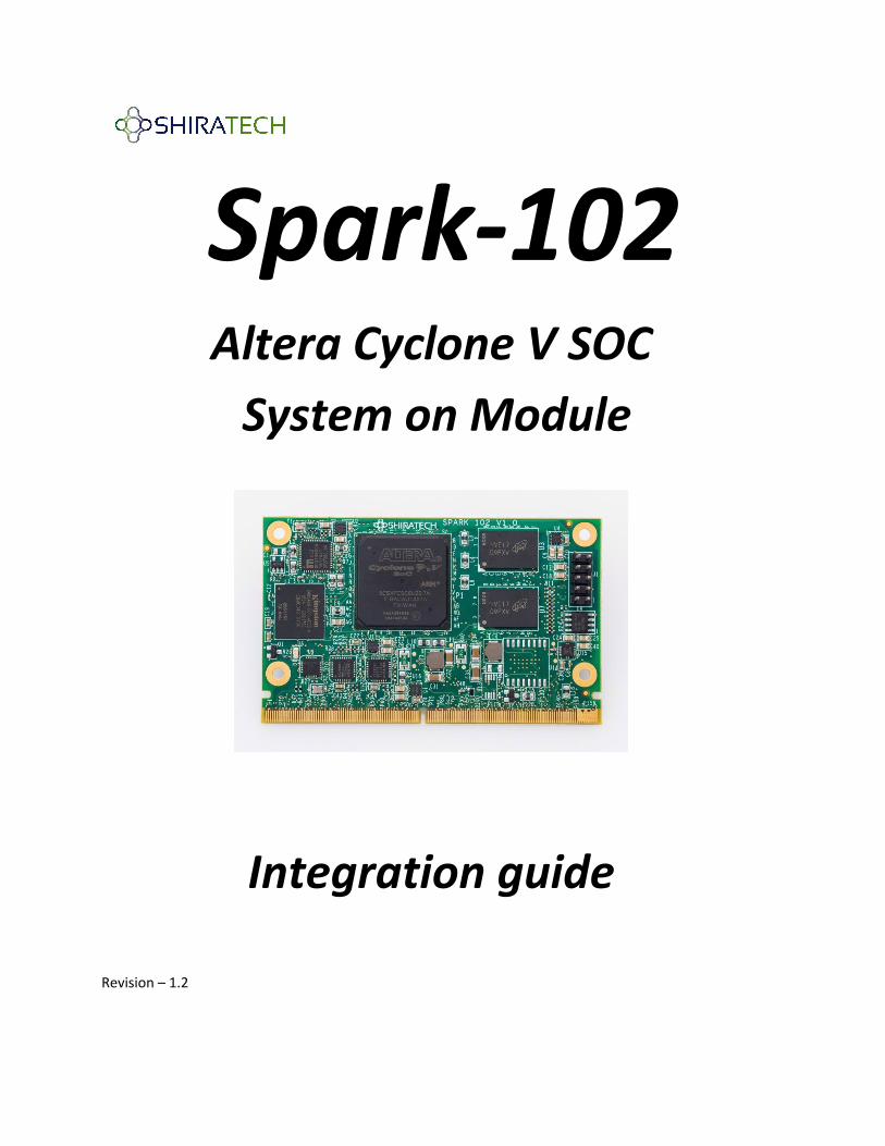
Spark-102 Altera Cyclone V SOC
System on Module
Integration guide
Revision – 1.2

2 | Spark-102 HW user manual V1.3
Contents 1 Scope ............................................................................................................................................... 4
1.1 SoM introduction ........................................................................................................................ 4
2 Block diagram .................................................................................................................................. 5
3 SOM integration – system aspects ................................................................................................... 5
3.1 Power considerations ................................................................................................................. 5
3.1.1 VCCBAT – FPGA Encryption Key power ............................................................................... 5
3.1.2 Spark Power scheme .......................................................................................................... 6
3.2 Reset sources .............................................................................................................................. 7
3.3 Clocks scheme ............................................................................................................................ 8
3.4 Temperature sensor.................................................................................................................... 8
3.5 JTAG ........................................................................................................................................... 8
4 HPS system and Interfaces ............................................................................................................... 9
4.1 HPS Memories scheme ............................................................................................................... 9
4.1.1 QSPI NOR memory ............................................................................................................ 10
4.1.2 EEPROM ........................................................................................................................... 10
4.1.3 eMMC (iNAND) ................................................................................................................. 10
4.1.4 SD/eMMC interface .......................................................................................................... 10
4.1.5 DDR memory .................................................................................................................... 10
4.2 Boot options ............................................................................................................................. 11
4.3 FPGA Firmware configuration options ....................................................................................... 12
4.4 Interrupt & I/O Table ................................................................................................................ 13
4.5 HPS interfaces ........................................................................................................................... 14
4.5.1 HPS USB Interfaces ........................................................................................................... 14
4.5.2 Ethernet port .................................................................................................................... 14
4.5.3 UART ................................................................................................................................ 15
4.5.4 CAN .................................................................................................................................. 15
4.5.5 I2C .................................................................................................................................... 16
4.5.6 SPI .................................................................................................................................... 16
5 SOC FPGA part ............................................................................................................................... 17
5.1 FPGA Banks ............................................................................................................................... 17
5.2 FPGA IOs ................................................................................................................................... 18

3 | Spark-102 HW user manual V1.3
5.3 FPGA IOs variation according to FPGA size ................................................................................ 18
5.4 Transceivers .............................................................................................................................. 19
5.5 FPGA configuration ................................................................................................................... 19
5.5.1 Configuration via byte blaster ........................................................................................... 19
5.5.2 Configuration via Software ............................................................................................... 19
5.6 Industrial Ethernet module ....................................................................................................... 20
5.7 CSEL Configuration .................................................................................................................... 22
6 SMARC interface Pin assignment ................................................................................................... 22
7 Mechanical considerations ............................................................................................................ 27
7.1 SMARC connector ..................................................................................................................... 28
Appendix 1 - Hardware devices used on the SOM .................................................................................. 30
Appendix 2 – Hardware configuration summary .................................................................................... 31
Appendix 3 – Qsys parameters for the Spark ......................................................................................... 32
Document Revision History
Revision Date Description
1.0 2.2.2016 Initial version
1.1 22.8.2016 Add internal Ethernet PHY connectivity to the FPGA, add phy reset description.
1.2 28.9.2016 Add support for Spark-102v2
4 | Spark-102 HW user manual V1.3
1 Scope The purpose of this document is to provide a guide for integrating the Spark-102 into the target
hardware in an easy and fast way to shorten and simplify the development process.
The guide is divided into two parts, the first guide you through the integration process, giving design
samples based on the CB-52 development board (schematics can be provided by Shiratech via
[email protected] ), the second part provides a more detailed description of the Spark-102
system.
In order to simplify the integration process we recommend the following process:
1. Read through the integration guide about the required interfaces.
2. Use Shiratech’s Pin configuration tool to define the solution
3. Use the CB-52 as a reference design and schematics to shorten the development process.
For more details if needed, review the Cyclone V user manual.
1.1 SoM introduction The Spark-102 is an industrial embedded System-On-Module (SoM) based on Altera new Cyclone V SoC.
The Spark-102 offers a unique combination of a high performance ARM core containing one or two
Cortex-A9 cores combined with a large FPGA offering up to 110KLE.
The Spark-102 enables the end user to create a tailored solution made of the ARM processor variety of
interfaces combined with additional "Soft Core" interfaces based on the FPGA. The unique
interconnection between the FPGA and ARM core enables the ARM processor to access the FPGA based
interfaces as regular slave interfaces.
For industrial automation product development the Spark offers built-in Industrial Ethernet core
including dedicated Ethernet ports, built-in FPGA IP and full Linux support reduce R&D efforts, risk and
time.
The Spark-102 supports the SMARC standard developed by SGET (www.sget.org) utilizing a 314 interface
connector providing a rich and flexible interface towards the carrier board.
The module has several configuration options for supporting the various Altera SOC sizes and variations
along with different memory sizes to support the various project's needs.
5 | Spark-102 HW user manual V1.3
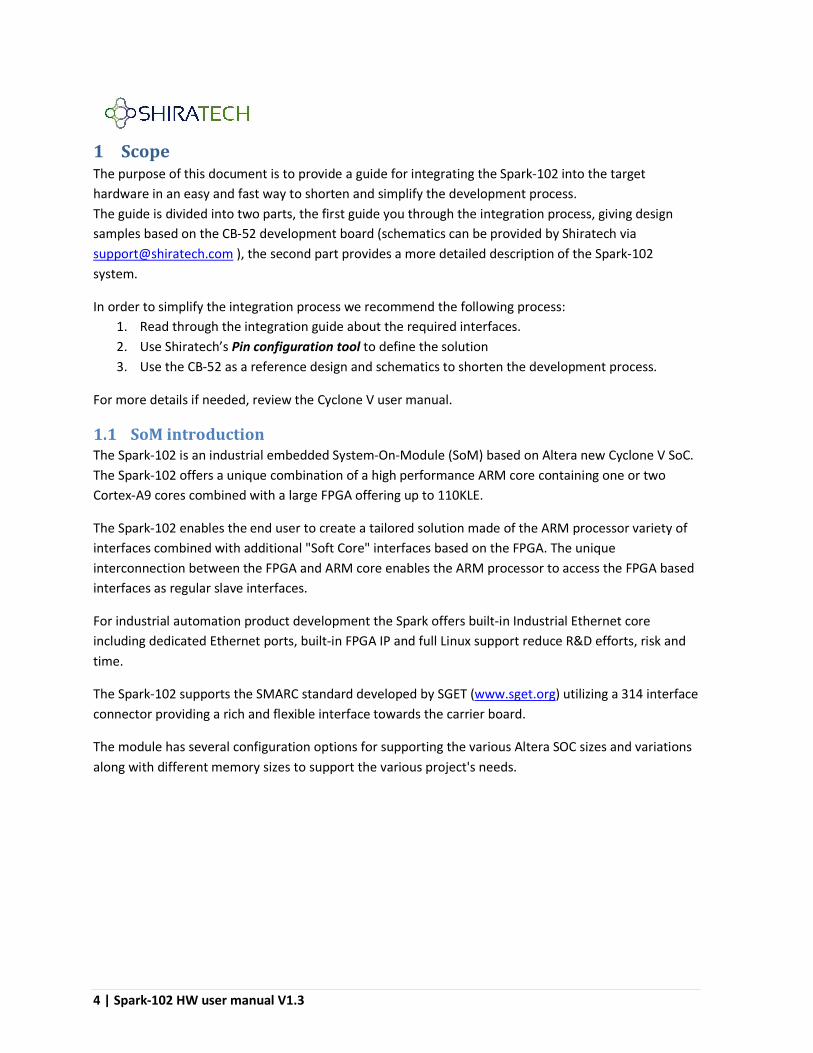
2 Block diagram The following diagram provides an overview of the SOM. The following paragraphs will provide detailed
description of the various parts of the SOM and how to use them in order to build a product based on it.
Figure 1 – SOM main building blocks
3 SOM integration – system aspects
3.1 Power considerations The Spark-102 uses a single 5V power input from which all the other required voltages are taken. The
Inlet power should be
Rise time: <= 3ms
Input voltage range: 5V +/- 5%
3.1.1 VCCBAT – FPGA Encryption Key power
The Altera SOC has an option to maintain an encryption key for FPGA configuration even if the system
power is down. For that pin S147 of the SMARC interface should be connected to a power source
(between 1.2V - 3V). If the option is not used connect pin S147 to 2.5V. The interface is connected to
VCCBAT (D7) pin of the SOC.
ECAT BLOCK
ARM 9CORE
eMMC4-64 GB
MM
C D
[0..
7]
SerialNOR
QS
PI
(CS
0)
PWRMng.
PIN MUX
GEPHY
RGMII
SMARK
TX/RX
USB OTG
SPI 0,1 (4 x CS)
I2C 0,1
USART 0 (RX/TX)
CAN 0,1
PWR_En, WKUP, Idle, Sleep
FPGA
DDR3
D[0
-31
]
SDMUX
FEPHY
FEPHY
BANK3A/B
CPLD(AUT)
EEPROM
BANK8A/5B
BANK4A
BANK5A
USBPHY
QSPI (CS1)
UMTI
MMCD[0..3]
TRANS
ClockDriver
uDS
MII
MII
I2C
I/O
SMARK
100BT
100BT
DIFF. CLK
6 x SER/DES
64 I/O, 4 CLK
LVDS DISPLAY, 16 I/O
CSI 2 LANE, I/O
ClockDriver
6 | Spark-102 HW user manual V1.3
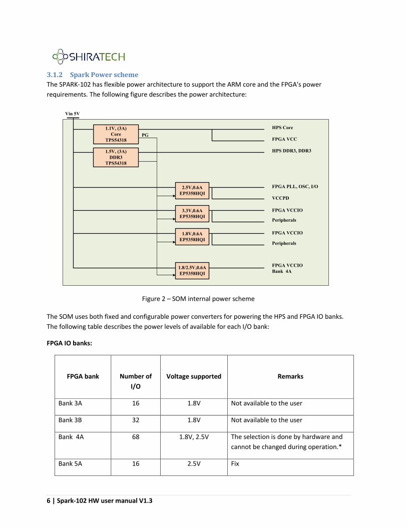
3.1.2 Spark Power scheme
The SPARK-102 has flexible power architecture to support the ARM core and the FPGA's power
requirements. The following figure describes the power architecture:
Figure 2 – SOM internal power scheme
The SOM uses both fixed and configurable power converters for powering the HPS and FPGA IO banks.
The following table describes the power levels of available for each I/O bank:
FPGA IO banks:
FPGA bank
Number of
I/O
Voltage supported
Remarks
Bank 3A 16 1.8V Not available to the user
Bank 3B 32 1.8V Not available to the user
Bank 4A 68 1.8V, 2.5V The selection is done by hardware and
cannot be changed during operation.*
Bank 5A 16 2.5V Fix
1.1V, (3A)Core
TPS54318
1.5V, (3A)DDR3
TPS54318
2.5V,0.6AEP5358HQI
3.3V,0.6AEP5358HQI
1.8V,0.6AEP5358HQI
Vin 5V
HPS Core
FPGA VCC
HPS DDR3, DDR3
FPGA PLL, OSC, I/O
VCCPD
FPGA VCCIO
Peripherals
Peripherals
FPGA VCCIO
FPGA VCCIOBank 4A
PG
1.8/2.5V,0.6AEP5358HQI
7 | Spark-102 HW user manual V1.3
Bank 5B 7 2.5V Fix
Bank 8A 6 2.5V Fix
*Notes:
Bank 4A power level is controlled via a dedicated pin on the SMARC interface, Bank 4A VCC IO
located on P106.
- When connected to GND then VCCIO is set 1.8V, when connected to VCC then VCCIO is set to 2.5V.
- The pin setting cannot be based on I/O controlled by software! the pin state should be stable
at power up and cannot be changed after power up.
HPS IO banks:
HPS bank Voltage supported Remarks
Bank 6 1.5V Internal bank for DDR
7A 1.8V Various interfaces,
7B, 7C 3.3V Various interfaces, like SD and USB
3.2 Reset sources The SPARK-102 supports three reset sources:
Cold reset (Power On Reset - RESET_IN# – P127 on the SMARC interface) o Used to ensure the HPS is placed in a default state sufficient for software to boot o Triggered by a power-on reset and other sources e.g. push buttons on carrier board o Resets all HPS logic that can be reset o Affects all reset domains
Warm reset (FORCE_RECOV# - S155 on the SMARC interface) o Occurs after HPS has already been through a cold reset o Used to recover system from a non-responsive condition o Resets a subset of the HPS state reset by a cold reset o Only affects the system reset domain, which allows debugging (including trace) to operate
through the warm reset
Debug Reset o Occurs after HPS has already been through a cold reset o Used to recover debug logic from a non-responsive condition o Only affects the debug reset domain
The cold and warm resets are controlled by voltage supervisors which guarantee the reset duration.
Both signals are available on the SMARC connector. The FPGA can be reset by the SOC ARM core or by
an IO pin on the FPGA fabric.

8 | Spark-102 HW user manual V1.3
Note:
When using the 128 MB QSPI Flash memory as a boot source the warm reset does not work
automatically due to configuration issues of the QSPI memory. For more details:
http://www.rocketboards.org/foswiki/Documentation/SocBoardQspiBoot
For 32MB QSPI Flash memory configuration the problem is resolved.
3.3 Clocks scheme The SPARK-102 contains a single clock buffer which distributes a 25 MHz clock to the HPS core, the FPGA
clock input 1 and 2 and to the Industrial Ethernet PHY devices. The following figure describes the clock
architecture.
Figure 3 – SPARK-102 Clock Architecture
3.4 Temperature sensor The Spark has a build in temperature sensor based on TI Digital Temperature Sensor TMP 108. The
device is controlled via I2C1 bus.
3.5 JTAG A 10 pins JTAG connector for byte blaster connectivity is available on the SOM, the connector will be
available for development when the SOM is provided with the evaluation board or as an ordering
option.
Fan OutBuffer
25 MHz
HPS CLK1
HPS CLK2
FPGA CLK1
FPGA
SMARC CONNECTOR
HPS
FPGA CLK2CLKI0_p
CLKI1_p
Transceiver CLKI
Transceiver CLKI
Single ended 25 MHz
100, 125, Other Differential
Single End, Differential
Local OSC 25 MHZ
CL
KI2
_n/p
CLK
CLK
CL
KI3
_n/p
CL
KI4
_n
/p
CL
KI5
_n
/p
Basic Clock
CL
KI6
_n
/p
CL
KI7
_n
/p
Fast Ethernet(ECAT)
Fast Ethernet(ECAT)

9 | Spark-102 HW user manual V1.3
4 HPS system and InterfacesThe Spark-102 can be ordered with
SOM offers a variety of interfaces from the HPS
more. The following paragraphs describe
on how to connect them to the carrier board.
4.1 HPS Memories schemeThe SPARK-102 includes several options for non
including:
- A QSPI NOR memory (32MB or 128MB), can be used for a small footprint Linux
- Internal eMMC device of 4GB up to 8GB
software and storage.
- A small I2C memory 128x8 EEPROM, used for card details and can be used for system
parameters.
Figure 4
V1.3
Interfaces can be ordered with one or two ARM cores running at 800Mhz or 925Mhz (grade 6). The
a variety of interfaces from the HPS (ARM core) such as USB, Ethernet, I2C, SPI, UART and
paragraphs describe the various interfaces available along with recomme
on how to connect them to the carrier board.
scheme 102 includes several options for non-volatile memories for booting and data storage,
A QSPI NOR memory (32MB or 128MB), can be used for a small footprint Linux
Internal eMMC device of 4GB up to 8GB(for larger size please contact Shiratech)
A small I2C memory 128x8 EEPROM, used for card details and can be used for system
Figure 4 – SPARK-102 Non-Volatile Memory
one or two ARM cores running at 800Mhz or 925Mhz (grade 6). The
(ARM core) such as USB, Ethernet, I2C, SPI, UART and
the various interfaces available along with recommendations
volatile memories for booting and data storage,
A QSPI NOR memory (32MB or 128MB), can be used for a small footprint Linux version or RTOS.
(for larger size please contact Shiratech), used for both
A small I2C memory 128x8 EEPROM, used for card details and can be used for system
10 | Spark-102 HW user manual V1.3
4.1.1 QSPI NOR memory
The Spark supports a QSPI NOR memory. The memory is connected to the QSPI interface of the HPS
offering:
4 bits Data bus.
Up to 108MHz clock.
32Mbytes - optional.
4.1.2 EEPROM
The Spark-102 is supports an internal I2C memory device Atmel AT24C01Ce, located on I2C0 bus of the
HPS offering:
1Kbit I2C memory.
Can be used as secure boot.
Can be used as MAC address for the GE interface. Note: part of the memory is internally used for card parameters.
4.1.3 eMMC (iNAND)
The Spark supports a 4GByte eMMC device offering:
Up to 8 data bits.
Up to 50 MHz clock. An 8GByte option is available as an ordering option.
4.1.4 SD/eMMC interface
The SPARK-102 has a single SD/MMC bus connected to the HPS. The HPS is connected via an internal
multiplexer (TXS02612 - SDIO Port Expander by TI) to either an internal 4/8 bits wide eMMC or to an
external 4 bits SD interface.
The control of the mux is via an external pin P123 in the SMARC interface, ‘0’ – eMMC, ‘1’ - external SD,
or via software using GPIO 44 of the HPS.
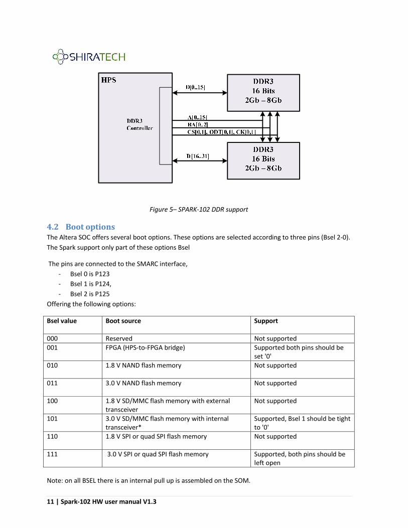
4.1.5 DDR memory
The SPARK-102 integrates 32 bit wide DDR3 running at 400 MHz. The basic configuration is two chips of
256MBx16 (1GB solution). There is also an ordering options for 128MBx16 (512MB solution) and
512MBx16 (2GB solution).
11 | Spark-102 HW user manual V1.3
Figure 5– SPARK-102 DDR support
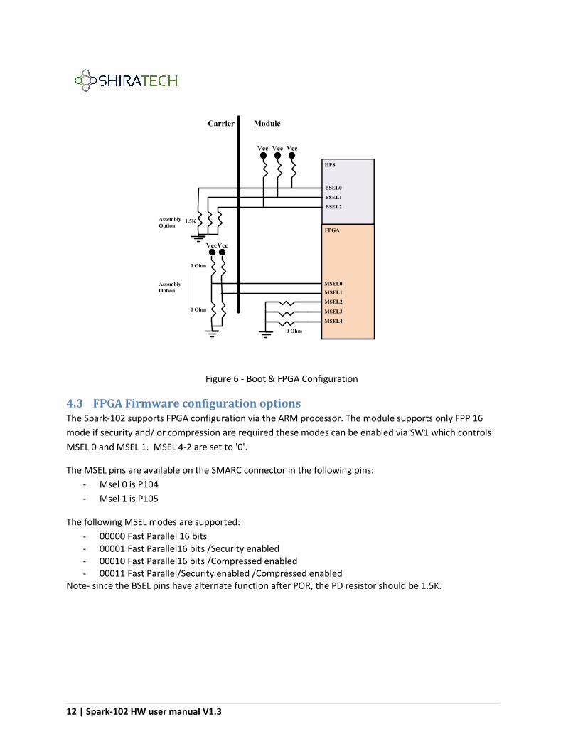
4.2 Boot options The Altera SOC offers several boot options. These options are selected according to three pins (Bsel 2-0).
The Spark support only part of these options Bsel
The pins are connected to the SMARC interface,
- Bsel 0 is P123
- Bsel 1 is P124,
- Bsel 2 is P125
Offering the following options:
Bsel value
Boot source Support
000 Reserved Not supported
001 FPGA (HPS-to-FPGA bridge) Supported both pins should be set '0'
010
1.8 V NAND flash memory Not supported
011
3.0 V NAND flash memory Not supported
100 1.8 V SD/MMC flash memory with external transceiver
Not supported
101 3.0 V SD/MMC flash memory with internal transceiver*
Supported, Bsel 1 should be tight to '0'
110 1.8 V SPI or quad SPI flash memory
Not supported
111 3.0 V SPI or quad SPI flash memory Supported, both pins should be left open
Note: on all BSEL there is an internal pull up is assembled on the SOM.
12 | Spark-102 HW user manual V1.3
Figure 6 - Boot & FPGA Configuration
4.3 FPGA Firmware configuration options The Spark-102 supports FPGA configuration via the ARM processor. The module supports only FPP 16
mode if security and/ or compression are required these modes can be enabled via SW1 which controls
MSEL 0 and MSEL 1. MSEL 4-2 are set to '0'.
The MSEL pins are available on the SMARC connector in the following pins:
- Msel 0 is P104
- Msel 1 is P105
The following MSEL modes are supported:
- 00000 Fast Parallel 16 bits - 00001 Fast Parallel16 bits /Security enabled - 00010 Fast Parallel16 bits /Compressed enabled - 00011 Fast Parallel/Security enabled /Compressed enabled
Note- since the BSEL pins have alternate function after POR, the PD resistor should be 1.5K.
HPS
FPGA
MSEL0
MSEL1
MSEL2
MSEL3
MSEL4
BSEL0
BSEL1
BSEL2
Vcc
ModuleCarrier
1.5K
Vcc Vcc
VccVcc
0 Ohm
0 Ohm
0 Ohm
AssemblyOption
AssemblyOption

13 | Spark-102 HW user manual V1.3
4.4 Interrupt & I/O Table The following table describes the role of the various HSP IO used on the Spark:
Signal I/O Description Remarks
SD_MMC_SEL GPIO44 Select between eMMC on SOM and
uSD on carrier
0 – eMMC
1 - uSD
SD_PWR_EN GPIO37 Enable power to the carrier uSD card Active High
GE Interrupt GPI2 Giga Ethernet Interrupt from PHY Active Low
TEMP_ALM GPI3 Temperature Sensor Alarm Active Low
FE Interrupt GPI1 Fast Ethernet Interrupt Active Low
RTC ALARM GPI0 Real Time Clock Alarm Active Low
14 | Spark-102 HW user manual V1.3
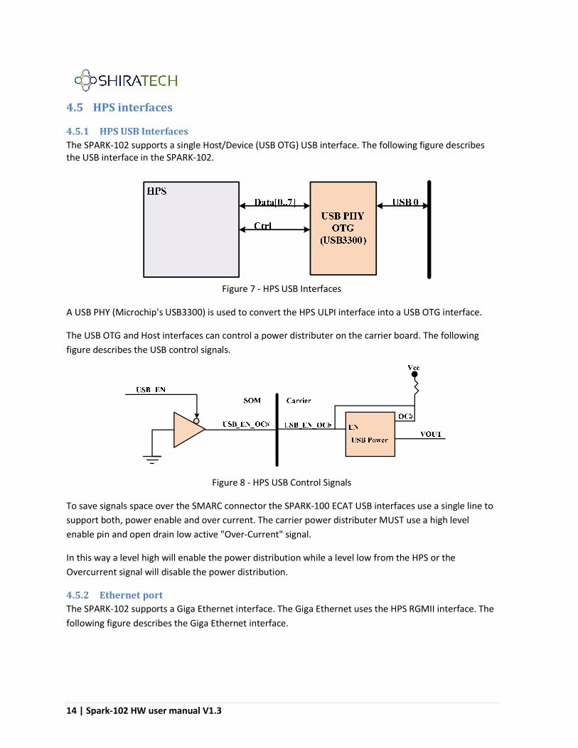
4.5 HPS interfaces
4.5.1 HPS USB Interfaces
The SPARK-102 supports a single Host/Device (USB OTG) USB interface. The following figure describes the USB interface in the SPARK-102.
Figure 7 - HPS USB Interfaces
A USB PHY (Microchip's USB3300) is used to convert the HPS ULPI interface into a USB OTG interface.
The USB OTG and Host interfaces can control a power distributer on the carrier board. The following
figure describes the USB control signals.
Figure 8 - HPS USB Control Signals
To save signals space over the SMARC connector the SPARK-100 ECAT USB interfaces use a single line to
support both, power enable and over current. The carrier power distributer MUST use a high level
enable pin and open drain low active "Over-Current" signal.
In this way a level high will enable the power distribution while a level low from the HPS or the
Overcurrent signal will disable the power distribution.
4.5.2 Ethernet port
The SPARK-102 supports a Giga Ethernet interface. The Giga Ethernet uses the HPS RGMII interface. The
following figure describes the Giga Ethernet interface.

15 | Spark-102 HW user manual V1.3
Figure 9 - Giga Ethernet Interfaces
The 1G Ethernet PHY is Micrel's KSZ9031. It uses an RGMII interface running at 125 MHz. The 125 MHz
clock is generated by the KSZ9031 Giga Ethernet PHY.
The 1G Ethernet PHY analog signals (TX+/-, RX+/-) are connected to the SMARC edge connector. Two led
signal from the GE PHY are also connected to the SMARC edge connector.
MDC/MDIO - The Ethernet MDC/MDIO signals are connected to the internal phy and are not available
on the SMARC connector.
4.5.3 UART
The SOC offer one or two UARTs. Each UART includes Rx, Tx , CTS and RTS. The HPS supports up to two
UART interfaces. UART 0 is usually used for Linux CLI interface. Some of the UART signals share the same
pins as the SPI interfaces which available on the SMARC connector.
UART0 TX/RX signals are available on the SMARC SER3 interface.
Programmable character properties, such as number of data bits per character, optional parity bits, and number of stop bits.
Programmable baud rate.
Automatic flow control mode per 16750 standards. The maximum UART baud rate is 6.25 mega symbols per second.
4.5.4 CAN
The HPS offers up to two CAN controllers based on the Bosch® D_CAN controller and offer the following
features:
Compliant with CAN protocol specification 2.0 part A & B.
Programmable communication rate up to 1 Mbps.
Holds up to 128 messages.
Supports 11-bit standard and 29-bit extended identifiers.
Programmable interrupt scheme.

16 | Spark-102 HW user manual V1.3
Direct access for host processor.
DMA controller may be used for large transfers.
4.5.5 I2C
The SPARK-102 supports two I2C master interfaces out of the HPS:
I2C0 is used as I2C_GP (SMARC standard).
I2C1 is used as I2C_PM (SMARC standard). On the Spark there are two I2C devices:
Serial EEPROM (AT24C01C by Atmel) which is located on I2C0 and is used for card parameters and user specific data and
A temperature sensor which is located on I2C1. The following figure describes the I2C interfaces.
Figure 10 - SPARK-102 I2C Interfaces
According to the SMARC standard there are two additional I2C interfaces, I2C_CAM and I2C_LCD. These
interfaces can be implemented in the FPGA if required.
The following table describes the I2C addresses mapping.
4.5.6 SPI
The SPARK-102 supports up to two SPI interfaces connected to the HPS. Each port offers:
Single CS signal for each SPI interface.
Programmable master serial bit rate up to 50 MHZ.
Serial master
Programmable data item size of 4 to 16 bits Note – When the SPI interfaces are not in use, the pins can be configured as a GPIOs.
Ref. Chip I2C Port Address A Port Address B Description
Ux Temp Sens 1 1 0 0 1 0 0 0 RW 48H Temperature Sensor
Ux EEPROM 0 1 0 1 0 0 0 0 RW 50H EEPROM

17 | Spark-102 HW user manual V1.3
5 SOC FPGA part The Spark 102 offer a range of FPGA sizes starting from 25KLEs and up to 110KLEs, supporting both SE
and SX SOC variations. The Spark offers 102 FPGA I/Os on the SOM interface along with 6 high speed
transceivers.
5.1 FPGA Banks Most of the FPGA banks are available at the SMARC interface for general purpose use. The banks that
are not available are used internally for the Industrial Ethernet (IE) module.
- Bank 3A and Bank 3B are used for the IE and are not available for the user(set to 1.8V)
- Bank 4A is fully available to the user with a configurable voltage level (2.5v or 1.8V).
- Bank 5A is available to the user as LVDS interface (2.5V).
- Bank 5B and Bank 8A are available to the user (2.5V). The Banks IO number is dependent on the
FPGA size. (Check the SOC data sheet and paragraph 5.3 for details).
- Up to 6 transceivers (SX version).
Figure 11 - FPGA Banks
ECAT BLOCK
FPGA
FEPHY
FEPHY
BANK3A/B
CPLD(AUT)
EEPROM
BANK8A/5B
BANK4A
BANK5A
TRANS
ClockDriver
MII
MII
I2C
I/O
SMARK
100BT
100BT
DIFF. CLK
6 x SER/DES
64 I/O, 4 CLK
LVDS DISPLAY, 16 I/O
CSI 2 LANE, I/O
ClockDriver

18 | Spark-102 HW user manual V1.3
5.2 FPGA IOs The following FPGA I/Os are available on the SMARC interface:
FPGA bank Number of I/O Voltage supported
Bank 4A 68 1.8V, 2.5V*
Bank 5A 16 2.5V
Bank 5B 7** 2.5V
Bank 8A 6** 2.5V
Notes:
All FPGA GPIO which can be differential pairs are routed as pairs to the SMARC connector.
*The selection pin is available at the SMARC interface.
** The number of IO in Bank5A and Bank8A are dependent on the FPGA size
5.3 FPGA IOs variation according to FPGA size The Spark-102 support several SOC variations starting from 25KLE and up to 110KLE for both SE and SX
series. Altera offers the same package for all variations however there are differences between the pin
out of the different FPGA sizes and types. The 110KLE and 85KLE (A6/A5) share the same pin out while
the 40KLE and 25KLE (A2/A4) share different pin out.
The following pins are should be tied to ground for the A5/A6 devices so in case the solution should
support also A2 and A4 parts, these pins should not be used a and should be connected to ground.
PIN_H4 GND
PIN_H5 GND
PIN_H6 GND
PIN_K8 GND
PIN_L8 GND
PIN_L9 GND
PIN_L10 GND
The following pins are available for the A6 and A5 only when using an A2 or A4 device they should be
connected as follows:
PIN_W19 Not connected, leave open
PIN_W20 GND
PIN_W21 GND
PIN_W24 GND
PIN_W25 Not connected, leave open

19 | Spark-102 HW user manual V1.3
PIN_Y24 GND
It means that for a design which uses both FPGA sizes these pins should not be used!
An additional variation is between the SX and SE devices, the difference is the transceivers which are
available on the SX devices. When using a Spark with SE device the following should be done:
The transceivers received lines should be tied to ground.
The transmit lines should be left open.
5.4 Transceivers
The Cyclone V SX family provides 6 transceivers at 3.125 Gigabits per second (Gbps). These transceivers
comply with a wide range of protocols and data rate standards.
On the Spark the transceivers are routed as differential pairs to support high speed applications. The
Spark also provide optional low jitter differential clock using a build in clock generator, with an option to
provide differential clocks.
5.5 FPGA configuration The FPGA can be configured in several ways:
5.5.1 Configuration via byte blaster
The Spark has an option for a build in 10 pins JTAG connector for connecting the byte blaster (for
development boards only. ordering option).
5.5.2 Configuration via Software
The FPGA can be easily configured via Software. The FPGA configuration file should be placed in the FAT
part of the SD used for software. The FPGA file should be in FPP 16(Fast parallel 16 bits), security
disable, compression disable, RBF format, the file should be called fpga.rbf. The FPGA will be programed
by the boot software, which means that FPGA download can be done without any customization of the
SW thus provides total decoupling between the SW and HW development.
20 | Spark-102 HW user manual V1.3
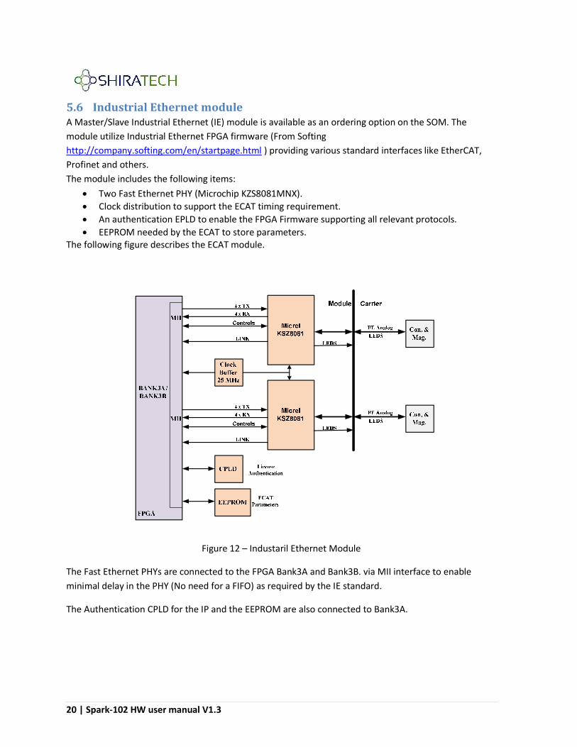
5.6 Industrial Ethernet module A Master/Slave Industrial Ethernet (IE) module is available as an ordering option on the SOM. The
module utilize Industrial Ethernet FPGA firmware (From Softing
http://company.softing.com/en/startpage.html ) providing various standard interfaces like EtherCAT,
Profinet and others.
The module includes the following items:
Two Fast Ethernet PHY (Microchip KZS8081MNX).
Clock distribution to support the ECAT timing requirement.
An authentication EPLD to enable the FPGA Firmware supporting all relevant protocols.
EEPROM needed by the ECAT to store parameters. The following figure describes the ECAT module.
Figure 12 – Industaril Ethernet Module
The Fast Ethernet PHYs are connected to the FPGA Bank3A and Bank3B. via MII interface to enable
minimal delay in the PHY (No need for a FIFO) as required by the IE standard.
The Authentication CPLD for the IP and the EEPROM are also connected to Bank3A.

21 | Spark-102 HW user manual V1.3
BANK Diff. Pair Pin Description
VREFB3BN0 DIFFIO_RX_B26n AE9 CPLD_CLK_SHIFT
VREFB3BN0 DIFFIO_RX_B26p AD10 CPLD_CHAL_VAL
VREFB3BN0 DIFFIO_RX_B30n AE11 CPLD_CHAL_DATA
VREFB3BN0 DIFFIO_RX_B30p AD11 CPLD_RESP_VALID
VREFB3BN0 DIFFIO_RX_B38n AD12 CPLD_RESP_DATA
VREFB3BN0 DIFFIO_RX_B38p AE12 CPLD_RST_SYSTEM_n
VREFB3BN0 DIFFIO_RX_B27n U11 ECAT_I2C DATA
VREFB3BN0 DIFFIO_RX_B27p T11 ECAT_I2C CLK
VREFB3BN0 DIFFIO_TX_B25n AF4 PHY1 TXD0
VREFB3BN0 DIFFIO_TX_B32p AF5 PHY1 TXD1
VREFB3BN0 DIFFIO_TX_B32n AF6 PHY1 TXD2
VREFB3BN0 DIFFIO_TX_B33p AF7 PHY1 TXD3
VREFB3BN0 DIFFIO_TX_B25p AE4 PHY1 TX_CLK
VREFB3BN0 DIFFIO_TX_B28p AE7 PHY1 TX_EN
VREFB3BN0 DIFFIO_TX_B36n AH2 PHY1 RXD0
VREFB3BN0 DIFFIO_TX_B36p AH3 PHY1 RXD1
VREFB3BN0 DIFFIO_TX_B37n AH4 PHY1 RXD2
VREFB3BN0 DIFFIO_TX_B40p AH6 PHY1 RXD3
VREFB3BN0 DIFFIO_TX_B28n AF8 PHY1 RX_DV
VREFB3BN0 DIFFIO_TX_B29n AF9 PHY1 RX_ER
VREFB3BN0 DIFFIO_TX_B33n AG6 PHY1 RX_CLK
VREFB3BN0 DIFFIO_RX_B34n AF10 PHY1 CRS
VREFB3BN0 DIFFIO_RX_B34p AF11 PHY1 COL
VREFB3BN0 DIFFIO_TX_B29p AE8 PHY1 LINK STATUS
VREFB3AN0 DIFFIO_RX_B1n Y8 PHY2 TXD0
VREFB3AN0 DIFFIO_RX_B1p W8 PHY2 TXD1
VREFB3AN0 DIFFIO_RX_B3n T8 PHY2 TXD2
VREFB3AN0 DIFFIO_RX_B3p U9 PHY2 TXD3
VREFB3AN0 DIFFIO_RX_B5p U10 PHY2 TX_CLK
VREFB3AN0 DIFFIO_RX_B5n V10 PHY2 TX_EN
VREFB3AN0 DIFFIO_TX_B6n AD4 PHY2 RXD0
VREFB3AN0 DIFFIO_TX_B6p AC4 PHY2 RXD1
VREFB3AN0 DIFFIO_TX_B4n AB4 PHY2 RXD2
VREFB3AN0 DIFFIO_TX_B4p AA4 PHY2 RXD3
VREFB3AN0 DIFFIO_TX_B8p AD5 PHY2 RX_DV
VREFB3AN0 DIFFIO_TX_B2p Y5 PHY2 RX_ER
VREFB3AN0 Y4 PHY2 RX_CLK
VREFB3AN0 DIFFIO_RX_B7n AA11 PHY2 CRS
VREFB3AN0 DIFFIO_RX_B7p Y11 PHY2 COL
VREFB3AN0 DIFFIO_TX_B8n AE6 PHY2 LINK STATUS
VREFB3BN0 DIFFIO_RX_B35p T13 FE MDC
VREFB3BN0 DIFFIO_RX_B35n T12 FE MDIO
VREFB3BN0 DIFFIO_TX_B37p AG5 FE_CLKO (25 MHz)
CPLD
EEPROM
Fast Ethernet 1
Fast Ethernet 2
Misc.
The following table provides the pins used for Ethernet connectivity to the FPGA.
Phy Reset and Phy configuration:
After the FPGA is loaded, an active low reset should be asserted to the Phy devices for proper operation. The Phy
reset is provided for both Phy devices. The Phy devices reset should be assigned AG5 of the FPGA for Spark102v1
and to pin AH5 for spark-102v2.
22 | Spark-102 HW user manual V1.3
During reset the phy config pins should be set to '0' (CRS, Collision and RXDV).
5.7 CSEL Configuration There are two signals CSEL0 and CSEL1 that define the FPGA internal clock architecture. These signals
are not available to the user and are defined as default on the SOM.
6 SMARC interface Pin assignment The connector offers 314 pins which are used for:
Power
GPIOs
Fixed interfaces like GE and USB
RFU - unused pins reserved for future use.
The full pin out of the Spark is available in a dedicated document “SPARK pin out definition” available on
the Shiratech web site.
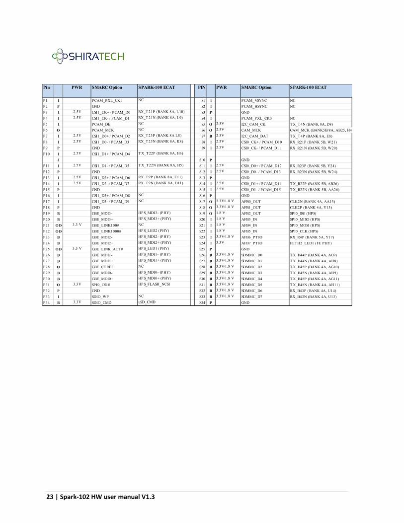
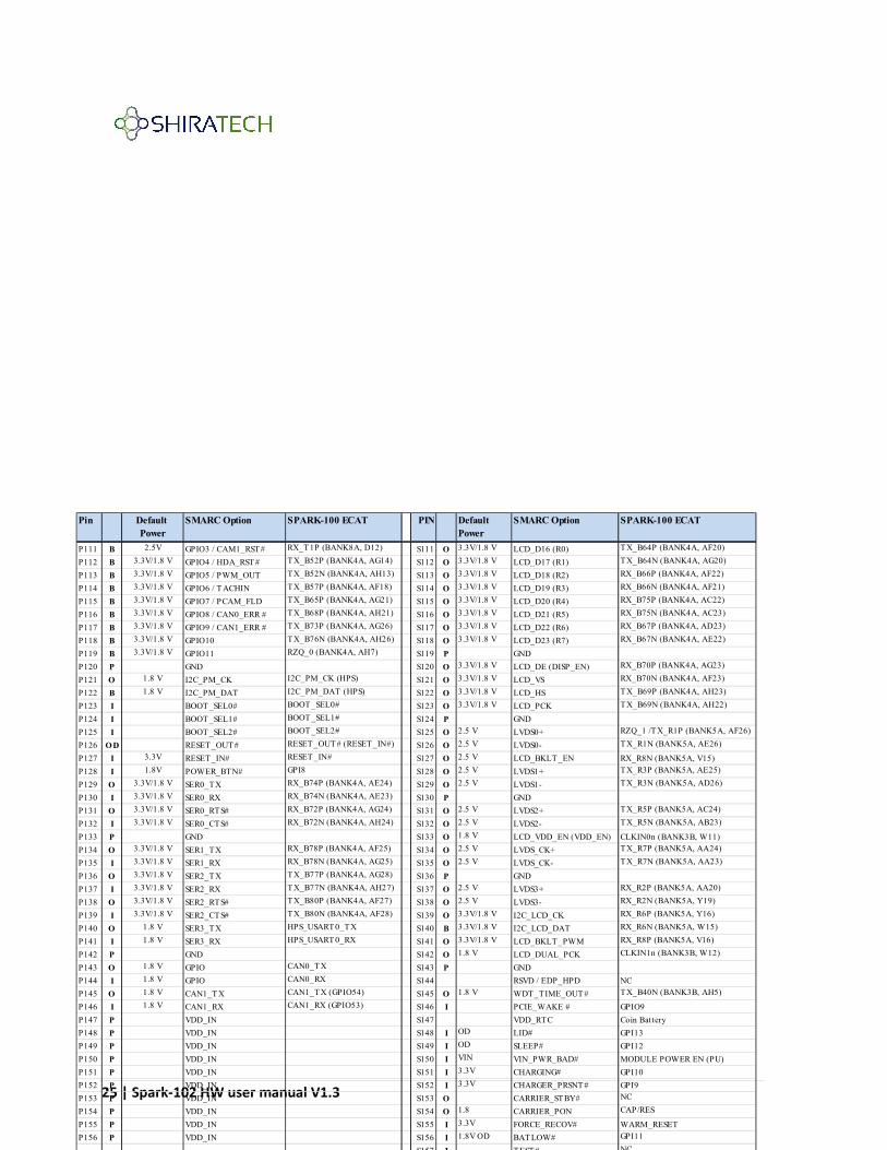
The SPARK-102 supports the SMARC standard connector. The following table describes the pins
allocation, their functionality and there power.
23 | Spark-102 HW user manual V1.3
Pin PWR SMARC Option SPARK-100 ECAT PIN PWR SMARC Option SPARK-100 ECAT
P1 I PCAM_PXL_CK1 NC S1 I PCAM_VSYNC NC
P2 P GND S2 I PCAM_HSYNC NC
P3 I 2.5V CSI1_CK+ / PCAM_D0 RX_T21P (BANK 8A, L10) S3 P GND
P4 I 2.5V CSI1_CK- / PCAM_D1 RX_T21N (BANK 8A, L9) S4 I PCAM_PXL_CK0 NC
P5 I PCAM_DE NC S5 O 2.5V I2C_CAM_CK T X_T4N (BANK 8A, D8)
P6 O PCAM_MCK NC S6 O 2.5V CAM_MCK CAM_MCK (BANK5B/8A, AB25, H4)
P7 I 2.5V CSI1_D0+ / PCAM_D2 RX_T23P (BANK 8A L8) S7 B 2.5V I2C_CAM_DAT T X_T4P (BANK 8A, E8)
P8 I 2.5V CSI1_D0- / PCAM_D3 RX_T23N (BANK 8A, K8) S8 I 2.5V CSI0_CK+ / PCAM_D10 RX_R21P (BANK 5B, W21)
P9 P GND S9 I 2.5V CSI0_CK- / PCAM_D11 RX_R21N (BANK 5B, W20)
P10 I 2.5V CSI1_D1+ / PCAM_D4 T X_T 22P (BANK 8A, H6)
J S10 P GND
P11 I 2.5V CSI1_D1- / PCAM_D5 T X_T 22N (BANK 8A, H5) S11 I 2.5V CSI0_D0+ / PCAM_D12 RX_R23P (BANK 5B, Y24)
P12 P GND S12 I 2.5V CSI0_D0- / PCAM_D13 RX_R23N (BANK 5B, W24)
P13 I 2.5V CSI1_D2+ / PCAM_D6 RX_T9P (BANK 8A, E11) S13 P GND
P14 I 2.5V CSI1_D2- / PCAM_D7 RX_T9N (BANK 8A, D11) S14 I 2.5V CSI0_D1+ / PCAM_D14 T X_R22P (BANK 5B, AB26)
P15 P GND S15 I 2.5V CSI0_D1- / PCAM_D15 T X_R22N (BANK 5B, AA26)
P16 I CSI1_D3+ / PCAM_D8 NC S16 P GND
P17 I CSI1_D3- / PCAM_D9 NC S17 O 3.3V/1.8 V AFB0_OUT CLK2N (BANK 4A, AA13)
P18 P GND S18 O 3.3V/1.8 V AFB1_OUT CLK2P (BANK 4A, Y13)
P19 B GBE_MDI3- HPS_MDI3- (PHY) S19 O 1.8 V AFB2_OUT SPI0_SS0 (HPS)
P20 B GBE_MDI3+ HPS_MDI3+ (PHY) S20 I 1.8 V AFB3_IN SPI0_MISO (HPS)
P21 O D 3.3 V GBE_LINK100# NC S21 I 1.8 V AFB4_IN SPI0_MOSI (HPS)
P22 O D GBE_LINK1000# HPS_LED2 (PHY) S22 I 1.8 V AFB5_IN SPI0_CLK (HPS)
P23 B GBE_MDI2- HPS_MDI2- (PHY) S23 I 3.3V/1.8 V AFB6_PT IO RX_R4P (BANK 5A, Y17)
P24 B GBE_MDI2+ HPS_MDI2+ (PHY) S24 I 3.3V AFB7_PT IO FETH2_LED1 (FE PHY)
P25 O D 3.3 V GBE_LINK_ACT # HPS_LED1 (PHY) S25 P GND
P26 B GBE_MDI1- HPS_MDI1- (PHY) S26 B 3.3V/1.8 V SDMMC_D0 T X_B44P (BANK 4A, AG9)
P27 B GBE_MDI1+ HPS_MDI1+ (PHY) S27 B 3.3V/1.8 V SDMMC_D1 T X_B44N (BANK 4A, AH8)
P28 O GBE_CT REF NC S28 B 3.3V/1.8 V SDMMC_D2 T X_B45P (BANK 4A, AG10)
P29 B GBE_MDI0- HPS_MDI0- (PHY) S29 B 3.3V/1.8 V SDMMC_D3 T X_B45N (BANK 4A, AH9)
P30 B GBE_MDI0+ HPS_MDI0+ (PHY) S30 B 3.3V/1.8 V SDMMC_D4 T X_B48P (BANK 4A, AG11)
P31 O 3.3V SPI0_CS1# HPS_FLASH_NCS1 S31 B 3.3V/1.8 V SDMMC_D5 T X_B48N (BANK 4A, AH11)
P32 P GND S32 B 3.3V/1.8 V SDMMC_D6 RX_B43P (BANK 4A, U14)
P33 I SDIO_WP NC S33 B 3.3V/1.8 V SDMMC_D7 RX_B43N (BANK 4A, U13)
P34 B 3.3V SDIO_CMD uSD_CMD S34 P GND

24 | Spark-102 HW user manual V1.3
Pin Default
Power
SMARC Option SPARK-100 ECAT PIN Default
Power
SMARC Option SPARK-100 ECAT
P35 I SDIO_CD# NC S35 O 3.3V/1.8 V SDMMC_CK RX_B51P (BANK 4A, W14)
P36 O 3.3V SDIO_CK uSD_CLK (HPS) S36 B 3.3V/1.8 V SDMMC_CMD RX_B51N (BANK 4A, V13)
P37 O 3.3V SDIO_PWR_EN SDMMC_PWREN (HPS) S37 O 3.3V/1.8 V SDMMC_RST# RX_B42P (BANK 4A, AG13)
P38 P GND S38 O 3.3V/1.8 V AUDIO_MCK RX_B42N (BANK 4A, AF13)
P39 B 3.3V SDIO_D0 uSD_D0 (HPS) S39 B 3.3V/1.8 V I2S0_LRCK RX_B46P (BANK 4A, AF15)
P40 B 3.3V SDIO_D1 uSD_D1 (HPS) S40 O 3.3V/1.8 V I2S0_SDOUT RX_B46N (BANK 4A, AE15)
P41 B 3.3V SDIO_D2 uSD_D2 (HPS) S41 I 3.3V/1.8 V I2S0_SDIN T X_B53P (BANK 4A, AG15)
P42 B 3.3V SDIO_D3 uSD_D3 (HPS) S42 B 3.3V/1.8 V I2S0_CK T X_B53N (BANK 4A, AH14)
P43 O SPI0_CS0# NC S43 B 2.5V I2S1_LRCK CLK0 (MAIN CLOCK)
P44 O 3.3V SPI0_CK HPS_FLASH_DCLK S44 O I2S1_SDOUT NC
P45 I 3.3V SPI0_DIN HPS_FLASH_DAT A1 S45 I I2S1_SDDIN NC
P46 O 3.3V SPI0_DO HPS_FLASH_DAT A0 S46 B I2S1_CK NC
P47 P GND S47 P GND
P48 O SAT A_TX+ GXB_TX_L5P (F2) S48 O 1.8 V I2C_GP_CK I2C_GP_CK (HPS)
P49 O SAT A_TX- GXB_TX_L5N (F1) S49 B 1.8 V I2C_GP_DAT I2C_GP_DAT (HPS)
P50 P GND S50 B I2S2_LRCK NC
P51 I SAT A_RX+ GXB_RX_L5P (D2) S51 O I2S2_SDOUT NC
P52 I SAT A_RX- GXB_RX_L5N (D1) S52 I I2S2_SDIN NC) NC
P53 P GND S53 B I2S2_CK (NC) NC
P54 O 1.8 V SPI1_CS0# SPI1_SS0 (HPS) S54 O D 3.3V SATA_ACT # GPIO0
P55 O 1.8 V SPI1_CS1# NC S55 3.3V AFB8_PT IO FETH1_LED1 (FE PHY)
P56 O 1.8 V SPI1_CK SPI1_CLK (HPS) S56 2.5V AFB9_PT IO RX_R4N (BANK 5A, Y18)
P57 I 1.8 V SPI1_DIN SPI1_MISO (HPS) S57 PCAM_ON_CSI0# NC
P58 O 1.8 V SPI1_DO SPI1_MOSI (HPS) S58 PCAM_ON_CSI1# NC
P59 P GND S59 O SPDIF_OUT NC
P60 B USB0+ HHSDP_OTG (PHY) S60 I SPDIF_IN NC
P61 B USB0- HHSDM_OT G (PHY) S61 P GND
P62 B 3.3V USB0_EN_OC# USB0_EN_OC# (PHY) S62 B AFB_DIFF0+ FETH1_T X1+ (FE PHY)
P63 I 5V USB0_VBUS_DET USB0_VBUS (PHY) S63 B AFB_DIFF0- FETH1_T X1- (FE PHY)
P64 I 3.3V USB0_OT G_ID USB0_OTG_ID (PHY) S64 P GND
P65 B USB1+ NC S65 B AFB_DIFF1+ FETH1_RX1+ (FE PHY)
P66 B USB1- NC S66 B AFB_DIFF1- FETH1_RX1- (FE PHY)
P67 B USB1_EN_OC# NC S67 P GND
P68 P GND S68 B AFB_DIFF2+ FETH2_T X1+ (FE PHY)
P69 B USB2+ NC S69 B AFB_DIFF2- FETH2_T X1- (FE PHY)
25 | Spark-102 HW user manual V1.3
Pin Default
Power
SMARC Option SPARK-100 ECAT PIN Default
Power
SMARC Option SPARK-100 ECAT
P111 B 2.5V GPIO3 / CAM1_RST # RX_T1P (BANK8A, D12) S111 O 3.3V/1.8 V LCD_D16 (R0) TX_B64P (BANK4A, AF20)
P112 B 3.3V/1.8 V GPIO4 / HDA_RST # TX_B52P (BANK4A, AG14) S112 O 3.3V/1.8 V LCD_D17 (R1) TX_B64N (BANK4A, AG20)
P113 B 3.3V/1.8 V GPIO5 / PWM_OUT TX_B52N (BANK4A, AH13) S113 O 3.3V/1.8 V LCD_D18 (R2) RX_B66P (BANK4A, AF22)
P114 B 3.3V/1.8 V GPIO6 / T ACHIN TX_B57P (BANK4A, AF18) S114 O 3.3V/1.8 V LCD_D19 (R3) RX_B66N (BANK4A, AF21)
P115 B 3.3V/1.8 V GPIO7 / PCAM_FLD TX_B65P (BANK4A, AG21) S115 O 3.3V/1.8 V LCD_D20 (R4) RX_B75P (BANK4A, AC22)
P116 B 3.3V/1.8 V GPIO8 / CAN0_ERR # TX_B68P (BANK4A, AH21) S116 O 3.3V/1.8 V LCD_D21 (R5) RX_B75N (BANK4A, AC23)
P117 B 3.3V/1.8 V GPIO9 / CAN1_ERR # TX_B73P (BANK4A, AG26) S117 O 3.3V/1.8 V LCD_D22 (R6) RX_B67P (BANK4A, AD23)
P118 B 3.3V/1.8 V GPIO10 TX_B76N (BANK4A, AH26) S118 O 3.3V/1.8 V LCD_D23 (R7) RX_B67N (BANK4A, AE22)
P119 B 3.3V/1.8 V GPIO11 RZQ_0 (BANK4A, AH7) S119 P GND
P120 P GND S120 O 3.3V/1.8 V LCD_DE (DISP_EN) RX_B70P (BANK4A, AG23)
P121 O 1.8 V I2C_PM_CK I2C_PM_CK (HPS) S121 O 3.3V/1.8 V LCD_VS RX_B70N (BANK4A, AF23)
P122 B 1.8 V I2C_PM_DAT I2C_PM_DAT (HPS) S122 O 3.3V/1.8 V LCD_HS TX_B69P (BANK4A, AH23)
P123 I BOOT _SEL0# BOOT _SEL0# S123 O 3.3V/1.8 V LCD_PCK TX_B69N (BANK4A, AH22)
P124 I BOOT _SEL1# BOOT _SEL1# S124 P GND
P125 I BOOT _SEL2# BOOT _SEL2# S125 O 2.5 V LVDS0+ RZQ_1 /TX_R1P (BANK5A, AF26)
P126 O D RESET_OUT # RESET_OUT # (RESET_IN#) S126 O 2.5 V LVDS0- TX_R1N (BANK5A, AE26)
P127 I 3.3V RESET_IN# RESET_IN# S127 O 2.5 V LCD_BKLT_EN RX_R8N (BANK5A, V15)
P128 I 1.8V POWER_BTN# GPI8 S128 O 2.5 V LVDS1+ TX_R3P (BANK5A, AE25)
P129 O 3.3V/1.8 V SER0_TX RX_B74P (BANK4A, AE24) S129 O 2.5 V LVDS1- TX_R3N (BANK5A, AD26)
P130 I 3.3V/1.8 V SER0_RX RX_B74N (BANK4A, AE23) S130 P GND
P131 O 3.3V/1.8 V SER0_RTS# RX_B72P (BANK4A, AG24) S131 O 2.5 V LVDS2+ TX_R5P (BANK5A, AC24)
P132 I 3.3V/1.8 V SER0_CTS# RX_B72N (BANK4A, AH24) S132 O 2.5 V LVDS2- TX_R5N (BANK5A, AB23)
P133 P GND S133 O 1.8 V LCD_VDD_EN (VDD_EN) CLKIN0n (BANK3B, W11)
P134 O 3.3V/1.8 V SER1_TX RX_B78P (BANK4A, AF25) S134 O 2.5 V LVDS_CK+ TX_R7P (BANK5A, AA24)
P135 I 3.3V/1.8 V SER1_RX RX_B78N (BANK4A, AG25) S135 O 2.5 V LVDS_CK- TX_R7N (BANK5A, AA23)
P136 O 3.3V/1.8 V SER2_TX TX_B77P (BANK4A, AG28) S136 P GND
P137 I 3.3V/1.8 V SER2_RX TX_B77N (BANK4A, AH27) S137 O 2.5 V LVDS3+ RX_R2P (BANK5A, AA20)
P138 O 3.3V/1.8 V SER2_RTS# TX_B80P (BANK4A, AF27) S138 O 2.5 V LVDS3- RX_R2N (BANK5A, Y19)
P139 I 3.3V/1.8 V SER2_CTS# TX_B80N (BANK4A, AF28) S139 O 3.3V/1.8 V I2C_LCD_CK RX_R6P (BANK5A, Y16)
P140 O 1.8 V SER3_TX HPS_USART 0_TX S140 B 3.3V/1.8 V I2C_LCD_DAT RX_R6N (BANK5A, W15)
P141 I 1.8 V SER3_RX HPS_USART 0_RX S141 O 3.3V/1.8 V LCD_BKLT_PWM RX_R8P (BANK5A, V16)
P142 P GND S142 O 1.8 V LCD_DUAL_PCK CLKIN1n (BANK3B, W12)
P143 O 1.8 V GPIO CAN0_TX S143 P GND
P144 I 1.8 V GPIO CAN0_RX S144 RSVD / EDP_HPD NC
P145 O 1.8 V CAN1_T X CAN1_TX (GPIO54) S145 O 1.8 V WDT_TIME_OUT # TX_B40N (BANK3B, AH5)
P146 I 1.8 V CAN1_RX CAN1_RX (GPIO53) S146 I PCIE_WAKE # GPIO9
P147 P VDD_IN S147 VDD_RTC Coin Battery
P148 P VDD_IN S148 I OD LID# GPI13
P149 P VDD_IN S149 I OD SLEEP# GPI12
P150 P VDD_IN S150 I VIN VIN_PWR_BAD# MODULE POWER EN (PU)
P151 P VDD_IN S151 I 3.3V CHARGING# GPI10
P152 P VDD_IN S152 I 3.3V CHARGER_PRSNT # GPI9
P153 P VDD_IN S153 O CARRIER_STBY# NC
P154 P VDD_IN S154 O 1.8 CARRIER_PON CAP/RES
P155 P VDD_IN S155 I 3.3V FORCE_RECOV# WARM_RESET
P156 P VDD_IN S156 I 1.8V OD BAT LOW# GPI11
S157 I TEST # NC

26 | Spark-102 HW user manual V1.3
Pin Default
Power
SMARC Option SPARK-100 ECAT PIN Default
Power
SMARC Option SPARK-100 ECAT
P70 B USB2- NC S70 P GND
P71 B USB2_EN_OC# NC S71 B AFB_DIFF3+ FETH2_RX1+ (FE PHY)
P72 I PCIE_C_PRSNT # NC S72 B AFB_DIFF3- FETH2_RX1- (FE PHY)
P73 I PCIE_B_PRSNT # NC S73 P GND
P74 I PCIE_A_PRSNT # NC S74 B 3.3V/1.8 V AFB_DIFF4+ CLK3P (BANK 4A, Y15)
S75 B 3.3V/1.8 V AFB_DIFF4- CLK3N (BANK 4A, AA15)
P75 O PCIE_A_RST# NC
P76 I PCIE_C_CKREQ# NC S76 O PCIE_B_RST# NC
P77 I PCIE_B_CKREQ# NC S77 O PCIE_C_RST# NC
P78 I PCIE_A_CKREQ# NC S78 I PCIE_C_RX+ GXB_RX_L4P (K2)
P79 P GND S79 I PCIE_C_RX- GXB_RX_L4N K1)
P80 O PCIE_C_REFCK NC S80 P GND
P81 O PCIE_C_REFCK NC S81 O PCIE_C_TX+ GXB_TX_L4P (H2)
P82 P GND S82 O PCIE_C_TX- GXB_TX_L4N (H1)
P83 O PCIE_A_REFCK+ GXB_CLK0LP (V5) S83 P GND
P84 O PCIE_A_REFCK- GXB_CLK0LN (V4) S84 O PCIE_B_REFCK+ GXB_CLK1LP (P8)
P85 P GND S85 O PCIE_B_REFCK- GXB_CLK1LN (N8)
P86 I PCIE_A_RX+ GXB_RX_L1P (AB2) S86 P GND
P87 I PCIE_A_RX- GXB_RX_L1N (AB1) S87 I PCIE_B_RX+ GXB_RX_L3P (P2)
P88 P GND S88 I PCIE_B_RX- GXB_RX_L3N (P1)
P89 O PCIE_A_TX+ GXB_T X_L1P (Y2) S89 P GND
P90 O PCIE_A_TX- GXB_T X_L1N (Y1) S90 O PCIE_B_TX+ GXB_TX_L3P (M2)
P91 P GND S91 O PCIE_B_TX- GXB_TX_L3N (M1)
P92 O HDMI_D2+ GXB_RX_L2P (V2) S92 P GND
P93 O HDMI_D2- GXB_RX_L2N (V1) S93 O 3.3V/1.8 V LCD_D0 (B0) RX_B50P (BANK4A, AF17)
P94 P GND S94 O 3.3V/1.8 V LCD_D1 (B1) RX_B50N (BANK4A, AG16)
P95 O HDMI_D1+ GXB_T X_L2P (T2) S95 O 3.3V/1.8 V LCD_D2 (B2) RX_B54P (BANK4A, AD17)
P96 O HDMI_D1- GXB_T X_L2N (T 1) S96 O 3.3V/1.8 V LCD_D3 (B3) RX_B54N (BANK4A, AE17)
P97 P GND S97 O 3.3V/1.8 V LCD_D4 (B4) T X_B56P (BANK4A, AH17)
P98 O HDMI_D0+ GXB_RX_L0P (AF2) S98 O 3.3V/1.8 V LCD_D5 (B5) T X_B56N (BANK4A, AH16)
P99 O HDMI_D0- GXB_RX_L0N (AF1) S99 O 3.3V/1.8 V LCD_D6 (B6) T X_B60P (BANK4A, AG18)
P100 P GND S100 O 3.3V/1.8 V LCD_D7 (B7) T X_B60N (BANK4A, AH18)
P101 O HDMI_CK+ GXB_T X_L0P (AD2) S101 P GND
P102 O HDMI_CK- GXB_T X_L0N (AD1) S102 O 3.3V/1.8 V LCD_D8 (G0) RX_B59P (BANK4A, AA19)
P103 P GND S103 O 3.3V/1.8 V LCD_D9 (G1) RX_B59N (BANK4A, AA18)
P104 I HDMI_HPD MSEL0 S104 O 3.3V/1.8 V LCD_D10 (G2) RX_B58P (BANK4A, AE19)
P105 O HDMI_CTRL_CK MSEL1 S105 O 3.3V/1.8 V LCD_D11 (G3) RX_B58N (BANK4A, AD19)
P106 B HDMI_CTRL_DAT BANK4A VCCIO SEL S106 O 3.3V/1.8 V LCD_D12 (G4) T X_B61P (BANK4A, AG19)
P107 B HDMI_CEC NC S107 O 3.3V/1.8 V LCD_D13 (G5) T X_B61N (BANK4A, AH19)
P108 B 3.3V/1.8 V GPIO0 / CAM0_PWR# TX_B41P (BANK4A, AG8) S108 O 3.3V/1.8 V LCD_D14 (G6) RX_B62P (BANK4A, AE20)
P109 B 3.3V/1.8 V GPIO1 / CAM1_PWR# TX_B49P (BANK4A, AH12) S109 O 3.3V/1.8 V LCD_D15 (G7) RX_B62N (BANK4A, AD20)
P110 B 2.5V GPIO2 / CAM0_RST# RX_T 1N (BANK8A, C12) S110 P GND
27 | Spark-102 HW user manual V1.3
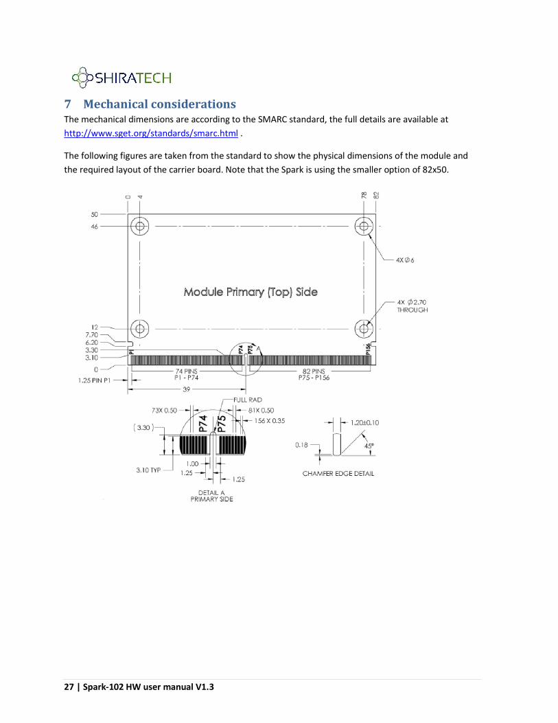
7 Mechanical considerationsThe mechanical dimensions are according to the SMARC standard, the full details are available at
http://www.sget.org/standards/smarc.html
The following figures are taken from the standard to show the physical dimensions of
the required layout of the carrier board. Note that the Spark is using the
V1.3
Mechanical considerations are according to the SMARC standard, the full details are available at
http://www.sget.org/standards/smarc.html .
The following figures are taken from the standard to show the physical dimensions of the module and
the required layout of the carrier board. Note that the Spark is using the smaller option
are according to the SMARC standard, the full details are available at
the module and
smaller option of 82x50.
28 | Spark-102 HW user manual V1.3
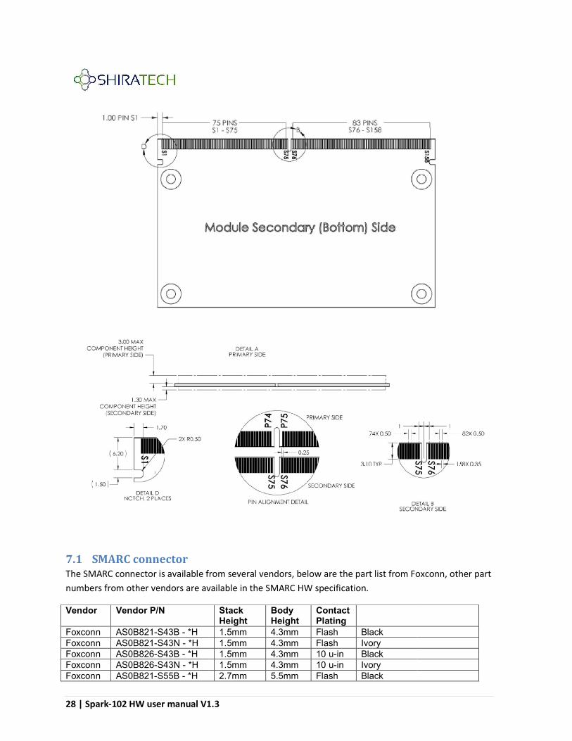
7.1 SMARC connector The SMARC connector is available from several vendors, below are the part list from Foxconn, other part
numbers from other vendors are available in the SMARC HW specification.
Vendor Vendor P/N
Foxconn AS0B821-S43B - *H Foxconn AS0B821-S43N - *H Foxconn AS0B826-S43B - *H Foxconn AS0B826-S43N - *H Foxconn AS0B821-S55B - *H
V1.3
The SMARC connector is available from several vendors, below are the part list from Foxconn, other part
m other vendors are available in the SMARC HW specification.
Stack Height
Body Height
Contact Plating
1.5mm 4.3mm Flash Black 1.5mm 4.3mm Flash Ivory 1.5mm 4.3mm 10 u-in Black 1.5mm 4.3mm 10 u-in Ivory 2.7mm 5.5mm Flash Black
The SMARC connector is available from several vendors, below are the part list from Foxconn, other part
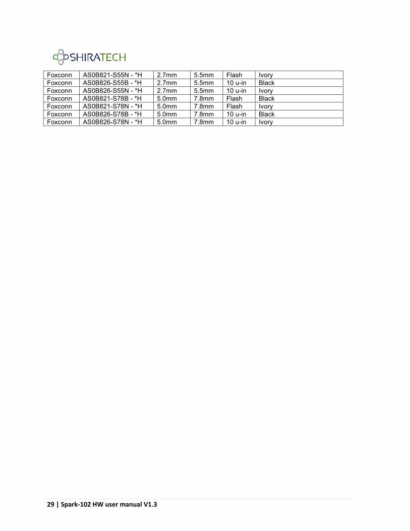
29 | Spark-102 HW user manual V1.3
Foxconn AS0B821-S55N - *H 2.7mm 5.5mm Flash Ivory Foxconn AS0B826-S55B - *H 2.7mm 5.5mm 10 u-in Black Foxconn AS0B826-S55N - *H 2.7mm 5.5mm 10 u-in Ivory Foxconn AS0B821-S78B - *H 5.0mm 7.8mm Flash Black Foxconn AS0B821-S78N - *H 5.0mm 7.8mm Flash Ivory Foxconn AS0B826-S78B - *H 5.0mm 7.8mm 10 u-in Black Foxconn AS0B826-S78N - *H 5.0mm 7.8mm 10 u-in Ivory

30 | Spark-102 HW user manual V1.3
Appendix 1 - Hardware devices used on the SOM
Chip Vendor Details MT29F1G01AAADD Micron NOR Flash Memory - Serial Peripheral Interface (SPI)
TXS02612 TI SDIO port expander with voltage level translation
AT24C01C Atmel I2C-Compatible (2-wire) Serial EEPROM 1-Kbit (128 x 8)
USB3300 Microchip High speed USB host device or OTG phy
TMP108 TI Low Power Digital Temperature Sensor With Two-Wire Serial Interface in WCSP
KSZ9031RN
Micrel 1G Ethernet Physical layer chip
KSZ8081MNXCA Micrel 10/100 Ethernet Physical layer chip (Used for Industrial Ethernet)
24LC16BT Microchip EEPROM for EtherCAT
M570F11NCA Altera Authentication CPLD
31 | Spark-102 HW user manual V1.3
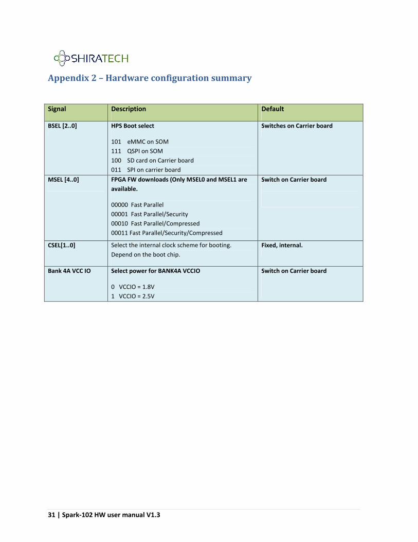
Appendix 2 – Hardware configuration summary
Signal Description Default
BSEL [2..0] HPS Boot select
101 eMMC on SOM
111 QSPI on SOM
100 SD card on Carrier board
011 SPI on carrier board
Switches on Carrier board
MSEL [4..0] FPGA FW downloads (Only MSEL0 and MSEL1 are
available.
00000 Fast Parallel
00001 Fast Parallel/Security
00010 Fast Parallel/Compressed
00011 Fast Parallel/Security/Compressed
Switch on Carrier board
CSEL[1..0] Select the internal clock scheme for booting.
Depend on the boot chip.
Fixed, internal.
Bank 4A VCC IO Select power for BANK4A VCCIO
0 VCCIO = 1.8V
1 VCCIO = 2.5V
Switch on Carrier board
32 | Spark-102 HW user manual V1.3
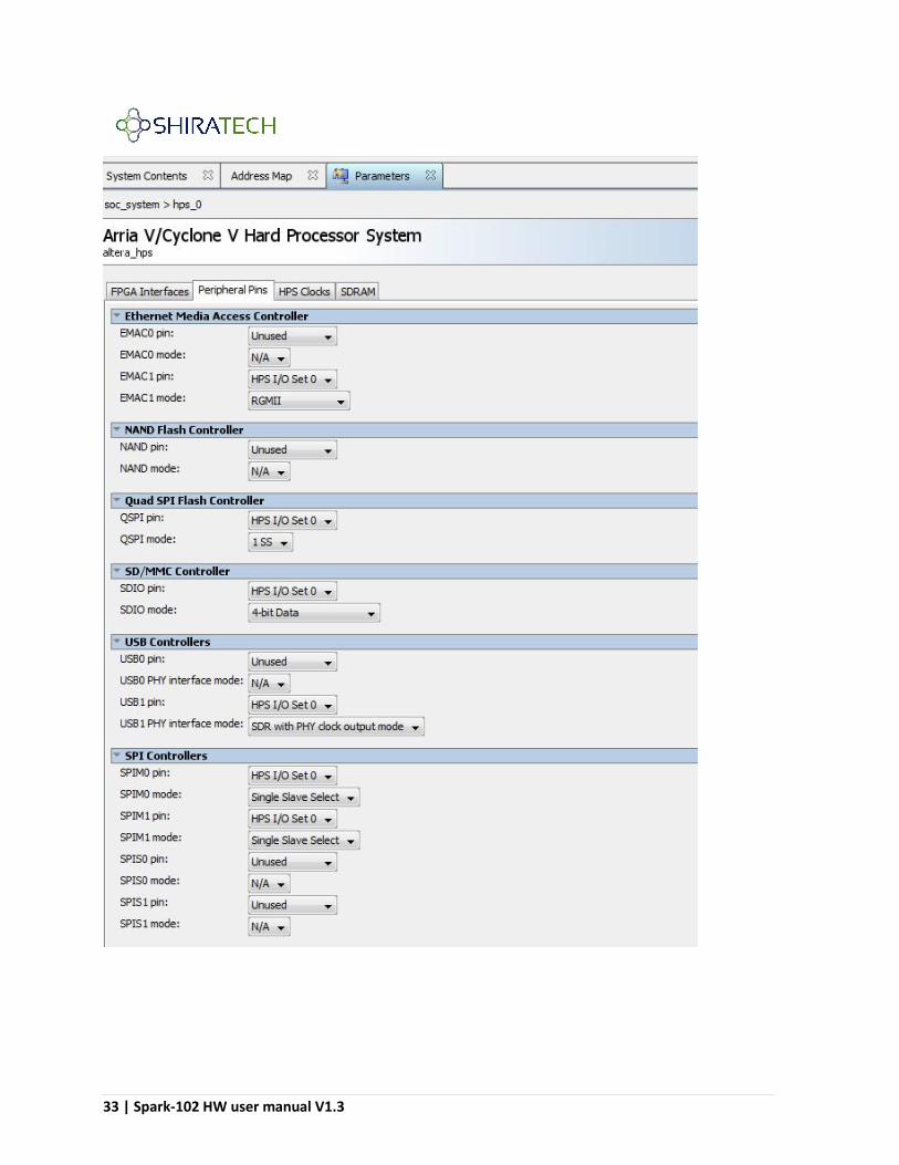
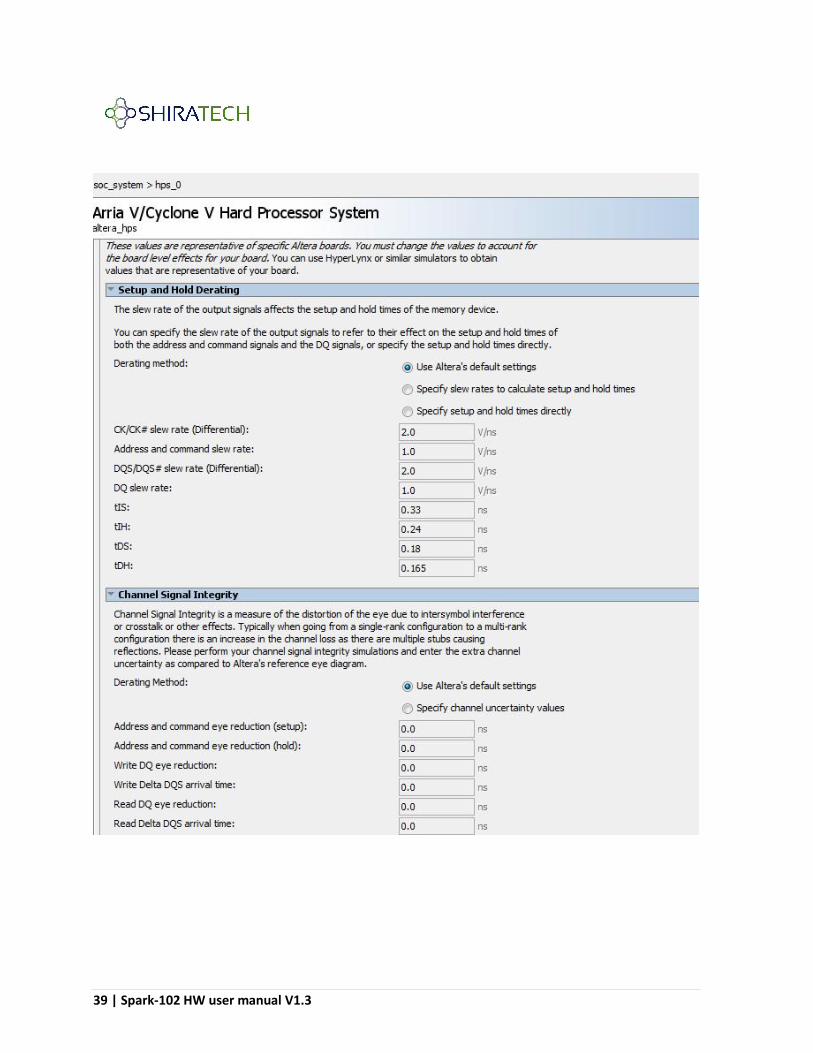
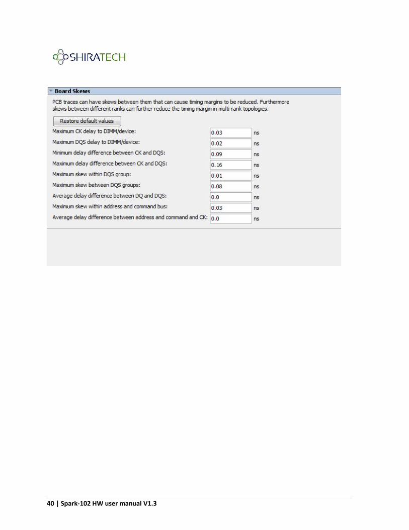
Appendix 3 – Qsys parameters for the Spark The following paragraph provides the HPS configuration used in the demo version provided for the
Spark.
33 | Spark-102 HW user manual V1.3

34 | Spark-102 HW user manual V1.3
The user can modify the configuration according to need. Care must be taken for interfaces which are
connected to hardware devices located on the module like USB, GE, I2C etc…
For interfaces which are connected directly connected to Spark interface, the configuration is open, can
should be taken to the power level provided to these interfaces.

35 | Spark-102 HW user manual V1.3
Clock configuration:
36 | Spark-102 HW user manual V1.3
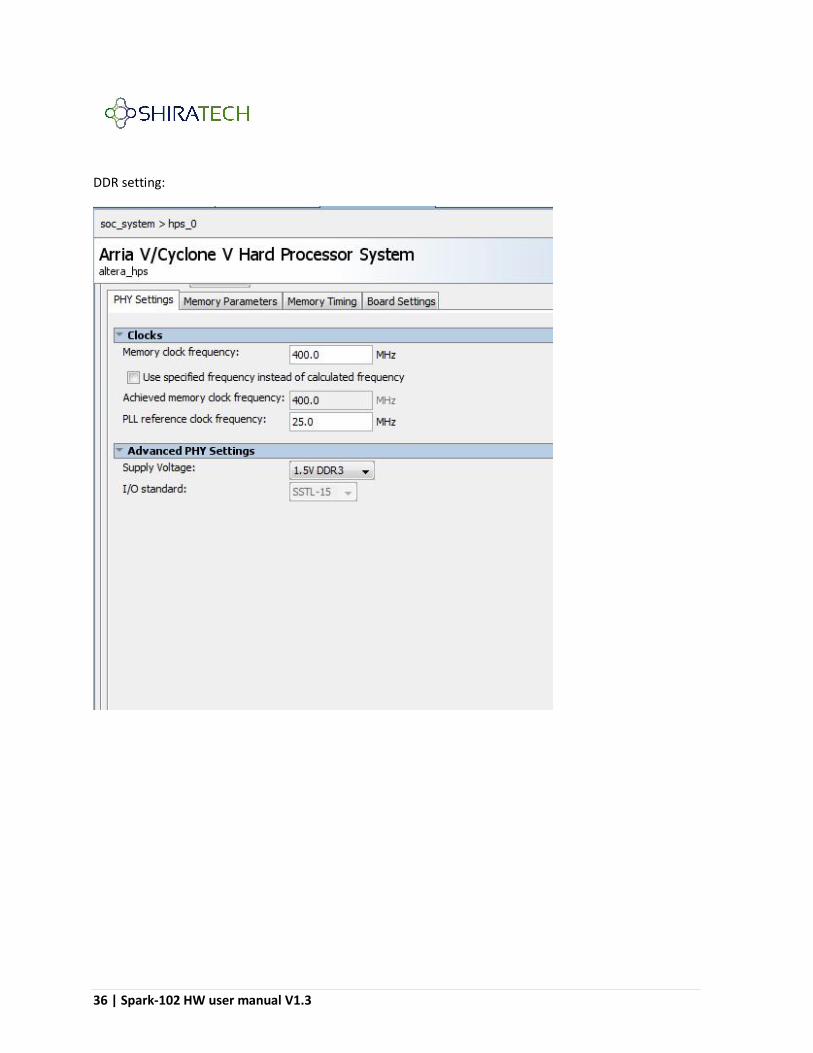
DDR setting:

37 | Spark-102 HW user manual V1.3

38 | Spark-102 HW user manual V1.3
39 | Spark-102 HW user manual V1.3
40 | Spark-102 HW user manual V1.3


