2002 Microchip Technology Inc. DS00823A-page 1 AN823 INTRODUCTION The purpose of this Application Note is to familiarize engineers with PIC16C78X design considerations, specifically: • Potential noise problems in mixed signal design • Features and performance of the new analog/digi- tal peripherals • Some common applications for the PIC16C78X The PIC16C781 and PIC16C782 are the first devices in a new line of mixed analog/digital microcontrollers from Microchip. These microcontrollers are a marriage of our traditional microcontroller architecture with new mixed signal peripherals that change many of the old conventions of embedded microcontroller design. Not only do the new peripherals open up new applications for the microcontroller, they bring new design concerns that might be unfamiliar to traditional microcontroller designers. This Application Note will highlight some of the common problems associated with mixed signal design and offer techniques for overcoming these prob- lems. It will also cover the features and performance of the new peripherals. Finally, this Application Note cov- ers some of the common applications that take advan- tage of the PIC16C78X's unique peripherals. NOISE AND MIXED SIGNAL DESIGN The first area to cover concerning mixed signal design is identifying and controlling potential noise sources. Traditionally, microcontroller designs have enjoyed rel- ative immunity to noise concerns, due to their high noise margins (typically measured in tenths of volts). However, the addition of analog blocks designed to handle low level signals change some of the design pri- orities. Noise levels in the millivolt and microvolt range can now have a significant impact on the performance of the system. Therefore, it is important that the designer acquires new tools and techniques for control- ling, and where possible, eliminating noise. IDENTIFYING NOISE SOURCES Identifying potential noise sources in a design is the first step in controlling or eliminating noise in a mixed signal design. Almost any active circuit in a design can generate noise; however, some circuits are more likely to become noise generators than others. The following is a short list of common sources of noise: 1. Oscillators: This one is an obvious source of periodic AC noise. However, designers should remember that oscillators also have output driv- ers which can generate fast rise time transients and ringing that is unrelated to the oscillator fre- quency. 2. High current/power drive circuits: Another source of fast rise time transients and ringing. 3. Amplifiers/Comparators: The amplifier can become unstable driving capacitive loads. Amplifiers and comparators can oscillate if their bypass capacitors are missing or inadequate. 4. Switching power supply circuits: These circuits can be significant sources of noise because they incorporate both oscillators and high drive cur- rents. 5. Circuits with external connections: These cir- cuits are subject to not only the noise sources inside the cabinet, but also all the external sources including ESD and RFI. 6. Fast rise time logic: Any logic device with a rise time of less than 5-10 nanoseconds is capable of generating noise in the 1 to 100 MHz range. This list is by no means complete. There are other cir- cuits and systems in any design which may be a poten- tial source of noise. However, a good general rule of thumb is: ‘If it is high speed, high power, or is not bypassed correctly, it can generate noise.’ Author: Keith Curtis Microchip Technology Inc. Analog Design in a Digital World Using Mixed Signal Controllers
Transcript
AN823Analog Design in a Digital World Using Mixed Signal Controllers
INTRODUCTION
The purpose of this Application Note is to familiarizeengineers with PIC16C78X design considerations,specifically:
• Potential noise problems in mixed signal design
• Features and performance of the new analog/digi-tal peripherals
• Some common applications for the PIC16C78X
The PIC16C781 and PIC16C782 are the first devices ina new line of mixed analog/digital microcontrollers fromMicrochip. These microcontrollers are a marriage ofour traditional microcontroller architecture with newmixed signal peripherals that change many of the oldconventions of embedded microcontroller design. Notonly do the new peripherals open up new applicationsfor the microcontroller, they bring new design concernsthat might be unfamiliar to traditional microcontrollerdesigners. This Application Note will highlight some ofthe common problems associated with mixed signaldesign and offer techniques for overcoming these prob-lems. It will also cover the features and performance ofthe new peripherals. Finally, this Application Note cov-ers some of the common applications that take advan-tage of the PIC16C78X's unique peripherals.
NOISE AND MIXED SIGNAL DESIGN
The first area to cover concerning mixed signal designis identifying and controlling potential noise sources.Traditionally, microcontroller designs have enjoyed rel-ative immunity to noise concerns, due to their highnoise margins (typically measured in tenths of volts).However, the addition of analog blocks designed tohandle low level signals change some of the design pri-orities. Noise levels in the millivolt and microvolt rangecan now have a significant impact on the performanceof the system. Therefore, it is important that thedesigner acquires new tools and techniques for control-ling, and where possible, eliminating noise.
IDENTIFYING NOISE SOURCES
Identifying potential noise sources in a design is thefirst step in controlling or eliminating noise in a mixedsignal design. Almost any active circuit in a design cangenerate noise; however, some circuits are more likelyto become noise generators than others. The followingis a short list of common sources of noise:
1. Oscillators: This one is an obvious source ofperiodic AC noise. However, designers shouldremember that oscillators also have output driv-ers which can generate fast rise time transientsand ringing that is unrelated to the oscillator fre-quency.
2. High current/power drive circuits: Anothersource of fast rise time transients and ringing.
3. Amplifiers/Comparators: The amplifier canbecome unstable driving capacitive loads.Amplifiers and comparators can oscillate if theirbypass capacitors are missing or inadequate.
4. Switching power supply circuits: These circuitscan be significant sources of noise because theyincorporate both oscillators and high drive cur-rents.
5. Circuits with external connections: These cir-cuits are subject to not only the noise sourcesinside the cabinet, but also all the externalsources including ESD and RFI.
6. Fast rise time logic: Any logic device with a risetime of less than 5-10 nanoseconds is capableof generating noise in the 1 to 100 MHz range.
This list is by no means complete. There are other cir-cuits and systems in any design which may be a poten-tial source of noise. However, a good general rule ofthumb is: ‘If it is high speed, high power, or is notbypassed correctly, it can generate noise.’
Author: Keith CurtisMicrochip Technology Inc.
2002 Microchip Technology Inc. DS00823A-page 1
AN823
Once the noise sources have been identified, the nextstep is to determine if the noise source can be elimi-nated or must be minimized. Obviously, some noisesources (such as oscillators) cannot be removed andmust be minimized. However, other unintentional orundesirable oscillators can often be removed. Some-times small changes made at the beginning of a designcan significantly reduce the probability of noise-relatedproblems. For instance:
1. Verify that all bypass capacitors are present andadequate for their circuits.
2. Verify the load impedance and drive capability ofall amplifiers.
3. Use local linear regulation from an intermediatevoltage to significantly reduce the noise from ahigh power, central switching power supply.
4. Use slower devices in place of fast switchingdevices to reduce the amount of rise time tran-sient related noise.
5. Limit the rise time of faster devices and physi-cally separate the devices and their traces fromsensitive inputs and circuitry.
6. Physically and electrically isolate low level ana-log circuitry from high power drivers to signifi-cantly lower the noise level in the analogcircuitry.
7. Eliminate layout patterns which reinforce electri-cal and magnetic noise fields, such as sharpcorners and loops.
For noise sources that cannot be eliminated, the onlyoption is to isolate sensitive circuitry from the source ofthe noise. In extreme cases, isolation may requireshielding and/or opto-isolation of common signals.However, in most cases, careful design and attention tohow noise travels in a design are sufficient to limit noiseto a manageable level. The following sections willexamine the more common pathways used by noise totravel around a circuit.
ELECTRICAL NOISE PATHS
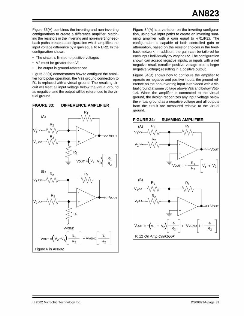
Electrical noise typically travels by one of two methodsof transmission: conducted and radiated.
Conducted noise is defined as noise carried into theaffected circuit by an existing electrical connection inthe design. Typically this is a signal trace, ground trace,or power connection. Conducted noise can be:
• periodic AC noise, repeating AC waveforms• transient, one-shot impulse noise
• DC offset and error voltages• uncorrelated broadband noise from non-switching
devices
Radiated noise, on the other hand, travels as:
• an electrical field• a magnetic field
• an electromagnetic or RF wave
Radiated noise is always transient or periodic AC innature, never DC. Radiated noise is also the more dif-ficult noise source to identify and correct due to its moreintangible path. The following sections cover the morecommon paths that noise follows around a design, plusa collection of tips for controlling the noise.
CONDUCTED NOISE
Conducted electrical noise is, on the other hand, noisewhich travels on the conductors within a design. Thesecret to controlling conducted noise is to identify thepath from the source to the affected circuit and theneither eliminate the source, the path, or both. Whilenoise can travel on any conductor, the more commonpaths are typically the power and ground connections.Power and ground connect to every section of thedesign, making them prime targets for conductednoise. In addition, power and ground carry the supplycurrent needs of the entire circuit, making them thesource of some of the highest power noise as well.Careful attention to the layout of power and groundwithin a mixed signal design is an important step toeliminating many of the conducted noise problems.
A form of conducted noise unique to power and groundconnections is noise generated by the interaction of thetrace's impedance (resistance/inductance) and powersupply currents flowing in the traces. Because bothlines carry current between the power supply and everyactive device in the design, any inductance/resistancein the power and ground is particularly undesirablebecause the impedance will translate the variations inpower supply currents directly into noise voltages. Thismeans that a single power or ground trace will have anoise potential that is the composite of every currentflowing in the trace. This kind of noise can be particu-larly troublesome because the currents in the groundtraces can produce AC, DC, and transient noise.
The noise translates into noise on every signal gener-ated or received by every circuit using the ground tovarious degrees. Therefore, minimizing resistance andinductance in the power supply (particularly in theground trace) is an important design priority. The bestmethod for minimizing impedance of a ground is toreplace discrete ground traces with a ground plane(copper pour).
DS00823A-page 2 2002 Microchip Technology Inc.
AN823
CONDUCTED NOISE: GROUNDS
Copper grounds translate AC and DC currents intoelectrical noise due in part to the finite resistance of thetrace. Copper is a very good conductor, but it doeshave some resistance and that resistance will convertany current flow in the trace into a voltage. Further-more, the current flow in a ground trace will produce arange of ground potentials along the length of the trace.So, when a high current drive output switches at oneend of the trace, it is reasonable to expect that circuitsthat share the ground trace with the driver will experi-ence a shift in the ground potential proportional to thechange in current. Further, if multiple high currentdrives share a common ground, the shift in groundpotential will be a composite of the current flows gener-ating both positive and negative shifts as the differentdrivers switch on and off. The size of the voltage shift,from Ohm’s law, is a function of the change in currentand the impedance (resistance and inductance) of theground path. Therefore, to minimize the effect of highsupply currents, the design must have the minimumground resistance between the drive and the powersupply.
A copper conductor’s resistance is proportional to thelength of the conductor, multiplied by its resistivIty (ρ),divided by the cross sectional area (see Equation 1).From Equation 1 it can be seen that the minimum resis-tance occurs when the conductors length (L) is kept toa minimum and the area (A = width* thickness) of theconductor is at a maximum. Therefore, for minimumground voltage shifts, the ground traces in a mixed sig-nal design should be kept as short and wide as possi-ble. Using thicker copper is also helpful in minimizingtrace impedance, but is often impractical. The optimumsolution is to take the ground width to its maximum bygenerating a ground plane.
EQUATION 1: RESISTANCE EQUATION
While copper grounds translate AC and transient cur-rents into electrical noise due to the copper’s resis-tance, a larger contribution is typically due to theinductance of the ground. Inductance-translated noisevoltages are in response to much smaller AC and tran-sient current flows in a design. The difference in noiseand current is due to the interaction of the frequency ofthe noise current and the inductance of the ground.Higher frequency and faster rise time currents generatelarger noise voltages than lower frequency, slower risetime currents. Unfortunately, each time a digital devicechanges state in the circuit, it generates a currentimpulse in the ground connection of the device. Due tothe higher frequency operation of most digital devices,even a device running at a low frequency will still gen-erate high frequency noise caused by the fast rise time
of the logic. The best option open to the designer tryingto limit high frequency noise is, therefore, to limit theinductance of the ground trace.
A ground trace behaves inductively because, like everyother conductor, it creates a magnetic field in responseto the current flow. The inductance of a trace is depen-dent upon:
• length of the conductor
• configuration (whether straight or coiled)• presence of any ferrous materials in the field
To reduce inductance in a conductor:
1. Keep trace lengths short, eliminating corners.2. As much as is practical, keep traces straight, no
loops.3. Where possible, use non-ferrous materials like
aluminum for cabinets and brackets.
Two circuits that share a common ground with identicalnoise voltages are immune to the Common modeground noise because their ground references areshifting up and down together. If the ground tracebetween two circuits carries little or no current, and thetrace has a minimum of resistance and inductance,then the ground potential of both circuits will be thesame and any common noise present on the groundswill cancel out. This means that if sensitive circuits aregrounded together on an isolated ground (separatefrom high current circuits). The ground carries only aminimal current flow in the trace between the circuits.Therefore, the sensitive circuits will not be significantlyaffected by the high current circuits, even if they ulti-mately share a common power source. The trick is tomake sure that the current flows in the sensitive circuitgrounds are as small as possible and the inductanceand resistance of the ground is kept to an absolute min-imum.
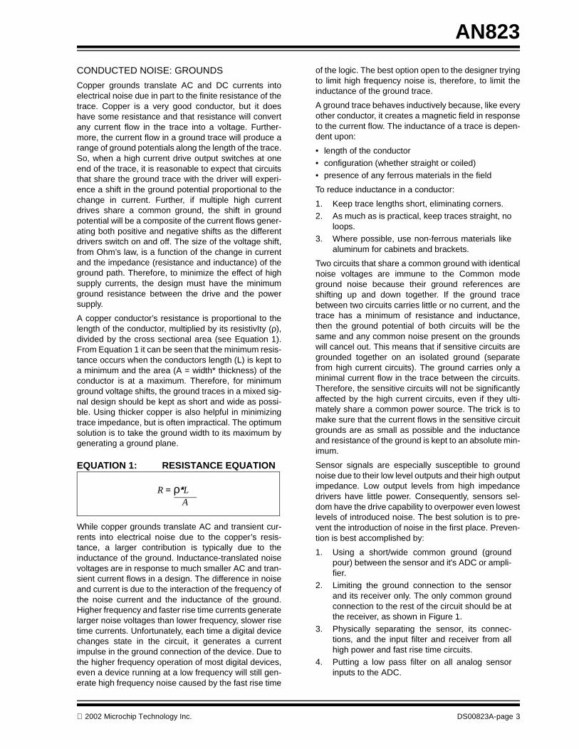
Sensor signals are especially susceptible to groundnoise due to their low level outputs and their high outputimpedance. Low output levels from high impedancedrivers have little power. Consequently, sensors sel-dom have the drive capability to overpower even lowestlevels of introduced noise. The best solution is to pre-vent the introduction of noise in the first place. Preven-tion is best accomplished by:
1. Using a short/wide common ground (groundpour) between the sensor and it's ADC or ampli-fier.
2. Limiting the ground connection to the sensorand its receiver only. The only common groundconnection to the rest of the circuit should be atthe receiver, as shown in Figure 1.
3. Physically separating the sensor, its connec-tions, and the input filter and receiver from allhigh power and fast rise time circuits.
4. Putting a low pass filter on all analog sensorinputs to the ADC.
R = ρ*LA
2002 Microchip Technology Inc. DS00823A-page 3
AN823
FIGURE 1: SENSOR GROUNDS
To summarize, grounds are especially sensitive tonoise due their function as the 0V reference in a circuit,and the presence of all the circuit ground currents. Thebest prevention for noise on the ground return is to:
• keep all ground traces short and wide (ground plane)
• isolate high current drives on separate ground returns
• put sensitive circuits and sensors on their own dedicated ground traces
CONDUCTED NOISE: POWER SUPPLIES
The circuit power supply is another common path forelectrical noise to travel through a mixed signal design.Power supply traces have the same level of connectiv-ity in a circuit as the ground, and are also subject to thesame effects of resistance and inductance, so it is nosurprise that it also acts as a conduit for conductednoise. Therefore, all of the precautions outlined in theprevious section apply equally well to power trace asthey did with grounds. Fortunately, most analogdevices are designed for relative immunity to powersupply noise (the PSRR specification) so the effects ofnoise transmission via the power supply tend to have asmaller overall impact on circuit performance. But becareful, PSRR is no substitute for bypass capacitors.PSRR also drops off with frequency, so PSRR provideslittle or no protection from high frequency noise.
Power supply traces are also different in that they arenot used as the 0V references in the circuit. In manycases (especially in ground referenced applications)variations in supply voltage from device to device donot cause as much of a problem in mixed signaldesigns as do variations in ground potential. Thisopens up some possibilities for filtering and isolation ofnoise that are not possible with ground systems. Spe-cifically, it allows the use of power supply trace's para-sitic inductance as part of a filtering system.
In fact, it can be beneficial to increase a power supplytrace's inductance to further enhance the filtering char-acteristic. Typically, the inductance is increasedthrough the use of Ferrite beads in series with a powerconnection to a device. By placing a Ferrite bead inseries with a power supply connection, the cutoff fre-quency of the filter network is significantly lowered, cut-ting out more of the higher frequency noise. Thecombination of the Ferrite bead and the normal induc-tance of the trace provide the series inductance of thefilter, and the bypass capacitors on the devices andcapacitances in the power supply provide the capaci-tors to ground, creating the low pass filter in Figure 2.
FIGURE 2: POWER SUPPLY PI FILTERING
The result is a network that resists varying currentsflowing through the network, plus a low impedance ACshort to ground on either side. The network provides apath for DC power while creating a barrier to AC andtransient noise. An important note to remember is thatFerrite materials differ in their effectiveness for differentfrequencies. When selecting a Ferrite Bead, it is impor-tant to select a material designed for the noise fre-quency range.
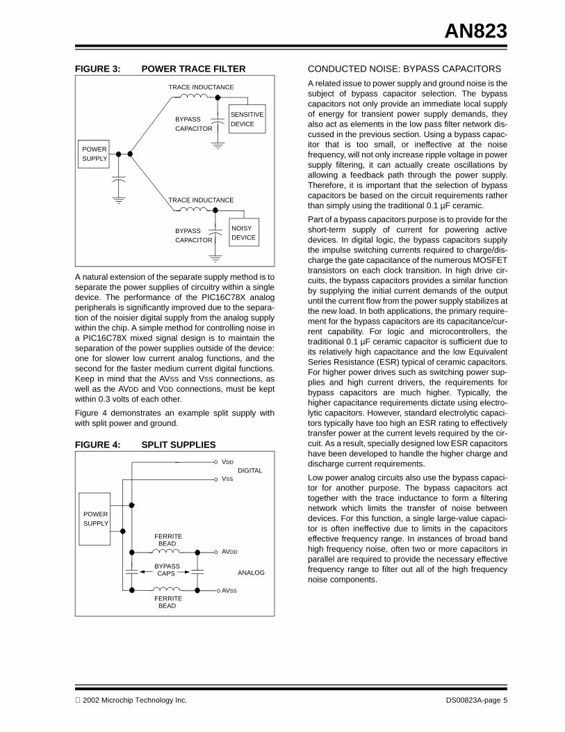
While isolating noisy circuits through the use of induc-tor/capacitor “PI” filters is one of the most effectivemethods for controlling conducted noise on a powersupply trace, a similar (less expensive, but less effec-tive) effect can be achieved by simply separating powersupply traces for different circuits. Separate power sup-ply traces create a similar filter configuration by usingthe natural inductance of the power supply trace as theinductor of the PI network. Although inductance is adesired effect in this configuration, it must be remem-bered that long power traces will also increase thetrace resistance. Separate power traces do, however,have the desirable effect of putting two in-line inductorsand three capacitors to ground between noise and sen-sitive circuits, as shown in Figure 3.
SENSOR 1
SENSOR 2RECEIVER
GROUND CONNECTIONTO THIS END ONLY
PI FILTER
NOISYDEVICE
POWER
SUPPLY
BYPASS CAPACITORS
FERRITE BEAD
SENSITIVEDEVICE
DS00823A-page 4 2002 Microchip Technology Inc.
AN823
FIGURE 3: POWER TRACE FILTER
A natural extension of the separate supply method is toseparate the power supplies of circuitry within a singledevice. The performance of the PIC16C78X analogperipherals is significantly improved due to the separa-tion of the noisier digital supply from the analog supplywithin the chip. A simple method for controlling noise ina PIC16C78X mixed signal design is to maintain theseparation of the power supplies outside of the device:one for slower low current analog functions, and thesecond for the faster medium current digital functions.Keep in mind that the AVSS and VSS connections, aswell as the AVDD and VDD connections, must be keptwithin 0.3 volts of each other.
Figure 4 demonstrates an example split supply withwith split power and ground.
FIGURE 4: SPLIT SUPPLIES
CONDUCTED NOISE: BYPASS CAPACITORS
A related issue to power supply and ground noise is thesubject of bypass capacitor selection. The bypasscapacitors not only provide an immediate local supplyof energy for transient power supply demands, theyalso act as elements in the low pass filter network dis-cussed in the previous section. Using a bypass capac-itor that is too small, or ineffective at the noisefrequency, will not only increase ripple voltage in powersupply filtering, it can actually create oscillations byallowing a feedback path through the power supply.Therefore, it is important that the selection of bypasscapacitors be based on the circuit requirements ratherthan simply using the traditional 0.1 µF ceramic.
Part of a bypass capacitors purpose is to provide for theshort-term supply of current for powering activedevices. In digital logic, the bypass capacitors supplythe impulse switching currents required to charge/dis-charge the gate capacitance of the numerous MOSFETtransistors on each clock transition. In high drive cir-cuits, the bypass capacitors provides a similar functionby supplying the initial current demands of the outputuntil the current flow from the power supply stabilizes atthe new load. In both applications, the primary require-ment for the bypass capacitors are its capacitance/cur-rent capability. For logic and microcontrollers, thetraditional 0.1 µF ceramic capacitor is sufficient due toits relatively high capacitance and the low EquivalentSeries Resistance (ESR) typical of ceramic capacitors.For higher power drives such as switching power sup-plies and high current drivers, the requirements forbypass capacitors are much higher. Typically, thehigher capacitance requirements dictate using electro-lytic capacitors. However, standard electrolytic capaci-tors typically have too high an ESR rating to effectivelytransfer power at the current levels required by the cir-cuit. As a result, specially designed low ESR capacitorshave been developed to handle the higher charge anddischarge current requirements.
Low power analog circuits also use the bypass capaci-tor for another purpose. The bypass capacitors acttogether with the trace inductance to form a filteringnetwork which limits the transfer of noise betweendevices. For this function, a single large-value capaci-tor is often ineffective due to limits in the capacitorseffective frequency range. In instances of broad bandhigh frequency noise, often two or more capacitors inparallel are required to provide the necessary effectivefrequency range to filter out all of the high frequencynoise components.
NOISYDEVICE
SENSITIVE
DEVICE
POWER
SUPPLY
BYPASS
TRACE INDUCTANCE
CAPACITOR
BYPASSCAPACITOR
TRACE INDUCTANCE
POWER
SUPPLY
BYPASS
FERRITE
VDD
VSS
DIGITAL
CAPS
AVDD
AVSS
ANALOG
BEAD
FERRITEBEAD
2002 Microchip Technology Inc. DS00823A-page 5
AN823
The upper frequency limit for a capacitor is expressedby its Self Resonant Frequency (SRF). SRF is definedas the frequency at which the parasitic inductances ofthe capacitor resonate with its capacitance, and is theupper limit of a capacitor’s effective frequency range.Careful selection of a bypass capacitor should includeresearch on the capacitors SRF and the likely frequen-cies of noise that will be present in the design.
The bypass capacitor requirements of different circuitsare dependent upon the functions they will be perform-ing and their tolerance to noise. Care must be taken tochoose bypass capacitors which will be effective in thespecific application.
The PSRR of the analog circuit, the frequency of adja-cent noise sources, and output drive needs of the cir-cuit should be considered in the selection of a bypasscapacitor. In addition, not all capacitors are createdequal. Using a low cost electrolytic capacitor in place ofa low ESR capacitor may seem like a reasonable sub-stitution. However, the losses due to the capacitor'shigher ESR can result in abnormal heating of thecapacitor leading to a rather dramatic failure. Ceramiccapacitors also come in a variety of materials, eachwith its own strengths and weaknesses. X7R ceramiccapacitors are less expensive and are available inmany larger values. However, they also have a lowerSRF which limits their effectiveness against high fre-quency noise. A 1000 pF NPO ceramic capacitor canactually be more effective against 50-100 MHz noisethan a 0.1 µF X7R. Careful selection of a bypasscapacitor up front in the design can save considerabletime in identifying noise problems later on.
As with power supplies and ground traces, the tracelength between a bypass capacitor and its device canhave a significant effect on the bypass capacitor’s per-formance. The bypass capacitor's function is to supplypower and act as a filtering element to remove noise.Adding a resistive/inductance element between thedevice and its bypass capacitor reduces the capacitor’seffectiveness by increasing the capacitor’s parasiticinductance and resistance. The resulting increasedlosses during energy transfers between the capacitorand its device can significantly reduce the capacitor’seffectiveness. Therefore, it is very important that allbypass capacitors must be mounted as close as possi-ble to their devices. The traces connecting the capaci-tor to the device must be kept as short and as wide as
possible to minimize any stray impedance that mightinterfere with the quick, low-loss transfer of energybetween the capacitor and the device.
Unfortunately, the SRF for most capacitor types are notwidely published. To help with this problem, Table 1 isincluded as a guideline with this Application Note thatlists some of the typical SRFs for common types ofcapacitors.
* From page 88 of the “Circuit Designers Companion” by Tim Williams
RADIATED NOISE
Radiated noise is electrical noise which is coupledthrough:
• Electrical fields• Magnetic fields
• Radio frequency energy
Due to its less tangible path, radiated noise can be oneof the most intimidating noise problems to diagnoseand correct. Often, the noise seems to magicallyappear out of thin air. However, once the designerunderstands the basic mechanisms of radiated noise,much of the mystery disappears and the methods foreliminating or controlling the noise problems becomefairly simple. Typically, radiated noise travels via one ormore of a few basic mechanisms:
• Electrostatic discharge (ESD)• Radio Frequency interference (RFI)
The following sections include explanations of the var-ious mechanisms and examples of the more commontechniques for diagnosing the problem as well as rem-edies.
Note: Typically the trace inductance, in combina-tion with the bypass capacitors, is sufficientfor the filtering function. However, if addi-tional filtering is needed for low frequencynoise, it may be necessary to include aninline inductor, or Ferrite Bead, in the sup-ply lead to lower the cut off frequency ofthe filter network.
TABLE 1: SRF FOR COMMON CAPACITORS*
Type Capacitance SRF
Tantalum (chip) 10 µf 600 kHz
Polyester (leaded) 1.0 µf 2 MHz
X7R Ceramic (chip) 0.1 µf 11 MHz
COG/NPO Ceramic (chip) 1000 pF 90 MHz
X7R Ceramic (leaded) 0.1 µf 7 MHz
DS00823A-page 6 2002 Microchip Technology Inc.
AN823
RADIATED NOISE: ELECTROSTATICLY COUPLED NOISE
Electrostatic or Capacitive coupling is electrical noisecoupled from one conductor to another via an electricfield between the conductors in the same manner as acapacitor transfers AC signals between its plates.Basically, electrostatic coupled noise travels via theunintended capacitors in a design. The two conductorsinvolved can be two wires in a bundle, or two tracesthat pass each other on a PCB. Any two conductorswill create some capacitance between them. Fortu-nately, capacitive coupling falls off quickly with the dis-tance separating the conductors, and it is not veryefficient for moderate-to-low rise time signals. There-fore, electrostatic coupled noise typically is limited tohigh frequency and fast rise time signals, and conduc-tors in close proximity to each other. For designs suf-fering from capacitively coupled noise, the secret tocontrolling the noise is to reduce the capacitance tosuch a small value that the amount of noise coupledbetween the conductors is negligible.
In Capacitive coupling, the amount of noise coupledbetween two conductors is proportional to the frequencyof the noise and the parasitic capacitance formed by thetwo conductors. Therefore, a good test for capacitivelycoupled noise is to monitor the noise level of the affectedcircuit and see if changing the capacitance between theaffected circuit and surrounding circuits causes a shift inthe noise level. To change the coupling capacitance, trymoving the suspect conductors passing near theaffected circuit. If the conductor spacing can not be eas-ily changed, try introducing a non-ferrous material intoclose proximity with the affected area. Human tissue, inthe form of a finger tip is usually effective. If the noise isaffected by moving the conductor, or poking around witha finger, then the mechanism is probably capacitive.
Assuming that the frequency of the noise cannot bereduced, the only method available to the designer is toreduce the amount of coupling capacitance. Given thatthe two conductors form the two plates of a capacitor,with the capacitance proportional to the area of overlapdivided by the distance between the conductors. Thetwo best methods for reducing the capacitively couplednoise are:
1. Minimize the overlapping area of the two con-ductors. Basically, this means that conductorscarrying noisy signals should overlap other con-ductors as little as possible.
Recommendations:
-Isolate noisy wires in separate wire bundles.
-Cross noisy signals at right angles.
2. Maximize the distance between the conductors.
Recommendations:
-Physically by separating the conductors.-Electrically by separating the conductors with another grounded conductor. The grounded shield conductor can be the shield on a cable or simply a ground trace between the two conductors.
RADIATED NOISE: INDUCTIVELY COUPLED NOISE
Magnetic or Inductive coupling is electrical noise cou-pled from one conductor to another via a magneticfield. At its simplest, a transformer is just two coils ofwire wound around a common bobbin. Power trans-formers increase the power coupling by inserting a fer-rous material, but even an open-air core will coupleenergy from one winding to another. Inductively cou-pled noise makes use of this same mechanism to cou-ple noise from one conductor to another. Theconductors can be:
• individual wires bundled together in a harness• close traces on a board• wires routed through the same ferrous metal
structure
Fortunately, inductive coupling is not very efficient athigh frequencies due to the inductive nature of coils ingeneral. Therefore, it is usually easy to distinguish fromcapacitively coupled noise on the basis of frequency.Low to mid frequency noise is typically inductively cou-pled, and high frequency is typically capacitively cou-pled. Some typical sources of magnetically couplednoise are:
• Fluorescent light ballasts• Power transformers• Motors
• CRT monitors
Note: Remember to exercise caution aroundhigh power and voltage circuitry to preventelectrical shock.
Note: A narrow shield conductor or shieldingtrace will be less effective if it has a highinductance or resistance between the areait is shielding and it's connection to ground.The inductance and resistance will allowthe shield to be pulled capacitively by thenoisy conductor. The resulting electricalnoise coupled to the shield will then couplecapacitively from the shield to the conduc-tor that is being shielded. Therefore,shields must have short and wide connec-tions to ground to be effective.
2002 Microchip Technology Inc. DS00823A-page 7
AN823
The basis of magnetic coupling is two conductors: onecarrying a changing current, and the other unbiased.As the current changes in the first winding, it builds andcollapses its magnetic field. When the lines of thechanging magnetic field cut through the second con-ductor, a current is induced in that conductor. The mag-nitude of the current is dependent on three factors:
1. The strength of the magnetic field at the secondconductor
2. The number of loops in the second conductorthat pass through the field
3. The presence of a ferrous material
Inductively coupled noise operates in the same man-ner: noise currents in the noisy wire produce a chang-ing magnetic field which induces a noise current in thesecond conductor, coupling the noise.
Determining if inductive coupling is causing noise on aconductor is handled in much the same way as capac-itive coupling. The noise level in the affected conductoris monitored, and the physical relationship to other con-ductors and magnetic components in the design ischanged. If the noise is suspected to be coupling froma 60 Hz magnetic source (i.e., a transformer, or bal-last), try viewing the noise with the scope line-triggered.If the noise becomes a stable wave form, the noise issynchronized to the power line and the suspicion hasbeen confirmed. If the noise is not line related, and theconductor can not be moved for proximity testing, trymonitoring the noise with one channel of an oscillo-scope and sniff for the possible noise sources with asecond channel using a loop of wire attached to theprobe. Inverting and adding the second channel to thefirst will then cancel out the common signals. If thenoise being sniffed is causing the noise in the affectedconductor, the noise level should drop when the snifferprobe is near the source of the noise.
The solution to minimizing magnetic coupling is simplyto minimize the magnetic field strength impingeing onthe second conductor. Several options are available toaccomplish this:
1. Route high current noisy conductors in their ownseparate bundle, away from sensitive wiring.
2. Route sensitive wiring away from magneticnoise sources, (i.e., motors, fluorescent lampballasts, solenoids, and transformers).
3. Avoid using ferrous metal brackets for holdingsensitive cabling, especially if the brackets arealso in contact with sources of varying magneticfields.
4. If rerouting of the wiring or circuitry is not anoption, magnetic shielding (Mu Metal) can beused to create magnetic shielding to protectsensitive wiring and circuitry. While this methodis effective, it may not be cost effective.
5. Use a transformer with a minimal external field,such as a toroidal transformer.
RADIATED NOIESE: ESD
Electrostatic discharge, or ESD, is one of the mostdestructive forms of radiated noise. ESD is literally thesudden transfer of a static charge from one body toanother, either through an ionized air path or by directcontact. The voltages involved can be as low as 3-5volts, or as high as 25,000-30,000 volts. While thehuman body can feel discharges of 5,000 volts or more,electronic circuitry can be damaged by a discharge ofas little as 10 volts. Even if the discharge does notimmediately result in the failure of the system, latentdamage can produce a ‘Walking Wounded’ effect,allowing a circuit to continue to work until a minor stresscauses a complete failure. ESD can also produce lessdrastic effects:
• corrupted memory• glitches in peripherals
• unwanted program jumps
Unfortunately, the only way to test a design’s immunityto ESD is to subject the device to static shock and thentest for any loss of function or performance.
Fortunately, there are a couple of precautions that canbe taken in a design to protect against the potentialdamage of ESD. The first method is to provide alter-nate grounding paths that will channel the dischargeenergy into harmless ground paths. ESD alwayschooses the easiest path to ground, so channeling theenergy is simply a matter of providing an easier path todischarge. Typically, this channel is in the form of aheavy braid or grounded chrome feature, near anyexposed or vulnerable connections (buttons, displays,or connectors). The second method is to provide aresistive load into which the energy can be dissipated,such as:
• Spark arresters• Transorbs
• MOVs• Series resistors
During the discharge event, the resistive load absorbsthe energy of the discharge and dissipates it as heat.Under normal operation, the protection device is dor-mant, presenting a load only when the high voltages ofa discharge are present.
Note: If the noise level is not reduced, try addingthe two channels without inverting the sec-ond channel. The polarity of the signal fromthe pickup loop may already be inverteddepending on the orientation of the loop.
DS00823A-page 8 2002 Microchip Technology Inc.
AN823
RADIATED NOISE: RFI
Radio Frequency Interference, or RFI, is noise gener-ated by one circuit which interferes with the operationof another circuit. For the purpose of this ApplicationNote, we will concentrate on how to deal with the sus-ceptibility of a circuit to RFI. Suitable texts covering theelimination of RFI generated by a design are readilyavailable and can provide a much more in-depth cover-age of the subject.
A circuit may be said to be susceptible to RFI if its oper-ation or performance is changed in the presence of aradio frequency signal. Circuits that exhibit susceptibil-ity to RFI are typically sensitive to only a certain rangeof frequencies and not the entire electromagnetic spec-trum. Determining the frequency ranges to which a cir-cuit is sensitive is the first step in correcting RFIsusceptibility.
Testing for RFI susceptibility is typically performed in an‘anechoic’ chamber. An ‘anechoic’ chamber is a sealedroom lined with RF absorbent Ferrite tiles. Once thedevice is placed in the room, the device is subjected toRF energy swept in both frequency and power level,and the device is monitored for abnormal behavior. Ifany abnormality occurs, the frequency and the severityof the behavior is noted for analysis following the test.
Once the RFI susceptible frequencies have been iden-tified, correcting the problem becomes a fairly straight-forward matter:
1. Determine the portion of the circuit susceptibleto the RFI energy.
2. Identify the correlation between the RFI fre-quency and the affected elements in the circuit.Some of the ways a circuit can be susceptibleare the following:
• The length of a wire or trace is near a multi-ple of ¼ the RFI wavelength, creating a reso-nant frequency antenna.
• One or more of the dimensions of the enclose is an exact multiple of ¼ the RFI wavelength creating a resonant cavity.
• A parasitic inductance and capacitance within the circuit form a resonate circuit at the RFI frequency.
• A transistor or IC amplifier within the circuit has gain at the RFI frequency.
• An unshielded optical detector within the cir-cuit is susceptible to the RFI frequency.
3. Once the correlation is identified:• Shield the susceptible circuit elements.
• De-tune the resonating elements to a fre-quency at which the circuit is immune or has no gain.
• Decrease the Q of the resonating elements by introducing a loss resistor into the reso-nate circuit.
• Prevent the entry of the RFI by adding shielding and/or filtering on the external con-nections.
Selective shielding of sensitive components with a con-ductive cover can significantly reduce a circuits sus-ceptibility to RFI. Photo etched brass shields areinexpensive, wave solderable, and can be ordered tocustom specifications for a small NRE charge. Plasticconnectors can be ordered with built-in shielding.Often, components with a particular sensitivity areavailable with the option of a built-in shielding as well.Some plastics can even be cast with a carbon contentthat renders the plastic semi-conductive.
Another method for combating RFI involves the filteringof the all long run conductors using Ferrite beads. Fer-rite materials are effective over different ranges of fre-quencies, depending on the mixture of the material. Adesigner can use this aspect of a beads performanceto increase the impedance of the line over a range offrequencies. In addition, a shorted secondary can beadded to ‘short out’ the noise over the effective fre-quency range of the material. Finally, Ferrite beads canbe used in conjunction with the input and output para-sitic capacitances of IC's to form low-pass LC filterswhich filter out the RFI.
A third method for controlling RFI involves introducinglosses in the resonant circuit susceptible to RFI. Thiscan be accomplished by:
• inserting low to medium value resistance in series with long traces
• terminating long traces in a series RC• adding blocks of resistive foam in cavities suscep-
tible to RFI
These methods provide a resistive loss which dissi-pates the RF energy before it can build to disruptivelevels.
Note: The chamber has two purposes, 1: ensurethat the RF energies bombarding thedevice are only those being generated forthe test, and 2: the absorbent tiles limitreflections which could cause peaks andnulls in the RF field, skewing the testresults.
2002 Microchip Technology Inc. DS00823A-page 9
AN823
An often overlooked method for improving RFI immu-nity in a design is to reduce the amount of RF energygenerated within the cabinet by other unintentionalradiators in the design. Often, RFI will mix with otherfrequencies already present in a design, producingbeat frequencies that can cause interference and hidethe source of the problem. RFI can be generated byimpedance mismatches between a high speed driverand its receiver, or by fast rise time drivers. The follow-ing options can remove the heterodyning frequencyand alleviate the RFI susceptibility:
• Limiting the rise time of high speed outputs within the circuit to reduce the amount of RFI generated within the design.
• Matching source and load impedances on high speed signals to also reduce the amount of RFI radiated by the trace carrying the signal.
DESIGN GUIDE LINES
Design guidelines for noise reduction in mixed signaldesigns.
• Keep all Power and Ground traces short and wide to limit resistance and inductance of the leads.
• Use separate Power and Ground traces for sec-tions of the design which use high power drives and low level signals. Also separate analog and digital functions.
• Connect all analog, digital, and power supply ground traces at only one location, as close to the power supply as possible.
• It is better to suppress or eliminate noise at its source, rather than rely on filtering to remove noise from sensitive circuits.
• Separate fast rise time signals from low level sen-sitive signals.
• Use bypass capacitors with a self-resonate fre-quency that is much greater than the highest noise frequency.
• Never rely on PSRR for noise rejection. Always use bypass capacitors.
• To cover a broad noise frequency spectrum, use multiple bypass capacitors in parallel.
• Keep leads between ICs and bypass capacitors short and wide.
• To prevent coupling between traces, do not cross traces or run for long length in parallel.
• Separate wiring with high current and power sig-nals from wiring with low level signals.
• Keep wiring and sensitive circuitry away from high current/power magnetic components.
• Keep sensitive low level signal traces short and use Ferrite beads to limit susceptibility to RFI.
• Include ESD suppression circuitry on all inputs and outputs which will be externally accessible.
• Provide low resistance ground paths near all external controls and display.
• For high sensitivity circuits, use EMI/RFI shields to protect the circuit from stray noise.
• To prevent radiation from fast rise time signals, always terminate fast RT signals into their charac-teristic impedance.
PERIPHERAL PERFORMANCE SPECIFICATIONS
This section explores the performance of the new ana-log and digital peripherals, identifies key features, andpresents general design guidelines for the PIC16C78X.Information concerning the exact address and bit con-figuration for each peripheral has been omitted here forclarity. For exact specifications, and the specific config-uration for each peripheral, the designer is referred tothe PIC16C781/782 Data Sheet. For a more completeexplanation of the specifications, the designer isreferred to the following Application Notes. All notesare available from Microchip's web page at www.micro-chip.com:
1. AN682 Using Single Supply Operational Ampli-fiers in Embedded Systems
2. AN685 Single Supply Temperature Sensing withThermocouples
ifications5. AN699 Anti-Aliasing, Analog Filters for Data
Acquisition Systems6. AN700 Implementing an ADC Using a Member
of the PIC16C6XX Family of Microcontrollers7. AN722 Operational Amplifier Topologies and
DC Specifications8. AN723 Operational Amplifier AC Specifications
and Applications
It is recommended that the designer read and under-stand these documents before continuing with the fol-lowing sections. The documents provide explanationsand background information important to the under-standing the concepts discussed.
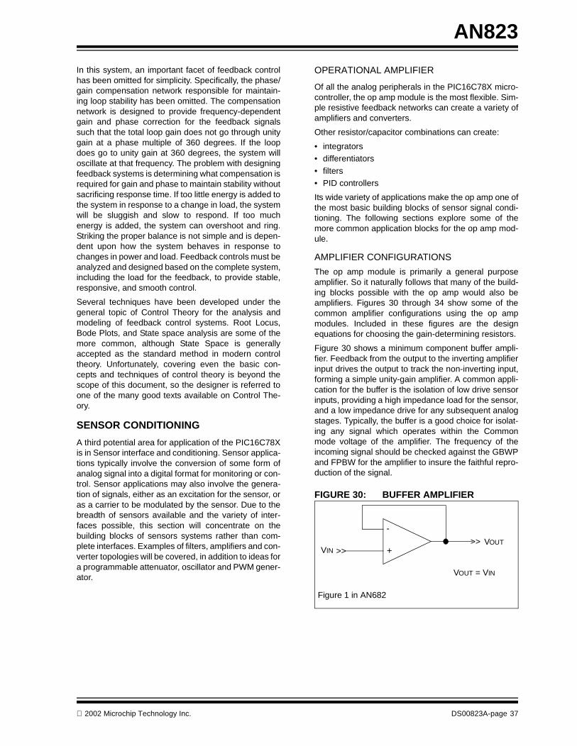
OPERATIONAL AMPLIFIER
One of the most versatile analog peripherals in thePIC16C78X is the Operational Amplifier module (OPA).The inverting and non-inverting pins are available onRA0 and RA1, with the amplifier output on RB3.Together, the three terminals comprise all the standardconnections for an operational amplifier (op amp).
DS00823A-page 10 2002 Microchip Technology Inc.
AN823
In addition to the three terminals of the device, addi-tional controls, available through the module’s periph-eral registers, allow the designer to:
• minimize the input offset voltage
• control the amplifier Gain Bandwidth Product• configure the amplifier as a voltage comparator
The following sections contain an overview of theamplifier's performance specifications and controloptions.
COMMON MODE VOLTAGE
The first parameters to be discussed concerning theperformance of the operational amplifier are the inputCommon mode voltage range and the output voltageswing. Common mode voltage is defined as the rangeof input voltages that the op amp can accept at itsinputs and still comply with its performance specifica-tions. For the op amp in the PIC16C78X, the Commonmode voltage is 0V to VDD-1.4V. For a 5VDC system,this would make the range 0V to 3.6V. While the rangeis somewhat restricted, it is important to note that boththe input and output Common mode voltages includeVSS (ground). Including ground in the Common moderange is particularly important for compatibility withground referenced sensors.
Like the Input Common Mode Voltage specification, theOutput Voltage Swing specification determines theminimum and maximum output voltages that can bedriven by the op amp. However, there are two importantnotes concerning this specification:
1. The output swing is affected by load, thereforethe Output Voltage Swing is always specifieddriving a specified load. Sourcing or sinkinghigher currents will reduce the output swing, andlower currents will increase the swing.
2. The linearity of the amplifier is not guaranteed tothe full Output Voltage Swing. Full Power Band-width should be used for determination of themaximum linear output swing for a given fre-quency signal.
The Common mode range also limits the input and out-put range of the op amp to positive voltages only. Whilemost amplifier configurations assume a differential sup-ply, modifications for single-ended supplies are not dif-ficult and a number of reference texts are availablewhich cover the required design techniques. Moreinformation concerning amplifier design from a singlesupply is available in the section covering sensoramplifier applications of the operational amplifier inApplication Note AN682.
GAIN BANDWIDTH PRODUCT
The next operational amplifier performance specifica-tion to be discussed is the Gain Bandwidth Product, orGBWP. All Voltage mode op amps are designed with alow pass filter function integrated into their design tostabilize their operation in feedback amplifier configura-tions. The low pass generally has a corner frequencybetween 0.1 and 200 Hz, and rolls off the gain of the opamp at a rate of 20 dB per decade of frequency. GBWPis defined as the frequency at which the internal lowpass function decreases the open loop gain of theamplifier to unity.
In design, the effect of GBWP is the loss of feedbackgain with frequency, resulting in a gradual increase inthe DC error of the output as the frequency of a signalincreases.
The op amp in the PIC16C78X family of microcontrol-lers has the option of two GBWP settings: 30 kHz (typ)or 3 MHz (typ). The reason for two GBWP settings isrelated to current consumption; the 30 kHz settingdraws less current than the standard 3 MHz setting.The 30 kHz setting is typically used in applications thathave a need for low power consumption at the expenseof speed. For example, slow speed sensors like tem-perature, humidity, or ion chambers in smoke detectorsoperating from battery power could use the 30 kHz set-ting. The 3 MHz GBWP setting is more common and istypically the choice for faster filter and control applica-tions.
SLEW RATE AND FULL POWER BANDWIDTH
Another important performance parameter is SlewRate, and its alternate representation, Full PowerBandwidth (FPBW). Slew rate is defined as the maxi-mum output voltage change over a specific time, typi-cally measured in V/µs. FPBW is another form of slewrate defined as the maximum frequency the output canbe driven over its full output range without distortion.FPBW and slew rate are related by Equation 2:
EQUATION 2: FULL POWER BAND BANDWIDTH AND SLEW RATE EQUATION
FPBW = Slew Rate
2π(VOMAX)*
*VOMAX = Maximum output voltage swingwithout significant distortion
2002 Microchip Technology Inc. DS00823A-page 11
AN823
In design, Slew Rate represents the limiting factor in anamplifier’s ability to track pulse and step functioninputs. FPBW translates slew rate into terms of fre-quency to define the ability of the amplifier to faithfullyreproduce the incoming sine wave over the output volt-age range. Both GBWP and FPBW are importantparameters to consider in the design of amplifier cir-cuits that are expected to operate near the high fre-quency limit of the operational amplifier.
Due to the GBWP setting control of the amplifier's gain,the GBWP setting will also affect Slew Rate and FPBWof the amplifier. Operating the amplifier with a GBWP of30 kHz will result in a corresponding reduction in theSlew Rate and FPBW of the amplifier. To determine theeffect upon the Slew Rate and FPBW due to the GBWPsetting, the designer is referred to the Specificationssection of the Data Sheet for graphs outlining the affectof GBWP setting on Slew Rate and FPBW.
INPUT OFFSET VOLTAGE
Input offset voltage is defined as a DC offset errorbetween the amplifier inputs. Typically, input offseterror is due to minor differences in the transistor pair atthe inputs to the amplifier. In older discrete op amps, apin was made available for connecting a trim resistorfor offset voltage adjustment. Newer microcontrollerapplications handle the problem by mathematically cal-ibrating out the offset. The drawback to manual adjust-ment is both the added cost of the manual operation/calibration as well as the dependence of input offsetvoltage upon ambient temperature. Additional calibra-tion time/cost of a single fixed adjustment calibration isof limited value.
The PIC16C78X has improved upon this process bymaking input offset voltage adjustment an automaticcalibration function under control of the software. Upondemand by the software, the automatic calibrationmodule will switch the op amp from its external connec-tions to an internal test circuit. The module then cali-brates the amplifier for minimum offset voltage whilebeing driven by a Common mode voltage reference.The calibration module offers the option of performingthe calibration with either a fixed 1.2V Common modevoltage, or with a programmable voltage supplied bythe DAC. In addition, the microcontroller can monitorthe ambient temperature using an external thermistorand, whenever a change in temperature is sufficientlylarge, recalibrate to minimize the offset voltage changewith temperature.
The calibration process is initiated by setting the CALbit in the CALCON register. If the process completesnormally, the CAL bit will be cleared to indicate a suc-cessful calibration. If a problem occurs with calibrationand it does not complete normally, the CALERR bit willset to indicate the error.
INPUT BIAS CURRENT / LEAKAGE CURRENT
The final parameter to discuss is the op amp’s low leak-age inputs, or as the specification is labeled in the DCCharacteristics chart, Input Bias Current. Much of theconfusion that exists over this specification is due to themisleading naming convention applied to these inputs,so a short explanation of the specifications and theirmeaning is in order. In discrete bipolar op amps, InputBias Current did indeed specify the current flowrequired to bias the input transistors of the amplifier. Indiscrete CMOS op amps, however, Input Bias Currentno longer specified a bias current since the input MOS-FET transistors do not have a gate bias current.Instead, the specification was re-used to specify theleakage currents associated with ESD and offset volt-age trim circuitry tied to the input pins. In thePIC16C78X op amp, the specification was widened toinclude the leakage currents of the other functions mul-tiplexed onto the pin as well. In all three cases, InputBias current specifies the current flow at the op ampinputs. The difference lies in the reason for the currentflow. That is why the PIC16C78X Data Sheet will referto the specification as both Input Bias Current, andInput Leakage Current. When discussing the perfor-mance of the op amp, Input Bias Current is used asstandard terminology for op amps. When discussingthe behavior of the pin in general, Leakage current isused for common terminology with other pin specifica-tions. In either case, the current flow specified for theamplifier inputs has been minimized as much as possi-ble in the design of the op amp.
Note: At lower frequencies, FPBW is limited bythe output swing of the amplifier. At higherfrequencies, FPBW is dictated by theamplifier slew rate (see Equation 2).
Note: Designers must remember that the perfor-mance of the op amp is only warrantedwhile the input Common mode voltagesare observed. Attempting to calibrate theop amp module outside the specified Com-mon mode voltage may result in calibrationfailure.
DS00823A-page 12 2002 Microchip Technology Inc.
AN823
In design, it is important to remember that, while thevalue of the current is small, (typically <50 nano-Amps),it can affect the performance of an amplifier that hasmismatched large input impedances. An amplifier withan effective input impedance of 100K ohm on one portand zero (0) ohms on the other can suffer over 5 mV ofoffset due to the voltage generated in the input/feed-back resistors in response to the input bias current.Large input impedances can also increase the noisevoltage of the amplifier. If a large input resistancenecessitates the use of large-valued resistors, theeffects of input bias current can be minimized by insur-ing that the Thevenin input impedance presented toboth the inverting and non-inverting inputs is equal.Driving the inputs with equal impedances generatesoffset voltages that are approximately equal and oppo-site, resulting in a cancellation at the output of theamplifier.
COMPARATOR MODE
One of the useful features of the op amp module is itsability to operate as a voltage comparator. Setting theCMPEN bit in the OPACON register converts the oper-ation amplifier into a voltage comparator. While thecomparator will not have a 4:1 multiplexer on its inputnor a multiplexed reference, all three terminals of thecomparator are available for use, just like the other twocomparators in the PIC16C78X. Also, due to the outputbeing multiplexed with port bit RB3, interrupt-on-change can be configured using the PORTB Interrupt-on-Change feature. In addition to interrupt, the othercontrols for the operational amplifier are also available.GBWP will change the response time of the compara-tor, similar to the speed control for comparators C1 andC2. The input offset calibration module is also availableto trim the input offset of the comparator, just as it trimsthe offset voltage in the operational Amplifier mode.
One advantage to the Op Amp/Comparator is the abil-ity to trim the comparator’s input offset voltage. To trimthe comparator’s input offset voltage, the module mustfirst be set into Amplifier mode for the calibration. Oncecalibration is complete, the module can be set back intoComparator mode and the comparator will retain theinput offset trim. In fact, performing a calibration on theoperation amplifier/comparator will yield a comparatorwith better input offset performance than the existingvoltage comparators C1 and C2.
OPERATIONAL AMPLIFIER TIPS
• Keep all Common mode input voltage between VSS and VDD-1.4V.
• Program all I/O pins corresponding to operation amplifier terminals for analog operation using the ANSEL register. Bits 0,1,7 = 1.
• Use 30 kHz GBWP setting for minimal power sup-ply current draw.
• For tight control of the input offset voltage, use an external Thermistor to measure ambient tempera-ture. When the temperature shift is sufficient to move the input offset voltage out of the needed tolerance, recalibrate input offset voltage to mini-mize it’s drift with temperature.
• Balancing the effective input impedance present at the inverting and non-inverting inputs can fur-ther minimize offset and noise voltages at the op amp output.
• To minimize input offset errors in Comparator mode, calibrate input offset voltage in operational Amplifier mode then switch to Comparator mode.
• To generate an interrupt using the Comparator mode of the operational amplifier, configure RB3 as a digital input and enable Interrupt-on-Change.
VOLTAGE COMPARATORS (C1 and C2)
The dual Voltage Comparator module is similar to thevoltage Comparators available in other Microchipmicrocontrollers. However, the module's response timehas been improved and the following new featureshave been added:
• Two response time options, normal and slow• Both comparators have the option of external out-
puts• Both comparators have output polarity control• Both comparators have independent Interrupt-on-
Change• Comparator C2 has the option to synchronize it's
output to the Timer1 clock• Both comparator outputs are mirrored to a com-
mon register for simultaneous reading• Each comparator incorporates an independent 4-
to-1 input multiplexers
COMMON MODE VOLTAGE
Similar to the operation amplifier, the voltage compara-tor input Common mode voltage range is limited to therange (VSS-0.7V) to (VDD-1.4). As with the op amp, theoperational specifications for the voltage comparatorsare only warranted for Common mode voltages withinthe specified voltage range. To monitor voltage greaterthan VDD-1.4, the signal must be scaled by a voltagedivider to shift the input voltage within the Commonmode voltage limits (See Figure 5).
In this example, VIN is scaled by the resistor divider R1,R2. The ratio of R1 and R2 is chosen to generate a volt-age within the Common mode range when VIN is at itsmaximum voltage.
2002 Microchip Technology Inc. DS00823A-page 13
AN823
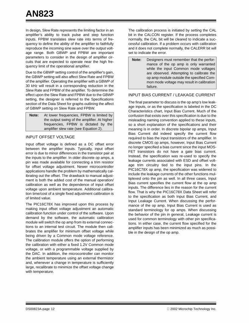
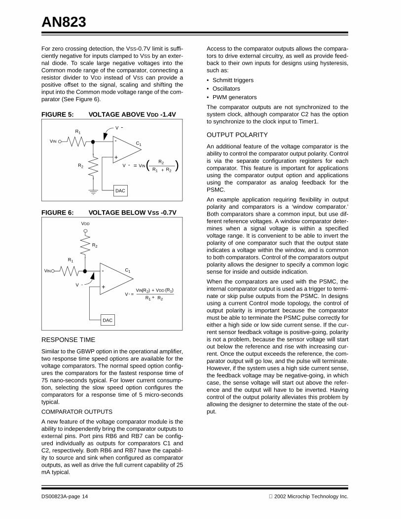
For zero crossing detection, the VSS-0.7V limit is suffi-ciently negative for inputs clamped to VSS by an exter-nal diode. To scale large negative voltages into theCommon mode range of the comparator, connecting aresistor divider to VDD instead of VSS can provide apositive offset to the signal, scaling and shifting theinput into the Common mode voltage range of the com-parator (See Figure 6).
FIGURE 5: VOLTAGE ABOVE VDD -1.4V
FIGURE 6: VOLTAGE BELOW VSS -0.7V
RESPONSE TIME
Similar to the GBWP option in the operational amplifier,two response time speed options are available for thevoltage comparators. The normal speed option config-ures the comparators for the fastest response time of75 nano-seconds typical. For lower current consump-tion, selecting the slow speed option configures thecomparators for a response time of 5 micro-secondstypical.
COMPARATOR OUTPUTS
A new feature of the voltage comparator module is theability to independently bring the comparator outputs toexternal pins. Port pins RB6 and RB7 can be config-ured individually as outputs for comparators C1 andC2, respectively. Both RB6 and RB7 have the capabil-ity to source and sink when configured as comparatoroutputs, as well as drive the full current capability of 25mA typical.
Access to the comparator outputs allows the compara-tors to drive external circuitry, as well as provide feed-back to their own inputs for designs using hysteresis,such as:
• Schmitt triggers• Oscillators
• PWM generators
The comparator outputs are not synchronized to thesystem clock, although comparator C2 has the optionto synchronize to the clock input to Timer1.
OUTPUT POLARITY
An additional feature of the voltage comparator is theability to control the comparator output polarity. Controlis via the separate configuration registers for eachcomparator. This feature is important for applicationsusing the comparator output option and applicationsusing the comparator as analog feedback for thePSMC.
An example application requiring flexibility in outputpolarity and comparators is a ‘window comparator.’Both comparators share a common input, but use dif-ferent reference voltages. A window comparator deter-mines when a signal voltage is within a specifiedvoltage range. It is convenient to be able to invert thepolarity of one comparator such that the output stateindicates a voltage within the window, and is commonto both comparators. Control of the comparators outputpolarity allows the designer to specify a common logicsense for inside and outside indication.
When the comparators are used with the PSMC, theinternal comparator output is used as a trigger to termi-nate or skip pulse outputs from the PSMC. In designsusing a current Control mode topology, the control ofoutput polarity is important because the comparatormust be able to terminate the PSMC pulse correctly foreither a high side or low side current sense. If the cur-rent sensor feedback voltage is positive-going, polarityis not a problem, because the sensor voltage will startout below the reference and rise with increasing cur-rent. Once the output exceeds the reference, the com-parator output will go low, and the pulse will terminate.However, if the system uses a high side current sense,the feedback voltage may be negative-going, in whichcase, the sense voltage will start out above the refer-ence and the output will have to be inverted. Havingcontrol of the output polarity alleviates this problem byallowing the designer to determine the state of the out-put.
+
-
R1
R2
VIN
DAC
VIN ( R1 + R2
R2 )
C1
V =-
V -
+
-
R1
R2
VIN
DAC
VIN
R1 + R2
(R2) + VDD
C1
V =-
VDD
V -(R1)
DS00823A-page 14 2002 Microchip Technology Inc.
AN823
TIMER1 CLOCK SYNCHRONIZATION
The new voltage comparator feature, unique to com-parator C2, is the ability to synchronize the output of thecomparator to the Timer1 clock. The output of compar-ator C2 is common to the same pin as the Timer1 gateenable input. The synchronization feature is designedto allow C2 to act as a control for the Timer1 gate inputwithout creating a race condition on the clock input.Timer1 is configured to always clock on the rising edgeof its clock signal. Synchronizing the output of C2 to thefalling edge of the clock ensures the gate signal willalways be stable prior to the active transition of theclock if C2 is used to generate the gate signal.
COMPARATOR TIPS
• To clear an Interrupt-on-Change generated by the comparator outputs, it is necessary to read the comparator output from the comparator configura-tion registers CM1CON0 or CM2CON0. Although both outputs are mirrored in CM2CON1, reading the CM2CON1 register will not clear the Interrupt-on-Change mismatch latch, which will regenerate the interrupt as soon as GIE is set.
• The bypass capacitor on the analog and digital VDD should be a 0.1 µF ceramic capacitor. If either capacitor is missing or ineffective, the com-parator output may oscillate when the comparator inputs are within 10 mV of each other due to feed-back through the power supply.
• An internal connection between the DAC and the comparator allows the designer to create a pro-grammable threshold comparator without an external connection to either reference. In addi-tion, the DAC reference can be programmed for the VREF1 input, allowing the software to scale an external reference input to the comparators.
• The output bits present in the CM1CON0, CM2CON0, and CM2CON1 registers are syn-chronized to the internal microcontroller clock. The external outputs of the voltage comparators are asynchronous to the microcontroller clock.
VOLTAGE REFERENCE (VR)
Another useful module in the PIC16C78X microcontrol-ler is the on-board voltage reference. The VR moduleprovides a stable 3.072V reference voltage, and mostof the analog modules within the PIC16C78X micro-controller have the option to use the VR module as theirinternal voltage reference. In addition, the VR modulehas the option to provide an output for external circuitryon pin RB0.
BANDGAP REFERENCE
The internal reference standard for the VR module is astable bandgap reference circuit, which is enabledwhenever the VR module, Brown-out Reset (BOR) cir-cuit, or Programmable Low Voltage Detect (PLVD)module is selected. In all three cases, the bandgap ref-erence will remain active so long as the module usingthe reference is enabled.
During the initial stabilization time following startup, theBandgap reference may not be compliant with its spec-ifications for accuracy and drift. To assist with the con-trol of circuits that may use the reference, a stability flagBGST in the LVDCON register is provided to indicatewhen the reference has stabilized to within its specifiedperformance level. Systems that rely on the stability ofthe reference voltage should monitor this flag and delayany critical measurements until after the flag is set, indi-cating the Bandgap reference has stabilized.
The electrical parameters that are important for anydesign utilizing the internal reference are:
• Bandgap startup time• Temperature coefficient• Load regulation
• Supply regulation
Bandgap startup time is defined as the warm-up timedelay between enabling the Bandgap reference andthe time when the reference has stabilized to within itsspecified accuracy. Temperature coefficient specifiesthe output voltage drift of the reference with changes inthe ambient temperature. Load regulation specifies theoutput voltage shift in response to changes in the loadpresent on the RB0 pin. And finally, supply regulationspecifies output voltage shift with changes in the supplyvoltage.
BANDGAP STARTUP TIME
The time required for the Bandgap reference to stabi-lize is specified in the Data Sheet to be no more than30 µs. However, determining the start of the stabiliza-tion time can be ambiguous due to the number of mod-ules that can enable the VR module. The BOR, PLVDand VR modules can all enable the reference and, tocomplicate the issue, the BOR circuit is enabledthrough the configuration fuses (not software) so themodule may already be enabled when the devicecomes out of RESET. To assist in determining the sta-bility of the reference, a BGST flag has been includedin the PLVD configuration register. This bit will becleared until the Bandgap has stabilized, after whichthe bit will be set indicating that the reference has beenenabled and has stabilized. It is recommended that anytime the VR module is enabled, all peripherals refrainfrom using the VR module as a reference until theBGST bit is set.
2002 Microchip Technology Inc. DS00823A-page 15
AN823
OUTPUT VOLTAGE TEMPERATURE COEFFICIENT
The Output Voltage Temperature Coefficient is notspecified for the Bandgap reference directly. Instead,the temperature coefficient is specified for the band-gap/VR module combination. This parameter is speci-fied in parts per million per degree Centigrade (ppm/C).To determine the actual voltage change with tempera-ture, Equation 3 can be used.
EQUATION 3: VOLTAGE CHANGE WITH TEMPERATURE
LOAD REGULATION
Load regulation is defined as the change in output volt-age per milli-amp of current sourced by the VR moduleoutput. In practice, this means that the output voltageof the VR module will sag with load current. Typicallythe parameter is specified as milli-volts/milli-amp. Todetermine the specific output voltage for a specific loadresistance on RB0, use equation 4:
EQUATION 4: LOAD RESISTANCE EQUATION
From Equation 4, it can be seen that the lower the loadresistance on the RB0/VR pin, the greater the shift inthe reference voltage output. Therefore, for high cur-rent loads, it is recommended that the RB0/VR outputbe buffered to prevent inaccuracies in the output volt-age.
SUPPLY REGULATION
Supply regulation specifies the change in output volt-age with changes in the microcontroller supply voltage.This parameter is specified in milli-volts/volt, sochanges in power supply voltage on the order of voltswill only have milli-volts of effect on the reference out-put. Typically, this value is 1 mV/V giving an output shiftof less than 0.1% over the entire power supply range ofthe part (2.7V to 5.5V). For applications using 8-bitADCs and DACs, this is less than ¼ of 1 LSb.
VOLTAGE REFERENCE TIPS
• The minimum resistive load that should be con-nected to the VR output without violating the load and current specifications of the module is 680 ohms.
• Using a resistive divider between the VR output and VSS is a simple, inexpensive method for gen-erating a virtual ground for single ended op amp circuits.
• When using a resistive divider to generate a vir-tual ground, the parallel combination of the resis-tor values should equal the Thevenin equivalent of the input and feedback resistances in the amplifier circuit.
• The internal and external VR module outputs that are isolated by a buffer amplifier internal to the part, so using the reference internally does not affect the output load regulation of the module.
DIGITAL-TO-ANALOG CONVERTER
A new peripheral in the PIC16C78X microcontrollers isthe 8-bit Digital-to-Analog converter, or DAC. The DACis a Voltage mode converter capable of a rail-to-rail out-put. Specifications for the DAC include parametersdescribing:
• Linearity
• Output drive capability• Response to external signals input into the mod-
ule’s reference input
Configuration options include an external output on theRB1/VDAC pin and reference voltage selection. Formore information concerning programming of the DAC,please refer to the chapter covering the DAC in thePIC16C78X Data Sheet (DS41171). Available atwww.microchip.com.
SLEW RATE AND SETTLING TIME
Two of the important parameters for the DAC are itsoutput Slew Rate and settling time. Because the DACcan utilize an external voltage reference through theVREF1 input, it has applications in scaling external sig-nals for conversion in the ADC or level sensing usingthe voltage comparators. As a result, the ability of theDAC to accurately track an external signal is importantto the overall accuracy of the ADC or comparator cir-cuitry. Slew Rate specifies how fast the output canchange voltage in response to a reference change, ora change in the DAC binary value, and is similar to theop amp slew rate specification. Settling time specifiesthe time for an output to settle the within ½ LSb of itsfinal value. Together, they specify how long it takes theDAC output to transition from one voltage to another inresponse to a change.
∆VOUT =(TEMP COEFF)*(∆T)*(3.072V)
106
VOUT[mV] = Load Reg*(3.072V)(1000)
RLOAD (OHMS)
DS00823A-page 16 2002 Microchip Technology Inc.
AN823
ACCURACY/LINEARITY
The accuracy/error specified for the DAC moduleincludes:
1. Integral non-linearity error (INL)2. Differential non-linearity error (DNL)3. Gain error
4. Offset error5. Monotonicity
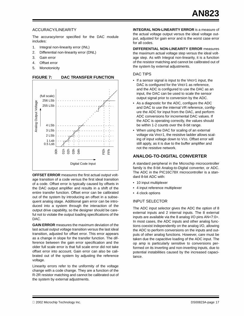
FIGURE 7: DAC TRANSFER FUNCTION
OFFSET ERROR measures the first actual output volt-age transition of a code versus the first ideal transitionof a code. Offset error is typically caused by offsets inthe DAC output amplifier and results in a shift of theentire transfer function. Offset error can be calibratedout of the system by introducing an offset in a subse-quent analog stage. Additional gain error can be intro-duced into a system through the interaction of theoutput drive capability, so the designer should be care-ful not to violate the output loading specifications of theDAC.
GAIN ERROR measures the maximum deviation of thelast actual output voltage transition versus the last idealtransition, adjusted for offset error. This error appearsas a change in slope for the transfer function. The dif-ference between the gain error specification and theolder full scale error is that full scale error did not takeoffset error into account. Gain error can also be cali-brated out of the system by adjusting the referencevoltage.
Linearity errors refer to the uniformity of the voltagechange with a code change. They are a function of theR-2R resistor matching and cannot be calibrated out ofthe system by external adjustments.
INTEGRAL NON-LINEARITY ERROR is a measure ofthe actual voltage output versus the ideal voltage out-put, adjusted for gain error and is the worst case errorfor all codes.
DIFFERENTIAL NON-LINEARITY ERROR measuresthe maximum actual voltage step versus the ideal volt-age step. As with Integral non-linearity, it is a functionof the resistor matching and cannot be calibrated out ofthe system by external adjustments.
DAC TIPS
• If a sensor signal is input to the VREF1 input, the DAC is configured for the VREF1 as reference, and the ADC is configured to use the DAC as an input, the DAC can be used to scale the sensor output signal prior to conversion by the ADC.
• As a diagnostic for the ADC, configure the ADC and DAC to use the internal VR reference, config-ure the ADC for input from the DAC, and perform ADC conversions for incremental DAC values. If the ADC is operating correctly, the values should be within 1-2 counts over the 8-bit range.
• When using the DAC for scaling of an external voltage via VREF1, the resistive ladder allows scal-ing of input voltage down to VSS. Offset error will still apply, as it is due to the buffer amplifier and not the resistive network.
ANALOG-TO-DIGITAL CONVERTER
A standard peripheral in the Microchip microcontrollerfamily is the 8-bit Analog-to-Digital converter, or ADC.The ADC in the PIC16C78X microcontroller is a stan-dard 8-bit ADC with:
The ADC input selector gives the ADC the option of 8external inputs and 2 internal inputs. The 8 externalinputs are available via the 8 analog I/O pins AN<7:0>.In most cases, the ADC inputs and other analog func-tions coexist independently on the analog I/O, allowingthe ADC to perform conversions on the inputs and out-puts of other analog functions. However, care must betaken due the capacitive loading of the ADC input. Theop amp is particularly sensitive to conversions per-formed on its inverting and non-inverting inputs, due topotential instabilities caused by the increased capaci-tance.
Ana
log
Out
put V
olta
ge
256 LSb
255 LSb
4 LSb
3 LSb
2 LSb
1 Lsb
00h
01h
02h
03h
04h
FE
h
FF
h
Digital Code Input
0.5 Lsb
(full scale)
2002 Microchip Technology Inc. DS00823A-page 17
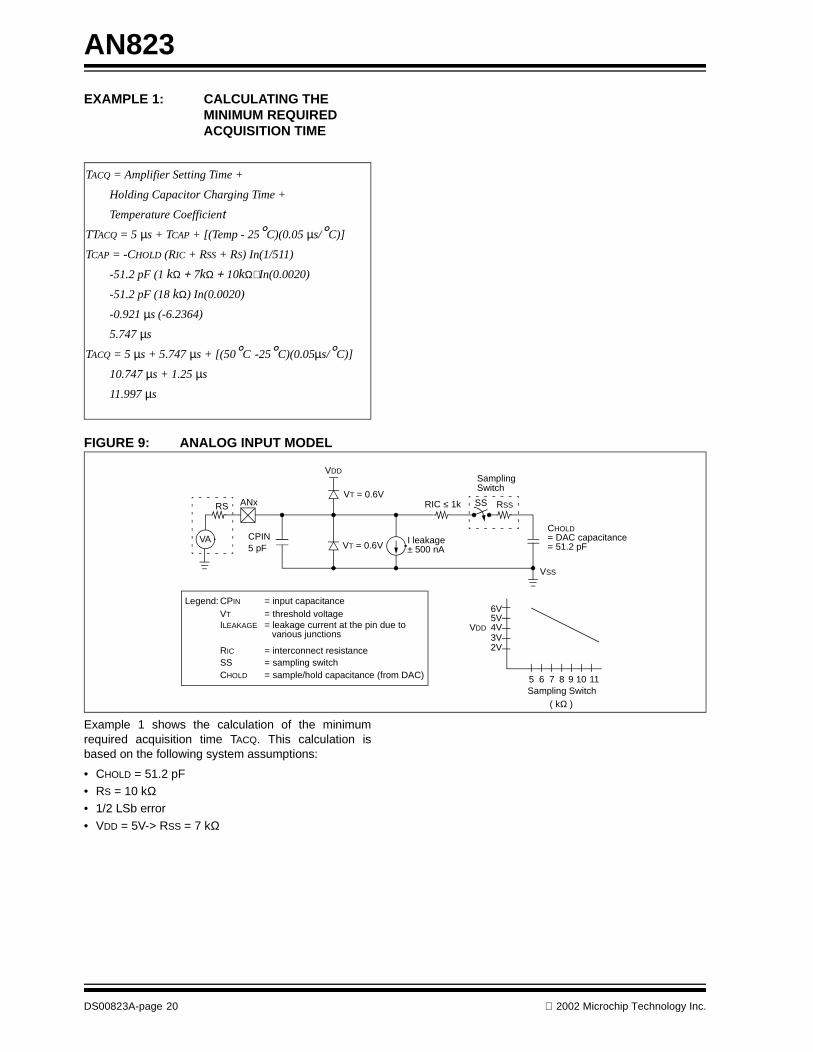
AN823
The two additional internal inputs are connected to theDAC and VR signals internally for both diagnostic andcompound functions. The internal connection of thesetwo signals allows an internal verification of the ADCperformance as a simple diagnostic. Using the DAC,the ADC can completely verify its operation by perform-ing successive conversions on the DAC output as theDAC is stepped from 00h to FFh, validating all codeswithout requiring an external connection. Using theinternal DAC input, a compound function can also becreated using the DAC as a voltage scaling input for theADC. This configuration allows the software to scale asensor input for the greatest possible conversion reso-lution.
ANALOG I/O SELECTION
An important point to remember is that any pin used asan analog input should be configured for analog use viathe ANSEL register. When analog voltages are presenton the input to a digital input buffer, both the N and Pchannel devices in the buffer are driven into their linearregion, causing partial conduction in both devices.When both devices conduct, an additional supply cur-rent is passed from VDD to VSS, increasing the currentdraw of the device. Therefore, it is recommended thatany pin with a linear voltage present be configured foranalog operation by setting (=1) the corresponding bitin the ANSEL register.
REFERENCE SELECTOR
The four reference voltage options available with ADCinclude the:
• Internal VR voltage reference• AVDD power supply voltage• DAC output voltage
• External reference input VREF1
The internal VR voltage reference supplies a costeffective, Bandgap stabilized, 3.072 voltage reference.AVDD as a reference give the ADC it's maximum possi-ble input range. The output of the DAC allows thedesigner to scale the ADC reference for the maximumresolution for each individual input. And finally, to allowfor custom reference voltage, the ADC has the optionto use an external reference input on VREF1.
CLOCK OPTIONS
The ADC module has the option of 4 separate clockingoptions: three divided from the microcontroller clock,and one from an internal RC oscillator. The clockoptions allow the generation of the following conversiontimes, as shown in Table 2.
Legend: Shaded blocks are outside recommended range1: The RC source has a typical conversion time of 38 µs.2: These values violate the minimum required Tad time.3: For faster conversion times, the selection of another clock source is recommended.4: When device frequency is greater than 1 MHz, the RC ADC conversion clock source is recommended for
SLEEP operation only.
TABLE 2: CONVERSION TIME VS. MICROCONTROLLER CLOCK
The absolute accuracy (absolute error) specified for theADC includes the sum of all contributions for:
• Offset error• Gain error• Quantization error
• Integral non-linearity error• Differential non-linearity error• Monotonicity
FIGURE 8: ADC TRANSFER FUNCTION
The absolute error is defined as the maximum devia-tion from an actual transition versus an ideal transitionfor any code. The absolute error of the ADC is specifiedas < ± 1 LSb for ADCREF = VDD (over the device'sspecified operating range) (see Figure 8). However, theaccuracy of the ADC degrades as VDD diverges fromADCREF.
For a given range of analog inputs, the output digitalcode will be the same. This is due to the quantization ofthe analog input to a digital code. Quantization erroris typically ± ½ LSb and is inherent in the analog-to-dig-ital conversion process. The only way to reduce quan-tization error is to use an ADC with a greater resolution.
Offset error measures the first actual transition of acode versus the first ideal transition of a code. Offseterror shifts the entire transfer function and is due to off-set error in the amplifiers of the ADC. Offset error canbe calibrated out of a system through the induction ofoffsets in the preceding analog functions. Additional off-set errors can be introduced into the system throughthe interaction of the input leakage current and sourceimpedance at the analog input, so care should be takenin the design of the input circuitry.
Gain error measures the maximum deviation of thelast actual transition and the last ideal transitionadjusted for offset error. This error appears as achange in the slope of the transfer function. The differ-ence between gain error and full scale error is that fullscale error does not take offset error into account. Gainerror can usually be calibrated out in software.
Linearity error refers to the uniformity of the codechanges. The problem with linearity errors is the inabil-ity to calibrate them out of a system. Integral Non-Lin-earity error is a measure of the actual code transitionversus the ideal code transition, adjusted by the gainerror for each code. Differential Non-Linearity mea-sures the maximum actual code width versus the idealcode width. This measure is not adjusted.
If the linearity errors are very large, the ADC maybecome Non-Monotonic. This occurs when the digitalvalues for one or more input voltages are less than thevalue for the next lower input voltage step.
ACQUISITION TIME AND CONVERSION SPEED
For the ADC module to meet its specified accuracy, theinternal Sample-and-Hold capacitor (CHOLD) must beallowed to charge to within ½ LSb of the voltagepresent on the input channel (see Analog Input Modelin Figure 8). The analog source resistance (RS) and theinternal sampling switch resistance (RSS) will directlyaffect the time required to charge CHOLD. In addition,RSS will vary over the power supply voltage range(AVDD), and RS will affect the input offset voltage at theanalog input (due to pin leakage current). Therefore:
1. The maximum recommended impedance forany analog sources is 10 kOhms.
2. Following any change in the analog input chan-nel selection, a minimum acquisition delay mustbe observed before another conversion canbegin.
To calculate the minimum acquisition time, Equation 5may be used. This equation calculates the acquisitiontime to within ½ LSb error, assuming an 8-bit conver-sion (512 steps for the PIC16C781/782 ADC). The ½LSb error is the maximum error allowed for the ADC tomeet its specified accuracy (see Example 1).
• Care must be taken when using the AN6 pin in ADC conversions due to its close proximity to the OSC1 pin if the external oscillator is enabled.
• For current and noise reduction, the ADC can be configured to operate while the microcontroller is in SLEEP mode. The clock source for the ADC must be the ADC RC oscillator, because the microcontroller clock will be stopped during SLEEP.
• Acquisition time is affected by the impedance of the source driving the ADC input. Designers should review the previous section to insure suffi-cient acquisition time following the selection of a new analog channel.
• The ADC input uses a capacitive sample and hold on it's input channel as part of the conversion pro-cess. Care must be taken not to initiate a conver-sion on either the inverting or non-inverting channel of the op amp, as the added capacitance can cause instability in the feedback of the ampli-fier.
PROGRAMMABLE SWITCH MODE CONTROLLER
A new mixed signal peripheral in the PIC16C78X is the Programmable Switch Mode controller or PSMC. The primary purpose of the PSMC is to control the drive of external power systems using Pulse mode control. It can operate as either a Pulse Skipping Mod-ulation or Pulse Width Modulation control. Its mixed signal nature is due to its ability to regulate the pres-ence and/or width of the pulses in response to analog feedback via the comparator module.
There are several advantages to Pulse mode control:
1. Pulse mode control systems are very linear. Thelinearity of a Pulse mode system is dictated bythe accuracy of the pulse timing rather than indi-vidual drive transistor linearity.
2. Pulse mode control systems are more powerefficient. The power drive circuitry of Pulsemode systems operate in the saturation regionof the transistors resulting in the absolute mini-mum power dissipation for the devices. The min-imal loss in Pulse mode driver makes the Pulsemode control system one of the most efficientpower control and transfer system topologies.Linear systems, on the other hand, operate theirdrivers in the linear region of the transistors,resulting in a much higher power dissipationand, as a result, a much lower efficiency.
3. Pulse mode power control systems can gener-ate output voltages greater than, less than, andwith the same or opposite polarity relative totheir supply. Linear power control systems canonly generate output voltages less than (and thesame polarity as) their supply.
With the higher efficiency of Pulse mode controls andtheir reliance on timing rather than linear operation, thePSMC is an obvious control peripheral choice for anymicrocontroller-based power system.
PULSE MODE
The PSMC can generate either a Pulse Width Modu-lated (PWM) or Pulse Skip Modulated (PSM) output.Pulse Width Modulation varies the width of the outputpulse based on analog feedback from the comparators.Pulse Skip Modulation controls the presence orabsence of fixed width pulses based on feedback fromthe comparators (See Figure 10 and 12).
PWM
To configure the PSMC for PWM mode, three valuesmust be set:
1. Pulse frequency2. Minimum duty cycle3. Maximum duty cycle
The pulse frequency is a function of the microcontrol-lers clock frequency and the prescaler selection inthe PSMC. Equation 6 is used to determine the pulsefrequency.
Note 1: The reference voltage (ADCREF) has noeffect on the equation, since it cancelsitself out.
2: The charge holding capacitor (CHOLD) isnot discharged after each conversion.
3: The maximum recommended impedancefor analog sources is 10kΩ. This isrequired to meet the pin leakage specifi-cation.
2002 Microchip Technology Inc. DS00823A-page 21
AN823
EQUATION 6: PULSE FREQUENCY EQUATION
Equation 6 can also be reversed to give microcontrollerfrequencies options for a desired pulse frequency usingEquation 7:
EQUATION 7: DESIRED PULSE FREQUENCY
Using the prescaler and various oscillator frequenciesfor the microcontroller, pulse frequencies as low as 289Hz can be generated using the internal 37 kHz oscilla-tor, or as high as 1.25 MHz can be generated from a 20MHz crystal.
The minimum and maximum duty cycle settings areapplication-specific and cannot be determined by a uni-versal equation. The designer is therefore referred tothe appropriate reference documentation for the type ofdesign and topology to be used. The PSMC is capableof the following minimum and maximum duty cycle set-tings shown in Tables 2 and 3.
PULSE SKIP MODE (PSM)
To configure the PSMC for PWM mode, two valuesmust be set:
1. Pulse frequency2. Duty cycle
The pulse frequency is a function of the microcontrol-lers clock frequency and the prescaler selection in thePSMC. The equations outlined in the previous sectionsare the same for both PSM and PWM operation.
The duty cycle setting is a function of the drive topol-ogy, and as in the previous section, cannot be deter-mined by a universal equation. The appropriatereference documentation for the type of design andtopology are listed at the end of this Application Note.The PSMC is capable of the following fixed duty cyclesettings shown in Table 4:
SINGLE/DUAL FEEDBACK
To support a wide variety of topologies, the PSMC hasthe option to use either single or dual feedback from thecomparator module. In single channel feedback, onlycomparator C1 is used as an input by the PSMC. Thelogic sense of the feed back is negative true, (i.e., if theoutput of the comparator goes low, then PSMC pulsesare either terminated or skipped, depending upon themodulation used). In dual channel feedback, compara-tors C1 and C2 are used as sources of feedback by thePSMC. The logic sense for dual channel feedback isnegative true OR, (i.e., if the output of comparator C1OR C2 goes low, then PSMC pulses are either termi-nated or skipped, depending upon the modulationused).
SINGLE/DUAL OUTPUT
The PSMC also has the option of a Single or a Dual(alternating) output. In single Output mode, the PSMCgenerates pulses at the rated specified by the micro-controller oscillator and the prescaler selection on thePSMC1A output only. In the Single mode, pin RB7 isalso available as a general purpose I/O.
In dual Output mode, pulses are generated alternately:first on pin RB7, then on RB6, then again on RB7 andso on. Each output produces pulses at ½ the calculatedrate, with the combination of RB6 and RB7 generatingthe full frequency of pulse (see Figures 10, 11, and 12).
TABLE 2: MINIMUM DUTY CYCLE
Minimum Duty Cycle MINDC<1:0>
0.0% 00
12.5% 01
25.0% 10
37.5% 11
TABLE 3: MAXIMUM DUTY CYCLE
Maximum Duty Cycle MAXDC<1:0>
50.00% 00
62.5% 01
75.0% 10
93.75% 11
FPULSE = Fosc
16* prescaler
FOSC = FPULSE*16*PS
FOSC is calculated for PS = 1, 2, 4, and 8
TABLE 4: FIXED DUTY CYCLE SETTINGS
Fixed Duty Cycle DC<1:0>
12.50% 00
37.50% 01
62.50% 10
93.75% 11
DS00823A-page 22 2002 Microchip Technology Inc.
AN823
FIGURE 10: PSMC MODULE IN SINGLE OUTPUT PWM MODE
FIGURE 11: PSMC MODULE IN DUAL ALTERNATING OUTPUT PWM MODE
FIGURE 12: PSMC MODULE IN SINGLE OUTPUT PSM MODE
An additional output feature of the PSMC is the abilityto control the polarity of each output individually.Whether operating in single or dual Output modes, thepolarity of each output can be configured as either pos-itive active or negative active. This feature alleviatesthe need for combination inverting and non-invertingMOSFET drivers. With individual polarity control, thesoftware can configure the drive appropriately for eitherdrive sense, or even opposite drive sense for each out-put. In fact, in some cases the output drive of RB6 andRB7 may be sufficient for direct drive of MOSFET tran-sistors, in which case the ability to configure outputpolarity is a necessity.
SLOPE COMPENSATION OUTPUT
A final feature of the PSMC is the optional slope com-pensation output. The slope compensation output is anopen drain drive which pulls the output low for the last1/16th of every cycle. Its purpose is to generate apseudo-ramp wave form which is used for slope com-pensation (see Figure 13).
Slope compensation is a feature in switching powersupplies which helps maintain stability when the outputduty cycle exceeds 50%. When a switching power sup-ply exceeds 50% duty cycle, it becomes susceptible toimpulse noise from its supply side power source. Theimpulse noise can cause an exponentially increasingoscillation in the control loop that eventually leads tocatastrophic failure. Slope compensation prevents thisoccurrence by generating a ramp function that is com-bined with the feedback, resulting in a reduction in thefeedback level. The reduced feedback acts as adamper on the oscillation, quieting the response andrestoring stability. For more information concerninghow to implement slope compensation, please refer tothe power supply design reference at the end of thisApplication Note.
The ramp waveform generated by the slope compen-sation output has another use. In Voltage mode powersupplies, a ramp waveform is compared to a feedbackerror voltage. When the ramp voltage exceeds the errorvoltage, the output pulse is terminated and the inductordischarges into the output capacitor. For this mode towork, a ramp function is required that is synchronizedto the pulse generator. The required ramp can be gen-erated by the slope compensation output.
PSMC TIPS
• Whenever the PSMC is enabled in dual Output mode, the first pulse is always generated on the RB7 pin, then the RB6 pin.
• An important point to remember is that the TRISB register must be configured for RB6 and RB7 to be outputs if they are to operate as the pulse out-puts of the PSMC. If bits 6 and 7 of TRISB are set, the pins will be configured as inputs and no pulse will be generated.
• If the PSMC is disabled, the outputs on RB6 and RB7 will return to the configuration of the next highest priority (comparator or digital output). Designers are cautioned to read Chapter 3 of the Data Sheet carefully concerning precedence of control for I/O port pins.
• During RESET, the outputs of the PSMC will be configured as inputs. It is important that any driver designs using RB6 and/or RB7 must default to an inactive state during RESET to prevent damage to the driver circuitry.
• One method of gating the pulse output of the PSMC in PWM mode is to program a minimum duty cycle of 0% and enable dual channel input, but enable only comparator C1. The polarity con-trol of C2 will now operate as a software control, gating the output pulses on and off based on the state of the polarity bit.
• To improve the linearity of the ramp function gen-erated by the slope compensation output, replace the pull-up resistor with a constant current source (See the Applications section concerning Op Amp designs).
ENHANCED TIMER 1
A modified original peripheral in the PIC16C78X is theenhanced Timer1 module. Timer1 operates in muchthe same way as it does in other microcontrollers, butwith a few differences:
1. Timer1 does not have a separate oscillator.Instead, it can be configured to use the micro-controllers LP oscillator.
PWM Signalon PSMC1A
SC Switchon PSMC1B
Voltage across C
t = 0 t = 15/16T
DC = duty cycle
T = Period
- On
- Off
R
C
VDDPSMC1A
PSMC1B
To SlopeCompensationCircuit
SC Switch
PSMCModule
VSS
PIC16C78X
pin
pin
150
VDD
VSS
DS00823A-page 24 2002 Microchip Technology Inc.
AN823
2. The Timer1 clock input has been moved to RA6and is only available with Oscillator modes thatdo not use this pin (EC mode, INTRC w/o CLK-OUT, or RC w/o CLKOUT).
3. A clock gate input has been added to pin RB7which enables/disabled the clock input to thecounter, following the prescaler. When the gat-ing function is enabled, and the T1G is high, thecounter is stopped. When the input is pulled low,the counter resumes counting.
TIMER1 OSCILLATOR
To minimize the number of functions multiplexed ontothe microcontroller I/O pins, the normal Timer1 oscilla-tor circuit has been replaced with a connection to theLP microcontroller oscillator. The LP oscillator has thesame frequency capability as the original Timer1 oscil-lator, and like the Timer1 oscillator, the LP oscillator willcontinue to operate while the microcontroller is inSLEEP mode. In fact, when the LP oscillator is enabledvia the Timer1 OSCEN bit, the oscillator will continue torun even if the timer itself is disabled. So oscillator star-tup time is not a factor in the timer accuracy.
TIMER1 CLOCK INPUT
The Timer1 external clock input has been multiplexedwith the microcontroller I/O pin RA6. Among other func-tions, RA6 is also multiplexed with the microcontrollerOSC2 and CLKOUT functions. Therefore, the T1CKIfunction is only available when the microcontroller isoperating in one of three Oscillator modes:
• EC - external clock input• INTRC w/o CLKOUT
• RC w/o CLKOUT
With the exception of the limit on availability, the T1CKIinput is identical to the standard T1CKI input and iscapable of operating to the full speed of the timer.
TIMER1 GATE ENABLE
Timer1 has been enhanced with a new optional clockenable feature T1G. T1G is an active low input, whichwhen enabled, allows an external signal to gate theclock input to Timer1. The gate is located just beforethe Timer1 prescaler clock input. An active low on theinput enables the prescaler and counter to incrementon the rise edge of each clock. A high level input dis-ables the Timer1 count and holds the prescaler/counterat their current values.
TIMER1 TIPS
• For proper operation, the T1G should be synchro-nized to the falling edge of the Timer1 clock.
• The T1G input can be used to measure the PSMC PWM output in switching power supply applica-tions. The pulse width is proportional to the cur-rent supplied to the switching power supply output.
Note: To use the LP oscillator, the microcontrol-ler must be using the INTRC Oscillatormode, without CLKOUT
Note: When the LP Oscillator mode is enabled asa clock for the microcontroller, the oscilla-tor halts oscillation during SLEEP mode.
Note: Operating the T1CKI input at speedsgreater than the clock frequency of themicrocontroller is not recommended due totimer synchronization problems. Pleaserefer to the PIC16C78X Data Sheet formore information concerning this limita-tion.
2002 Microchip Technology Inc. DS00823A-page 25
AN823
APPLICATIONS
The final section of this Application Note deals withapplications for the individual/multiple peripherals byfunction. The purpose of this section is to provide thedesigner with possible application examples, not an in-depth tutorial in the design of a particular application.Further, the designs have been simplified to the mini-mum configuration to demonstrate the application.Where possible, references for further information areprovided for supplemental design information.
SWITCHING POWER CONVERSION
The first potential area for applications of thePIC16C78X microcontroller is Switch mode power sup-plies. Switch mode power supplies or ‘Switchers’ arebased on the concept of transferring energy in aswitched inductive or capacitive element. The Switchercycle begins by charging the transfer element, typicallyan inductor, with current. Next, the transfer element isswitched to the load where the current charge flowsinto an output hold capacitor. The load then draws cur-rent from the output capacitor during the next chargingcycle. The feedback loop is closed when the outputvoltage is compared against a reference, and theamount of charge in the next cycle is adjusted to com-pensate for any difference between the desired andactual output voltage.
Before diving into an explanation of the various switch-ing power supply topologies, three basic conceptsshould be covered:
1. Voltage mode versus current mode control2. Continuous versus discontinuous current opera-
tion3. Proportional versus hysteresis feedback
All three concepts are common to almost all Switchertopologies, and a short explanation of each is useful inthe discussion of the various switcher topologies.
VOLTAGE MODE
In Voltage mode control, a ramp waveform is used incombination with a feedback error signal to generate aPWM pulse. The PWM pulse is synchronized to theramp waveform and goes active with the start of theramp. The pulse stays active until the ramp voltageexceeds the feedback error signal, terminating the out-put pulse. The result is a pulse width proportional to themagnitude of the error signal voltage.
Figure 14 shows a block diagram of how a Voltagemode, proportional feedback controller can be imple-mented with the PSMC. The Slope Compensation out-put has an RC network attached to generate a pseudoramp waveform at the input to the voltage comparator.The other input to the comparator is driven by an erroramplifier which supplies an error voltage proportional tothe difference between the desired voltage and theactual output voltage. At the start of the cycle, thePSMC initiates an output pulse. The ramping voltagefrom the slope compensation network continues until itexceeds the error voltage from the difference amplifier.When the ramp exceeds the error voltage, the PSMCends the pulse and waits for the last 1/16th of the cycle.During the 1/16th of the cycle, the PSMC grounds theslope compensation output, which zeros the ramp forthe next cycle and the pulse sequence starts over.
DS00823A-page 26 2002 Microchip Technology Inc.
AN823
FIGURE 14: VOLTAGE MODE PROPORTIONAL FEEDBACK (PWM MODE ONLY)
FIGURE 15: VOLTAGE MODE HYSTERESIS FEEDBACK (PSM MODE ONLY)
Figure 15 shows a block diagram of how a Voltagemode, hysteresis feedback controller can be imple-mented with the PSMC. The PSMC is set up to gener-ate a fixed pulse output at the start of each cycle. Justprior to the initiation of the pulse, the PSMC tests thecomparator feedback to determine if a pulse isrequired. If the feedback voltage is greater than the ref-erence, no pulse is generated. If, however, the feed-
back voltage is lower than the reference, the PSMCgenerates the fixed pulse width until the feedback volt-age is back above the reference.
Due to the simplicity of Voltage mode operation, topol-ogies using Voltage mode control typically have fewercomponents and are somewhat easier to design. How-ever, one of the main draw backs to Voltage mode isthat it does not monitor the current flow in the inductor,which can result in a ‘ratcheting up’ of the magnetic
FOSC
PSMC
PSMC1APRESCALER
+
-
VREF
+
-
PULSE OUTPUT TO
C1
(CURRENT FEEDBACK NOT USED)
VOLTAGEFEEDBACK
OPA
SC
RSC
VDD
CSC
V
TIME
SC WAVEFORM
POWER SWITCH
Peripherals internal to PIC16C781/782
FOSC
PSMC
PSMC1APRESCALER
+
VREF
+
-C1 VOLTAGEFEEDBACK
SC
(CURRENT FEEDBACK NOT USED)
PULSE OUTPUT TOPOWER SWITCH
Peripherals internal to PIC16C781/782
2002 Microchip Technology Inc. DS00823A-page 27
AN823
field in the inductor until the core saturates. When aninductor core saturates, its inductance drops, chargecurrent significantly increases and the result is usuallythe spectacular failure of the MOSFET switching tran-sistors.
CURRENT MODE
In Current mode control, a second inner control loopgenerates the PWM pulse width based on the errorvoltage and the current flow in the MOSFET/inductor.At the start of the cycle, a pulse is asserted by thePSMC. The current in the MOSFET/inductor is moni-tored, resulting in a ramp voltage proportional to theinstantaneous current flowing in the pair. When theramp voltage exceeds the error signal, the PSMC ter-
minates the pulse. When the MOSFET turns off, thecurrent flow in the inductor finds an alternate paththrough the diode, resulting in the charging of the out-put capacitor.
Figure 16 shows the block diagram of how a Currentmode, proportional feedback control can be imple-mented using the PSMC. The voltage comparator andthe PSMC form the inner current control loop. ThePSMC initiates the pulse and the feedback voltagefrom the current flow monitor feeds back through thevoltage comparator. When the current (voltage)exceeds the error voltage from the difference amplifier,the PSMC terminates the pulse and the PSMC waits forthe start of the next pulse
FIGURE 16: CURRENT MODE PROPORTIONAL FEEDBACK (PWM MODE ONLY)
Figure 17 shows the block diagram of how a Currentmode, hysteresis feedback control can be imple-mented using the PSMC. The voltage comparator C1and the PSMC form the inner current control loop. If theoutput voltage is less than the reference, voltage com-parator C2 is held high and the PSMC is enabled to ini-tiate a pulse. Once the pulse is initiated, the feedbackvoltage from the current flow monitor feeds backthrough the voltage comparator. When the current(voltage) exceeds the voltage from the max current setpoint, the PSMC terminates the pulse and the PSMCwaits for the start of the next pulse. If the output voltageis greater than the reference, voltage comparator C2 isheld low and the PSMC is prevented from initiating thepulses.
FOSC
PSMC
PSMC1APRESCALER
+
-C1 CURRENT FEEDBACK
V
time
+
-
VREF
VOLTAGEFEEDBACK
OPA
PULSE OUTPUT TOPOWER SWITCH
Peripherals internal to PIC16C781/782
DS00823A-page 28 2002 Microchip Technology Inc.
AN823
FIGURE 17: CURRENT MODE HYSTERESIS FEEDBACK (PWM OR PSM MODE)
The main advantage to Current mode is that the rampvoltage generated from the current feedback includesany residual magnetic field (current flow) in the induc-tor. If any energy is left over from the previous cycle, thefeedback voltage will start out at a higher level, result-ing in a shortening of the charge pulse. As a result, theinductor cannot be charged beyond the level requestedby the error signal, so the inductor cannot ratchet up tosaturation.
Another advantage to Current mode control is that, withthe inductor controlled by a loop, it is reduced to a sim-ple current source in the feedback analysis of the sys-tem. Stability is now easier, since the feedback pathhas lost the phase shift from the inductor. The result isa system with greater phase margin and a simplerfeedback filter.
The main drawback to the current control system is thatit is more complex, requiring a current monitor systemin series with the inductor and the MOSFET switch.There are two typical methods for monitoring current:
• Resistive shunt• Current transformer
The resistive shunt is a simpler, easier system to imple-ment, but it does result in the loss of some of the trans-fer power as heat and the feedback voltage is typicallylow (100-500 millivolts). In addition, some topologiesmay put the shunt on the high side, making the transla-tion of the voltage down within the Common mode volt-age range of the comparator more difficult. Currenttransformers, on the other hand, do not have the heatproblem of resistive shunts. They do not require anamplifier since the secondary winding can be wound to
any ratio relative to the primary that is required, andthey are isolated from the primary, so they can beground-referenced without a problem. The only prob-lem with current transformers is the need to include aclamp circuit to prevent ratcheting up of the core mate-rial to saturation.
Typically, the clamp circuit is composed of a fast switch-ing diode in series with a Zener diode. During the dis-charge phase of the cycle, the energy stored in thecurrent transformer is routed to the Zener diode by thefast switching diode (see Figure 18). Because thecharge and discharge energies must be equal, dis-charging the current transformer’s field into the Zenershortens the discharge time by the ratio of the sensevoltage divided by the Zener voltage.
FIGURE 18: CLAMP CIRCUIT
FOSC
PSMC
PSMC1APRESCALER
VREF
+
-
C1
CURRENT FEEDBACK
VOLTAGE FEEDBACK
VDD
-
+
C2
PULSE OUTPUT TOPOWER SWITCH
Peripherals internal to PIC16C781/782
CURRENTTRANSFORMER
VI SENSE
I
2002 Microchip Technology Inc. DS00823A-page 29
AN823
CONTINUOUS VS. DISCONTINUOUS CURRENT
Continuous versus discontinuous current operationspecifies the behavior of the current flow in the inductorduring the charge/discharge cycle of energy transfer. InContinuous mode, the current in the inductor does notgo to zero at the end of the discharge cycle. In Discon-tinuous mode the current does go to zero. While thismay sound like a small point, it does have ramificationson circuit design and performance (See Figure 19).
The performance of a continuous Current modeswitcher is often superior to that of a Discontinuousmode circuit. Due to a continuous current flow in theinductor, a greater percentage of the load current issupplied by the inductor during the discharge phase ofthe cycle. Remember, if the inductor is not beingcharged, it is discharging into the output capacitors andthe load. As a result, output filter capacitors will have tosupply the load for a smaller percentage of the cycle,reducing their ripple current requirements. In addition,due to the longer discharge cycle, the peak inductorcurrents in continuous Current mode are lower, reduc-ing the requirements on the inductor. The net result isthat a Continuous mode supply has:
• Better output voltage regulation with load
• Lower output voltage ripple• Smaller peak inductor currents
FIGURE 19: CONTINUOUS MODE
However, Continuous mode does have certain disad-vantages. Continuous mode designs can handle only aspecified range of load currents, and the minimum loadcurrent must be greater than zero. The minimum loadis typically dictated by the minimum duty cycle thepower supply controller can generate, since that dic-tates the minimum inductor charge current. When thecurrent falls below the minimum current, the switchergoes discontinuous, the dynamic performance suffersand may become unstable. Continuous mode systems
must also use proportional feedback to maintain contin-uous current operation, which is more complex andpotentially unstable.
In discontinuous Current mode designs, the inductorcurrent falls to zero at or before the end of the transfercycle (See Figure 20). Discontinuous Current modedesigns do not have a problem with zero current loads.By definition, they can operate with no current flowingin the inductor. It is just a matter of skipping chargepulses until the output voltage drops low enough torequire another pulse. Many new battery-based switch-ing systems use this capability to extend battery life byallowing a larger variation in the output voltage. Thesystem charges the output capacitor, then goes to aminimum current SLEEP mode until the capacitor hasdischarged to a minimum operating voltage (at whichpoint the controller wakes up and recharges the capac-itor).
FIGURE 20: DISCONTINUOUS MODE
Another advantage to Discontinuous mode is the easewith which the loop can be stabilized. For basic stability,the only loop filter requirement is a simple low pass fil-ter. Continuous mode controls typically require a morecomplex Proportional Integrator/Differentiator (PID) fil-ter to maintain loop stability, due to the tighter controlrequirements to maintain continuous current flow.
The main drawback to Discontinuous mode, however,is that some cost/performance must be sacrificed.Because a greater percentage of load current must bestored for part of the cycle in the output capacitors,capacitors must have lower ESR ratings and largercapacitor values to minimize output sag under heavyloads. Also, because the peak current in the inductor ishigher, the resulting output voltage ripple will be higherin discontinuous Current mode.
In the topology paragraphs to follow, six switchingpower supply configurations will be explored. For clarityand simplicity, it is assumed they are operating in dis-continuous Current mode. The first four (Boost, Buck,Invert and Fly back) use an inductor as the transfer ele-ment. The last two (a Doubler and Inverter) use acapacitor as the transfer element.
Time
INDUCTOR
CURRENTC
HA
RG
E
DIS
CH
AR
GE
CH
AR
GE
DIS
CH
AR
GE
Time
INDUCTOR
CURRENT
CH
AR
GE
DIS
CH
AR
GE
ZE
RO
CH
AR
GE
DIS
CH
AR
GE
DS00823A-page 30 2002 Microchip Technology Inc.
AN823
PROPORTIONAL FEEDBACK
Figures 14 and 16 show typical proportional feedbacksystems using an op amp. The op amp is used to gen-erate an error voltage based on the voltage differencebetween the actual output voltage and the referencevoltage. The error signal is typically positive and pro-portional to the output voltage minus the reference. Theerror signal is used as a reference for the feedbackcomparator. Comparing the error signal and the ramp/current feedback allows the PSMC to generate theappropriate pulse widths required to make up any dif-ference between the actual and desired output voltage.Using proportional feedback, ripple and noise perfor-mance are superior to hysteresis feedback with theonly drawback being the requirement of an op amp togenerate the error voltage and provide any neededfeedback compensation required to maintain stability.
HYSTERESIS FEEDBACK
Figures 15 and 17 show typical Hysteresis feedbacksystems using a voltage comparator to gate the chargepulses generated by the PSMC. Feedback is achievedby comparing the output voltage to a fixed referencevoltage. When the output voltage is greater than thereference, new charging pulses are disabled. However,when the output voltage falls below the reference,charging pulses are enabled and continue until the out-put capacitor is once again charged to a voltage greaterthan the reference. Hysteresis feedback is much sim-pler than proportional feed back, but overshoot andoutput regulation performance are poor due to the fixedcharge pulse size.
SWITCHING POWER SUPPLY TOPOLOGIES
In the following paragraphs, six of the common switch-ing power supply topologies will be examined:
• Boost• Buck
• Invert• Flyback• Capacitive doubler
• Capacitive inverter
Each topology has its strengths and limitations basedon how the energy is transferred from the source to theload. The purpose of these descriptions are to providethe designer with an overview of possible topologies,giving the designer a basic understanding of the oper-ation of some of the more common switching powersupply designs. For a more in-depth discussion of thedesign and operation of switching power supplies, thedesigner is referred to one of the numerous texts cov-ering the subject of switching power supply design.
BOOST TOPOLOGY
Figure 21 shows a typical Boost topology. The Boostrelies on the inductive kick of the inductor to generatean output voltage greater than the supply voltage. Theenergy transfer is initiated by the controller turning onQ1. Current builds in the inductor L until the controllerterminates the pulse. When the controller turns Q1 off,the current flow in L looks for another path, resulting ina positive voltage large enough to forward bias D1. Thecurrent flows through D1 charging COUT, increasing theoutput voltage. The output is then sampled for feed-back. This configuration has the potential for two feed-back paths:
1. Feedback from RSENSE provides current feed-back for Current mode controllers
2. Voltage feedback from the output VOUT, gener-ated by R1 and R2
FIGURE 21: BOOST TOPOLOGY
BOOST CONFIGURATION, CURRENT MODE, PWM
Figure 22 shows an example of a boost configuration,Current mode, hysteresis feedback switching powersupply using the PSMC. The PSMC generates the con-trol for Q1, providing a PWM drive based on the currentfeedback from RSENSE. The output voltage feedback isconnected to the second comparator for enabling anddisabling the pulse generation based on the relativelevels of the output voltage and the reference voltagesupplied by the DAC. When the output voltage scaledby R1 and R2 is less than the DAC voltage, the PSMCgenerates current pulses using L and Q1, that in turn,charge COUT. When the scaled output voltage is equalor greater than the DAC voltage, current pulses are dis-abled and the output capacitor COUT provides currentto the load. For this configuration to operate, the PSMCmust be configured for PWM operation with a minimumduty cycle of 0%.
RSENSE
VOUTSUPPLY
D1L
Q1 COUT
>>
R1
R2
CONTROL
CURRENTFEEDBACK
VOLTAGE
FEEDBACK
2002 Microchip Technology Inc. DS00823A-page 31
AN823
FIGURE 22: BOOST TOPOLOGY, CURRENT MODE, HYSTERESIS FEEDBACK
BUCK TOPOLOGY
Figure 23 shows a typical Buck topology. It relies on aduty cycle ratio to reduce the supply voltage to a loweroutput voltage. The energy transfer is initiated by thecontroller turning on Q1. Current begins to flow throughthe inductor into COUT. When the controller turns Q1off, the current flow in L looks for another path, resultingin the forward bias of D1 as the MOSFET end of L goesto a negative voltage. This configuration has the sametwo potential feedback paths:
1. High side current sensing through RSENSE
2. Voltage feedback from the output VOUT, gener-ated by R1 and R2
FIGURE 23: BUCK TOPOLOGY
PSMC
DAC
+
-
C1
RSENSE
VOUT
VSUPPLY
D1
L
Q1 COUT
>>
R1
R2
VREF
+
-
C2
Peripherals internal toPIC16C781/782
Note: The high side current sense will require adifference amplifier to shift the currentsense voltage comparator’s Commonmode voltage range.
RSENSE
VOUT
SUPPLY
Q1
COUT
>>
R1
R2
CONTROL
CURRENT
FEEDBACK
VOLTAGEFEEDBACK
L
DS00823A-page 32 2002 Microchip Technology Inc.
AN823
INVERTER TOPOLOGY
Figure 24 shows a typical inverter topology. Theinverter relies on the inductive kick of the inductor togenerate a negative output voltage. The energy trans-fer is initiated by the controller turning on Q1. The cur-rent builds in the inductor L until the controllerterminates the pulse. When the controller turns Q1 off,the current flow in L looks for another path, resulting ina negative voltage which forward biases diode D1. Thecurrent flows out of COUT, charging it to a negative volt-age. This configuration also has two potential feedbackpaths:
1. High side current sensing through RSENSE.2. Feedback from the output VOUT, generated by
R1 and R2.
FIGURE 24: INVERTER TOPOLOGY
FLYBACK TOPOLOGY
Figure 25 shows a typical flyback topology. As with theboost topology, the flyback relies on the inductive kickof the inductor to generate an output voltage. The dif-ference is that the flyback is designed to transfer theenergy through the transformer to the secondary wind-ing where the diode D1 is forward biased and the cur-rent charges COUT. Another difference with the flybacktopology is that the output energy transfer is not groundreferenced; therefore, the output voltage can be either
greater than, less than, or negative relative to the sup-ply voltage. As with the boost, this topology has twopotential feedback paths:
1. The current sensed through RSENSE.
2. Output voltage feed back generated by R1 andR2.
FIGURE 25: FLYBACK TOPOLOGY
CAPACITIVE DOUBLER TOPOLOGY
Figure 26 shows a boost configuration switched capac-itor power supply generating an output voltage doublethat of VDD. At the beginning of the cycle, the output ofthe PSMC is low, charging the transfer capacitor CT
through D1. When the pulse is complete, the PSMCpulls its output high, raising the transfer capacitor to theVDD supply and turning off D1. The voltage betweenthe positive terminal of CT and Vss is now nearly dou-ble the supply voltage. If the output voltage acrossCOUT is less than double the supply voltage (minus adiode drop):
• diode D2 will forward bias• the charge in CT and COUT will balance
• the output voltage across COUT increases
Note 1: R2 is referenced from VDD, not VSS. Thisis done to generate a positive feedbackvoltage from the negative output voltage.
2: Due to the negative direction of chargingfor COUT, the polarity of either the com-parator or the error amp must bereversed.
SUPPLY
Q1
>>
CONTROL
CURRENT
FEEDBACK
VOLTAGEFEEDBACK
D1
L
VDD
VOUT
+COUT
RSENSE
RSENSE
VOUT
SUPPLY
Q1
COUT
>>
R1
R2
CONTROL
CURRENT
FEEDBACK
VOLTAGE
FEEDBACK
D1
2002 Microchip Technology Inc. DS00823A-page 33
AN823
If the voltage across COUT is already near double thesupply voltage, D2 remains unbiased, and the chargewill remain in CT. This topology uses the PSMC as afixed duty cycle pulse generator without any feedback.To force the PSMC to generate output pulses, it mustbe configured for a single feedback input. VoltageComparator C1 must also be disabled with its outputpolarity inverted. This forces a logic high into the inputof the PSMC, causing it to continuously generatepulses for the doubler.
FIGURE 26: SWITCHED CAPACITOR DOUBLER
INVERTED CAPACITIVE DOUBLER
Figure 27 shows an inverting configuration of theswitched capacitor power supply. This topology gener-ates a negative output voltage equal and opposite toVDD. The PSMC charges the transfer capacitor CT
when its output is high. Diode D1 is forward biased andthe capacitor is charged to nearly the supply voltage.When the pulse is complete, the PSMC pulls its outputlow, pushing the transfer capacitor to ground and turn-ing off D1. The voltage present at the negative terminalof CT is now the negative of the supply voltage. If theoutput voltage across COUT is less than the voltageacross CT (minus a diode drop):
• diode D2 will forward bias• the charge in CT and COUT will balance
• the negative voltage across COUT increases
If the voltage across COUT is already nearly the nega-tive of the supply voltage, D2 will remain unbiased andthe charge will remain in CT. This topology uses thePSMC as a fixed duty cycle pulse generator withoutany feedback. To force the PSMC to generate outputpulses, it must be configured for a single feedbackinput and inverted output sense. Voltage comparatorC1 must also be disabled with its output polarityinverted. This will force a logic high into the feedbackinput of the PSMC, causing it to generate pulses for theinverter.
FIGURE 27: SWITCH CAPACITOR INVERTER
SWITCHED MODE POWER DRIVER APPLICATION
CONSTANT INTENSITY MODULATED IR LED DRIVER
Figure 28 shows an adaptation of the Boost configura-tion which drives a string of IR LEDs for optical datatransmission. At the beginning of the cycle, the energytransfer is initiated by the PSMC turning on Q1. Currentbuilds up in inductor L until the voltage feedback fromthe current sensor RSENSE exceeds the reference levelfrom the DAC and the PSMC turns off Q1. The currentflow in L1 must now find another conduction path,resulting in the forward bias of the freewheeling diodeD1 and the IR LEDs. The energy in the inductor is thendissipated in the LEDs generating an IR light pulse.The PSMC then times out the pulse and restarts thecharging pulse in the next cycle.
To achieve a standard pulse rate, the prescaler valueand the microcontroller oscillator frequency are chosensuch that the output pulse rate of the PSMC matchesthe desired pulse rate. Equation 8 can be used to cal-culate the possible microcontroller clock frequencyoptions that will generate a desired pulse rate.
VOUT
CT
>>
D1
FOSC
PRESCALER PSMC1A
PSMC
D2
PSMONLY
VDD
COUT
VOUT = 2VDD - 2VDIODE
VOUT
CT
>>
D1
FOSC
PRESCALER PSMC1A
PSMC
D2
PSMONLY
COUT
VOUT = -2VDD + 2VDIODE
DS00823A-page 34 2002 Microchip Technology Inc.
AN823
FIGURE 28: HI POWER IR LED DRIVER
EQUATION 8: CLOCK FREQUENCY/PULSE RATE
For example, to generate a pulse rate of 38 kHz, micro-controller clock frequencies of 608 kHz, 1.216 MHz,2.432 MHz, and 4.864 MHz can be used.
Using this topology to drive the IR LED’s has multipleadvantages:
1. Because the current is transferred into the LEDsvia the inductor, no power is lost in a linear cur-rent regulator for the LEDs.
2. Due to the Boost nature of the inductor, theaccumulated forward voltage of the LED stringcan be greater than the supply voltage.
3. Using the DAC to control the current set point ofthe circuit means 38 kHz pulse rate can be AMmodulated with a linear signal.
4. If comparator C2 is not used, the PSMC can beconfigured for dual comparator input and thepolarity bit for C2 can be used to digitally key theoutput on/off.
FEEDBACK CONTROL
Another area for application of the PIC16C78X micro-controller is in feedback control systems.
Feedback systems control the output of some form ofplant (motor, heater, etc.), by comparing the actual out-put against a reference and then adjusting its drive tocompensate for any discrepancies. Using negativefeedback, the system strives to push the plant such thatthe output is identical to the reference, much as thepower systems in the previous section pushed the out-put voltage to match the internal voltage reference.Several factors affect the performance of feedbackcontrol systems. Typically, the most important factorsare:
1. Loop gain: The feedback control must have suf-ficient gain to reduce any difference between theplants output and the reference to a minimallevel without causing overshoot or instabilityproblems.
2. Responsiveness: The system should respondquickly to changes in supply and load withoutfalling into instability.
3. Settling Time: The system should smoothlyadjust to changes in supply and load withoutovershoot and ringing.
STABILITY
Typically feedback controls incorporate one or morePOLES and ZEROS in their response to:
• minimize errors
• smooth transitions• maintain stability
Unfortunately, feedback control is unique in that varia-tions in the plant, load, and supply all contribute to thedynamics of the system. Calculations concerning thefrequency of the POLES and ZEROS in the feedbackcontrol are dependent upon the dynamics of the sys-tem, so it is not possible to provide a ‘one size fits allsolution’ to feedback control. What can be done is to:
• supply an example• point out a few of the pitfalls
• supply references for good texts which can pre-pare the designer for the necessary analysis and design required to maintain system stability
Q1
USART
D1FOSC
PRESCALER
PSMC1A
PSMC
PWMONLY
SUPPLY
+
-
RSENSE
C1
LED1
LED2
LED3
LED4
L
/8
4.86 MHZ
38 kHz
TX
FMICRO = FPULSE*16*PS
Where PS = 1, 2, 4, or 8 (pre-scaler value)
2002 Microchip Technology Inc. DS00823A-page 35
AN823
MOTOR SPEED CONTROL
Figure 29 shows an example of using the PIC16C78Xas a feedback control for a motor speed control appli-cation. The combination of the PSMC, comparator, opamp, and DAC create a closed loop system for regulat-ing the speed of the motor via PWM control of thepower delivered to the motor. When the speed of themotor is less than the desired speed, the power deliv-ered to the motor is increased and the motor speedsup. When the speed of the motor is greater than thedesired speed, the power delivered is reduced and themotor coasts down.
The PSMC regulates the average power delivered to themotor through pulse width modulation, based on thespeed feedback voltage from a tachometer. In the exam-ple, the PSMC uses its Slope Compensation output togenerate a pseudo ramp waveform. At the start of thepulse cycle, the PSMC initiates a pulse and starts theramp. As the ramp increases, the error voltage suppliedby the op amp is compared with the ramp signal. Whilethe ramp is less than the error signal, the output of thecomparator remains high and the pulse continues.
When the ramp is greater than the error signal, the com-parator output goes low and the PSMC terminates thepulse.
The error signal which determines the duty cycle isgenerated by the op amp configured as a differentialintegrator. The integrator subtracts the feedback volt-age generated by the tachometer from the referencevoltage supplied by the DAC, and supplies the inte-grated difference to the PSMC comparator as a correc-tion factor. As the motor nears the desired speed, thedifference is reduced causing the PWM duty cycle to bereduced until the PWM output approaches zero. Oncethe motor is at the desired speed, the PSMC generatespulses as needed to overcome system losses andmaintain the desired speed of the motor.
FIGURE 29: MOTOR SPEED CONTROL
SC
Q1
D1
FOSC
PRESCALER PSMC1A
PSMC
MOTOR TACH
SUPPLY
+
-
Rsc
VDD
CSC
C1
+
-
DAC
OPA
Peripherals internal to PIC16C781/782
DS00823A-page 36 2002 Microchip Technology Inc.
AN823
In this system, an important facet of feedback controlhas been omitted for simplicity. Specifically, the phase/gain compensation network responsible for maintain-ing loop stability has been omitted. The compensationnetwork is designed to provide frequency-dependentgain and phase correction for the feedback signalssuch that the total loop gain does not go through unitygain at a phase multiple of 360 degrees. If the loopdoes go to unity gain at 360 degrees, the system willoscillate at that frequency. The problem with designingfeedback systems is determining what compensation isrequired for gain and phase to maintain stability withoutsacrificing response time. If too little energy is added tothe system in response to a change in load, the systemwill be sluggish and slow to respond. If too muchenergy is added, the system can overshoot and ring.Striking the proper balance is not simple and is depen-dent upon how the system behaves in response tochanges in power and load. Feedback controls must beanalyzed and designed based on the complete system,including the load for the feedback, to provide stable,responsive, and smooth control.
Several techniques have been developed under thegeneral topic of Control Theory for the analysis andmodeling of feedback control systems. Root Locus,Bode Plots, and State space analysis are some of themore common, although State Space is generallyaccepted as the standard method in modern controltheory. Unfortunately, covering even the basic con-cepts and techniques of control theory is beyond thescope of this document, so the designer is referred toone of the many good texts available on Control The-ory.
SENSOR CONDITIONING
A third potential area for application of the PIC16C78Xis in Sensor interface and conditioning. Sensor applica-tions typically involve the conversion of some form ofanalog signal into a digital format for monitoring or con-trol. Sensor applications may also involve the genera-tion of signals, either as an excitation for the sensor, oras a carrier to be modulated by the sensor. Due to thebreadth of sensors available and the variety of inter-faces possible, this section will concentrate on thebuilding blocks of sensors systems rather than com-plete interfaces. Examples of filters, amplifiers and con-verter topologies will be covered, in addition to ideas fora programmable attenuator, oscillator and PWM gener-ator.
OPERATIONAL AMPLIFIER
Of all the analog peripherals in the PIC16C78X micro-controller, the op amp module is the most flexible. Sim-ple resistive feedback networks can create a variety ofamplifiers and converters.
Other resistor/capacitor combinations can create:
• integrators• differentiators
• filters• PID controllers
Its wide variety of applications make the op amp one ofthe most basic building blocks of sensor signal condi-tioning. The following sections explore some of themore common application blocks for the op amp mod-ule.
AMPLIFIER CONFIGURATIONS
The op amp module is primarily a general purposeamplifier. So it naturally follows that many of the build-ing blocks possible with the op amp would also beamplifiers. Figures 30 through 34 show some of thecommon amplifier configurations using the op ampmodules. Included in these figures are the designequations for choosing the gain-determining resistors.
Figure 30 shows a minimum component buffer ampli-fier. Feedback from the output to the inverting amplifierinput drives the output to track the non-inverting input,forming a simple unity-gain amplifier. A common appli-cation for the buffer is the isolation of low drive sensorinputs, providing a high impedance load for the sensor,and a low impedance drive for any subsequent analogstages. Typically, the buffer is a good choice for isolat-ing any signal which operates within the Commonmode voltage of the amplifier. The frequency of theincoming signal should be checked against the GBWPand FPBW for the amplifier to insure the faithful repro-duction of the signal.
FIGURE 30: BUFFER AMPLIFIER
>>VINVOUT
VOUT = VIN
+
->>
Figure 1 in AN682
2002 Microchip Technology Inc. DS00823A-page 37
AN823
Figure 31(A) shows the inverting amplifier configura-tion of the op amp. Resistors R1 and R2 create a feed-back path around the amplifier that configure the gainfor: VOUT/VIN = - R1/R2. The configuration is capable ofeither gain or attenuation based on the resistor choicesin the feedback network. The configuration shown canaccept negative inputs signals which will produce apositive output.
Figure 31(B) shows how to configure the amplifier forboth negative and positive inputs, the ground referenceconnected to the non-inverting input is replaced with avirtual ground at some voltage above VSS and belowVDD-1.4. When the amplifier is connected to the virtualground, the design recognizes any input voltage belowthe virtual ground as a negative voltage and all outputsfrom the circuit are measured relative to the virtualground.
FIGURE 31: INVERTING AMPLIFIER
Figure 32(A) shows the non-inverting amplifier configu-ration of the op amp. In this configuration, the gain ofthe circuit is 1 + (R1/R2). This configuration does notsupport negative input voltages, or gain settings belowunity.
Figure 32(B) shows how to reconfigure the amplifier forbipolar operation, a virtual ground is substituted inplace of the VSS connection to R2. In this configura-tion, any input voltage below the virtual ground is con-sidered negative, and the output voltage is measuredrelative to the virtual ground.
FIGURE 32: NON-INVERTING AMPLIFIER
>>VIN
VOUT
VOUT = -
R1
R1
R2VIN
R2
>>
-
+
>>VIN
VOUT
VOUT = -
R1
R1
R2VIN
R2
>>
-
+
Figure 4 in AN682
(A)
(B)
VrGND
( ) +(1 +R1
R2) VVGND
>>VIN
VOUT
VOUT = 1 +R1
R2VIN
R2+
->>
R1
(A)
>>VIN
VOUT
VOUT = 1 +R1
R2VIN
R2+
->>
R1
Figure 3 in AN682
(B)
VVGND
( ) -( R1
R2)VVGND
DS00823A-page 38 2002 Microchip Technology Inc.
AN823
Figure 33(A) combines the inverting and non-invertingconfigurations to create a difference amplifier. Match-ing the resistors in the inverting and non-inverting feed-back paths creates a configuration which amplifies theinput voltage difference by a gain equal to R1/R2. In theconfiguration shown:
• The circuit is limited to positive voltages
• V2 must be greater than V1• The output is ground-referenced
Figure 33(B) demonstrates how to configure the ampli-fier for bipolar operation, the VSS ground connection toR1 is replaced with a virtual ground. The resulting cir-cuit will treat all input voltage below the virtual groundas negative, and the output will be referenced to the vir-tual ground.
FIGURE 33: DIFFERENCE AMPLIFIER
Figure 34(A) is a variation on the inverting configura-tion, using two input paths to create an inverting sum-ming amplifier with a gain equal to -(R1/R2). Theconfiguration is capable of both controlled gain orattenuation, based on the resistor choices in the feed-back network. In addition, the gain can be tailored foreach input individually by varying R2. The configurationshown can accept negative inputs, or inputs with a netnegative result (smaller positive voltage plus a largernegative voltage) resulting in a positive output.
Figure 34(B) shows how to configure the amplifier tooperate on negative and positive inputs, the ground ref-erence on the non-inverting input is replaced with a vir-tual ground at some voltage above VSS and below VDD-1.4. When the amplifier is connected to the virtualground, the design recognizes any input voltage belowthe virtual ground as a negative voltage and all outputsfrom the circuit are measured relative to the virtualground.
FIGURE 34: SUMMING AMPLIFIER
>>V1
VOUT
VOUT = R1
R2V2
+
->>
R1
R2
V2 >>
R2
R1
V1-( ) + VVGNDR1
R2
VVGND
Figure 6 in AN682
>>V1
VOUT
VOUT = R1
R2V2
+
->>
R1
R2
V2 >>
R2
R1
V1-( )
(A)
(B)
>>V1
VOUT
VOUT = R1
R2V1
+
->>
R1
R2
V2>>
R2
V2- +
>>V1
VOUT
VOUT = R1
R2V1
+
->>
R1
R2
V2>>
R2
V2- +
P. 12 Op Amp Cookbook
(A)
(B)
( ) + 1 +R1
R2VVGND
2002 Microchip Technology Inc. DS00823A-page 39
AN823
CURRENT/VOLTAGE CONVERSION
The op amp module can also be used as the basis forconverting voltages to currents and vice-versa.
Figure 35 shows two examples of how the op ampmodule can be used to convert a voltage input into acurrent output. Example A in Figure 35 is the simplerdesign, using the op amp to supply the output current.This configuration is good for current outputs of lessthan 2-4 milliamps and load resistance that can operateisolated from VSS and VDD. Figure 33(B) shows analternative output capable of higher current output, andis not dependent upon an isolated load resistance. Fur-ther, Figure 35(B) can be modified to create a currentsource by replacing the NPN transistor with a PNP andmoving RSENSE to VDD in place of VSS.
FIGURE 35: VOLTAGE TO CURRENT CONVERTER*
Figure 36 shows the inverse conversion, a current tovoltage converter. In this example, the reverse leakagecurrent of the diode is amplified by the op amp to pro-duce an output voltage proportional to the current. R1in the feedback path establishes the relationshipbetween the current flow and the output voltage. Thisexample shows an op amp in combination with a photodiode to convert the light-dependent reverse leakageinto a voltage for IR based receivers and visible lightsensors.
FIGURE 36: CURRENT TO VOLTAGE CONVERTER
RLOAD
IL = VIN
+
->>
>>
>>
RSENSE
VIN
IL
RSENSE
+
-
IL
RSENSE
Example A
Example B
* P. 199 Op Amp Cookbook
IL = VIN
RSENSE
VOUT
+
->>
R1IPHOTO
VOUT = R1IPHOTO
Figure 8 in AN682
D1
C
DS00823A-page 40 2002 Microchip Technology Inc.
AN823
MATH FUNCTIONS
Using frequency-dependent components expands theop amp’s role from a simple amplifier to an analog mathco-processor. Using certain combinations of resistorsand capacitors, it is possible to create circuits capableof integration and differentiation.
Figure 37 shows a simple integrator based on the opamp, a resistor and a capacitor.
The output is the integral of the input multiplied by -1/(RC). To zero the integrator, two switches are shownfor discharging the capacitor. The configuration showncan accept negative input voltages, generating a posi-tive voltage output. To configure the circuit to acceptboth negative and positive input voltages, the VSS con-nection to the non-inverting input must be replaced witha virtual ground reference between VSS and VDD-1.4V.The resulting circuit will treat all input voltage below thevirtual ground as negative and the output will be mea-sured in relation to the virtual ground reference.
FIGURE 37: INTEGRATOR
Figure 38 shows the complement to the integrator, adifferentiator. The output for this circuit is the differentialof the input with respect to time. The gain of the circuitis -RC multiplied by the differential of the input signal.The configuration shown can accept both positive andnegative inputs, but can generate only positive outputvoltages.
FIGURE 38: DIFFERENTIATOR
FILTERS
Simple variations on the op amp integrator and differ-entiator create frequency domain filters. The designmethodology of filters and their derivation is a complexsubject, well beyond the scope of this Application Note.However, Microchip Application Note AN699 examinesfilter design in greater depth. In addition, Microchip hasmade available a free CAD program ‘FilterLab®’ toassist in the development of op amp-based filters.
For simple filter applications, sample filters are shownin Figures 39-41 along with general descriptions of theirperformance. The last section dealing with filters dis-cusses techniques for frequency and impedance scal-ing that allow the designer to modify general circuits formore specific applications. For more information, con-sult the “Active Filter Cookbook” by Don Lancaster(ISBN 0-7506-2986-X).
VOUT
+
->>
C
R
>>
VOUT = 1
RC0
t
VINdt
RESET
VIN
P. 439 Op Amp Cookbook
VOUT
VOUT = dVIN
dt
+
->>
C
R
>>
- - RC
VIN
P. 442 Op Amp Cookbook
2002 Microchip Technology Inc. DS00823A-page 41
AN823
Figure 39 shows diagrams for a simple one pole andtwo pole low pass filter. The filters are designed for a10 kOhm impedance, and a 1 kHz corner frequency.Both filters also exhibit a gain of 1 and are designed fora flat pass band. The roll off for the one pole filter is -6 Db/octave and -12 Db/octave for the two pole.
FIGURE 39: LOW PASS FILTER
Two pole filters have one additional design parametercalled ‘damping.’ ‘Damping’ is the tendency of the filterto oscillate at the corner frequency. High values ofdamping in the filter cause a peaking in the responseand a sharp cutoff at the corner frequency. The filterspresented here are designed for a damping of 1.414which gives a flat pass-band with no peaking and arounded roll-off at the corner frequency.
Figure 40 shows diagrams for a simple one pole andtwo pole high pass filter. As above, both filters aredesigned for a 10 kOhm impedance, and a 1 kHz cor-ner frequency. Both filters also exhibit a gain of 1 andthe two pole filters is designed for a damping of 1.414.
FIGURE 40: HIGH PASS FILTER*
Note: Low pass filters pass DC, so the input sig-nals must be positive with respect to VSS toprevent clipping near ground.
.016 µF
VOUT
10k
+
-
ONE POLE
TWO POLE
.011 µF
VOUT
20k
+
-
R0 = 10kf0 = 1 kHz
GAIN = 1DAMPING = 1.414
10k10k
.022 µF
VIN
VIN
Figure 11 AN-695
10k
VVGND
Figure 9 AN-699
Note 1: High pass filters do not pass DC, so theinput signal can be bipolar; however, theoutputs will only generate positive outputvoltages.
2: To prevent clipping, the virtual grounds(VVGND) in the circuits must be tied tovoltage sources between VSS and VDD-1.4V.
.016 µF VOUT
10k
+
-
ONE POLE
R0 = 10kf0 = 1 kHz
GAIN = 1
TWO POLE
VOUT
20k
+
-
R0 = 10kf0 = 1 kHz
GAIN = 1DAMPING = 1.414
14k
10k
VIN
.016 µF .016 µF
VIN
7k
* P. 173 Active Filter Cookbook
* P. 170 Active Filter CookbookVVGND
VVGND
DS00823A-page 42 2002 Microchip Technology Inc.
AN823
Figure 41 shows a diagram for a single pole band passfilter. The filter is designed for a 10 kOhm impedance,and a 1 kHz center frequency. The bandwidth of the fil-ter is set by selecting an appropriate Q using the listedequation. The gain of the circuit is also dependent on Qsquared, so the design should recognize that high val-ues of Q (narrow bandwidth) can result in a significantcircuit gain.
FIGURE 41: BANDPASS FILTER*
FILTER IMPEDANCE/FREQUENCY SCALING
Once a basic filter design has been selected, the filtercan then be scaled for impedance and frequency.Most filter designs are normalized to an impedance of10 kOhm and a corner frequency of 1 kHz.
To change the impedance of the filter, first determinethe scaling factor by dividing the new impedance by10 kOhm, then multiply all the resistors in the circuitby the scaling factor and divide all the capacitors bythe scaling factor. As an example, if the two-pole lowpass in Figure 37 is to be scaled to 1 kOhm, the scal-ing factor is determined to be 1 kOhm/10 kOhm or 0.1.Next, the 10 kOhm resistors are multiplied by 0.1resulting in 1 kOhm, and the capacitors are divided by0.1, resulting in 0.22 µF and 0.11 µF.
To change the corner frequency of the filter, first deter-mine the scaling factor by dividing the new frequencyby 1 kHz, and then either: divide the input and feedbackresistors by the scaling factor, or divide the input andfeedback capacitors by the scaling factor. As an exam-ple, to scale the filter in Figure 32 from 1 kHz to 10 kHz,first determine the scaling factor, (i.e., 10 kHz/1 kHz or10). Then replace either the two 10 kOhm resistors with1 kOhm resistors, or change the capacitors from 0.022 µF and 0.011µF to 0.0022 µF and 0.0011 µF.
In both scaling operations, the ratio of the resistor in theinput and feedback paths must not change or thedamping of the filter will be affected. For a more in-depth explanation of scaling, refer to Chapter 3 of the“Active Filter Cookbook.”
VOUT
10k (2Q)
+
-
R0 = 10kf0 = 1kHz
GAIN = -2Q2
10k (2Q)
.016 µFVIN
f 0BWQ =
10k(2Q)
.016 µF
* P. 151 Active Filter Cookbook
2002 Microchip Technology Inc. DS00823A-page 43
AN823
PID CONTROLLERS
Minor additions to the integrator described above cre-ates a standard block for feedback controls systems,the Proportional Integrator Differentiator, or PID filter. APID filter is designed to stabilize feedback control sys-tem by modifying the gain and phase of the closed loopsystem. The transfer function of the PID usuallyincludes a POLE at zero frequency and a ZERO thatcan be adjusted to provide the necessary phase shift inthe system.
The purpose of the zero frequency pole in the PID fre-quency response is two fold. First of all, it provides a 90degree phase shift in the frequency response whichhelps improve the stability of the system. Particularlysystems which exhibit a 360 degree phase shift withoutthe PID filter. The second purpose for the zero fre-quency pole is to significantly increase the DC gain ofthe PID filter. The steady state error of the system isdirectly related to the DC gain of the loop. Therefore,increasing the DC gain of the PID filter decreases thesteady state error of the loop.
Typically, a Bode Plot is constructed from the cascadedgain and phase of the loop elements plus the POLEfrom the PID. Next, a frequency for the ZERO isselected such that the phase shift from the ZEROpushes the phase of the network away from 360 at theunity gain frequency. Once a stable network isachieved, the loop is modeled and the final character-istics of the PID are adjusted for:
• desired natural frequency• overshoot
• damping
This paragraph contains a fairly simplistic explanationof the design of feedback systems and PID controllerperformance selection. However, the actual design offeedback system is a fairly complex science and a fullexplanation is beyond the scope of this document. Thedesigner is therefore referred to any of the commonlyavailable texts on the subject of control theory for amore in-depth discussion of feedback system design.
Examples of two PID circuits are shown in Figure 42.The first is an example of a single input PID with:
• a POLE at zero frequency• gain of 1/(R1*C)
• a ZERO at R2*C
The example shows a VSS referenced circuit which willoperate with negative input voltages only. To configurethe circuit for bipolar operation, the VSS connection ofthe non-inverting input must be replaced with a virtualground between VSS and VDD-1.4. The second circuitis a PID combined with a difference amplifier. This cir-cuit is particularly valuable, due to the common require-ment of combining an error amplifier (subtracting thefeedback from a reference) and the PID function intoone op amp circuit.
The voltage comparators in the PIC16C78X have fea-tures for level detection including:
• Interrupt-on-Change• 4-way input multiplexers
• Programmable output polarity• External reference inputs• Internal connections to the DAC for a programma-
ble threshold
The ability to externally connect to the comparator out-puts allows positive feedback for Schmitt trigger cir-cuits. Adding an RC to a Schmitt trigger creates a multi-vibrator for pulse and ramp generation. Also, the com-bination of a ramp generator and a second comparatorcreates a voltage controlled PWM generator.
COMPARATOR CIRCUITS
Figure 43 shows a typical application of a voltage com-parator in the PIC16C78X. The multiplexer switchesthe level sensor between 4 separate inputs. The DACcan provide a programmable threshold for each inputor multiple levels for each. The output polarity controlgives the designer the option of negative or positivetrue logic, and the interrupt-on-change capability allowsthe microcontroller to work on other functions orSLEEP until the limit is reached.
FIGURE 43: VOLTAGE COMPARATOR
SCHMITT TRIGGERS
Figure 44 shows an example of a Schmitt trigger inputusing the external output capability of the voltage com-parator module. The output of the comparator is fedback to the reference input through R2.The voltage ref-erence is also fed to the comparator through a resistorR1. In this configuration, the trip threshold of the com-parator is a function of the:
• DAC voltage
• Comparator output voltage• Two resistors R1 and R2
When the output is high, the threshold is raised abovethe DAC voltage, and when the output is low, thethreshold is lowered. As a result, when an input leveltrips the comparator, the comparator automaticallypulls its threshold in the opposite direction to hold thestate, generating a hysteresis to the threshold. Fromthe equations, the thresholds will be symmetrical aboutVDAC if VDAC is centered at VOH/2. As VDAC is raised orlowered, the thresholds will shift toward VDD. As VDAC
is lowered, the thresholds will shift toward VSS.
POL
+
-
IN1
IN2
IN3
IN4
DAC
INTERRUPT-ON-CHANGE
OUTPUT
2002 Microchip Technology Inc. DS00823A-page 45
AN823
FIGURE 44: SCHMITT TRIGGER
+
-
DAC
VIN
VOUT
R1
R2
VTHL = VDACR2
R1 + R2
R2R1 + R2
+ (VOH - VDAC)VTHU = VDAC
-VIN +VIN
+VOUT
VOH
HYSTERESIS
VTHUVTHL
+
-
DS00823A-page 46 2002 Microchip Technology Inc.
AN823
MULTIVIBRATORS
Figure 45 shows an example multivibrator oscillator.The circuit is based on the Schmitt trigger of the previ-ous example with the addition of RTCT to the compara-tor input. When the oscillator starts:
• the output is high
• the threshold is pulled up to the high limit• RTCT begins to charge
When the voltage across CT exceeds the high thresh-old limit:
• the output goes low• the threshold is pulled down to the low limit• CT begins to discharge
The pulse output of the circuit should be approximately50% duty cycle and the frequency is a function of boththe RTCT, and the hysteresis of the comparator. For theexample, the hysteresis resistors have been selectedto make the frequency equal to the reciprocal of the RCvalues. The output can be taken from the output of thecomparator for a square wave, or from the invertinginput if a triangle wave is needed.
If a duty cycle of other than 50% is desired, one modi-fication that can be made to the circuit is to replace theRT with two resistor diode networks, as shown in Figure45. The duty cycle of the output can now be adjustedby varying the ratio of R1 to R2. For a ramp function,R1 can be replaced with a short and the waveform out-put taken from the inverting input of the comparator.
FIGURE 45: ASTABLE MULTIVIBRATOR*
FOUT
FOUT = 1
RTCT
+
->>
VDD
-
RT
15k
10k
10k
CT
RT1
RT2
* P. 466 Op Amp Cookbook
2002 Microchip Technology Inc. DS00823A-page 47
AN823
PULSE WIDTH MODULATION
Figure 46 uses the multivibrator example in the previ-ous section to build a PWM generator. The pseudo-tri-angle wave form output of the multivibrator (C1) isconnected to the input of the second comparator (C2)and the input voltage (VIN) is connected to the refer-ence input of C2. As the waveform ramps up, the outputof C2 will remain high. When the waveform passes VIN
the output of comparator C2 will go low and stay lowuntil the waveform once again falls below VIN. Theresult is a PWM output (C2) with a duty cycle propor-tional to VIN. There are two important factors to remem-ber about this circuit:
1. VIN must be between the two threshold voltagesof the multivibrator to produce a pulse.
2. The square wave output of the multivibrator (C1)can not be used as a sync signal for the PWMoutput because both the start and end of thePWM pulses will move, relative to the output ofC1, with changes in VIN.
FIGURE 46: PULSE WIDTH MODULATION GENERATOR
An improvement to this circuit would be to add the rampwaveform modification discussed in the previous sec-tion. The PWM signal would then have a fixed end timeto its pulse and be synchronized to the square waveoutput of the multivibrator (C1).
DAC
The DAC provides a simple method for digitally scalingan analog signal. Figure 47 demonstrates using theDAC as a means of scaling an analog input. The volt-age present on VREF1 input is scaled via the DAC R-2Rladder to generate a scaled output voltage. Using theDAC to scale an output has applications in both match-ing the output voltages of two sensors, or scaling of theinput for the maximum resolution from an ADC conver-sion. The only limitation on the DAC is that the incom-ing voltage must be positive and within the Commonmode voltage range of the DAC (VSS to VDD). Further,the incoming frequency must be within the output band-width of the DAC output amplifier, typically 30 kHz.
FIGURE 47: INPUT SCALING USING DAC
The DAC can also be used as an arbitrary waveformgenerator, as shown in Figure 48. In the exampleshown, the DAC is configured for an external outputand then wave table data bytes are loaded into theDAC register at a controlled rate. The output of theDAC then reproduces the waveform based on the dataand the update rate.
FIGURE 48: ARBITRARY WAVEFORM GENERATOR
+
-
>>
VDD
15k
10k
10k
10k
PWMOUT
F = 10 kHz
-
+
.01 µF
>>VIN
VIN = .375VDD DUTY CYCLE = 0%
VIN = .625VDD DUTY CYCLE = 100%
C1
C2
Note: The maximum update rate is limited to30 kHz.
VOUT>>DAC
VREF1
>>VIN
VOUT = VIN X
256
X
>>DAC
VREF1
>>VIN
WAVETABLE
DS00823A-page 48 2002 Microchip Technology Inc.
AN823
HIGH RESOLUTION ADC
The last area of application for the analog peripheralsin the PIC16C78X microcontroller to be covered by thisApplication Note is the creation of high resolution Ana-log-to-Digital converter configurations. System perfor-mance often requires a higher resolution ADC than theperipheral provided with the microcontroller. This sec-tion covers ADC topologies that allow the creation ofhigh resolution ADC systems using the existing periph-erals within the device. Topologies that will be exploredare:
• a range extension system for the existing ADC
• a voltage to frequency ADC• a dual slope ADC
EXTENDING THE EXISTING ADC RANGE
The first example expands the range of the existingADC by creating a programmable offset input range forthe ADC using the op amp and the DAC. Figure 49shows a difference amplifier implemented with the opamp and the DAC. The unique feature of this circuit isthat the gain for the non-inverting input is the reciprocalof the inverting input gain, resulting in an amplifierwhich subtracts a multiplied DAC signal from the unitygain incoming signal. In effect, the circuit shifts a seg-ment of the larger input voltage range into a range theADC can convert.
FIGURE 49: PROGRAMMABLE OFFSET CIRCUIT
Firmware can monitor the result of the conversion andadjust the output level of the DAC to maintain theincoming signal within the proper range of the ADC. Ifthe input signal moves above or below the range of thewindow, the value presented to the input of the ADC willmove to either the top rail or ground, depending onwhether the input is above or below the window. Animportant limitation to remember concerning this sys-tem is that while the ADC gains range, it is at the costof absolute accuracy.
The gain accuracy of the amplifier circuit and the accu-racy of the DAC both play a factor in the final accuracyof the system. However, the errors in gain can be cali-brated for both the DAC and the amplifier separatelyand removed from the final result with simple math.
VOUT
+
->>
R1
VOUT = R1
R2
>>VIN
DAC -R2
VIN + ( R1 + R2R2
) VDAC
to ADC
2002 Microchip Technology Inc. DS00823A-page 49
AN823
FIGURE 50: VOLTAGE TO FREQUENCY ADC
VOLTAGE TO FREQUENCY ADC
Another configuration for a high resolution ADC isshown in Figure 50. The hi-resolution ADC usesTimer1, comparator C2, the op amp, and firmware tocreate a voltage to frequency ADC.The input voltage(0 - VDD/2) is fed into a differential integrator formed byR, C and the op amp. The input voltage causes the inte-grator output to fall at a rate proportional to the inputvoltage. When the integrator output falls below VDD/2,the output of the following comparator C2 will go highand the integrator output voltage rises quickly. Whenthe integrator output passes above VDD/2, the compar-ator output goes low again and the cycle repeats. Oncethe system is stable, the output of the comparator isgenerating a frequency proportional to the input signal.
The conversion result is the frequency of the compara-tor output. The frequency is recovered by using TheTimer0 and Timer1. Timer0 sets the period to be sam-pled, and Timer1 measures the number of cycles gen-erated by the comparator output. To start theconversion:
• Timer0 and Timer1 are cleared
• Timer0 is configured to provide a fixed time delay
During the conversion, the Timer1 is incremented byeach pulse from the C2 comparator. When Timer0times out, the contents of Timer1 are then read. Theconversion value is then the total count of Timer1, andthe resolution of the conversion is determined by themaximum total count of Timer0. To start another con-version, Timer1 and Timer0 are set to zero and the soft-ware waits for the next Timer0 time-out. This convertercan provide a resolution of up to 10 -12 bits, with carefulselection of components.
Although this converter has good relative accuracy per-formance, the resistor VDD/2 division, op amp/Compar-ator input offset voltages, and slew rate variations limitit's absolute accuracy.
+
-
TIMER1
C1
OPA
+-
VDD
C2 DATA
TIMER0PRESCALERT0IFFOSC
2
R2
VIN
R
R
VDD/2
R3
DS00823A-page 50 2002 Microchip Technology Inc.
AN823
DUAL SLOPE ADC
The final example is that of a dual slope ADC using:
• DAC• Comparator C2
• Op amp• Internal voltage reference VR• Timer1 (see Figure 51)
A dual slope ADC operates by charging a capacitorwith the input voltage for a fixed time period, then dis-charging the capacitor at a fixed current and measuringthe time to discharge. At the start of the conversion, theDAC is set to FFh and configured to use the externalinput VREF1. The fraction of 255/256th of the input volt-age is passed through the DAC to the integrator formedby R, C, and the op amp. When the integrator hascharged to VR/2, Timer1 is configured for fixed periodtime-out and started. While Timer1 is counting, the inte-grator is charging at a rate set by VIN. When Timer1times out:
• the DAC is reconfigured for the VR reference input
• the Timer1 is cleared• the Timer1 gate function is enabled
As the integrator slowly discharges in response to thehigher input voltage, VR, Timer1 counts the timerequired for the integrator to discharge down to VR/2.When the integrator falls below VR/2, Timer1 stopscounting and the value is read from the timer.
This converter can also provide a resolution of up to10-12 bits, with careful selection of components. Thisconverter also produces significantly less noise thanthe sigma-delta due to the limited number of outputtransitions (two). The dual slope ADC is limited in thatthe accuracy of the system is set by the losses in C1and the accuracy of the DAC.
CONCLUSIONS
The PIC16C78X family of microcontrollers have beendesigned to be a bridge between the digital and analogworld. The family of onboard digital and analog periph-erals allows a level of digital control over analog sys-tems not previously available in a single-chip solutions.The tight integration of analog and digital have createda microcontroller with the speed of an analog solution,and the flexibility of a digital microcontroller. Despite itsflexibility and the wealth of peripherals, the family hasbeen kept reasonable in size and cost without sacrific-ing performance. We believe the only limits in the appli-cations of the PIC16C78X family of microcontroller arethe limits of the imagination of the designers using it.
FIGURE 51: DUAL SLOPE ADC
+
-
TIMER1
C1
OPA
+
-CM2
DATA
FOSC
4
R2
VIN
DAC
DA
C
VR
DACREF
R
VR
2
2002 Microchip Technology Inc. DS00823A-page 51
AN823
REFERENCES
For more information concerning switching power sup-ply design, please refer to Microchip’s web page atwww.microchip.com for additional Application Notesand Technical Briefs concerning:
• switching power supply design• MOSFET driver selection• example designs
To access the information concerning Power design,select the Application Note tab on the home page, thenselect ‘Power Management.’
Another good technical reference for Switching powersupply design is Abraham Pressman's book, ‘SwitchingPower Supply Design,’ ISBN 0-07-052236-7.
The “Op Amp Cook Book” by Walter Jung is availablefrom the Prentice-Hall publishing Company, ISBN 0-13-889601-1.
“Amplifier Applications of Op Amps” by Jerald Graemeis available from McGraw-Hill, ISBN 0-07-134642-2.
“Switching Power Supply Design, by Abraham Press-man, ISBN 0-07-052236-7.
“Active Filter Cookbook” by Don Lancaster, ISBN 0-7506-2986-X
DS00823A-page 52 2002 Microchip Technology Inc.
Note the following details of the code protection feature on PICmicro® MCUs.
• The PICmicro family meets the specifications contained in the Microchip Data Sheet.• Microchip believes that its family of PICmicro microcontrollers is one of the most secure products of its kind on the market today,
when used in the intended manner and under normal conditions.• There are dishonest and possibly illegal methods used to breach the code protection feature. All of these methods, to our knowl-
edge, require using the PICmicro microcontroller in a manner outside the operating specifications contained in the data sheet. The person doing so may be engaged in theft of intellectual property.
• Microchip is willing to work with the customer who is concerned about the integrity of their code.• Neither Microchip nor any other semiconductor manufacturer can guarantee the security of their code. Code protection does not
mean that we are guaranteeing the product as “unbreakable”.• Code protection is constantly evolving. We at Microchip are committed to continuously improving the code protection features of
our product.
If you have any further questions about this matter, please contact the local sales office nearest to you.
Information contained in this publication regarding deviceapplications and the like is intended through suggestion onlyand may be superseded by updates. It is your responsibility toensure that your application meets with your specifications.No representation or warranty is given and no liability isassumed by Microchip Technology Incorporated with respectto the accuracy or use of such information, or infringement ofpatents or other intellectual property rights arising from suchuse or otherwise. Use of Microchip’s products as critical com-ponents in life support systems is not authorized except withexpress written approval by Microchip. No licenses are con-veyed, implicitly or otherwise, under any intellectual propertyrights.
2002 Microchip Technology Inc.
Trademarks
The Microchip name and logo, the Microchip logo, FilterLab,KEELOQ, MPLAB, PIC, PICmicro, PICMASTER, PICSTART,PRO MATE, SEEVAL and The Embedded Control SolutionsCompany are registered trademarks of Microchip TechnologyIncorporated in the U.S.A. and other countries.
dsPIC, ECONOMONITOR, FanSense, FlexROM, fuzzyLAB,In-Circuit Serial Programming, ICSP, ICEPIC, microID,microPort, Migratable Memory, MPASM, MPLIB, MPLINK,MPSIM, MXDEV, PICC, PICDEM, PICDEM.net, rfPIC, SelectMode and Total Endurance are trademarks of MicrochipTechnology Incorporated in the U.S.A.
Serialized Quick Turn Programming (SQTP) is a service markof Microchip Technology Incorporated in the U.S.A.
All other trademarks mentioned herein are property of theirrespective companies.
Microchip received QS-9000 quality system certification for its worldwide headquarters, design and wafer fabrication facilities in Chandler and Tempe, Arizona in July 1999. The Company’s quality system processes and procedures are QS-9000 compliant for its PICmicro® 8-bit MCUs, KEELOQ® code hopping devices, Serial EEPROMs and microperipheral products. In addition, Microchip’s quality system for the design and manufacture of development systems is ISO 9001 certified.
DS00823A-page 54 2002 Microchip Technology Inc.
AMERICASCorporate Office2355 West Chandler Blvd.Chandler, AZ 85224-6199Tel: 480-792-7200 Fax: 480-792-7277Technical Support: 480-792-7627Web Address: http://www.microchip.comRocky Mountain2355 West Chandler Blvd.Chandler, AZ 85224-6199Tel: 480-792-7966 Fax: 480-792-7456
Atlanta500 Sugar Mill Road, Suite 200BAtlanta, GA 30350Tel: 770-640-0034 Fax: 770-640-0307Boston2 Lan Drive, Suite 120Westford, MA 01886Tel: 978-692-3848 Fax: 978-692-3821Chicago333 Pierce Road, Suite 180Itasca, IL 60143Tel: 630-285-0071 Fax: 630-285-0075Dallas4570 Westgrove Drive, Suite 160Addison, TX 75001Tel: 972-818-7423 Fax: 972-818-2924DaytonTwo Prestige Place, Suite 130Miamisburg, OH 45342Tel: 937-291-1654 Fax: 937-291-9175DetroitTri-Atria Office Building 32255 Northwestern Highway, Suite 190Farmington Hills, MI 48334Tel: 248-538-2250 Fax: 248-538-2260Kokomo2767 S. Albright Road Kokomo, Indiana 46902Tel: 765-864-8360 Fax: 765-864-8387Los Angeles18201 Von Karman, Suite 1090Irvine, CA 92612Tel: 949-263-1888 Fax: 949-263-1338New York150 Motor Parkway, Suite 202Hauppauge, NY 11788Tel: 631-273-5305 Fax: 631-273-5335San JoseMicrochip Technology Inc.2107 North First Street, Suite 590San Jose, CA 95131Tel: 408-436-7950 Fax: 408-436-7955Toronto6285 Northam Drive, Suite 108Mississauga, Ontario L4V 1X5, CanadaTel: 905-673-0699 Fax: 905-673-6509