Page 1
Tom Beckley, Senior VP of R&D, Custom IC and Simulation
Analog Semiconductor Leaders' Forum
Seoul, Korea
October 10, 2012
Analog, Mixed-Signal, and Advanced-Node Custom Design – Scalability, Convergence and Throughput
Page 2
2 © 2012 Cadence Design Systems, Inc. All rights reserved.
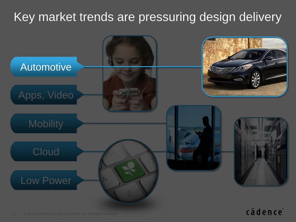
Key market trends are pressuring design delivery
Apps, Video
Mobility
Cloud
Low Power
Automotive
Key market trends are pressuring design delivery
Page 3
3 © 2012 Cadence Design Systems, Inc. All rights reserved.
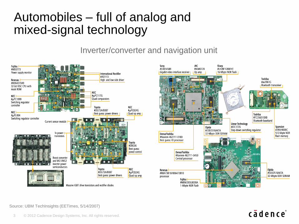
Automobiles – full of analog and mixed-signal technology
Source: UBM TechInsights (EETimes, 5/14/2007)
Inverter/converter and navigation unit
Page 4
4 © 2012 Cadence Design Systems, Inc. All rights reserved.
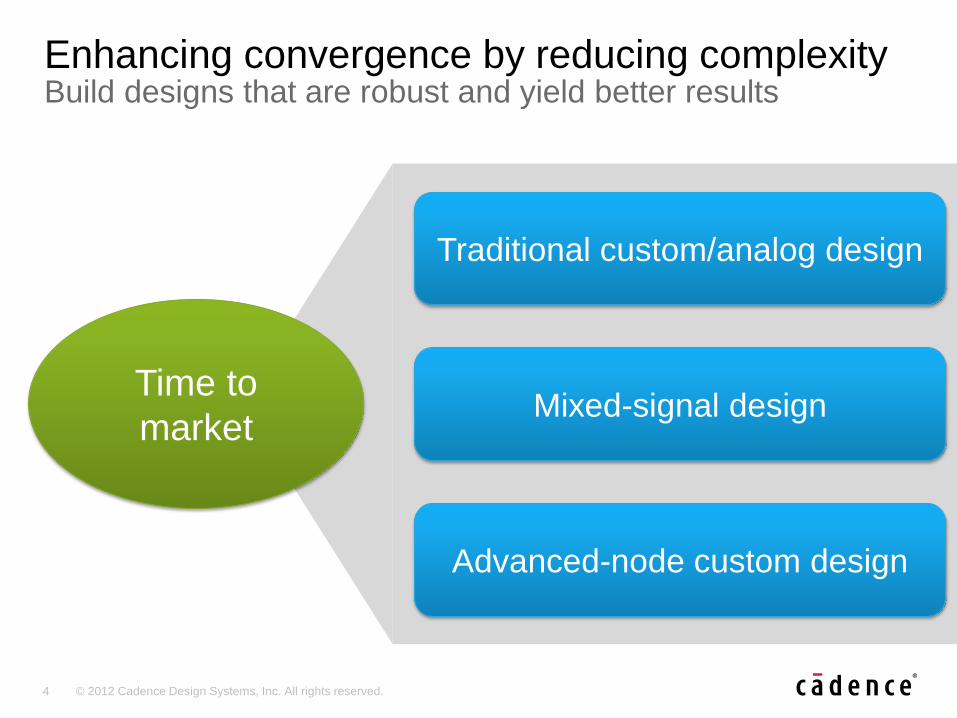
Enhancing convergence by reducing complexity Build designs that are robust and yield better results
Traditional custom/analog design
Mixed-signal design
Advanced-node custom design
Time to
market
Page 5
5 © 2012 Cadence Design Systems, Inc. All rights reserved.
Traditional custom/analog design
Page 6
6 © 2012 Cadence Design Systems, Inc. All rights reserved.
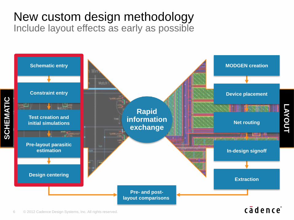
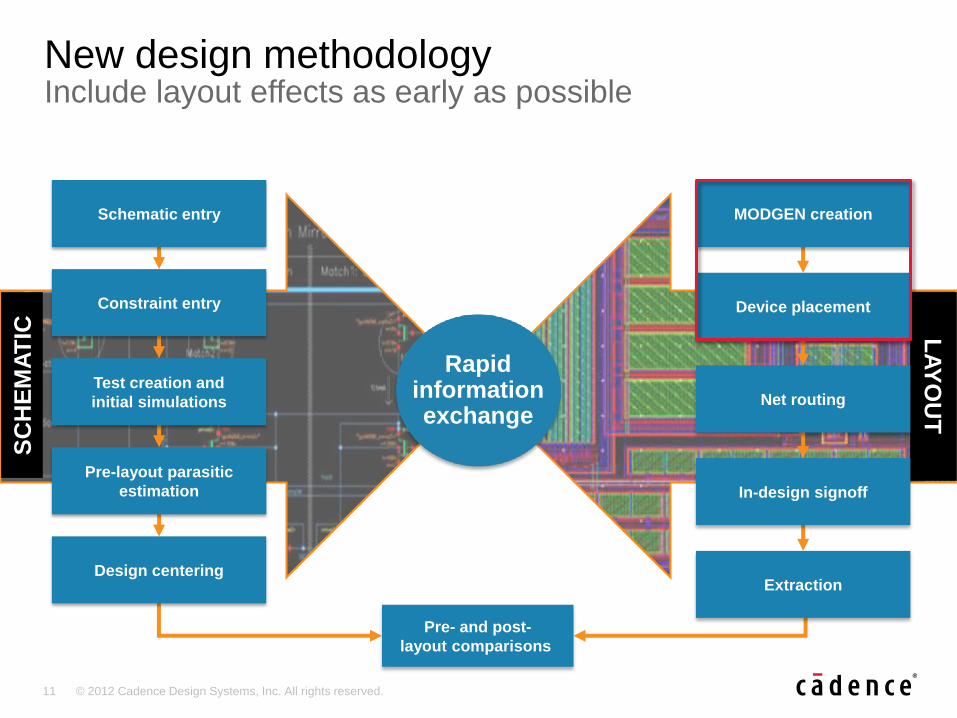
New custom design methodology Include layout effects as early as possible
Pre- and post-
layout comparisons
MODGEN creation
Device placement
In-design signoff
Net routing
Extraction
SC
HE
MA
TIC
Constraint entry
Pre-layout parasitic
estimation
Test creation and
initial simulations
Design centering
Schematic entry
Rapid information exchange
LA
YO
UT
Page 7
7 © 2012 Cadence Design Systems, Inc. All rights reserved.
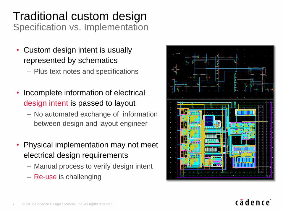
Traditional custom design Specification vs. Implementation
• Custom design intent is usually
represented by schematics
– Plus text notes and specifications
• Incomplete information of electrical
design intent is passed to layout
– No automated exchange of information
between design and layout engineer
• Physical implementation may not meet
electrical design requirements
– Manual process to verify design intent
– Re-use is challenging
Page 8
8 © 2012 Cadence Design Systems, Inc. All rights reserved.
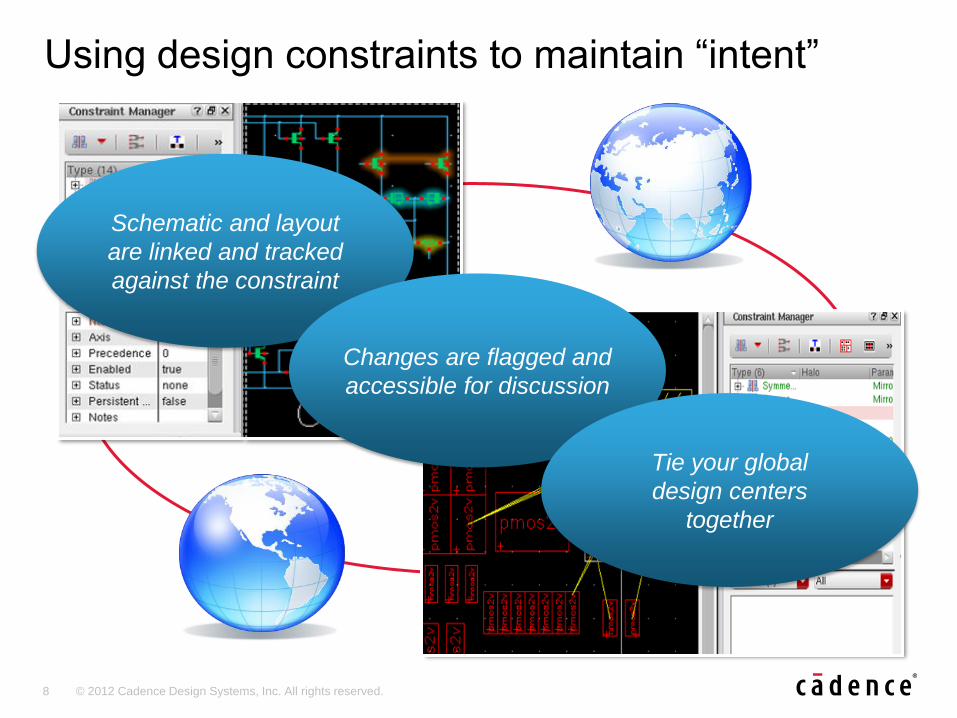
Using design constraints to maintain “intent”
Schematic and layout
are linked and tracked
against the constraint
Changes are flagged and
accessible for discussion
Tie your global
design centers
together
Page 9
9 © 2012 Cadence Design Systems, Inc. All rights reserved.
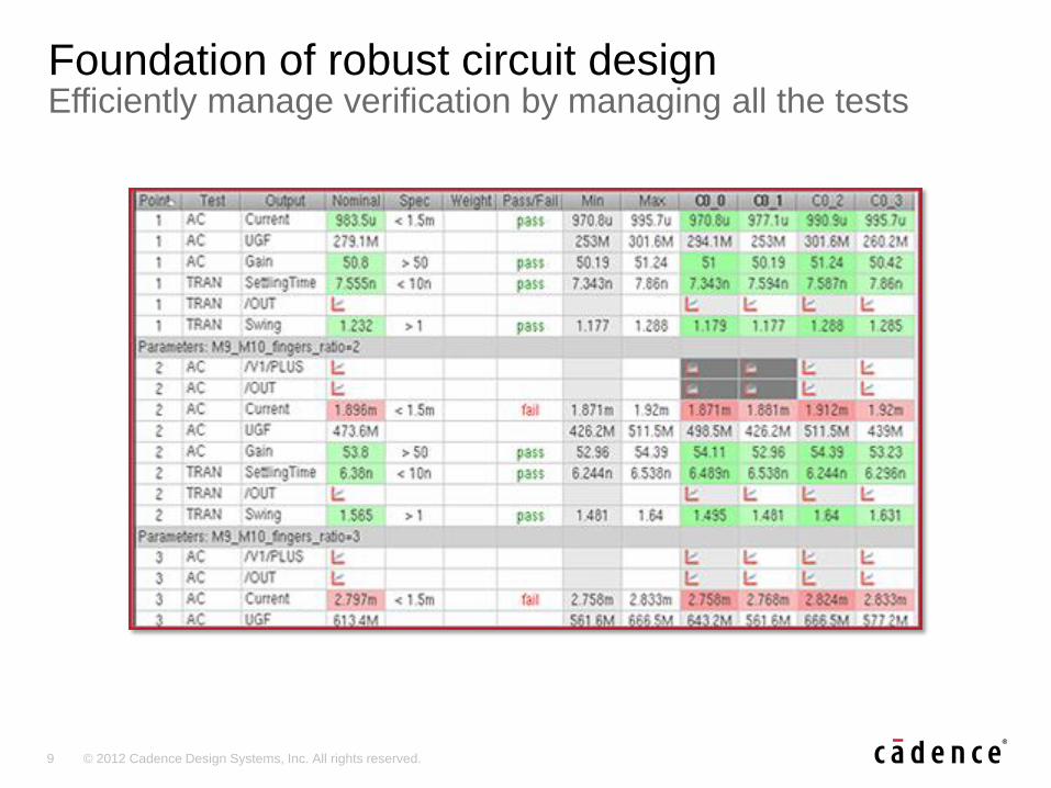
Foundation of robust circuit design Efficiently manage verification by managing all the tests
Page 10
10 © 2012 Cadence Design Systems, Inc. All rights reserved.
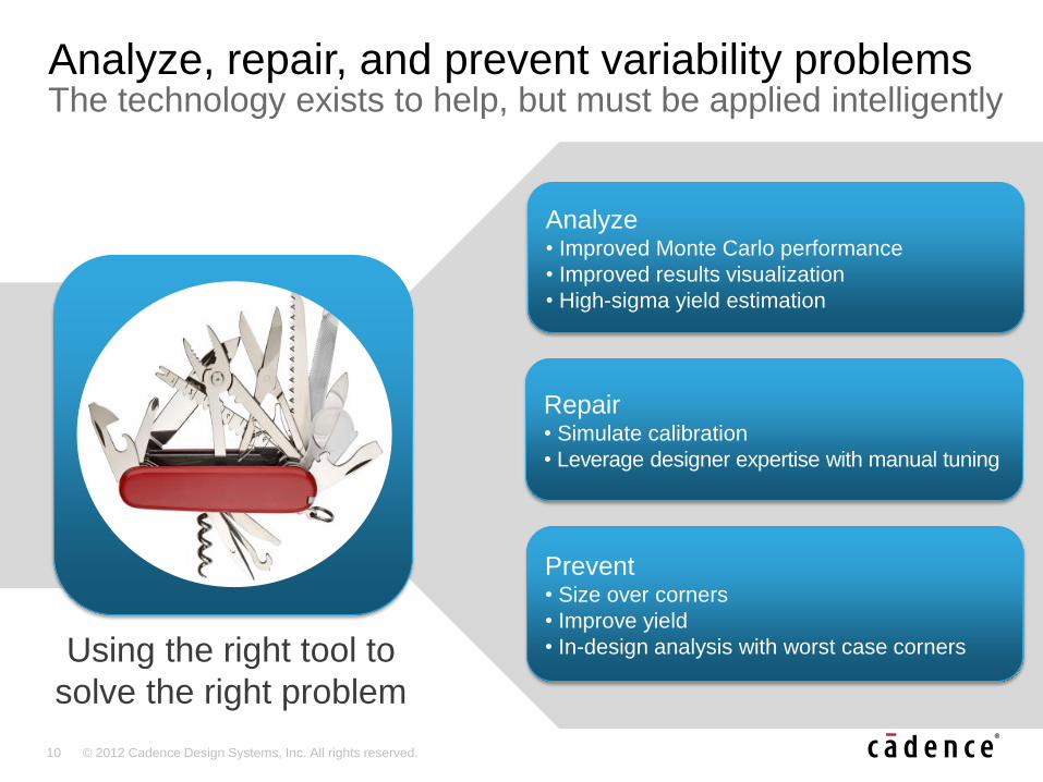
Analyze, repair, and prevent variability problems The technology exists to help, but must be applied intelligently
Analyze
• Improved Monte Carlo performance
• Improved results visualization
• High-sigma yield estimation
Repair • Simulate calibration
• Leverage designer expertise with manual tuning
Prevent • Size over corners
• Improve yield
• In-design analysis with worst case corners Using the right tool to
solve the right problem
Page 11
11 © 2012 Cadence Design Systems, Inc. All rights reserved.
New design methodology Include layout effects as early as possible
Pre- and post-
layout comparisons
SC
HE
MA
TIC
Constraint entry
Pre-layout parasitic
estimation
Test creation and
initial simulations
Design centering
Schematic entry
Rapid information exchange
LA
YO
UT
MODGEN creation
Device placement
In-design signoff
Net routing
Extraction
Page 12
12 © 2012 Cadence Design Systems, Inc. All rights reserved.
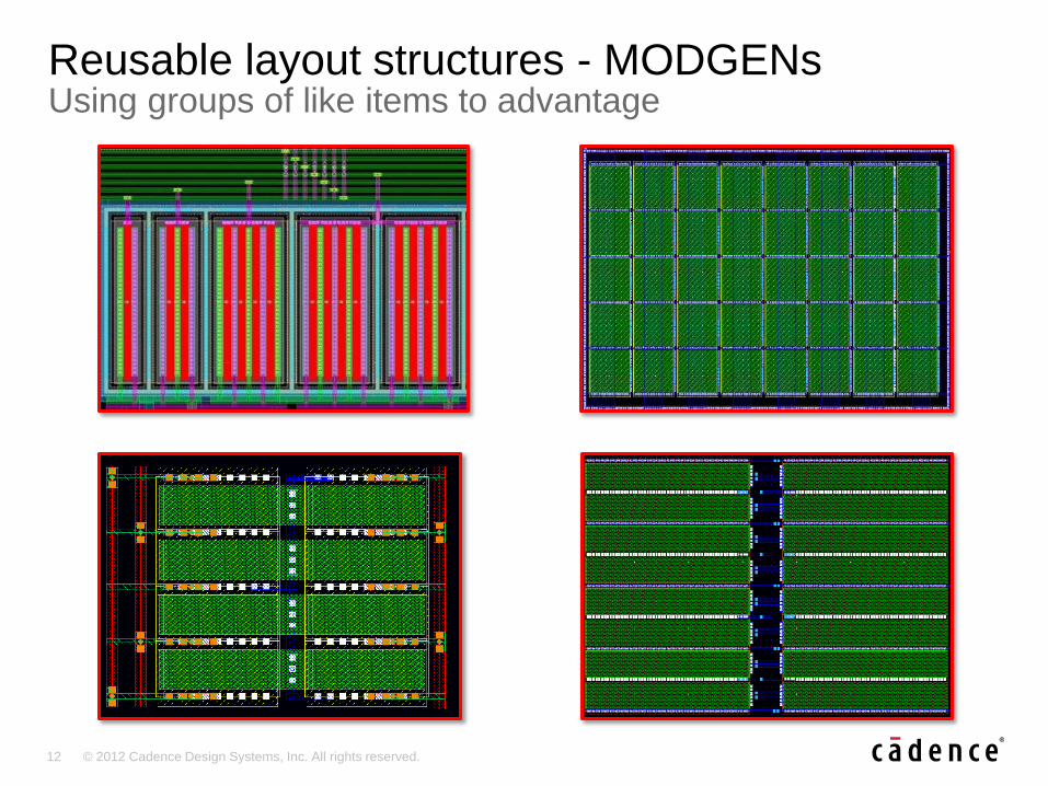
Reusable layout structures - MODGENs Using groups of like items to advantage
Page 13
13 © 2012 Cadence Design Systems, Inc. All rights reserved.
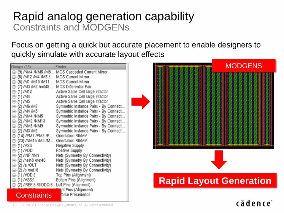
Rapid analog generation capability Constraints and MODGENs
MODGENS
Rapid Layout Generation
Focus on getting a quick but accurate placement to enable designers to
quickly simulate with accurate layout effects
Constraints
Page 14
14 © 2012 Cadence Design Systems, Inc. All rights reserved.
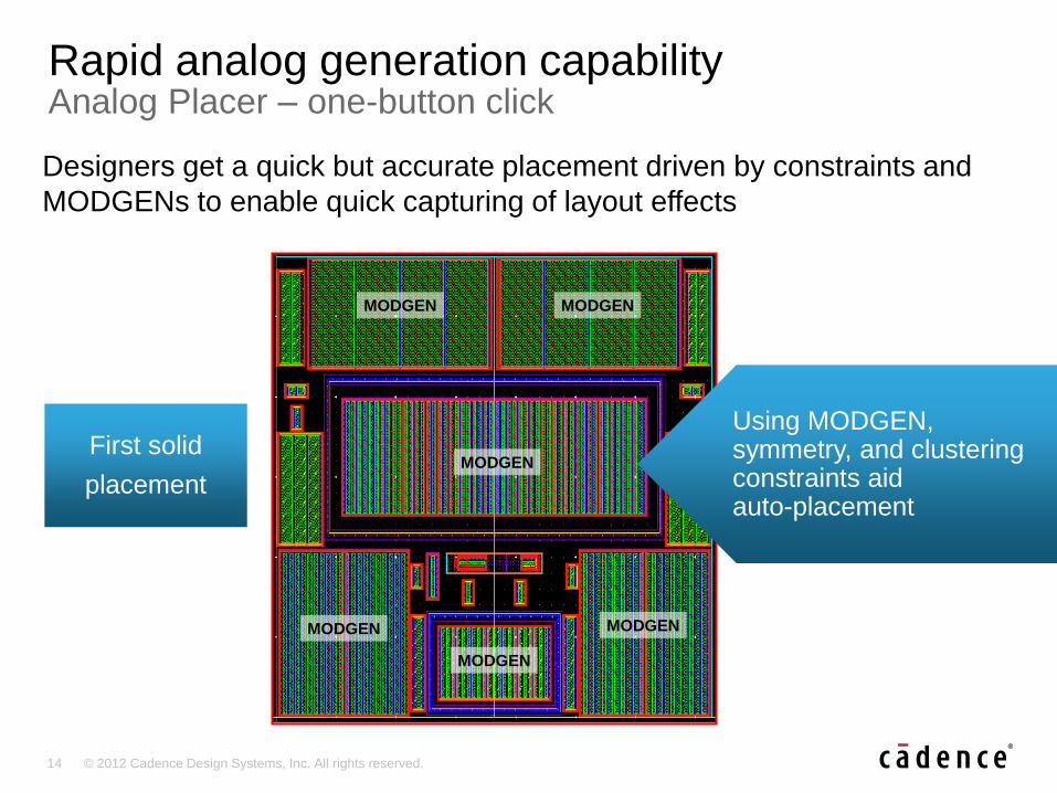
Designers get a quick but accurate placement driven by constraints and
MODGENs to enable quick capturing of layout effects
Rapid analog generation capability Analog Placer – one-button click
First solid
placement MODGEN
MODGEN MODGEN
MODGEN
MODGEN MODGEN
Using MODGEN, symmetry, and clustering constraints aid auto-placement
Page 15
15 © 2012 Cadence Design Systems, Inc. All rights reserved.
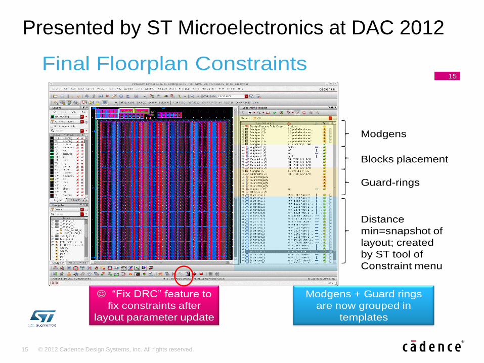
Final Floorplan Constraints15
“Fix DRC” feature to
fix constraints after
layout parameter update
Modgens
Guard-rings
Distance
min=snapshot of
layout; created
by ST tool of
Constraint menu
Blocks placement
Modgens + Guard rings
are now grouped in
templates
Presented by ST Microelectronics at DAC 2012
Page 16
16 © 2012 Cadence Design Systems, Inc. All rights reserved.
Mixed-signal design
Page 17
17 © 2012 Cadence Design Systems, Inc. All rights reserved.
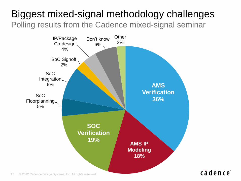
Biggest mixed-signal methodology challenges Polling results from the Cadence mixed-signal seminar
AMS Verification
36%
AMS IP Modeling
18%
SOC Verification
19%
SoC Floorplanning
5%
SoC Integration
8%
SoC Signoff 2%
IP/Package Co-design
4%
Don’t know 6%
Other 2%
Page 18
18 © 2012 Cadence Design Systems, Inc. All rights reserved.
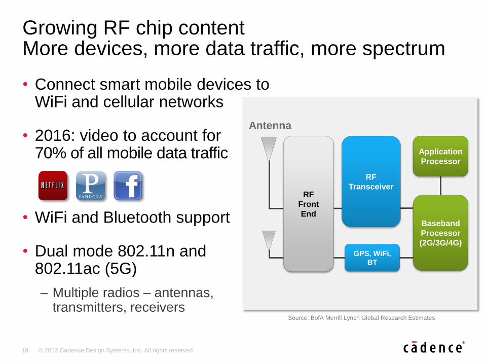
• Connect smart mobile devices to WiFi and cellular networks
• 2016: video to account for 70% of all mobile data traffic
• WiFi and Bluetooth support
• Dual mode 802.11n and 802.11ac (5G)
– Multiple radios – antennas, transmitters, receivers
Growing RF chip content More devices, more data traffic, more spectrum
RF
Transceiver
Application
Processor
Baseband
Processor
(2G/3G/4G)
GPS, WiFi,
BT
RF
Front
End
Antenna
Source: BofA Merrill Lynch Global Research Estimates
Page 19
19 © 2012 Cadence Design Systems, Inc. All rights reserved.
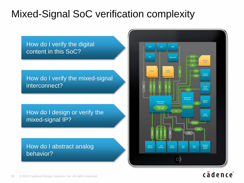
Mixed-Signal SoC verification complexity
How do I design or verify the
mixed-signal IP?
How do I verify the mixed-signal
interconnect?
How do I verify the digital
content in this SoC?
How do I abstract analog
behavior?
LPDDR DRAM
NAND
FLASH
NAND
FLASH
External
Display
Driver
USB
Interface
Test
Port
Trace
Port
Cell WiFi
Dig
RF
LP
DD
R 2
eM
MC
UF
S
LP
DD
R 3
SLIMbus
Audio
Interface
Display
Driver
CSI2
CSI3
Bluetooth FM
GPS
RF
FE
SL
IMb
us
Motion
Sensors
GBT
SP
MI
Power
Control
Multimedia
Processor
OCP 2.0, 3.0
I2C
Applications
Processor
AMBA4 ACE, AXI, AHB
Touch
Screen
Controller
Camera
Interface
UFS
SD 4.0
SD 3.0
Memory
Card
cJTAG US
B 2
.0
US
B O
TG
US
B 3
.0
HDMI
DSI
LLI
SD
IO
Page 20
20 © 2012 Cadence Design Systems, Inc. All rights reserved.
So is it possible to verify your circuit without getting wrapped up in the gears?
Yes, but one size
doesn’t fit all…
Page 21
21 © 2012 Cadence Design Systems, Inc. All rights reserved.
Productivity optimized Mixed-Signal Solution
Automated interaction
via OpenAccess
Analo
g-c
entric
mix
ed-s
ignal
Dig
ital-c
entric
mix
ed-s
ignal
Page 22
22 © 2012 Cadence Design Systems, Inc. All rights reserved.
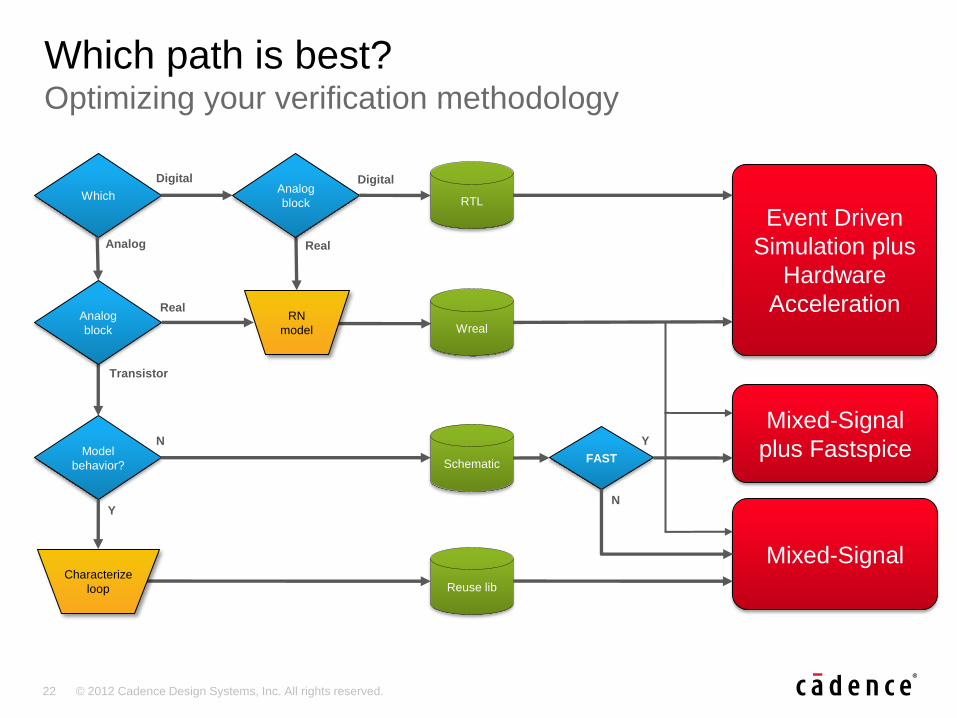
Which path is best? Optimizing your verification methodology
Which
Event Driven
Simulation plus
Hardware
Acceleration
Mixed-Signal
Digital
Analog
Model
behavior?
Reuse lib Characterize
loop
Transistor
Y
RN
model Wreal
Real
Analog
block RTL
Digital
Mixed-Signal
plus Fastspice Schematic FAST
N
N
Y
Real Analog
block
Page 23
23 © 2012 Cadence Design Systems, Inc. All rights reserved.
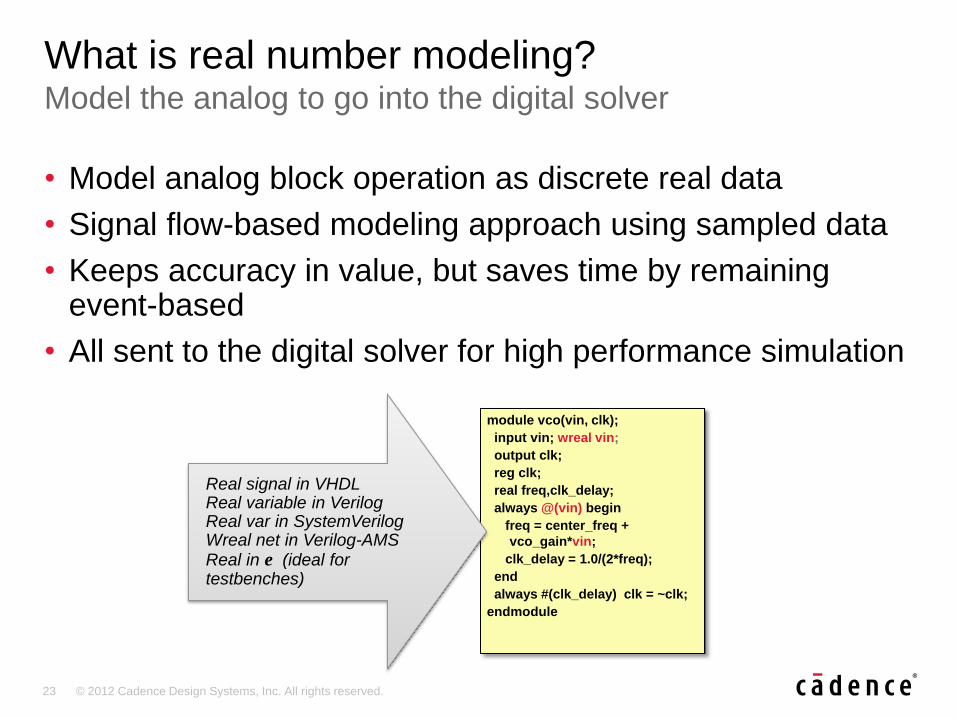
• Model analog block operation as discrete real data
• Signal flow-based modeling approach using sampled data
• Keeps accuracy in value, but saves time by remaining event-based
• All sent to the digital solver for high performance simulation
What is real number modeling? Model the analog to go into the digital solver
module vco(vin, clk);
input vin; wreal vin;
output clk;
reg clk;
real freq,clk_delay;
always @(vin) begin
freq = center_freq +
vco_gain*vin;
clk_delay = 1.0/(2*freq);
end
always #(clk_delay) clk = ~clk;
endmodule
Real signal in VHDL Real variable in Verilog Real var in SystemVerilog Wreal net in Verilog-AMS Real in e (ideal for testbenches)
Page 24
24 © 2012 Cadence Design Systems, Inc. All rights reserved.
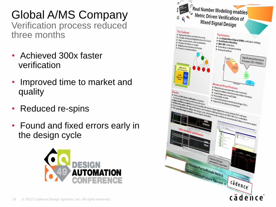
• Achieved 300x faster verification
• Improved time to market and quality
• Reduced re-spins
• Found and fixed errors early in the design cycle
Global A/MS Company Verification process reduced three months
Page 25
25 © 2012 Cadence Design Systems, Inc. All rights reserved.
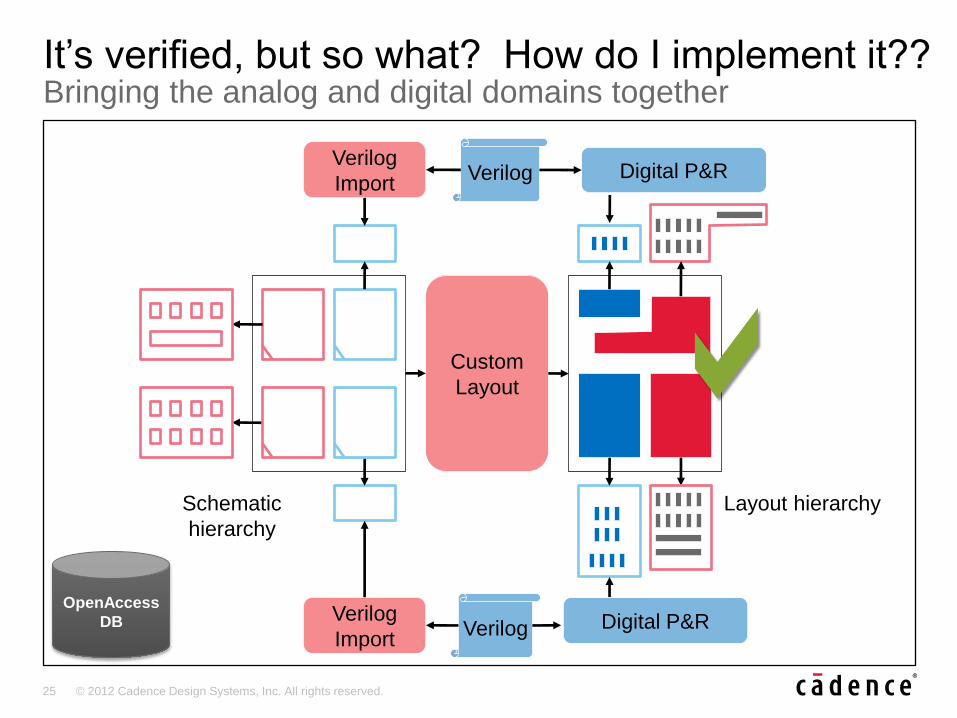
It’s verified, but so what? How do I implement it?? Bringing the analog and digital domains together
Verilog
Import
Verilog
Import
Custom
Layout
Verilog Digital P&R
Verilog
Schematic
hierarchy
Layout hierarchy
OpenAccess
DB Digital P&R
Page 26
26 © 2012 Cadence Design Systems, Inc. All rights reserved.
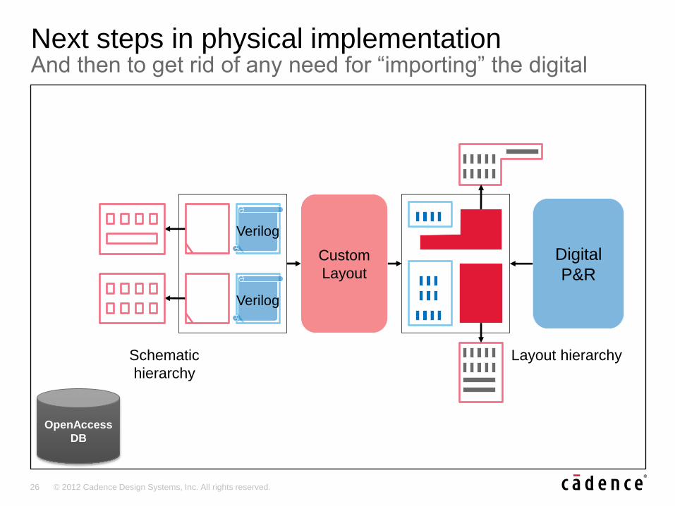
Next steps in physical implementation And then to get rid of any need for “importing” the digital
Verilog
Verilog
Schematic
hierarchy
Layout hierarchy
Digital
P&R
Custom
Layout
OpenAccess
DB
Page 27
27 © 2012 Cadence Design Systems, Inc. All rights reserved.
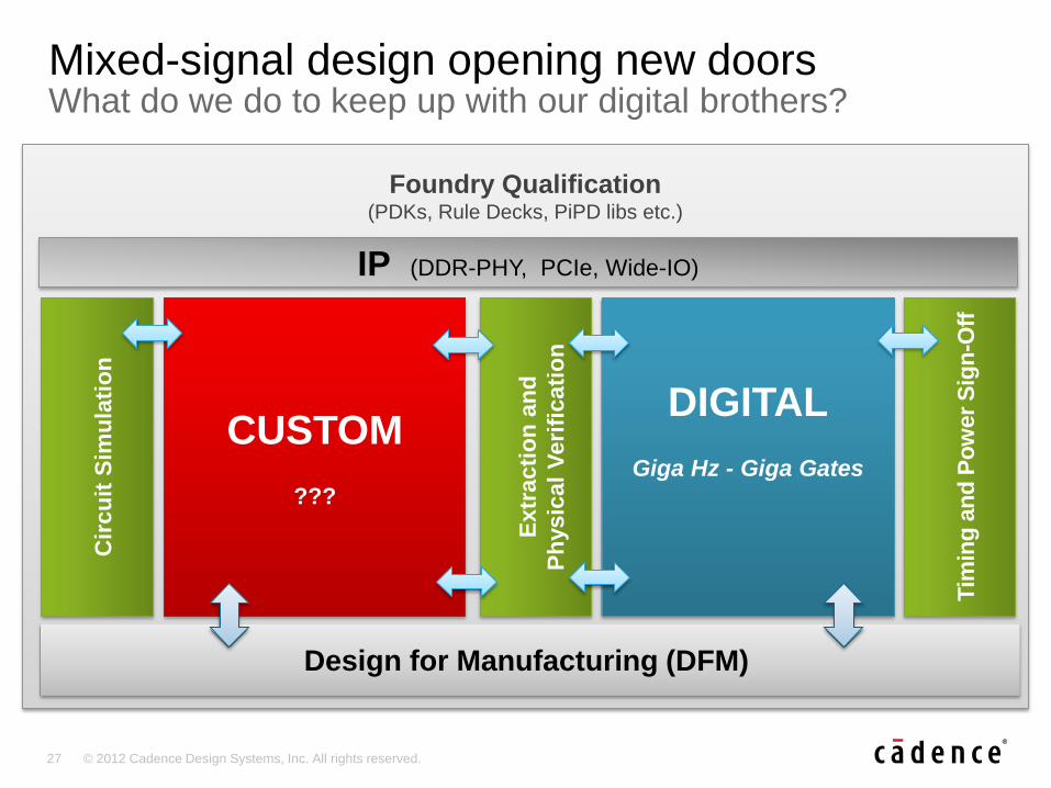
Mixed-signal design opening new doors What do we do to keep up with our digital brothers?
Foundry Qualification (PDKs, Rule Decks, PiPD libs etc.)
CUSTOM
???
DIGITAL
Giga Hz - Giga Gates
Design for Manufacturing (DFM)
IP (DDR-PHY, PCIe, Wide-IO)
C
ircu
it S
imu
lati
on
Ex
tra
cti
on
an
d
Ph
ysic
al
Veri
ficati
on
Tim
ing
an
d P
ow
er
Sig
n-O
ff
Page 28
28 © 2012 Cadence Design Systems, Inc. All rights reserved.
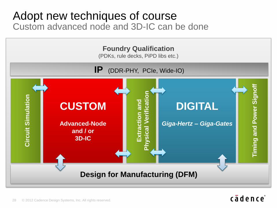
Adopt new techniques of course Custom advanced node and 3D-IC can be done
Foundry Qualification (PDKs, rule decks, PiPD libs etc.)
CUSTOM
Advanced-Node
and / or
3D-IC
DIGITAL
Giga-Hertz – Giga-Gates
Design for Manufacturing (DFM)
IP (DDR-PHY, PCIe, Wide-IO)
C
ircu
it S
imu
lati
on
Ex
tra
cti
on
an
d
Ph
ysic
al
Veri
ficati
on
Tim
ing
an
d P
ow
er
Sig
no
ff
Page 29
29 © 2012 Cadence Design Systems, Inc. All rights reserved.
Advanced-node design
Page 30
30 © 2012 Cadence Design Systems, Inc. All rights reserved.
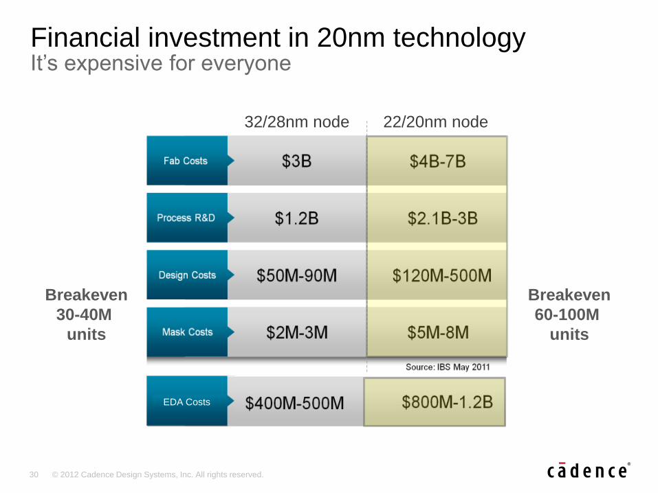
Financial investment in 20nm technology It’s expensive for everyone
Breakeven
30-40M
units
Breakeven
60-100M
units
32/28nm node 22/20nm node
EDA Costs
Page 31
31 © 2012 Cadence Design Systems, Inc. All rights reserved.
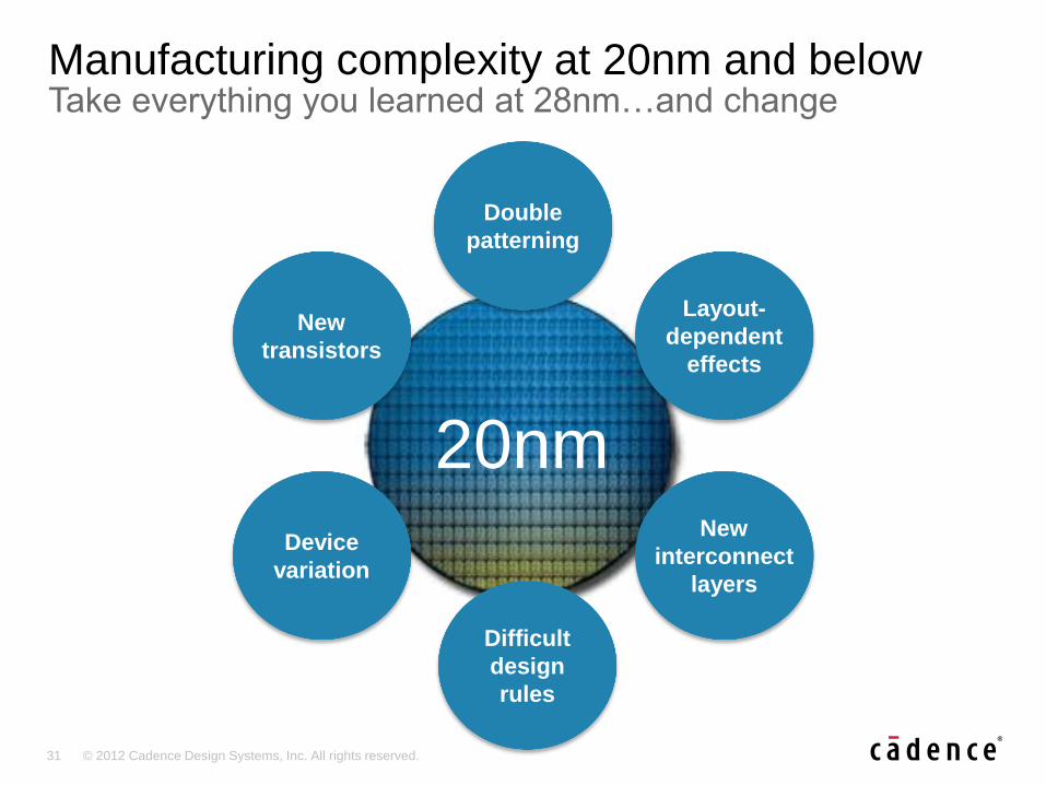
Manufacturing complexity at 20nm and below Take everything you learned at 28nm…and change
20nm
Double
patterning
Layout-
dependent
effects
New
interconnect
layers
Difficult
design
rules
Device
variation
New
transistors
Page 32
32 © 2012 Cadence Design Systems, Inc. All rights reserved.
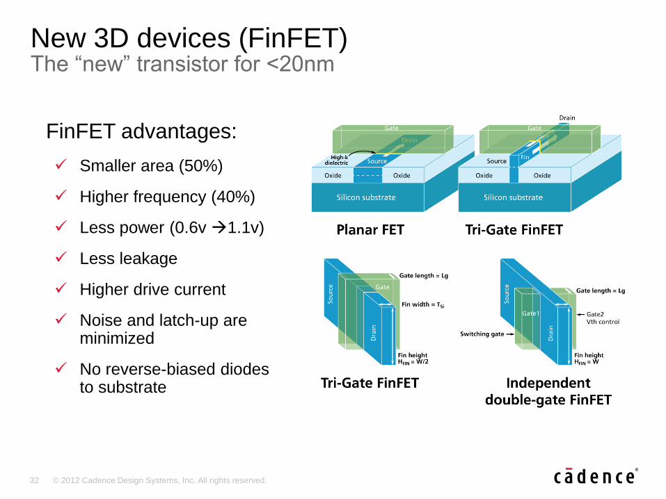
FinFET advantages:
Smaller area (50%)
Higher frequency (40%)
Less power (0.6v 1.1v)
Less leakage
Higher drive current
Noise and latch-up are minimized
No reverse-biased diodes to substrate
New 3D devices (FinFET) The “new” transistor for <20nm
Page 33
33 © 2012 Cadence Design Systems, Inc. All rights reserved.
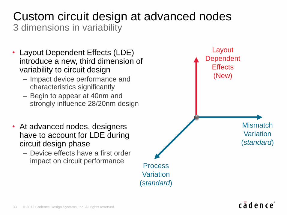
• Layout Dependent Effects (LDE) introduce a new, third dimension of variability to circuit design – Impact device performance and
characteristics significantly
– Begin to appear at 40nm and strongly influence 28/20nm design
• At advanced nodes, designers have to account for LDE during circuit design phase – Device effects have a first order
impact on circuit performance
Custom circuit design at advanced nodes 3 dimensions in variability
Layout
Dependent
Effects
(New)
Process
Variation
(standard)
Mismatch
Variation
(standard)
Page 34
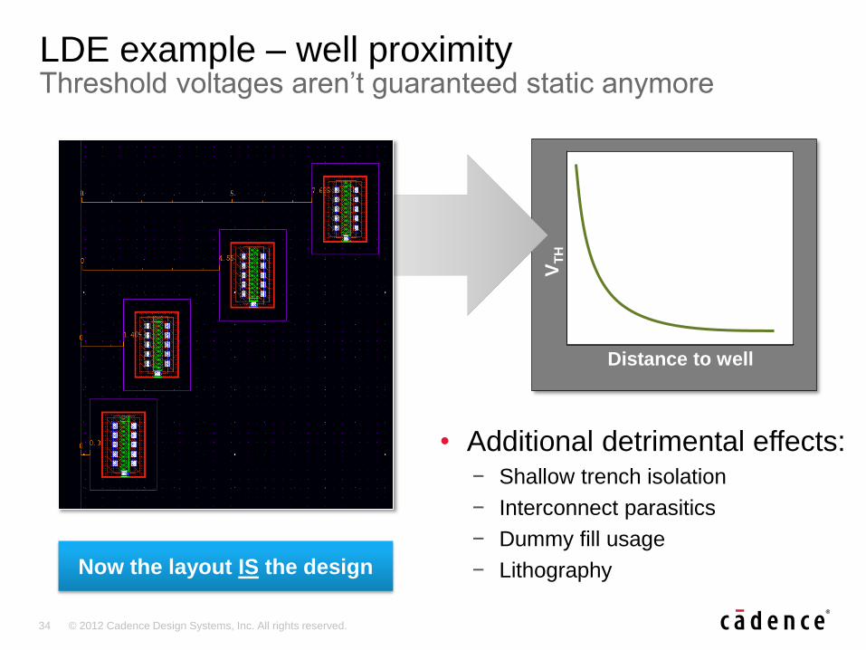
34 © 2012 Cadence Design Systems, Inc. All rights reserved.
VT
H
Distance to well
• Additional detrimental effects: − Shallow trench isolation
− Interconnect parasitics
− Dummy fill usage
− Lithography
LDE example – well proximity effect Threshold voltages aren’t guaranteed static anymore
Now the layout IS the design
Page 35
35 © 2012 Cadence Design Systems, Inc. All rights reserved.
More to do on bigger data sets Estimations are used to cut corners
Pre-layout
Schematic
Full-layout
DRC clean
Corners
Monte Carlo
Sensitivity
Parasitics
Lithography
Design Rules
• Working with layout gives the exact information but is cumbersome and it’s time consuming waiting for a full DRC layout to get information back to the designer
• Working with the schematic is fast but assumptions are made about the layout. Assumptions that don’t hold up as well at advanced nodes
?
Page 36
36 © 2012 Cadence Design Systems, Inc. All rights reserved.
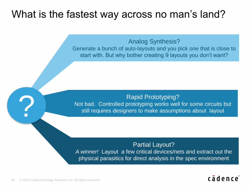
Partial Layout? A winner! Layout a few critical devices/nets and extract out the
physical parasitics for direct analysis in the spec environment
Rapid Prototyping? Not bad. Controlled prototyping works well for some circuits but
still requires designers to make assumptions about layout
Analog Synthesis? Generate a bunch of auto-layouts and you pick one that is close to
start with. But why bother creating 9 layouts you don’t want?
What is the fastest way across no man’s land?
?
Page 37
37 © 2012 Cadence Design Systems, Inc. All rights reserved.
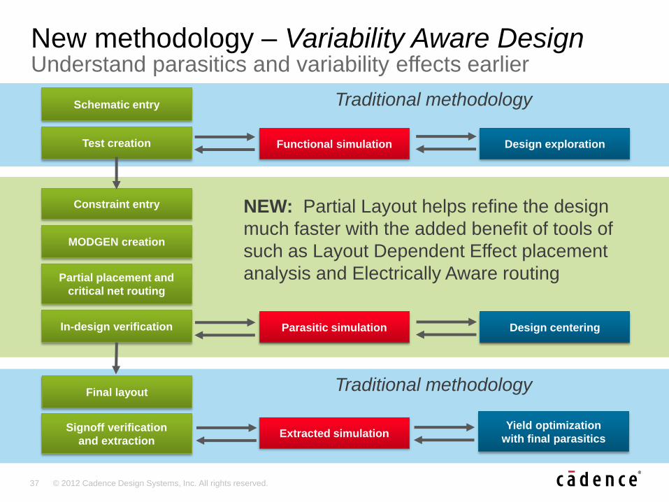
New methodology – Variability Aware Design Understand parasitics and variability effects earlier
Schematic entry
Signoff verification
and extraction
Functional simulation Test creation Design exploration
Extracted simulation Yield optimization
with final parasitics
In-design verification
Constraint entry
MODGEN creation
Partial placement and
critical net routing
Design centering Parasitic simulation
NEW: Partial Layout helps refine the design
much faster with the added benefit of tools of
such as Layout Dependent Effect placement
analysis and Electrically Aware routing
Traditional methodology
Traditional methodology Final layout
Page 38
38 © 2012 Cadence Design Systems, Inc. All rights reserved.
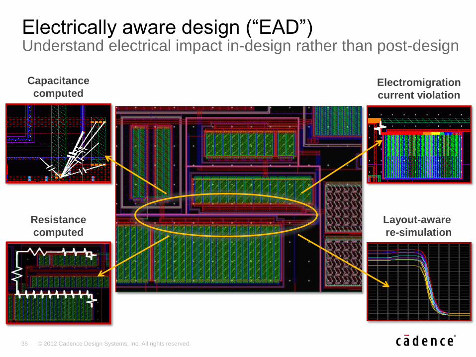
Electrically aware design (“EAD”) Understand electrical impact in-design rather than post-design
Resistance
computed
Capacitance
computed Electromigration
current violation
Layout-aware
re-simulation
Page 39
39 © 2012 Cadence Design Systems, Inc. All rights reserved.
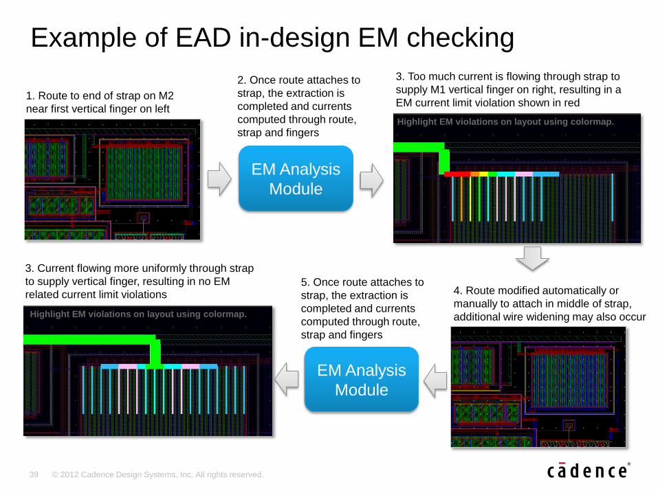
Example of EAD in-design EM checking
Highlight EM violations on layout using colormap.
Highlight EM violations on layout using colormap.
1. Route to end of strap on M2
near first vertical finger on left
3. Too much current is flowing through strap to
supply M1 vertical finger on right, resulting in a
EM current limit violation shown in red
2. Once route attaches to
strap, the extraction is
completed and currents
computed through route,
strap and fingers
4. Route modified automatically or
manually to attach in middle of strap,
additional wire widening may also occur
EM Analysis
Module
5. Once route attaches to
strap, the extraction is
completed and currents
computed through route,
strap and fingers
3. Current flowing more uniformly through strap
to supply vertical finger, resulting in no EM
related current limit violations
EM Analysis
Module
Page 40
40 © 2012 Cadence Design Systems, Inc. All rights reserved.
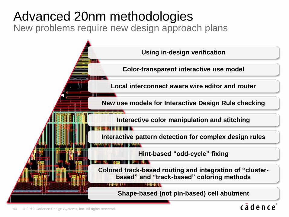
Advanced 20nm methodologies New problems require new design approach plans
Using in-design verification
Color-transparent interactive use model
Local interconnect aware wire editor and router
New use models for Interactive Design Rule checking
Interactive color manipulation and stitching
Interactive pattern detection for complex design rules
Hint-based “odd-cycle” fixing
Colored track-based routing and integration of “cluster-based” and “track-based” coloring methods
Shape-based (not pin-based) cell abutment
Page 41
41 © 2012 Cadence Design Systems, Inc. All rights reserved.
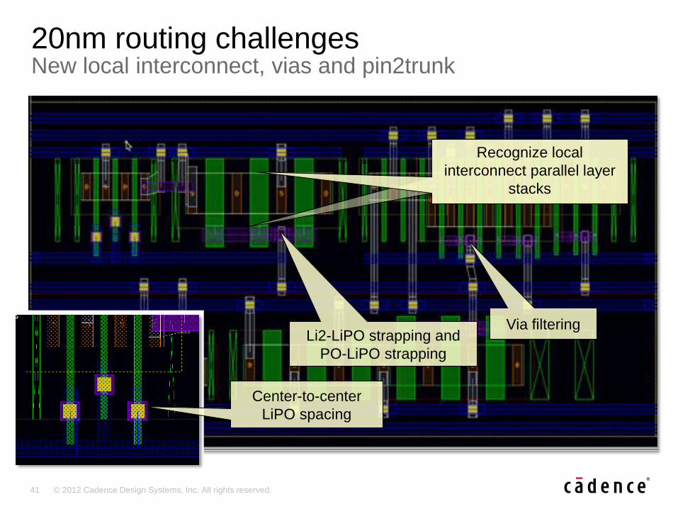
20nm routing challenges New local interconnect, vias and pin2trunk
Center-to-center
LiPO spacing
Li2-LiPO strapping and
PO-LiPO strapping
Via filtering
Recognize local
interconnect parallel layer
stacks
Page 42
42 © 2012 Cadence Design Systems, Inc. All rights reserved.
3D-IC design and analysis
Page 43
43 © 2012 Cadence Design Systems, Inc. All rights reserved.
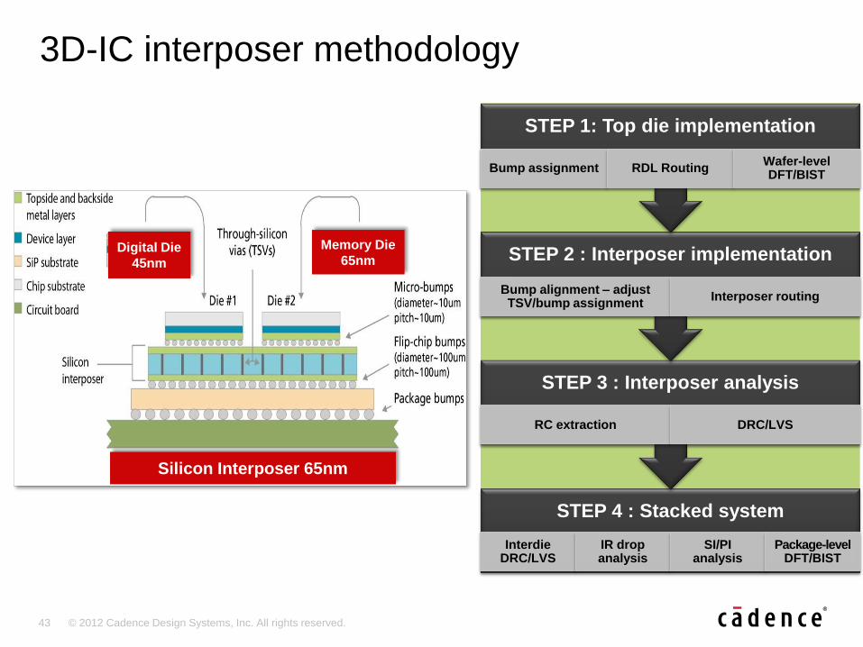
3D-IC interposer methodology
Digital Die
45nm
Memory Die
65nm
Silicon Interposer 65nm
STEP 4 : Stacked system
Interdie DRC/LVS
IR drop analysis
SI/PI analysis
Package-level DFT/BIST
STEP 3 : Interposer analysis
RC extraction DRC/LVS
STEP 2 : Interposer implementation
Bump alignment – adjust TSV/bump assignment
Interposer routing
STEP 1: Top die implementation
Bump assignment RDL Routing Wafer-level DFT/BIST
Page 44
44 © 2012 Cadence Design Systems, Inc. All rights reserved.
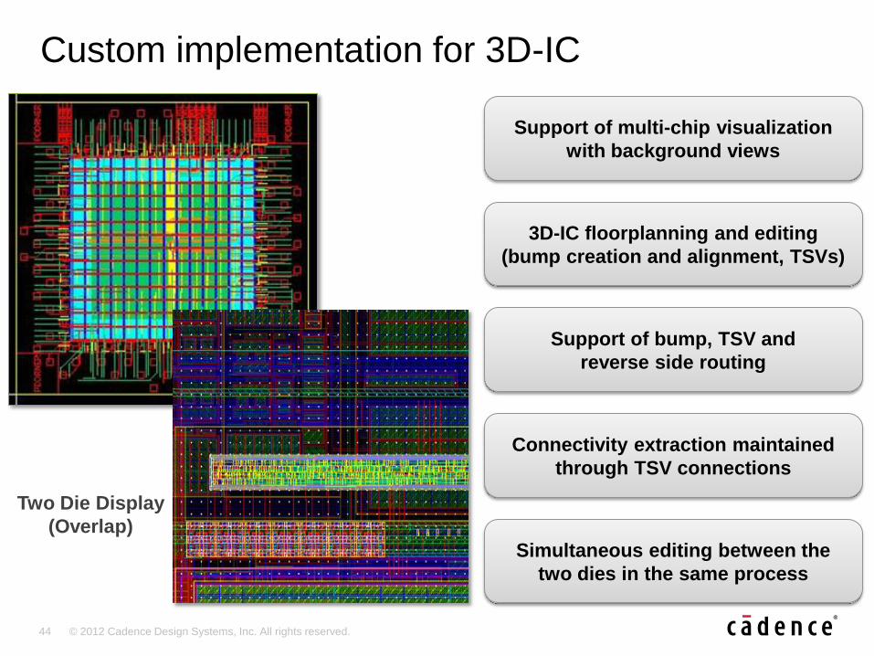
Custom implementation for 3D-IC
Support of multi-chip visualization
with background views
3D-IC floorplanning and editing
(bump creation and alignment, TSVs)
Support of bump, TSV and
reverse side routing
Connectivity extraction maintained
through TSV connections
Simultaneous editing between the
two dies in the same process
Two Die Display
(Overlap)
Page 45
45 © 2012 Cadence Design Systems, Inc. All rights reserved.
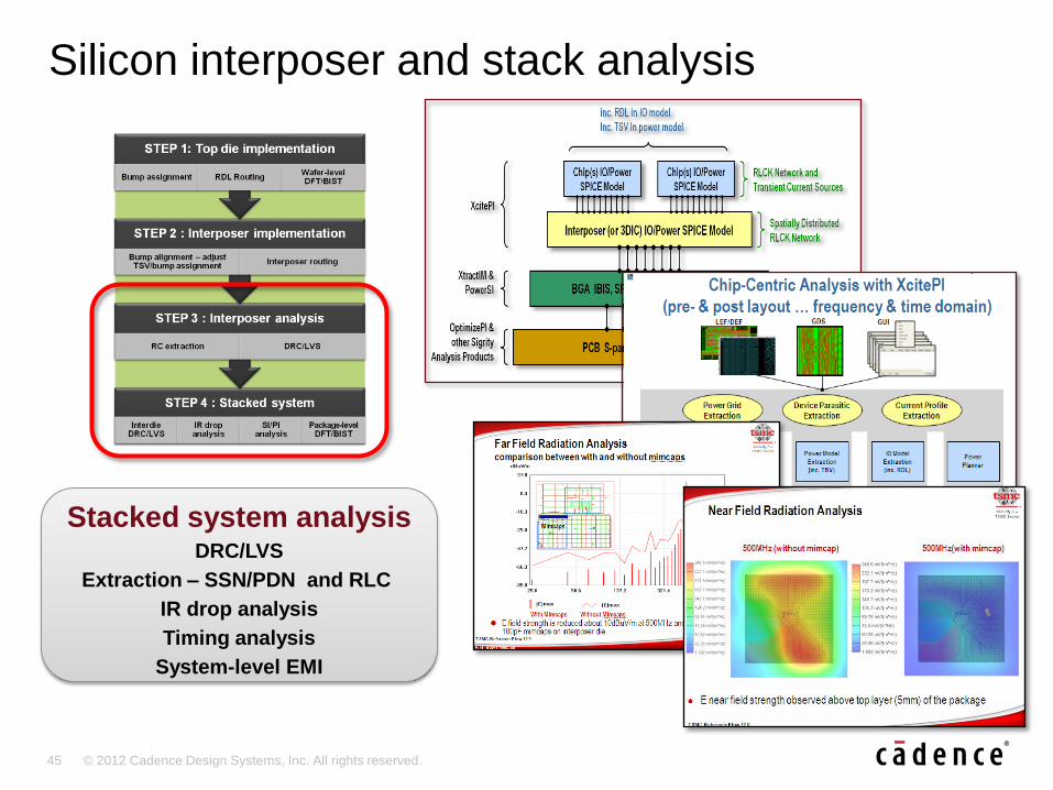
Silicon interposer and stack analysis
Stacked system analysis DRC/LVS
Extraction – SSN/PDN and RLC
IR drop analysis
Timing analysis
System-level EMI
Page 46
46 © 2012 Cadence Design Systems, Inc. All rights reserved.
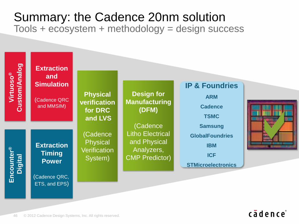
Summary: the Cadence 20nm solution Tools + ecosystem + methodology = design success
Vir
tuo
so
®
Cu
sto
m/A
na
log
En
co
un
ter®
Dig
ital
Extraction
and
Simulation
(Cadence QRC
and MMSIM)
Extraction
Timing
Power
(Cadence QRC,
ETS, and EPS)
Design for
Manufacturing
(DFM)
(Cadence
Litho Electrical
and Physical
Analyzers,
CMP Predictor)
Physical
verification
for DRC
and LVS
(Cadence
Physical
Verification
System)
IP & Foundries
ARM
Cadence
TSMC
Samsung
GlobalFoundries
IBM
ICF
STMicroelectronics
Page 47
47 © 2012 Cadence Design Systems, Inc. All rights reserved.