44
Low Power, Low Noise, Rail to Rail Fully Differential Amplifier for Class D Application ANOOP NAIR and G. S. VISWESWARAN
Low Power, Low Noise, Rail to Rail Fully Differential Amplifier for
Class D Application
ANOOP NAIR and
G. S. VISWESWARAN
10/20/11 IEP2011 2
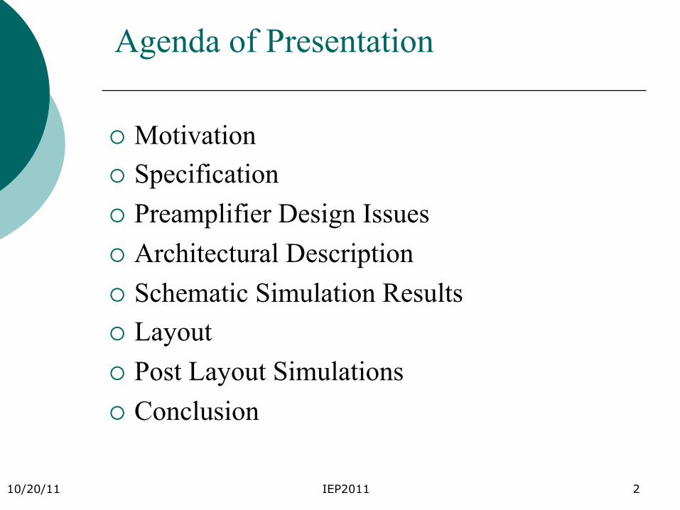
Agenda of Presentation
¡ Motivation ¡ Specification ¡ Preamplifier Design Issues ¡ Architectural Description ¡ Schematic Simulation Results ¡ Layout ¡ Post Layout Simulations ¡ Conclusion
10/20/11 IEP2011 3
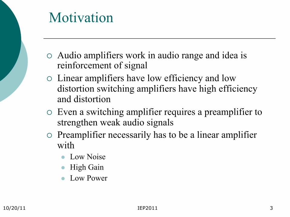
Motivation
¡ Audio amplifiers work in audio range and idea is reinforcement of signal
¡ Linear amplifiers have low efficiency and low distortion switching amplifiers have high efficiency and distortion
¡ Even a switching amplifier requires a preamplifier to strengthen weak audio signals
¡ Preamplifier necessarily has to be a linear amplifier with l Low Noise l High Gain l Low Power
10/20/11 IEP2011 4
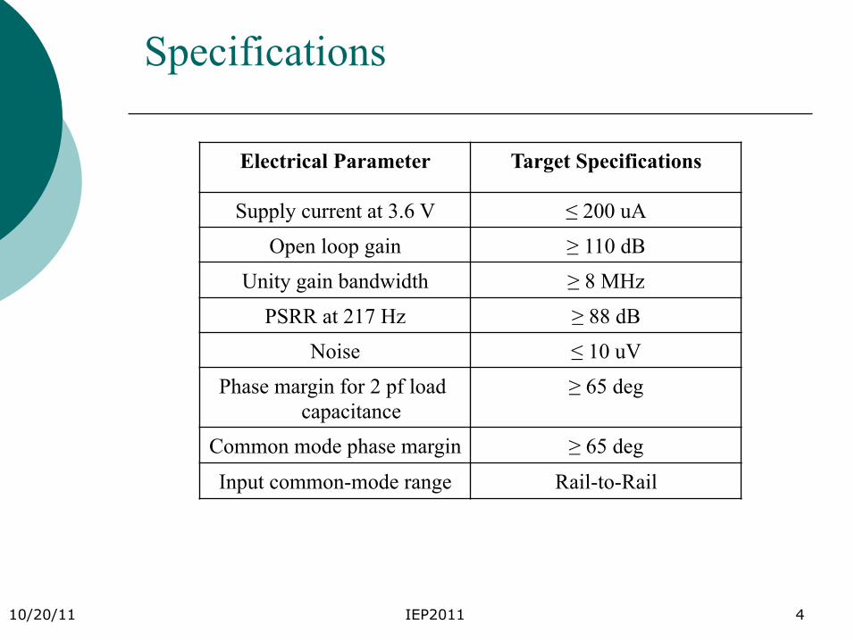
Specifications
Electrical Parameter Target Specifications
Supply current at 3.6 V ≤ 200 uA
Open loop gain ≥ 110 dB Unity gain bandwidth ≥ 8 MHz
PSRR at 217 Hz ≥ 88 dB Noise ≤ 10 uV
Phase margin for 2 pf load capacitance
≥ 65 deg
Common mode phase margin ≥ 65 deg
Input common-mode range Rail-to-Rail

10/20/11 IEP2011 5
Technology Details
Technology Node 0.5µm
Operating Voltage 3.6/5V Oxide Thickness 12.4nm Gate Oxide Capacitance 2.78e-3 F/m2 Poly resistor value 61.35 ohms / square Poly / Metal Layers 2P 4M Substrate / well formation P-sub, twin-well Poly Pitch 0.4µm
Metal Pitch 0.5 µm for ME1 0.5 µm for ME2 and ME3 0.6 µm for Top Metal
10/20/11 IEP2011 6
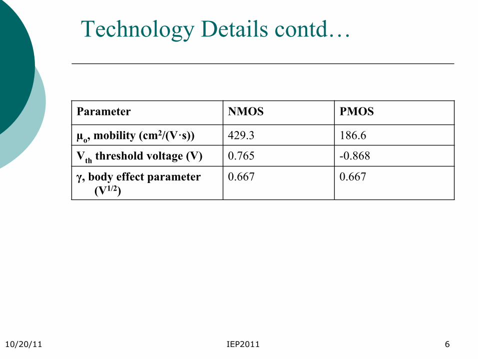
Technology Details contd…
Parameter NMOS PMOS
µo, mobility (cm2/(V·s)) 429.3 186.6
Vth threshold voltage (V) 0.765 -0.868
γ, body effect parameter (V1/2)
0.667 0.667
10/20/11 IEP2011 7
Requirement for Preamplifier
¡ Low Power ¡ High Gain ¡ Low Noise ¡ High PSRR and CMRR ¡ Rail to Rail ICMR
10/20/11 IEP2011 8
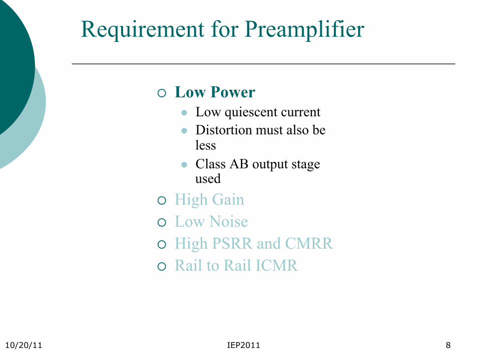
Requirement for Preamplifier
¡ Low Power l Low quiescent current l Distortion must also be
less l Class AB output stage
used ¡ High Gain ¡ Low Noise ¡ High PSRR and CMRR ¡ Rail to Rail ICMR
10/20/11 IEP2011 9
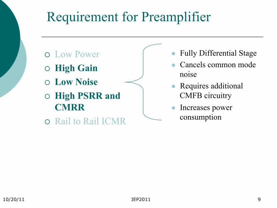
Requirement for Preamplifier
¡ Low Power ¡ High Gain ¡ Low Noise ¡ High PSRR and
CMRR ¡ Rail to Rail ICMR
l Fully Differential Stage l Cancels common mode
noise l Requires additional
CMFB circuitry l Increases power
consumption
10/20/11 IEP2011 10
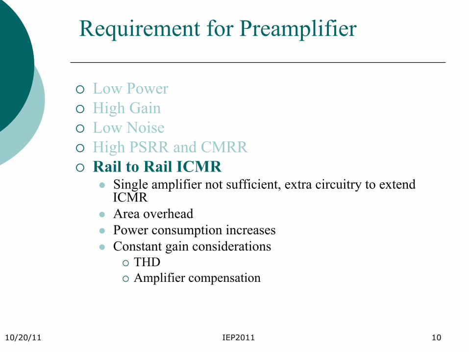
Requirement for Preamplifier
¡ Low Power ¡ High Gain ¡ Low Noise ¡ High PSRR and CMRR ¡ Rail to Rail ICMR
l Single amplifier not sufficient, extra circuitry to extend ICMR
l Area overhead l Power consumption increases l Constant gain considerations
¡ THD ¡ Amplifier compensation

10/20/11 IEP2011 11
Rail to Rail Structures- I
¡ By varying power supply for a P input amplifier
¡ Supply can be extended to compensate for VGS+ VDS drop
¡ Requires Charge Pump to raise supply

10/20/11 IEP2011 12
Rail to Rail Structures - II
¡ Use of Complementary Input stages ¡ Bias currents to input stages is varied by
sensing change in common mode voltage
Current Spillover control
Constant sum of root of tail currents
10/20/11 IEP2011 13
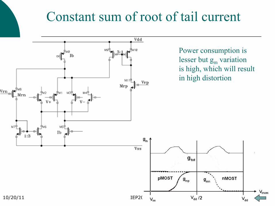
Constant sum of root of tail current
Power consumption is lesser but gm variation is high, which will result in high distortion
10/20/11 IEP2011 14
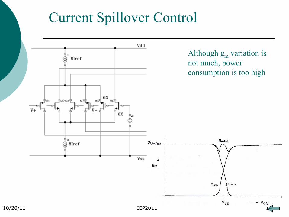
Current Spillover Control
Although gm variation is not much, power consumption is too high
10/20/11 IEP2011 15
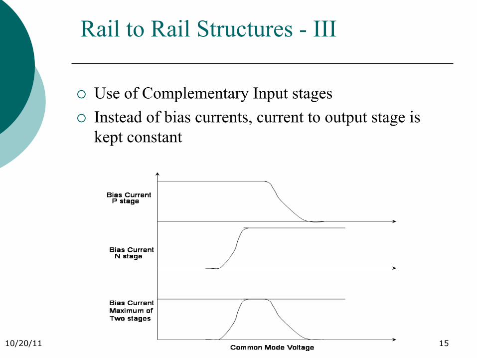
Rail to Rail Structures - III
¡ Use of Complementary Input stages ¡ Instead of bias currents, current to output stage is
kept constant

10/20/11 IEP2011 16
Rail to Rail Structures – III contd..
¡ I1 and I2 are input currents
¡ Iout = Max (I1, I2)
Reference: C.C. Hung, K. Halonen, V. Porra, and M. Ismail, “Low Voltage CMOS GM-C Filter with Rail to Rail Common Mode Voltage, ” IEEE symposium of Circuits and Systems, vol. 2, pp 921-924, Aug 1996.

10/20/11 IEP2011 17
Architecture
¡ Amplifier divided into five sub-blocks l Bias Generation l Input Stage l Maximum Current Selector Circuit l Output Stage l CMFB

10/20/11 IEP2011 18
In_n In_p
Out_1 Out_2
Vcm
vgp21 vgp11
vgn_1
vgn_2
vgp_1
vgp_2
vbias1 vbias2 vncas vpcas vbias3 vbias4 Ibias
vcmfb
Output Stage
CMFB
Max. Current Select
Bias Generation PTAT
P_INPUT N_INPUT
pwrp pwrn csd
10/20/11 IEP2011 19
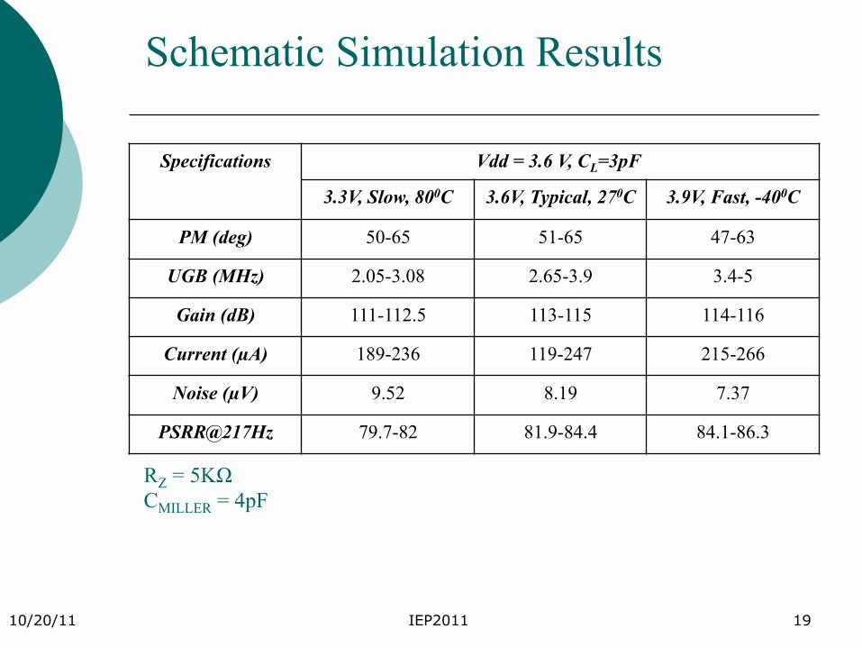
Schematic Simulation Results
Specifications Vdd = 3.6 V, CL=3pF
3.3V, Slow, 800C 3.6V, Typical, 270C 3.9V, Fast, -400C
PM (deg) 50-65 51-65 47-63
UGB (MHz) 2.05-3.08 2.65-3.9 3.4-5
Gain (dB) 111-112.5 113-115 114-116
Current (µA) 189-236 119-247 215-266
Noise (µV) 9.52 8.19 7.37
PSRR@217Hz 79.7-82 81.9-84.4 84.1-86.3
RZ = 5KΩ CMILLER = 4pF

10/20/11 IEP2011 20
Schematic Simulation Results
Specifications
Vdd = 2.6V , CL=3pF
Slow, 800C Typical, 270C Fast, -400C
PM (deg) 50.5-60 47-58 45-57
UGB (MHz) 2-2.5 2.6-3.2 3.3-4
Gain (dB) 109-110 111.5-113 113-114.5
Current (µA) 172-224 180-228 197-240
Noise (µV) 9.7 8.25 6.82
PSRR@217Hz 80.2-81.1 82.7-84.1 85.1-86
10/20/11 IEP2011 21
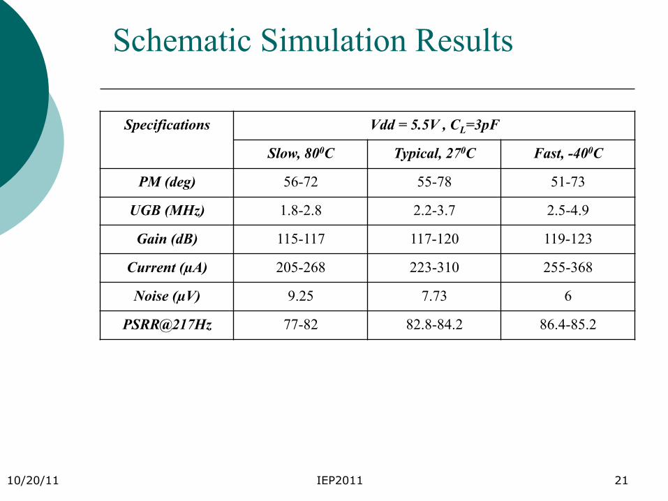
Schematic Simulation Results
Specifications Vdd = 5.5V , CL=3pF
Slow, 800C Typical, 270C Fast, -400C
PM (deg) 56-72 55-78 51-73
UGB (MHz) 1.8-2.8 2.2-3.7 2.5-4.9
Gain (dB) 115-117 117-120 119-123
Current (µA) 205-268 223-310 255-368
Noise (µV) 9.25 7.73 6
PSRR@217Hz 77-82 82.8-84.2 86.4-85.2
10/20/11 IEP2011 22
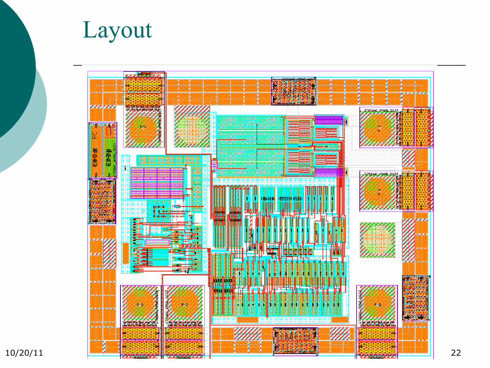
Layout

10/20/11 IEP2011 23
Pin-out
¡ Standard 8- pin SOIC ¡ IN+ IN- - inputs ¡ OUT+ OUT- - outputs ¡ VBG - bandgap
reference voltage ¡ CSD - shut down

10/20/11 IEP2011 24
Post Layout Simulations
Specifications Vdd = 3.6V, Vcm = 2.5V , CL=1pF
Slow, 800C Typical, 270C Fast, -400C
PM (deg) 55.8(65) 47.2(57.9) 69(82)
UGB (MHz) 3.6(3.95) 4.6(5.1) 4(3.5)
Gain (dB) 114(113.7) 114.6(113.8) 116.5(115.5)
Current (µA) 220(242) 240(261) 245(283)
Noise (µV) 12.1(10.4) 10.1(8.99) 8.7(8)
PSRR@217Hz 82.3(82.1) 84.7(84.44) 83.9(83.4)
RZ = 8KΩ CMILLER = 4pF

10/20/11 IEP2011 25
Post Layout Simulations
Specifications Vdd = 2.6V, Vcm = 2.5V , CL=1pF
Slow, 800C Typical, 270C Fast, -400C
PM (deg) 52.6 48.3 45.3
UGB (MHz) 2.74 3.4 4.2
Gain (dB) 112.5 113 113.6
Current (µA) 180 192 200
Noise (µV) 12.4 10.5 8.4
PSRR@217Hz 81.98 83.85 85.75

10/20/11 IEP2011 26
Post Layout Simulations
Specifications Vdd = 5.5V, Vcm = 2.5V , CL=1pF
Slow, 800C Typical, 270C Fast, -400C
PM (deg) 64.3 60.5 56.7
UGB (MHz) 2.8 3.5 4.5
Gain (dB) 121.9 124 127
Current (µA) 256 276 300
Noise (µV) 10.5 9.14 6.8
PSRR@217Hz 82.11 84.12 86.7
10/20/11 IEP2011 27
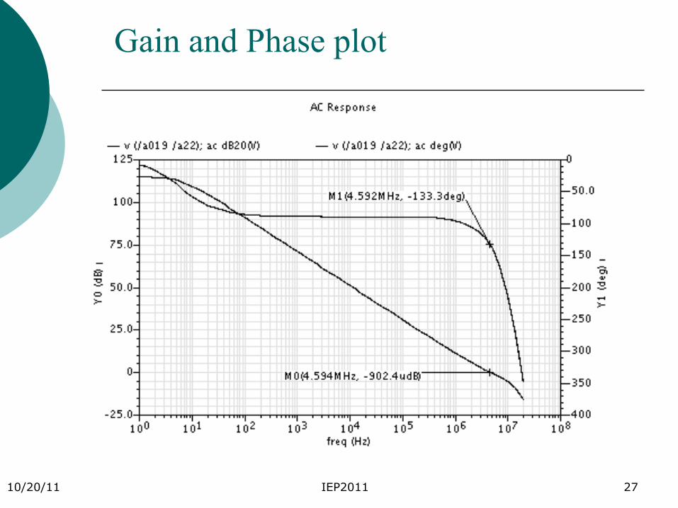
Gain and Phase plot
10/20/11 IEP2011 28
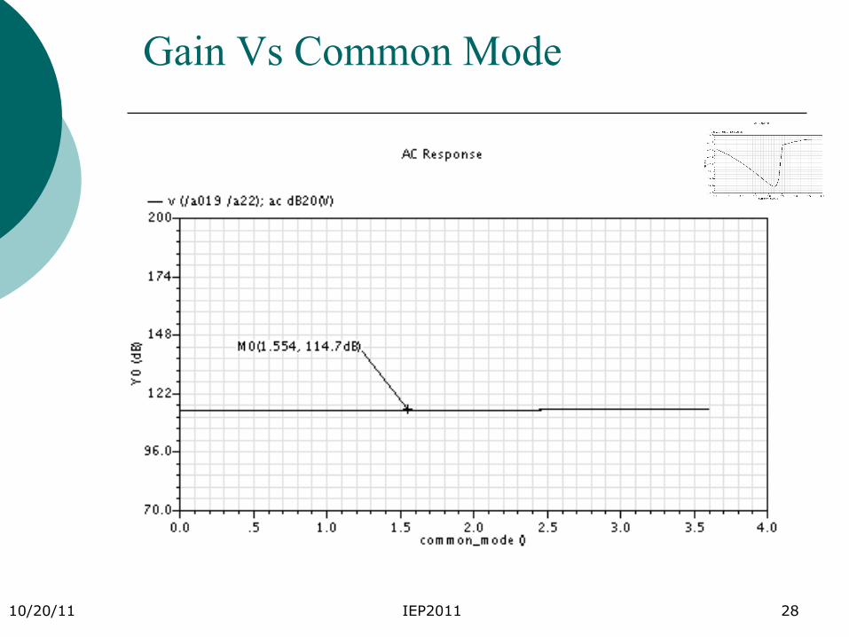
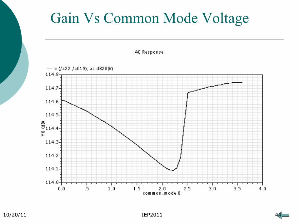
Gain Vs Common Mode
10/20/11 IEP2011 29
Conclusion
¡ Current Mirrors are noisy structures, NMOS contribute a lot of noise
¡ Noise reduction comes at the cost of power and area
¡ Power and Noise specification were met ¡ UGB and Phase Margin for some cases could
not be achieved

10/20/11 IEP2011 30
References
¡ Willy M.C. Sansen, Analog Design Essentials, Dordrecht, Netherlands; Springer, edition 2006.
¡ J.H. Huijsing, Operational Amplifiers Theory and Design; Kluwer Academic Publishers, 2001.
¡ A.F. Duisters and E.C. Dijkmans, “A -90dB THD Rail to Rail Input Opamp Using New Local Charge Pump in CMOS,” IEEE JSSC, vol. 33, pp 947-955, Jul. 1998.
¡ C.C. Hung, K. Halonen, V. Porra, and M. Ismail, “Low Voltage CMOS GM-C Filter with Rail to Rail Common Mode Voltage, ” IEEE symposium of Circuits and Systems, vol. 2, pp 921-924, Aug 1996.
¡ R. Jacob Baker, CMOS Circuit Design, Layout and Simulation, 2nd ed.; Wiley, 2004. ¡ T. Voo and C. Toumazou, “Tunable Current Mirror for High Frequency Analog
Design”, IEE colloquium on Analog Signal Processing, pp 3/1-3/14, Oct 1994. ¡ G. Ku and H.K. Embabi, “A Systematic Approach in Constructing Fully Differential
Amplifier”, IEEE Trans. On Circuits and Systems-II; Analog and Digital Signal Processing, vol. 47, pp 1343-1347, Nov. 2000.
¡ W.S. Wu, W.J. Helm, J.A. Kuhn and B.E. Byrkett, “Digital Compatible High Performance Operational Amplifier with Rail to Rail Input and Output Range,” IEEE JSSC, vol. 29, pp 63-66, Jan. 1994.
¡ Behzad Razavi, Design of Analog CMOS Integrated Circuits, TMH, edition 2002.

Thank You

10/20/11 IEP2011 32
Bias Generation

10/20/11 IEP2011 33
PTAT

10/20/11 IEP2011 34
PTAT Amplifier
10/20/11 IEP2011 35
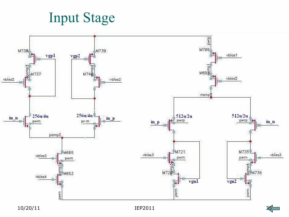
Input Stage

10/20/11 IEP2011 36
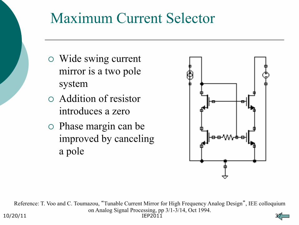
Maximum Current Selector
I1
I2
Iout
10/20/11 IEP2011 37
Maximum Current Selector
¡ Wide swing current mirror is a two pole system
¡ Addition of resistor introduces a zero
¡ Phase margin can be improved by canceling a pole
Reference: T. Voo and C. Toumazou, “Tunable Current Mirror for High Frequency Analog Design”, IEE colloquium on Analog Signal Processing, pp 3/1-3/14, Oct 1994.

10/20/11 IEP2011 38
Maximum Current Selector

10/20/11 IEP2011 39
Problems with the architecture
¡ Current Mirrors are too noisy ¡ NMOS of current mirrors are major noise
contributor ¡ High resistor is required, consuming large
area ¡ Current flows all the time causing large
power consumption
If the current can be switched off then noise as well as power consumption can be reduced

10/20/11 IEP2011 40
Switched Current Selector Circuit

10/20/11 IEP2011 41
Output Stage
10/20/11 IEP2011 42
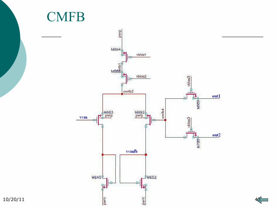
CMFB
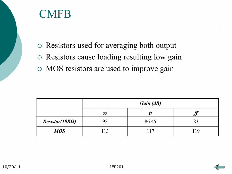
¡ Resistors used for averaging both output ¡ Resistors cause loading resulting low gain ¡ MOS resistors are used to improve gain
Gain (dB)
ss tt ff Resistor(10KΩ) 92 86.45 83
MOS 113 117 119
10/20/11 IEP2011 43
CMFB
10/20/11 IEP2011 44
Gain Vs Common Mode Voltage


