Presentation on Antireflective coatings A PRESENTED BY :- RAJNEESH KUMAR GAUTAM M-TECH (ENERGY AND ENVIRONMENT) IN THE EXPERT GUIDANCE OF :- VIJAY K. JAISWAL ASSISTANT PROFESSOR (GUEST) BBA UNIVERSITY -LUCKNOW
Transcript
Presentation
on
Antireflective coatings
A
PRESENTED BY :-
RAJNEESH KUMAR GAUTAM
M-TECH (ENERGY AND ENVIRONMENT)
IN THE EXPERT GUIDANCE OF :-
VIJAY K. JAISWAL
ASSISTANT PROFESSOR (GUEST)
BBA UNIVERSITY -LUCKNOW
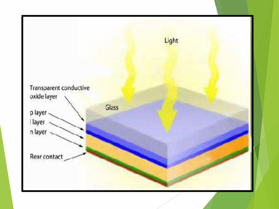
In typical installations,
approximately 4% of incoming
light is reflected off the face of
the PV module and is lost.
ANTIREFLECTION coatings
REFLECTION
coating
What is antireflective coating ?
Antireflective or anti-reflection (AR) coating is a type of optical
coating applied to the surface of lenses and other optical devices to
reduce reflection.This improves the efficiency of the system since
less light is lost.
Antireflection is achieved by destructive interference between
The rate of coating deposition is usually quite slow
CHEMICAL VAPOUR DEPOSITION
Gaseous compounds react to form a dense layer on a heated substrate. The most widely deposited wear-resistant coatings are TiC, TiN, chromium carbide and alumina. Deposition temperatures are generally in the range 800-1000C which restricts the range of materials which can be coated and can lead to component distortion. Thicknesses are limited to about 10mm due to the thermal expansion mismatch stresses which develop on cooling which also restrict the coating of sharp
edged components.
Layer deposition involves chemical reactions
Large density films
Good stoichiometry & uniformity over large surface area.
SiO2 SiN, SiON, SiOC , and TiO2 with proper thickness are
the common AR material deposited chemically.
Required high temp to produce high quality material and for
many application the substrate cannot tolerate being heated
so not useful in that case .
LIMITITATION :
Advantages
High coating hardness
Good adhesion (if the coating is not too thick)
Good throwing power (i.e. uniformity of coating)
Disadvantages
High temperature process (distortion)
Sharp edge coating is difficult (thermal expansion mismatch stresses)
Limited range of materials can be coated
Environmental concerns about process gases
Combined process of both CVD and PVD
a process used to deposit thin films from a gas state (vapour)
to a solid state on a substrate.
Chemical reactions are involved in the process, which occur after
creation of a plasma of the reacting gases
The plasma is generally created by RF (AC) frequency or DC discharge
between two electrodes, the space between which is filled with the
reacting gases.
Processing plasmas are typically operated at higher pressures
PLASMA ENHANCED CHEMICAL VAPOUR DEPOSITION
of a few millitorr to a few torr , although arc discharges and
inductive plasmas can be ignited at atmospheric pressure
Plasma enhanced CVD is most useful because it can deposit layers on fragile
substrates that cannot withstand the high temperatures of other CVD
methods
Plasma enhanced CVD systems allow for greater control of the film
composition, density, and film stress.
Higher deposition rate at low temperature relatively
Plasma can cause damage to the substrate surface when either secondary
electrons collide with the wafer surface or the energy of the ion bombard-
ment becomes too high.
High cost.
Advantages of PECVD
Disadvantages
How much reflection while using AR coating ?
Can be reduced up to ~ 0.2%
APPLICATION OF ANTIREFLECTION COATING
Anti-reflection coated optical windows
Reflex free sight glasses
Laser scanner windows
Contrast enhancement
Anti glare coated instrument windows
Sensor technology
Low reflection camera windows
Holography components
Antireflection coated glass for displays
In microelectronic photolithography to
reduce image (substrate) distortions .solar cell with SiO coating
Glass with MgF2 coating
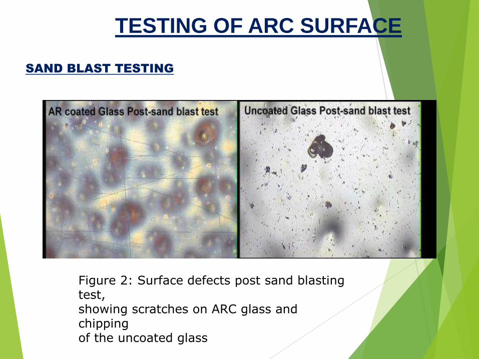
TESTING OF ARC SURFACE
SAND BLAST TESTING
Figure 2: Surface defects post sand blasting test,showing scratches on ARC glass and chippingof the uncoated glass
FMEA METHOD USED FOR ARC GLASS
Figure 1: Temporary staining due to plant residueobserved during field exposure of ARC glassmodules in heavy pollen areas in California.