www.irf.com AN-983 July 2012 1 Application Note AN-983 IGBT Characteristics Table of Contents Page 1. How the IGBT complements the power MOSFET .................................................. 2 2. Silicon structure and equivalent circuit .................................................................. 2 3. Conduction characteristics .................................................................................... 4 4. Switching characteristics ........................................................................................ 6 5. Latching ................................................................................................................. 8 6. Safe operating area ............................................................................................... 8 7. Transconductance ................................................................................................. 9 8. How to read the data sheet .................................................................................... 9 9. The IGBT technologies from IR .............................................................................. 14 10. For more information ............................................................................................ 16 IGBTs share many of the appealing features of power MOSFETs such as ease of drive, wide SOA, peak current capability and ruggedness. Being minority carrier devices they have superior conduction characteristics, at the ex- pense of switching performance. International Rectifier has an extensive line of IGBTs optimized for lowest losses in a wide range of applications.
Transcript
www.irf.com AN-983 July 2012 1
Application Note AN-983
IGBT Characteristics
Table of Contents
Page
1. How the IGBT complements the power MOSFET .................................................. 2
2. Silicon structure and equivalent circuit .................................................................. 2
8. How to read the data sheet .................................................................................... 9
9. The IGBT technologies from IR .............................................................................. 14
10. For more information ............................................................................................ 16
IGBTs share many of the appealing features of power MOSFETs such as ease of drive, wide SOA, peak current capability and ruggedness. Being minority carrier devices they have superior conduction characteristics, at the ex-pense of switching performance.
International Rectifier has an extensive line of IGBTs optimized for lowest losses in a wide range of applications.
www.irf.com AN-983 July 2012 2
1. How the IGBT complements the power MOSFET
Power MOSFETs have a number of appealing characteristics: switching speed, peak current capability, ease of drive, wide SOA, avalanche and dv/dt capability. These advantages, a natural consequence of being ma-jority carrier devices, are partly mitigated by their conduction characteristics which are strongly dependent on temperature and voltage rating. The other weakness of power MOSFETs is the fact that, as the voltage rating goes up, the reverse recovery characteristics of the integral rectifier deteriorate causing increasing switching losses.
IGBTs on the other hand, being minority carrier devices, have superior conduction characteristics, while shar-ing many of the appealing features of power MOSFETs such as ease of drive, wide SOA, peak current capa-bility and ruggedness. Generally speaking, the switching speed of an IGBT is inferior to that of power MOSFETs, even as improvements in the technology have significantly narrowed the gap.
The absence of the integral reverse diode gives the user the flexibility of choosing an external fast recovery diode to match a specific requirement or to design-in a “co-pak”, i.e. an IGBT and a diode in the same pack-age. The lack of an integral diode can be an advantage or a disadvantage, depending on the topology, fre-quency of operation, cost of diodes, current requirement, etc.
2. Silicon structure and equivalent circuit
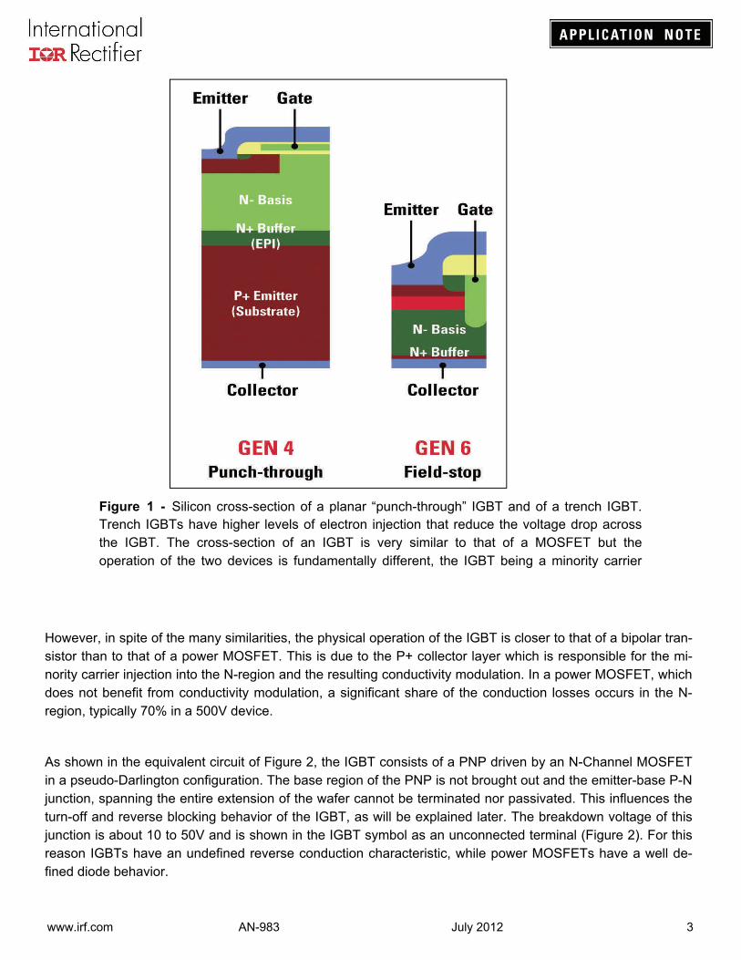
Except for the P+ layer at the bottom of die (collector), the silicon cross-section of an IGBT (Figure 1) is virtu-ally identical to that of a power MOSFET. Both devices share a similar polysilicon gate structure and P wells with N+ emitter (source) contacts. In both devices the N- type material under the P+ wells is designed to sus-tain the full voltage rating of the device.
www.irf.com AN-983 July 2012 3
However, in spite of the many similarities, the physical operation of the IGBT is closer to that of a bipolar tran-sistor than to that of a power MOSFET. This is due to the P+ collector layer which is responsible for the mi-nority carrier injection into the N-region and the resulting conductivity modulation. In a power MOSFET, which does not benefit from conductivity modulation, a significant share of the conduction losses occurs in the N-region, typically 70% in a 500V device.
As shown in the equivalent circuit of Figure 2, the IGBT consists of a PNP driven by an N-Channel MOSFET in a pseudo-Darlington configuration. The base region of the PNP is not brought out and the emitter-base P-N junction, spanning the entire extension of the wafer cannot be terminated nor passivated. This influences the turn-off and reverse blocking behavior of the IGBT, as will be explained later. The breakdown voltage of this junction is about 10 to 50V and is shown in the IGBT symbol as an unconnected terminal (Figure 2). For this reason IGBTs have an undefined reverse conduction characteristic, while power MOSFETs have a well de-fined diode behavior.
Figure 1 - Silicon cross-section of a planar “punch-through” IGBT and of a trench IGBT. Trench IGBTs have higher levels of electron injection that reduce the voltage drop across the IGBT. The cross-section of an IGBT is very similar to that of a MOSFET but the operation of the two devices is fundamentally different, the IGBT being a minority carrier
www.irf.com AN-983 July 2012 4
3. Conduction characteristics
As it is apparent from the equivalent circuit, the voltage drop across the IGBT is the sum of two components: a diode drop across the P-N junction and the voltage drop across the driving MOSFET. Thus, unlike the pow-er MOSFET, the on-state voltage drop across an IGBT never goes below a diode threshold.
The voltage drop across the driving MOSFET is sensitive to gate drive voltage. For currents that are close to their rated value, an increase in gate voltage causes a reduction in collector-to-emitter voltage and a signifi-cant increase in peak current capability. This is due to the fact that within its operating range, the gain of the PNP increases with current and an increase in gate voltage causes an increase in channel current, that is the base drive of the PNP, hence a reduction in voltage drop across the PNP.
The influence of gate voltage on voltage drop and peak current capability is very much dependent on the spe-cific device design. This is a crucial parameter in some applications, particularly those where the output can be short-circuited. For this reason newer designs target a specific value of peak current for a specified gate voltage and for a specific application.
As the final stage of a pseudo-Darlington, the PNP is never in heavy saturation and its voltage drop is higher than what could be obtained from the same PNP in heavy saturation. It should be noted, however, that the emitter of an IGBT covers the entire area of the die, hence its injection efficiency and conduction drop are much superior to that of a bipolar transistor of the same size.
Figure 2 – IGBT symbol and its equivalent circuit. The terminal called collector is actually the emitter of a PNP transistor. The MOSFET drives the base of the PNP.
www.irf.com AN-983 July 2012 5
The two cross-sections of Figure 1 illustrate the key trends that device designers have been pursuing to im-prove IGBT:
1) Reduce the on-resistance of the MOSFET by increasing the cell density (trench structure). This increases the base current into the PNP and reduces the amount of P charges needed to achieve the same voltage drop across the IGBT. This, in turn, reduces the stored charge and tail current.
2) Reduce the thickness of the base of the PNP. This has many implications, one of them being the reduction of the stored charge in the PNP base, hence faster switching.
The dramatic impact of conductivity modulation on voltage drop can be seen from Figure 3 which compares the voltage drop over temperature for a MOSFET and an IGBT of the same die size. Temperature depend-ence, very significant in a MOSFET, is minimal in an IGBT, just enough to ensure current sharing of paral-leled devices at high current levels under steady state conditions.
In addition to reducing the voltage drop and its temperature coefficient, conductivity modulation significantly reduces its dependence on the voltage rating. This is shown in Figure 4, where the two technologies are com-pared in terms of voltage drop for different voltage ratings (same current density, 100°C).
To achieve higher blocking voltages the thickness/resistivity of the N- layer has to be increased. In a MOSFET this causes the voltage drop to increase. This is not a problem in the IGBT because the voltage drop is determined by the minority carrier injection. Notice how voltage drop across the IGBT hardly changes as the voltage rating is increased.
Figure 3 - On-state voltage drop vs. temperature of two devices operated at the same current density. The IPP60R099C6 is a super-junction power MOSFET while the IRGP4063D is a trench IGBT.
www.irf.com AN-983 July 2012 6
4. Switching Characteristics
We have seen in the previous paragraphs how minority carrier injection reduces the voltage drop across the IGBT. These minority carriers in the N- layer, i.e., the base of the PNP, have to be injected at turn-on and col-lected at turn-off. This slows down the switching speed of the IGBT.
Since this base is not accessible, external drive circuitry cannot be used to sweep them out (the method used to speed-up the switching of bipolar transistors). It should be remembered, though, that since the PNP is in a pseudo-Darlington connection, it has no storage time and its turn-off time is much faster than the same PNP in heavy saturation. Even so, it may still be inadequate for many high frequency applications.
These minority carriers stored cause the characteristic “tail” in the current waveform of an IGBT at turn-off (Figure 5). As the MOSFET channel stops conducting, electron current ceases and the IGBT current drops rapidly to the level of the hole recombination current at the inception of the tail. The tail is important mainly because it increases switching losses, as tail current flows when the voltage across the IGBT is at its highest level.
Figure 4 - On-state voltage drop vs. voltage rating at the same current density. Most of the voltage drop of a MOSFET is due to the resistivity of the N- epi. The IGBT overcomes the problem with minority carrier injection.
Trench IGBT
Latest Genera on MOSFETs
www.irf.com AN-983 July 2012 7
Lifetime killing techniques and/or an N+ buffer layer to collect the minority charges at turn-off are commonly used to speed-up recombination time. These methods reduce the gain of the PNP and increase voltage drop. Excessive lifetime killing may create a quasi-saturation condition at turn-on that significantly increases turn-on losses. High cell density and thinner base are the common methods used in newer designs, as indicated in the previous section.
The user should remember that, like all minority carrier devices, the turn-off performance of an IGBT gets worse with temperature. The turn-on switching energy also increases with temperature, but only in some hard-switching applications, due to the reverse recovery of the complementary diode.
Figure 5. Turn-off waveform of a commercial IGBT at 150˚C, rated current (IRG7IC23FD). Notice the clean break at the inception of the “tail”. Tail current is due to the recombination of minority carriers.
www.irf.com AN-983 July 2012 8
5. Latching
As shown in the cross-section of Figure 1, the IGBT is made of four alternate P-N-P-N layers. Given the nec-
essary conditions (αNPN + αPNP > 1) the IGBT could latch-up like a thyristor. The N+ buffer layer and the wide
base reduce the gain of the PNP, while the gain of the NPN, which is the parasitic bipolar of the MOSFET, can be reduced with the same techniques that are commonly employed to give MOSFETs their avalanche and dv/dt capability, mainly a drastic reduction of the rb’. Lifetime killing reduce the gain of the PNP even fur-ther. If this rb’ is not adequately reduced, "dynamic latching" could occur at turn-off when a high density of hole current flows in rb’, taking the gain of the parasitic NPN to much higher values.
The increase in electron current due to high cell density and the corresponding decrease in hole current has virtually eliminated latching in practical applications.
6. Safe operating area
The safe operating area (SOA) describes the capability of a transistor to withstand significant levels of voltage and current at the same time. The three main operating conditions that would subject an IGBT to this com-bined stress are the following:
1) Operation in short circuit. The current in the IGBT is limited by its gate voltage and transconduct-ance and can reach values well in excess of 10 times its continuous rating. IGBTs rated for opera-tion in short circuit have been available for many years. The short circuit capability has been achieved by limiting the transconductance and the density of hole current. For this reason the short-circuit rated IGBTs have higher voltage drop than the equivalent parts with no short-circuit rating.
2) Inductive turn-off, sometimes referred to as "clamped IL". In an inductive turn-off the voltage swings from a few volts to the supply voltage with constant current and with no channel current (gate voltage has gone to zero). This condition is different from operation in short circuit because the load current is totally made up of holes flowing through rb’. In the past some IGBTs had to be driven with a relatively large gate resistor to slow down the turn-off dv/dt and maintain some level of electron current, thereby avoiding a potential "dynamic latching" condition.
Most IGBTs available in the market today are fully characterized for inductive turn-off in the data sheet. The reduction in hole current mentioned before has increased the clamped IL capability to the point that it is not a concern in most applications.
3) Operation as a linear amplifier. Linear operation exercises the SOA of the IGBT in a combination of the two modes described above. No detailed characterization of IGBTs as linear amplifiers has been carried out by IR, given the limited use of IGBTs in this type of application.
www.irf.com AN-983 July 2012 9
7. Transconductance
The transconductance of an IGBT tops out at current levels that are well beyond its thermal capability or ap-plication requirements. In other words, the IGBT “never runs out of gain”. Thus this parameter is not important per se but for its effects on other device characteristic.
Switching di/dt is directly related to transconductance. A higher di/dt reduces switching losses and amplifies inductive drops and overshoots. Transconductance increases the peak current capability of the device, while reducing its voltage drop. A high peak current capability may be a positive characteristic (PDP panels) or a negative one (industrial motor drives). For this reason a significant number of new IGBTs are designed for a specific application, with the peak current capability required in that specific application.
8. How to read the data sheet
International Rectifier prides itself on having one of the most comprehensive IGBT data sheets in the industry, with all the information required to operate the IGBT reliably. However, like all technical documents it requires a good understanding by the user of the different terms and conditions. These are briefly explained in the fol-lowing sections. It should also be kept in mind that no data sheet can describe all the operating details of a complex power device.
The data sheet format has changed much over the years. Some of the information indicated below may be available in some data sheets but not in others.
This section will be much clearer if it is read in conjunction with a data sheet.
8.1. The absolute maximum ratings
This table sets up a number of constraints on device operation that apply under any circumstance.
Continuous Collector Current @ TC = 25°C and 100°C (IC). This represents the DC current level that will take the junction to its rated temperature from the stipulated case temperature. It is calculated with the follow-ing formula:
where ∆T is the temperature rise from stated case temperature to the maximum junction temperature. Notice
that VCE(on) @ IC is not known because IC is not known. It can be found with few iterations.
ConCEcjC IV
TI
@)(
www.irf.com AN-983 July 2012 10
It is clear, from this formula, that a current rating has no meaning without a corresponding junction and case temperature. Since in normal applications the case temperature is much higher than 25°C, a 25°C current rating is of no practical value and is only reported because transistors have been traditionally rated in this way. Most data sheets have figures that show how this rating changes with case temperature, with the junc-tion temperature kept at its rated maximum.
The 100°C “continuous” rating is a more useful guideline. In either case, IGBTs are not normally used just to conduct DC current but to switch it and those ratings provide no information on the switching capability of an IGBT. AN-949 covers the specific topic of current rating.
Pulsed Collector Current (ICM). Within its thermal limits, the IGBT can be used to a peak current well above the rated continuous DC current. The temperature rise during a high current transient can be calculated with the help of the transient thermal impedance curve or simulated in SPICE with the parameters provided in the curve. The test circuit is shown in the data sheet.
Collector-to-Emitter Voltage (VCES). Voltage across the IGBT should never exceed this rating, to prevent breakdown of the collector-emitter junction. The minimum value of the breakdown is stated in the Table of Electrical Characteristics.
Maximum Gate-to-Emitter Voltage (VGE). The gate voltage is limited by the thickness and characteristics of the gate oxide layer. Though the gate dielectric rupture is typically around 80 volts, the user is normally lim-ited to 20 or 30V to limit current under fault conditions and to ensure long term reliability.
Clamped Inductive Load Current (ILM). This rating is described in Section 6 and is important in most hard-switching applications. The test circuit can be found in the data sheet (it has changed over the years) and is the same as the switching loss test circuit. This circuit exposes the IGBT to the peak recovery current of the free-wheeling diode, which adds a significant component to the turn-on losses. This rating guarantees that the device can sustain high voltage and high current simultaneously, i.e. a square switching SOA. The test con-ditions for ILM are specified in the data sheet. This complements the information supplied by the RBSOA.
Maximum Power Dissipation @ 25°C and 100°C (PD). It is calculated with the following formula:
The same comments that were made on the Continuous Collector Current apply to Power Dissipation.
Junction Temperature (TJ): This parameter establishes a reference point for equipment design. The IGBT does not normally fail if this temperature is exceeded by a limited amount for a short period of time, but long
term reliability is impaired. How close to this temperature the device can be operated in an actual application depends on the reliability requirements of the application. Many of the new introductions are rated at 175°C, rather than the traditional 150°C. This means that the designer can achieve the same reliability performance with a higher junction temperature.
8.2. Thermal Resistance
Rthjc, Rthcs, Rthja are needed for the thermal design, as explained in AN-1057 and AN-949.
8.3. Electrical Characteristics
The purpose of this section is to provide a detailed characterization of the device so that the designer can predict with accuracy its behavior in a specific application.
Collector-to-Emitter Breakdown Voltage (BVCES). This parameter guarantees the lower limit of the distribu-tion in breakdown voltage. Breakdown is defined in terms of a specific leakage current and has a positive temperature coefficient (listed in the table as BVCES/∆T). This implies that the a device with 600V breakdown at 25°C would have a lower breakdown voltage at -55°C.
Recent data sheets show the test circuit used to measure this parameter.
Collector-to-Emitter Saturation Voltage (VCE(on)). This is the main parameter to calculate conduction losses and is complemented by figures that provide a detailed characterization in temperature, current and gate volt-age.
Gate Threshold Voltage (VGE(th)). This is the gate voltage that initiates the flow of collector current. The varia-
tion in gate threshold with temperature is also specified (VGE(th) / ∆Tj). Typically the coefficient is -10 to -20 mV/°C, leading to a reduction of about 1-2 V in the threshold voltage at high temperature.
Forward Transconductance (gFE). This parameter is measured by superimposing a small variation on a gate bias that takes the IGBT to a high level of current in "linear" mode. This parameters is highly non-linear, increasing significantly with current.
Zero-Gate-Voltage Collector Current (ICES). This parameter guarantees the upper limit of the leakage distri-bution at the rated voltage and two temperatures. It complements the BVCES rating seen above.
8.4. Switching Characteristics
Gate Charge Parameters (Qg, Qge, Qgc). Gate charge values of an IGBT are useful to size the gate drive cir-cuit and to estimate gate drive losses. Unfortunately they cannot be used to predict switching times, as in the
case of power MOSFETs, because of the minority carrier nature of this device. The test circuit is shown in most data sheets and a figure shows the typical value of the total gate charge as a function of the voltage ap-plied to the gate. The shape of the curve is explained in AN-944.
Switching Energy (Eon, Eoff, Ets). Switching energy is characterized with tabular information and with a num-ber of figures in terms of temperature, collector current and gate resistance (in most data sheets). This allows the designer to calculate the switching losses, without worrying about the actual current and voltage waveshapes, the tail and the quasi-saturation.
The test circuit is normally shown at the end of the data sheet, together with the other test circuits. The test circuit used in most data sheets is the industry standard “double-pulse” which replicates operation in a clamped inductive load. Its operation is as follows:
The lower IGBT builds the test current in the inductor. When it is turned off, current free-wheels in the upper diode. At this point the switching time and switching energy test begins, by turning on and off the device un-der test (DUT). The DUT will see the test current that was flowing into the inductor plus the diode reverse re-covery, at the supply voltage.
The energy figures reported in the data sheet are defined as follows:
Eon: From 10% of test current to 5% of test voltage. We feel that 5% is a reasonable compromise between the resolution of the instrumentation and the need to account for the quasi-saturation that could occur in some devices.
Eoff: This energy is measured over a period of time that starts with 10% of test voltage and goes on for 5 µsec. While the current tail of most IGBTs would be finished well before that time, it was felt that the contribu-tion of the leakage losses to the total energy is minimal.
Switching Times (td, tr, tf): The switching times for a simple IGBT are defined with reference to the Switching Loss Test Circuit. They are defined as follows:
Turn-on delay time: 10% of gate voltage to 10% of collector current
Rise time: 10% to 90% of collector current
Turn-off delay time: 90% of gate voltage to 10% of collector voltage
Switching times provide a useful guideline to establish the appropriate dead-time between the turn-off and subsequent turn-on of complementary devices in a half bridge configuration and the minimum and maximum pulse widths. They provide a very unreliable indication of switching losses. Because of the current tail, a sig-nificant part of the turn-off energy may be dissipated at a current that is below 10% of the load current. The voltage fall time, on the other hand, is not characterized in any way. Thus, two significant contributors to loss-es are not properly accounted for by the switching times.
Device Capacitances (Cies, Coes, Cres). The output capacitance has the typical voltage dependence of a P-N junction. The reverse transfer (Miller) capacitance is also strongly dependent on voltage (inversely proportion-al), but in a more complex way than the output capacitance. The input capacitance, which is the sum of the gate-to-emitter and of the Miller capacitance, shows the same voltage dependence of the Miller capacitance but in a very attenuated form since the gate-to-emitter capacitance is much larger and voltage independent.
These capacitances are measured as follows: the IGBT is biased with 25V between collector and emitter. Two of its terminals are ac shorted with a large value capacitor. Capacitance is measured between these two terminals and the third.
Transfer Characteristic. This curve shows how current increases with gate voltage with a collector-emitter voltage that keeps the IGBT away from full enhancement. The slope of the curve is the transconductance of the device. This curve shows a slight negative dependence on temperature and is largely independent from applied voltage.
Output and Saturation characteristics. These curves show the relationship between three parameters: gate voltage, collector current and collector-emitter voltage at different temperatures. They are useful to iden-tify the transition between full enhancement and “linear mode”, i.e. the state when the collector current is de-termined by the gate voltage and not by the load.
Reverse Bias Safe Operating Area (RBSOA). This curve characterized the condition described in Section 6.2, i.e. turn-off transient in a clamped inductive load. The entry in the table describes the conditions and a figure shows a plot.
Short-Circuit Withstand Time (for short-circuit rated IGBTs) defines the guaranteed minimum time the IGBT can be in short circuit in the specified conditions. Notice that the gate resistor cannot be any lower than speci-fied and the overvoltage at turn-off has to be maintained to the indicated value by an appropriate clamp. Short circuit withstand capability increases very rapidly as the gate drive voltage is decreased, as shown in the rele-vant figure.
Diode characteristics. If a diode is co-packaged with the IGBT, its characteristics are included in this table, together with their associated graphs.
www.irf.com AN-983 July 2012 14
9: The IGBT technologies from IR
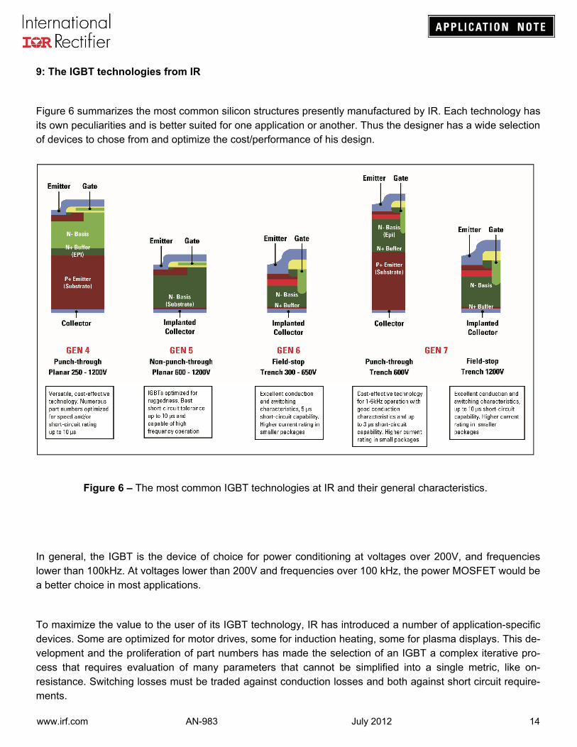
Figure 6 summarizes the most common silicon structures presently manufactured by IR. Each technology has its own peculiarities and is better suited for one application or another. Thus the designer has a wide selection of devices to chose from and optimize the cost/performance of his design.
In general, the IGBT is the device of choice for power conditioning at voltages over 200V, and frequencies lower than 100kHz. At voltages lower than 200V and frequencies over 100 kHz, the power MOSFET would be a better choice in most applications.
To maximize the value to the user of its IGBT technology, IR has introduced a number of application-specific devices. Some are optimized for motor drives, some for induction heating, some for plasma displays. This de-velopment and the proliferation of part numbers has made the selection of an IGBT a complex iterative pro-cess that requires evaluation of many parameters that cannot be simplified into a single metric, like on-resistance. Switching losses must be traded against conduction losses and both against short circuit require-ments.
Figure 6 – The most common IGBT technologies at IR and their general characteristics.
www.irf.com AN-983 July 2012 15
To make this task easier, IR developed a web-tool that suggests a short list of parts that meet the constraints of the application. It provides an estimate of losses and comparative prices. The tool can be found at:
http://mypower.irf.com/IGBT
One convenient way of comparing performance in an application-related environment is the Current vs. Fre-quency curve, pioneered by IR from the very beginning. It shows the output current of a half bridge in the proper thermal environment as the frequency is increased. Figure 7 shows the relative performance of three widely different IGBTs mounted on a 2°C/W heat-sink with a 1°C/W insulator. Ambient is at 55°C and junction temperature is stipulated to be 150°C. Switching voltage is 400V, 50% duty cycle. The die sizes are approxi-mately the same.
This figure is application-related in so far as it takes into account the thermal environment, as well as the elec-trical operating conditions. It is one of the most useful tools to select the optimal IGBT for a specific applica-tion.
Figure 7. This Current vs. Frequency curve compares the performance of three different IGBTs in a hard-switched half-bridge. The IRG7PC35SD is optimized for conduction, the IRGB20B60PD1 for switching, while the IRGP4069D is a general purpose trench device.
www.irf.com AN-983 July 2012 16
The IRG7PC35SD is a high-density trench device specifically targeted for low voltage drop (resonant applica-tions). As it should be expected, its low-frequency current-carrying capability is remarkable.
The IRGB20B50PD1 is a Gen 5 planar device, introduced in the late nineties. It may still be the best device at high frequency, in spite of the fact that its voltage drop is much higher than the trench devices
The IRGP4069D is a general purpose trench device for hard-switching applications.
10. For more information
AN990: Application Characterization of IGBTs
AN978: HV Floating MOS Gate Drivers
AN1057: Heat-sink Characteristics
AN944: Use Gate Charge to Design the Gate Drive Circuit for Power MOSFETs and IGBTs