For the very latest specifications visit www.aeroflex.com Application Note An insight intermodulation distortion measurement methods using the IFR 2026A/B MultiSource Generator. Intermodulation Distortion
Transcript
For the very latest specifications visit www.aeroflex.com
ApplicationNote
An insight intermodulation distortion measurement
methods using the IFR 2026A/B MultiSource Generator.
Intermodulation Distortion
Introduction
Intermodulation distortion (IMD) is a common problem in a vari-
ety of areas of electronics. In RF communications in particular it
represents a difficult challenge to designers who face tougher
requirements on component and sub system linearity. This trend
is driven in part, by an increase in radio spectrum congestion.
This paper aims to identify the mechanisms responsible for gen-
erating intermodulation distortion and to examine some of the
methods which may be used to measure and combat the prob-
lem. The emphasis is largely directed towards radio communica-
tions, yet many of the principles are directly applicable to other
fields of application. Where appropriate, examples of real test
applications are introduced.
What is ‘IMD’?
Intermodulation distortion is the result of two or more signals
interacting in a non linear device to produce additional unwanted
signals. These additional signals (intermodulation products) occur
mainly in devices such as amplifiers and mixers, but to a lesser
extent they also occur in passive devices such as those found in
many transmission systems. For example, RF connectors on
transmission feeds may become corroded over time resulting in
them behaving as non linear diode junctions. The same can apply
at the junction of different metals or where magnetic materials are
used.
Two interacting signals will produce intermodulation products at
the sum and difference of integer multiples of the original fre-
quencies.
For two input signals, the output frequency components can be
expressed as:
mf1±nf2
where, m and n are integers ³1
The order of the intermodulation product is the sum of the inte-
gers m+n. The ‘two tone’ third order components, (2*f1-f2 and
2*f2-f1) are particularly important because unlike 2nd order dis-
tortion, i.e. harmonic distortion at 2*f1 or 2*f2, they can occur at
frequencies close to the desired/interfering signals and so cannot
be easily filtered. Higher order intermodulation products are gen-
erally less important because they have lower amplitudes and are
more widelyspaced. The remaining third order products, 2f1+f2
and 2f2+f1, do not generally present a problem. The distribution
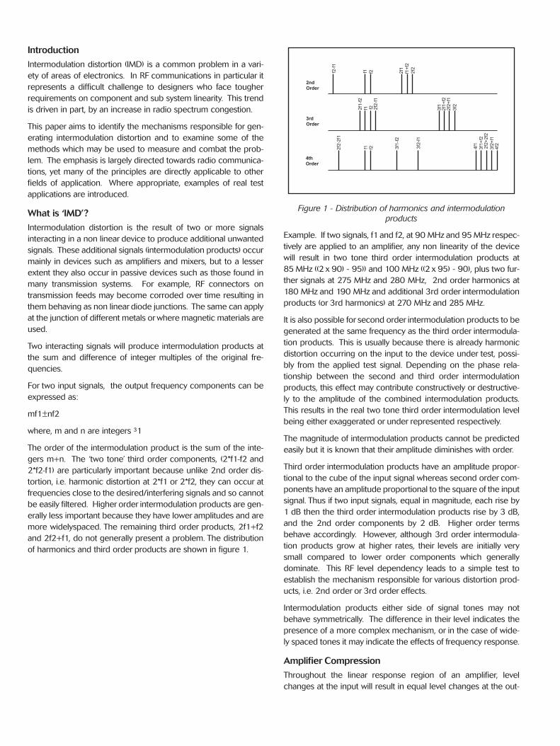
of harmonics and third order products are shown in figure 1.
Figure 1 - Distribution of harmonics and intermodulation
products
Example. If two signals, f1 and f2, at 90 MHz and 95 MHz respec-
tively are applied to an amplifier, any non linearity of the device
will result in two tone third order intermodulation products at
85 MHz ((2 x 90) - 95)) and 100 MHz ((2 x 95) - 90), plus two fur-
ther signals at 275 MHz and 280 MHz, 2nd order harmonics at
180 MHz and 190 MHz and additional 3rd order intermodulation
products (or 3rd harmonics) at 270 MHz and 285 MHz.
It is also possible for second order intermodulation products to be
generated at the same frequency as the third order intermodula-
tion products. This is usually because there is already harmonic
distortion occurring on the input to the device under test, possi-
bly from the applied test signal. Depending on the phase rela-
tionship between the second and third order intermodulation
products, this effect may contribute constructively or destructive-
ly to the amplitude of the combined intermodulation products.
This results in the real two tone third order intermodulation level
being either exaggerated or under represented respectively.
The magnitude of intermodulation products cannot be predicted
easily but it is known that their amplitude diminishes with order.
Third order intermodulation products have an amplitude propor-
tional to the cube of the input signal whereas second order com-
ponents have an amplitude proportional to the square of the input
signal. Thus if two input signals, equal in magnitude, each rise by
1 dB then the third order intermodulation products rise by 3 dB,
and the 2nd order components by 2 dB. Higher order terms
behave accordingly. However, although 3rd order intermodula-
tion products grow at higher rates, their levels are initially very
small compared to lower order components which generally
dominate. This RF level dependency leads to a simple test to
establish the mechanism responsible for various distortion prod-
ucts, i.e. 2nd order or 3rd order effects.
Intermodulation products either side of signal tones may not
behave symmetrically. The difference in their level indicates the
presence of a more complex mechanism, or in the case of wide-
ly spaced tones it may indicate the effects of frequency response.
Amplifier Compression
Throughout the linear response region of an amplifier, level
changes at the input will result in equal level changes at the out-
For the very latest specifications visit www.aeroflex.com
put, assuming a fixed gain. For high input levels the amplifier out-
put is limited by a number of factors, most notably by the magni-
tude of the DC rails. At the point which the amplifier output
becomes non linear with respect to its input, the amplifier is said
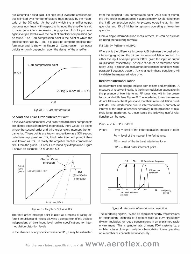
to have gone into compression. A graphical plot of input level
against output level allows the point of amplifier compression can
be found. The 1 dB compression point is the point at which the
amplifier gain falls by 1 dB. It is used to compare amplifier per-
formance and is shown in Figure 2. Compression may occur
quickly or slowly depending upon the design of the amplifier.
Figure 2 - 1 dB compression
Second and Third Order Intercept Point
If the levels of fundamental, 2nd order and 3rd order components
are plotted against input level, theoretically there would be points
where the second order and third order levels intercept the fun-
damental. These points are known respectively as a SOI, second
order intercept point and TOI, third order intercept point, (other-
wise known as IP3). In reality, the amplifier reaches compression
first. From the graph, TOI orSOI are found by extrapolation. Figure
3 shows an example TOI (IP3) and SOI.
Figure 3 - Graph of SOI and TOI
The third order intercept point is used as a means of rating dif-
ferent amplifiers and mixers, allowing a comparison of the devices
independent of their input level, unlike specifications for inter-
modulation distortion levels.
In the absence of any specified value for IP3, it may be estimated
from the specified 1 dB compression point. As a rule of thumb,
the third-order intercept point is approximately 10 dB higher than
the 1 dB compression point for systems operating at high fre-
quencies and 15 dB higher for systems operating at lower fre-
quencies.
From a single intermodulation measurement, IP3 can be estimat-
ed using the following formula:
IP3 (dBm)= P(dBm) + A(dB)/2
Where A is the difference in power (dB) between the desired or
interfering signal, and the third-order intermodulation product. P is
either the input or output power (dBm), given the input or output
values for IP3 respectively. The value of A must be measured accu-
rately using a spectrum analyzer under constant conditions (tem-
perature, frequency, power). Any change in these conditions will
invalidate the measured value of A.
Receiver intermodulation
Receiver front end designs include both mixers and amplifiers. A
measure of receiver linearity is the intermodulation attenuation in
the presence of two interfering RF tones lying within the prese-
lector bandwidth, (see Figure 4). The interfering tones themselves
do not fall inside the IF passband, but their intermodulation prod-
ucts do. The interference due to intermodulation is primarily of
interest at the limits of receiver sensitivity in the presence of rela-
tively large interferers. At these levels the following useful rela-tionship can be used.
Pimp = 2PA + PB - 2PIP3
Where Pimp = level of the intermodulation product in dBm
PA = level of the nearest interfering tone.
PB = level of the furthest interfering tone.
PIP3 = Third order intercept point.
Figure 4. Receiver intermodulation rejection
The interfering signals, FA and FB represent nearby transmissions
on neighboring channels of a system such as FDM (frequency
division multiplex) or rogue transmissions in an unplanned radio
environment. This is symptomatic of many FDM systems i.e. a
mobile radio in close proximity to a base station tower operating
on a number of channels simultaneously.
The frequency spacing of the two tones used in tests is chosen to
be greater than the receivers I.F. bandwidth to ensure that the
measurement is not affected by the selectivity characteristics of
the receiver. The two frequencies must also be chosen to ensure
that their intermodulation products fall inside the receiver IF band-
width. For example AMPS (Advanced Mobile Phone System)
receiver intermodulation tests are performed with interferers
spaced 60 kHz and 120 kHz away from the in channel signal,
which equates to 2 and 4 channels offset respectively. AMPS
radios are also tested with 300 kHz and 600 kHz spacings.
Three Tone IM Distortion
Some devices are operated in conditions where a number of
inputs may be present, in which case testing should be carried
out with multiple outputs.
The effect of intermodulation distortion may differ with the intro-
duction of further interfering signals. With three signals present at
the input of an amplifier or mixer, three sets of IM products are
produced (caused by f1&f2 combining, f1&f3 combining and
f2&f3 combining), this is shown in figure 5. A total of 15 different
third order products may be generated (including 3rd harmonics)
of which 6 are important. For equally spaced tones, 2 of these 6
occur at the same frequency as two of the interfering tones, (C
and D in figure 5 below). The phase relationship between these
intermodulations and the associated interfering signal modifies
their combined level. This in turn results in a change in the level
of the other intermodulation products generated.
A test system assembled for this purpose should allow control of
the phase of each signal relative to a common reference, in order
that the worse case intermodulation distortion products may be
found.
Figure 5. Three tone intermodulation products
For three signals, the worst intermodulation levels are typically
when the phase of the signals are adjusted to give the largest
amount of peak envelope power.
Measuring Intermodulation Distortion Products
The level of intermodulation may be dependent on many vari-
ables such as: the input frequency, amplitude and terminating
impedance. Therefore, any measurement of third order IM dis-
tortion products must be done under constant, controlled condi-
tions.
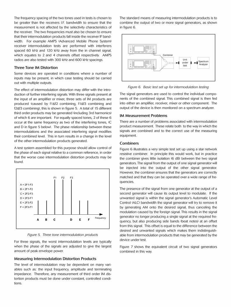
The standard means of measuring intermodulation products is to
combine the output of two or more signal generators, as shown
in figure 6.
Figure 6. Basic test set up for intermodulation testing
The signal generators are used to control the individual compo-
nents of the combined signal. This combined signal is then fed
into either an amplifier, receiver, mixer or other component. The
output of the device is then monitored on a spectrum analyzer.
IM Measurement Problems
There are a number of problems associated with intermodulation
product measurement. These relate both to the way in which the
signals are combined and to the correct use of the measuring
equipment.
Combiners
Figure 6 illustrates a very simple test set up using a star network
resistive combiner. In principle this would work, but in practice
the combiner gives little isolation (6 dB) between the two signal
generators. The signal from the output of one signal generator will
be injected into the output of the other signal generator.
However, the combiner ensures that the generators are correctly
matched and that they can be operated over a wide range of fre-
quencies.
The presence of the signal from one generator at the output of a
second generator will cause its output level to modulate. If the
unwanted signal is within the signal generator’s Automatic Level
Control (ALC) bandwidth the signal generator will try to remove it
by generating AM onto the desired signal, thus canceling the
modulation caused by the foreign signal. This results in the signal
generator no longer producing a single signal at the required fre-
quency, but also producing side bands (beat notes) at an offset
from this signal. This offset is equal to the difference between the
desired and unwanted signals which makes them indistinguish-
able from intermodulation products that may be generated by the
device under test.
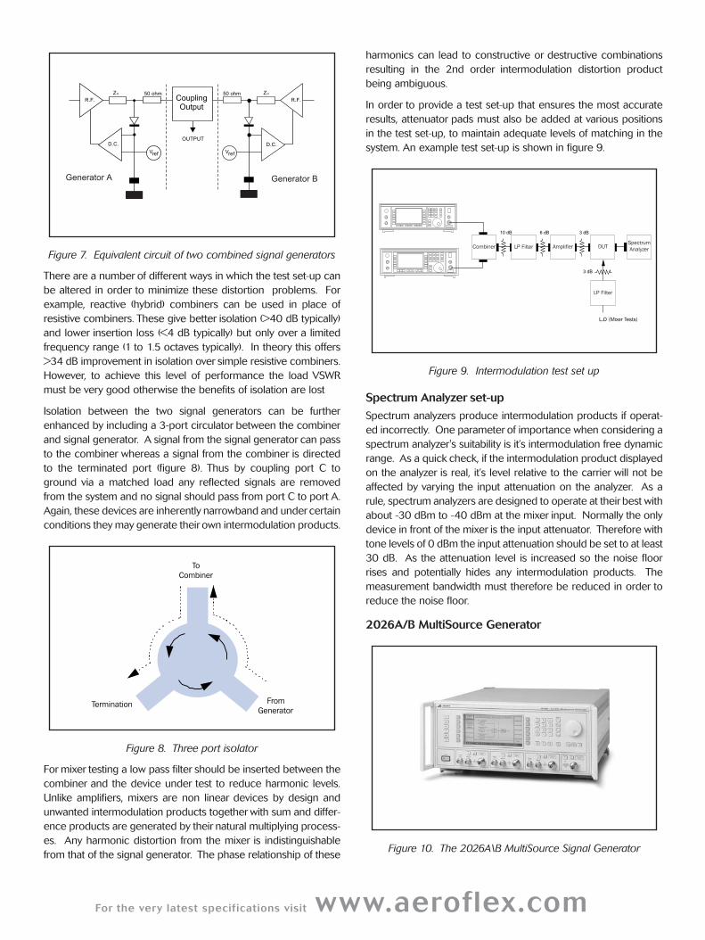
Figure 7 shows the equivalent circuit of two signal generators
combined in this way.
For the very latest specifications visit www.aeroflex.com
Figure 7. Equivalent circuit of two combined signal generators
There are a number of different ways in which the test set-up can
be altered in order to minimize these distortion problems. For
example, reactive (hybrid) combiners can be used in place of
resistive combiners. These give better isolation (>40 dB typically)
and lower insertion loss (<4 dB typically) but only over a limited
frequency range (1 to 1.5 octaves typically). In theory this offers
>34 dB improvement in isolation over simple resistive combiners.
However, to achieve this level of performance the load VSWR
must be very good otherwise the benefits of isolation are lost
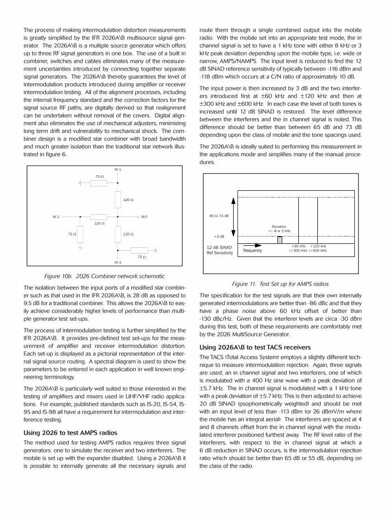
Isolation between the two signal generators can be further
enhanced by including a 3-port circulator between the combiner
and signal generator. A signal from the signal generator can pass
to the combiner whereas a signal from the combiner is directed
to the terminated port (figure 8). Thus by coupling port C to
ground via a matched load any reflected signals are removed
from the system and no signal should pass from port C to port A.
Again, these devices are inherently narrowband and undercertain
conditions they may generate their own intermodulation products.
Figure 8. Three port isolator
For mixer testing a low pass filter should be inserted between the
combiner and the device under test to reduce harmonic levels.
Unlike amplifiers, mixers are non linear devices by design and
unwanted intermodulation products together with sum and differ-
ence products are generated by their natural multiplying process-
es. Any harmonic distortion from the mixer is indistinguishable
from that of the signal generator. The phase relationship of these
harmonics can lead to constructive or destructive combinations
resulting in the 2nd order intermodulation distortion product
being ambiguous.
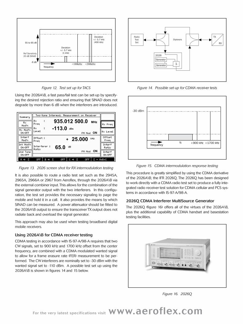
In order to provide a test set-up that ensures the most accurate
results, attenuator pads must also be added at various positions
in the test set-up, to maintain adequate levels of matching in the
system. An example test set-up is shown in figure 9.
Figure 9. Intermodulation test set up
Spectrum Analyzer set-up
Spectrum analyzers produce intermodulation products if operat-
ed incorrectly. One parameter of importance when considering a
spectrum analyzer's suitability is it’s intermodulation free dynamic
range. As a quick check, if the intermodulation product displayed
on the analyzer is real, it’s level relative to the carrier will not be
affected by varying the input attenuation on the analyzer. As a
rule, spectrum analyzers are designed to operate at their best with
about -30 dBm to -40 dBm at the mixer input. Normally the only
device in front of the mixer is the input attenuator. Therefore with
tone levels of 0 dBm the input attenuation should be set to at least
30 dB. As the attenuation level is increased so the noise floor
rises and potentially hides any intermodulation products. The
measurement bandwidth must therefore be reduced in order to
reduce the noise floor.
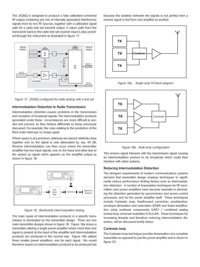
2026A/B MultiSource Generator
Figure 10. The 2026A\B MultiSource Signal Generator
The process of making intermodulation distortion measurements
is greatly simplified by the IFR 2026A\B multisource signal gen-
erator. The 2026A\B is a multiple source generator which offers
up to three RF signal generators in one box. The use of a built in
combiner, switches and cables eliminates many of the measure-
ment uncertainties introduced by connecting together separate
signal generators. The 2026A\B thereby guarantees the level of
intermodulation products introduced during amplifier or receiver
intermodulation testing. All of the alignment processes, including
the internal frequency standard and the correction factors for the
signal source RF paths, are digitally derived so that realignment
can be undertaken without removal of the covers. Digital align-
ment also eliminates the use of mechanical adjusters, minimizing
long term drift and vulnerability to mechanical shock. The com-
biner design is a modified star combiner with broad bandwidth
and much greater isolation than the traditional star network illus-
trated in figure 6.
Figure 10b. 2026 Combiner network schematic
The isolation between the input ports of a modified star combin-
er such as that used in the IFR 2026A\B, is 28 dB as opposed to
9.5 dB for a traditional combiner. This allows the 2026A\B to eas-
ily achieve considerably higher levels of performance than multi-
ple generator test set-ups.
The process of intermodulation testing is further simplified by the
IFR 2026A\B. It provides pre-defined test set-ups for the meas-
urement of amplifier and receiver intermodulation distortion.
Each set-up is displayed as a pictorial representation of the inter-
nal signal source routing. A spectral diagram is used to show the
parameters to be entered in each application in well known engi-
neering terminology.
The 2026A\B is particularly well suited to those interested in the
testing of amplifiers and mixers used in UHF/VHF radio applica-
tions. For example, published standards such as IS-20, IS-54, IS-
95 and IS-98 all have a requirement for intermodulation and inter-
ference testing.
Using 2026 to test AMPS radios
The method used for testing AMPS radios requires three signal
generators: one to simulate the receiver and two interferers. The
mobile is set up with the expander disabled. Using a 2026A\B it
is possible to internally generate all the necessary signals and
route them through a single combined output into the mobile
radio. With the mobile set into an appropriate test mode, the in
channel signal is set to have a 1 kHz tone with either 8 kHz or 3
kHz peak deviation depending upon the mobile type, i.e. wide or
narrow, AMPS/NAMPS. The input level is reduced to find the 12
dB SINAD reference sensitivity of typically between -116 dBm and
-118 dBm which occurs at a C/N ratio of approximately 10 dB.
The input power is then increased by 3 dB and the two interfer-
ers introduced first at ±60 kHz and ±120 kHz and then at
±300 kHz and ±600 kHz. In each case the level of both tones is
increased until 12 dB SINAD is restored. The level difference
between the interferers and the in channel signal is noted. This
difference should be better than between 65 dB and 73 dB
depending upon the class of mobile and the tone spacings used.
The 2026A\B is ideally suited to performing this measurement in
the applications mode and simplifies many of the manual proce-
dures.
Figure 11. Test Set up for AMPS radios
The specification for the test signals are that their own internally
generated intermodulations are better than -86 dBc and that they
have a phase noise above 60 kHz offset of better than
-130 dBc/Hz. Given that the interferer levels are circa -30 dBm
during this test, both of these requirements are comfortably met
by the 2026 MultiSource Generator.
Using 2026A\B to test TACS receivers
The TACS (Total Access System) employs a slightly different tech-
nique to measure intermodulation rejection. Again, three signals
are used; an in channel signal and two interferers, one of which
is modulated with a 400 Hz sine wave with a peak deviation of
±5.7 kHz. The in channel signal is modulated with a 1 kHz tone
with a peak deviation of ±5.7 kHz. This is then adjusted to achieve
20 dB SINAD (psophometrically weighted) and should be met
with an input level of less than -113 dBm (or 26 dBmV/m where
the mobile has an integral aerial). The interferers are spaced at 4
and 8 channels offset from the in channel signal with the modu-
lated interferer positioned furthest away. The RF level ratio of the
interferers, with respect to the in channel signal at which a
6 dB reduction in SINAD occurs, is the intermodulation rejection
ratio which should be better than 65 dB or 55 dB, depending on
the class of the radio.
For the very latest specifications visit www.aeroflex.com
Figure 12. Test set up for TACS
Using the 2026A\B, a fast pass/fail test can be set-up by specify-
ing the desired rejection ratio and ensuring that SINAD does not
degrade by more than 6 dB when the interferers are introduced.
Figure 13. 2026 screen shot for RX intermodulation testing
It is also possible to route a radio test set such as the 2945A,
2965A, 2966A or 2967 from Aeroflex, through the 2026A\B via
the external combiner input. This allows for the combination of the
signal generator output with the two interferers. In this configu-
ration, the test set provides the necessary signaling to page the
mobile and hold it in a call. It also provides the means by which
SINAD can be measured. A power attenuator should be fitted to
the 2026A\B output to ensure the transceiverTX output does not
radiate back and overload the signal generator.
This approach may also be used when testing broadband digital
mobile receivers.
Using 2026A\B for CDMA receiver testing
CDMA testing in accordance with IS-97-A/98-A requires that two
CW signals, set to 900 kHz and 1700 kHz offset from the center
frequency, are combined with a CDMA modulated wanted signal
to allow for a frame erasure rate (FER) measurement to be per-
formed. The CW interferers are nominally set to -30 dBm with the
wanted signal set to -110 dBm. A possible test set up using the
2026A\B is shown in figures 14 and 15 below.
Figure 14. Possible set-up for CDMA receiver tests
Figure 15. CDMA intermodulation response testing
This procedure is greatly simplified by using the CDMA derivative
of the 2026A\B; the IFR 2026Q. The 2026Q has been designed
to work directly with a CDMA radio test set to produce a fully inte-
grated radio receiver test solution for CDMA cellular and PCS sys-
tems in accordance with IS-97-A/98-A.
2026Q CDMA Interferer MultiSource Generator
The 2026Q (figure 16) offers all of the virtues of the 2026A\B,
plus the additional capability of CDMA handset and basestation
testing facilities.
Figure 16. 2026Q
The 2026Q is designed to produce a fully calibrated combined
RF output containing any mix of internally generated interference
signals from its two RF sources, together with a calibrated signal
path for a radio test set transmit output. A return path from the
transceiver back to the radio test set receiver input is also provid-
ed through the instrument as illustrated in figure 17.
Figure 17. 2026Q configured for radio testing with a test set
Intermodulation Distortion In Radio Transmission
Intermodulation distortion causes problems in the transmission
and reception of broadcast signals. The intermodulation products
generated under these circumstances are more difficult to pre-
dict and prevent, as they behave differently to those previously
discussed. For example, the rules relating to the prediction of the
third order intercept no longer apply.
Where space is at a premium, antennas are placed relatively close
together and so the signal is only attenuated by, say, 40 dB.
Reverse intermodulation can then occur where the transmitter
amplifier has two input signals, one on the input and other due to
the picked up signal which appears on the amplifier output as
shown in figure 18.
Figure 18. Backwards intermodulation testing
The main cause of intermodulation products in a specific trans-
mission is dominated by the transmitter design. There are two
main transmitter designs shown in figure 18. Figure 18a shows a
transmitter utilizing a single power amplifier where more than one
signal is present at the input of the amplifier and intermodulation
products are produced in the normal way. Figure 18b utilizes
three smaller power amplifiers, one for each signal. We would
therefore expect no intermodulation products to be produced but
because the isolation between the signals is not perfect then a
reverse signal is fed from one amplifier to another.
Figure 18a. Single amp TX block diagram
Figure 18b. Multi amp configuration
This reverse signal interacts with the transmission signal causing
an intermodulation product to be broadcast which could then
interfere with other systems.
Reducing Intermodulation Distortion
The stringent requirements of modern communications systems
demand that transmitter design employs techniques to signifi-
cantly reduce performance limiting factors such as intermodula-
tion distortion. A number of linearisation techniques for RF trans-
mitters and power amplifiers have become essential in eliminat-
ing the distortion generated by upconversion and power control
processes, and by the power amplifier itself. These techniques
include Cartesian loop, feedforward correction, predistortion,
envelope elimination and restoration (EE&R) and linear amplifica-
tion using nonlinear components (LINC) / combined analog
locked-loop universal modulator (CALLUM). These techniques for
increasing linearity and therefore reducing intermodulation dis-
tortion, will be discussed briefly below.
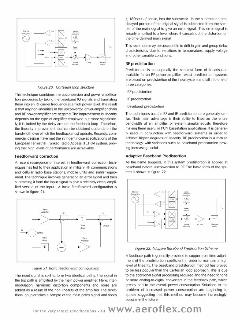
Cartesian loop
The Cartesian loop technique provides linearisation of a complete
transmitter as opposed to just the power amplifier and is shown in
figure 20.
For the very latest specifications visit www.aeroflex.com
Figure 20. Cartesian loop structure
This technique combines the upconversion and power amplifica-
tion processes by taking the baseband IQ signals and translating
them into an RF carrier frequency at a high power level. The result
is that any non-linearities in the upconvertor, driver-amplifier chain
and RF power amplifier are negated. The improvement in linearity
depends on the type of amplifier employed but more significant-
ly, it is limited by the delay around the feedback loop. Therefore,
the linearity improvement that can be obtained depends on the
bandwidth over which the feedback must operate. Recently, com-
mercial designs have met the stringent noise specifications of the
European Terrestrial Trunked Radio Access (TETRA) system, prov-
ing that high levels of performance are achievable.
Feedforward correction
A recent resurgence of interest in feedforward correction tech-
niques has led to their application in military HF communications
and cellular radio base stations, mobile units and similar equip-
ment. The technique involves generating an error signal and then
subtracting it from the input signal to give a relatively clean, ampli-
fied version of the input. A basic feedforward configuration is
shown in figure 21.
Figure 21. Basic feedforward configuration
The input signal is split to form two identical paths. The signal in
the top path is amplified by the main power amplifier. Here, inter-
modulation, harmonic distortion components and noise are
added as a result of the non linearity of the amplifier. The direc-
tional coupler takes a sample of the main paths signal and feeds
it, 180o out of phase, into the subtractor. In the subtractor a time
delayed portion of the original signal is subtracted from the sam-
ple of the main signal to give an error signal. This error signal is
linearly amplified to a level where it cancels out the distortion on
the time delayed main signal.
This technique may be susceptible to drift in gain and group delay
characteristics due to variations in temperature, supply voltage
and other variable conditions.
RF predistortion
Predistortion is conceptually the simplest form of linearisation
available for an RF power amplifier. Most predistortion systems
are based on predistortion of the input system and fall into one of
three categories:
· RF predistortion
· IF predistortion
· Baseband predistortion
The techniques used in RF and IF predistortion are generally sim-
ilar. Their main advantage is their ability to linearize the entire
bandwidth of an amplifier or system simultaneously, therefore
making them useful in PCN basestation applications. It is general-
ly used in conjunction with feedforward systems in order to
achieve higher degrees of linearity. RF predistortion is a mature
technology, with variations such as baseband predistortion prov-
ing increasing useful.
Adaptive Baseband Predistortion
As the name suggests, in this system predistortion is applied at
baseband before upconversion to RF. The basic form of the sys-
tem is shown in figure 22.
Figure 22. Adaptive Baseband Predistortion Scheme
A feedback path is generally provided to support real-time adjust-
ment of the predistortion coefficient in order to maintain a high
level of linearity. The baseband predistortion method has proved
to be less popular than the Cartesian loop approach. This is due
to the additional signal processing required and the need for one
or more analog-to-digital converters in the feedback path, which
greatly add to the overall power consumption. Solutions to the
problem of increased power consumption are beginning to
appear suggesting that this method may become increasingly-
popular in the future.
EE&R (Envelope Elimination and Restoration)
The EE&R technique has the advantage that it can be implement-
ed in a number of different ways. Circuits demonstrating the EE&R
technique implemented as a linear transmitter and as an amplifi-
er linearisation technique are shown in figure 22a and figure 22b
respectively.
Figure 22a. EE&R implemented as a linear transmitter
Figure 22b. EE&R implemented as amplifier linearization
The technique has the theoretical potential to achieve 100% DC
to RF power conversion efficiency at all envelope levels of the
modulation signal. In practice, the efficiency falls short of this,
however, the actual figure may still be in the region of 75%-90%.
Despite these impressive figures, there are a number of practical
limitations to the linearity available from the system. Most signifi-
cantly, where low envelope levels are used, the RF power transis-
tor may cut off introducing significant distortion into the system.
For systems such as p/4-DQPSK systems which involve relatively
modest levels of envelope variation, the technique offers good
potential.
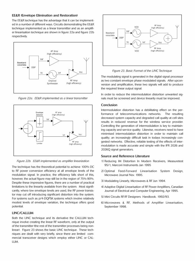
LINC/CALLUM
Both the LINC technique and its derivative the CALLUM tech-
nique involve creating the linear RF waveform, only at the output
of the transmitter (the rest of the transmitter processes being non-
linear). Figure 23 shows the basic LINC technique. These tech-
niques are dealt with very briefly, since there are limited com-
mercial transceiver designs which employ either LINC or CAL-
LUM.
Figure 23. Basic Format of the LINC Technique
The modulating signal is generated in the digital signal processor
as two constant envelope phase modulated signals. After upcon-
version and amplification, these two signals will add to produce
the required linear output signal.
In order to reduce the intermodulation distortion unwanted sig-
nals must be screened and device linearity must be improved.
Conclusion
Intermodulation distortion has a debilitating effect on the per-
formance of telecommunications networks. The resulting
decreased system capacity and degraded call quality at cell sites
results in reduced revenue for the wireless service provider.
Controlling the generation of intermodulation is key to maintain-
ing capacity and service quality. Likewise, receivers need to have
minimised intermodulation distortion in order to maintain call
quality; an increasingly difficult task in todays increasingly con-
gested networks. Effective, reliable testing of the effects of inter-
modulation is made accurate and simple with the IFR 2026 and
2026Q signal generators.
Source and Reference Literature
1] Reducing IM Distortion In Modern Receivers, Measuretest
95/1, Marconi Instruments Jan 1995
2] Optimal Feed-Forward Linearisation System Design,
Microwave Journal Nov. 1995.
3] Modulating Linearly, Microwaves & RF Jun 1994.
4] Adaptive Digital Linearisation of RF Power Amplifiers, Canadian
Journal of Electrical and Computer Engineering, Apr 1995.
5] Mini Circuits RF/IF Designers Handbook. 1992/93.
6] Microwaves & RF, Methods of Amplifier Linearisation,
September 1998.
For the very latest specifications visit www.aeroflex.com
Part No. 46891/846, Issue 2, 05/04
CHINA Beijing
Tel: [+86] (10) 64672716
Fax: [+86] (10) 6467 2821
CHINA Shanghai
Tel: [+86] (21) 6282 8001
Fax: [+86] (21) 62828 8002
FINLAND
Tel: [+358] (9) 2709 5541
Fax: [+358] (9) 804 2441
FRANCE
Tel: [+33] 1 60 79 96 00
Fax: [+33] 1 60 77 69 22
GERMANY
Tel: [+49] 8131 2926-0
Fax: [+49] 8131 2926-130
HONG KONG
Tel: [+852] 2832 7988
Fax: [+852] 2834 5364
INDIA
Tel: [+91] 80 5115 4501
Fax: [+91] 80 5115 4502
KOREA
Tel: [+82] (2) 3424 2719
Fax: [+82] (2) 3424 8620
SCANDINAVIA
Tel: [+45] 9614 0045
Fax: [+45] 9614 0047
SPAIN
Tel: [+34] (91) 640 11 34
Fax: [+34] (91) 640 06 40
UK Burnham
Tel: [+44] (0) 1628 604455
Fax: [+44] (0) 1628 662017
UK Stevenage
Tel: [+44] (0) 1438 742200
Fax: [+44] (0) 1438 727601
Freephone: 0800 282388
USA
Tel: [+1] (316) 522 4981
Fax: [+1] (316) 522 1360
Toll Free: 800 835 2352
w w w . a e r o f l e x . c o m
i n f o - t e s t @ a e r o f l e x . c o m
As we are always seeking to improve our products,
the information in this document gives only a general
indication of the product capacity, performance and
suitability, none of which shall form part of any con-
tract. We reserve the right to make design changes