University of Nebraska - Lincoln DigitalCommons@University of Nebraska - Lincoln Mechanical & Materials Engineering Faculty Publications Mechanical & Materials Engineering, Department of 2014 Arising applications of ferroelectric materials in photovoltaic devices Yongbo Yuan University of Nebraska-Lincoln, [email protected]Zhengguo Xiao University of Nebraska–Lincoln, [email protected]Bin Yang University of Nebraska–Lincoln, [email protected]Jinsong Huang University of Nebraska-Lincoln, [email protected]Follow this and additional works at: hp://digitalcommons.unl.edu/mechengfacpub Part of the Mechanics of Materials Commons , Nanoscience and Nanotechnology Commons , Other Engineering Science and Materials Commons , and the Other Mechanical Engineering Commons is Article is brought to you for free and open access by the Mechanical & Materials Engineering, Department of at DigitalCommons@University of Nebraska - Lincoln. It has been accepted for inclusion in Mechanical & Materials Engineering Faculty Publications by an authorized administrator of DigitalCommons@University of Nebraska - Lincoln. Yuan, Yongbo; Xiao, Zhengguo; Yang, Bin; and Huang, Jinsong, "Arising applications of ferroelectric materials in photovoltaic devices" (2014). Mechanical & Materials Engineering Faculty Publications. 107. hp://digitalcommons.unl.edu/mechengfacpub/107
Transcript
University of Nebraska - LincolnDigitalCommons@University of Nebraska - LincolnMechanical & Materials Engineering FacultyPublications
Mechanical & Materials Engineering, Departmentof
2014
Arising applications of ferroelectric materials inphotovoltaic devicesYongbo YuanUniversity of Nebraska-Lincoln, [email protected]
Follow this and additional works at: http://digitalcommons.unl.edu/mechengfacpub
Part of the Mechanics of Materials Commons, Nanoscience and Nanotechnology Commons,Other Engineering Science and Materials Commons, and the Other Mechanical EngineeringCommons
This Article is brought to you for free and open access by the Mechanical & Materials Engineering, Department of at DigitalCommons@University ofNebraska - Lincoln. It has been accepted for inclusion in Mechanical & Materials Engineering Faculty Publications by an authorized administrator ofDigitalCommons@University of Nebraska - Lincoln.
Yuan, Yongbo; Xiao, Zhengguo; Yang, Bin; and Huang, Jinsong, "Arising applications of ferroelectric materials in photovoltaic devices"(2014). Mechanical & Materials Engineering Faculty Publications. 107.http://digitalcommons.unl.edu/mechengfacpub/107
Arising applications of ferroelectric materials inphotovoltaic devices
Yongbo Yuan,† Zhengguo Xiao,† Bin Yang† and Jinsong Huang†*
The ferroelectric-photovoltaic (FE-PV) device, in which a homogeneous ferroelectric material is used as a
light absorbing layer, has been investigated during the past several decades with numerous ferroelectric
oxides. The FE-PV effect is distinctly different from the typical photovoltaic (PV) effect in semiconductor
p–n junctions in that the polarization electric field is the driving force for the photocurrent in FE-PV
devices. In addition, the anomalous photovoltaic effect, in which the voltage output along the
polarization direction can be significantly larger than the bandgap of the ferroelectric materials, has been
frequently observed in FE-PV devices. However, a big challenge faced by the FE-PV devices is the very
low photocurrent output. The research interest in FE-PV devices has been re-spurred by the recent
discovery of above-bandgap photovoltage in materials with ferroelectric domain walls, electric
switchable diodes and photovoltaic effects, tip-enhanced photovoltaic effects at the nanoscale, and new
low-bandgap ferroelectric materials and device design. In this feature article, we reviewed the advance
in understanding the mechanisms of the ferroelectric photovoltaic effects and recent progress in
improving the photovoltaic device performance, including the emerging approaches of integrating the
ferroelectric materials into organic heterojunction photovoltaic devices for very high efficiency PV devices.
1. Introduction to ferroelectricphotovoltaic devices
Clean and sustainable solar energy is regarded as one of themost reliable and abundant energy sources to replace fossilfuels.1,2 The photovoltaic effect is used to directly harvest solar
energy by converting the incident photons into owing freecharge carriers and thus produce electricity. The photovoltaictechnologies have advanced for more than a century aer thediscovery of the photoelectric effect by Einstein.3,4 However,aer decades of development, the commercialized crystallinesilicon solar panels are still too expensive to compete with fossilenergy.5 In order to reduce the energy harvesting cost, thesecond and third generation photovoltaic cells, such as thinlm amorphous silicon solar cells,6 copper indium galliumselenide solar cells,7 dye-sensitized solar cells,8 cadmiumtelluride solar cells,9 quantum dot solar cells,10 organic solar
Yongbo Yuan received his PhDdegree in condensed matterphysics from Sun Yat-senUniversity (China) in 2009,during which his researchfocused on organic light-emit-ting devices. He is currently apostdoctoral fellow in Prof. Jin-song Huang's research group atthe University of Nebraska-Lincoln. His research interestsinclude organic optoelectronicssuch as solar cells, thin lmtransistors and photodetectors.
Zhengguo Xiao obtained his B.S.at Shandong University ofScience and Technology in 2008,and M.S. at the ChineseAcademy of Science in 2011.Thereaer, he joined Prof. Jin-song Huang's research group inthe Department of Mechanicaland Materials Engineering atthe University of Nebraska-Lincoln at 2011 as a PhDstudent. His current researchfocuses on organic electronicdevices including OPVs, OLED,OFETs, etc.
Department of Mechanical and Materials Engineering, Nebraska Center for Materials
and Nanoscience, University of Nebraska, Lincoln, Nebraska 68588-0656, USA. E-mail:
cells,11 perovskite solar cells,12–14 etc. are under intense studybecause of their potential to dramatically reduce the cost by thelower-cost materials and fabrication. The power conversionefficiency (PCE, h) of a solar cell, dened by the electric energyoutput (Pout) divided by the solar energy (Pin) it absorbs, isexpressed as:
h ¼ Pout/Pin ¼ JscVocFF/Pin (1)
where Jsc is the short circuit current density, Voc is the opencircuit voltage, and FF is the ll factor which is the ratio ofmaximum obtainable power to the product of the Voc and Jsc.
The ferroelectric photovoltaic effect was discovered abouthalf a century ago in a variety of ferroelectric materials withoutcentral symmetry in which a steady photovoltaic response(photovoltage and photocurrent) can be generated along thepolarization direction.15,16 Generally, the ferroelectric photo-voltaic effect originates from the spontaneous electric polari-zation in ferroelectric materials.17,18 An unique characteristic ofFE-PV devices is that the photocurrent direction can beswitched by changing the spontaneous polarization direction ofa FE material with the electric eld. To date, the photovoltaiceffect has been studied in the lithium niobate (LiNbO3)family,19–24 barium titanate (BaTiO3 or referred to as BTO),20 leadzirconate titanate (Pb(ZrTi)O3 or PZT) family,25–28 and bismuthferrite (BiFeO3 or BFO) family.29–32
Among the next generation photovoltaic technologies, theferroelectric photovoltaic effect is completely different from thetraditional p–n junction photovoltaic effect as shown in Fig. 1aand b. In traditional p–n junction solar cells (Fig. 1a), theabsorbed photons can pump the electrons from the valenceband of a light absorbing semiconductor material to itsconduction band, with holes le in the valence band. Thephotogenerated electrons and holes are quickly separated bythe built-in electric eld inside the p–n junction and collectedby the respective electrodes.3 Theoretically, the magnitude ofVoc in p–n junction solar cells is determined by the quasi-Fermienergy difference of photogenerated electrons and holes whichis limited by the bandgap of the light absorbing semi-conductors.3 Nevertheless, for the FE-PV devices (Fig. 1b), it is
experimentally observed that the output photovoltage isproportional to the magnitude of electric polarization andelectrode spacing.17,18,30 As a result, a unique and importantcharacteristic of the FE-PV devices is the anomalous photovol-taic (APV) effect, i.e. the output Voc can be a few orders ofmagnitude larger than the bandgap of the FE mate-rials.20,21,30,33,34 The photovoltage is as large as over 104 volts insome cases, e.g. in LiNbO3 bulk crystals.33 This unique FE-PVdevice working mechanism provides another viable route toconvert light into electric energy.
However, long aer its discovery, the FE-PV effect hasremained an academic curiosity rather than having any realisticapplication because of the very low energy conversion efficiencyachieved in regular FE-PV devices. The PCE of FE-PV devicesbased on the pure APV effect had not exceeded 0.1% under 1sun illumination over half a century, mainly due to very smalloutput photocurrent densities in the order of �nA cm�2.29,35–37
The situation has not changed until recent advance in muchbetter engineered ferroelectric materials,30,36 new photocurrentextraction techniques,35,38,39 and particularly the hybridizationof FE-PV devices with traditional p–n junction photovoltaicswhich have yielded comparable or superior device perfor-mances to regular p–n junction devices.40,41
In this feature article, we rst review the advance inunderstanding the mechanism of FE-PV devices, especiallythe origin of the abnormally large photovoltage, as well as thefactors that determine the photocurrent. Then, the recentprogress in enhancing the efficiency of FE-PV devices is dis-cussed which addresses the issues of the absent and/or weakvisible light absorption and low conductivity of commonferroelectric materials. And nally, the most recent advancein the application of ferroelectric materials in high efficiencyorganic photovoltaic (OPV) devices is highlighted. In addi-tion to photovoltaic devices, large bandgap ferroelectricsemiconductors (e.g. PZT and BaTiO3) have also been used toseparate the photogenerated charge pairs in other solarenergy conversion devices, such as photoelectrochemicalcells, which can be found in review papers by Tiwari et al. andwill not be reviewed here.42–45
Bin Yang has been a PhDstudent in Prof. Jinsong Huang'sresearch group in the Depart-ment of Mechanical and Mate-rials Engineering at theUniversity of Nebraska-Lincolnsince 2010. He obtained aB.S. in 2007 and a M.S. in2010 at Hunan University(China). His current researchfocuses on organic optoelec-tronic electronics.
Jinsong Huang received his PhDdegree in Material Science andEngineering from the Universityof California-Los Angeles in2007. Aer working in AgiltronInc. as a research scientist fortwo years, he joined the Univer-sity of Nebraska-Lincoln (UNL)as an assistant professor inthe Department of MechanicalEngineering and NebraskaCenter for Materials and Nano-science. His current research
interests include solution processed electronic materials forapplications in sensing, energy and consumer electronics.
2. Advance in the understanding ofthe ferroelectric photovoltaicmechanism and enhancedperformance2.1 Origin of the large photovoltage in FE-PV devices
It has been controversial on the origin of the APV effect in theferroelectric materials. The typical FE-PV devices with vertical orlateral congurations are illustrated in Fig. 2. The photovoltagehas been shown to be dependent on many factors such as thedistance between the two opposite electrodes,28,46 light inten-sity,47 electrical conductivity33 remnant polarization of theferroelectric crystals/lms,48 crystallographic orientation,49
dimension/size of the crystals,46,50 domain walls30 and theferroelectric/electrode interface.37 In order to explain the ultra-high photovoltage output, several models have been proposedin early years, including the shi current model and thenonlinear dielectric model.51 The common characteristic ofthese theories is that the photovoltage is generated in the bulkof the ferroelectric crystals, hence named as the bulk photo-voltage effect. A recent theory gives an alternative explanationon the origin of the APV effect using a series of domain walls intandem with each other outputting a small photovoltage.30
Other effects related to the ferroelectric/electrode interface, e.g.Schottky effect and screening effect,52–55 are also believed togenerate or inuence the photovoltage output in ferroelectricthin lms. These theories are related to the domain wall inter-face or the FE/electrode interface.
2.1.1 Bulk photovoltaic effect. According to the frequentlycited shi current model, the ferroelectric materials act as a sortof “current-source”.21,33,34,56 The formation of a steady current ( Js)
under illumination is related to the noncentrosymmetric natureof the ferroelectric crystal.1–5,8 In the noncentrosymmetriccrystal, the transition probability of an electron jump from thestate with a momentum of k to the state with a momentum of k0
may be different with the corresponding probability of thereverse process, which causes an asymmetric momentumdistribution of the photogenerated charge carriers and thus asteady photocurrent.17 The total current through the ferroelec-tric materials ( J) can be described as:
J ¼ Js + (sd + sph)E (2)
where sd and sph are the dark conductivity and photoconduc-tivity of the ferroelectric materials, respectively, and E ¼ V/d isthe internal electric eld, depending on the applied voltage (V)and the distance (d) between two electrodes. The FE-PV devicescan be deemed as the current source due to the very low darkconductivity and photoconductivity50 of most ferroelectricmaterials and the large distance between the electrodes.28 TheVoc, corresponding to the condition of J¼ 0, can be described as:
Voc ¼ Ed ¼ Js
sd þ sph
d (3)
The shi current model predicts a larger Voc under strongerlight intensity Iop because it gives a large Js. Voc is expected toincrease linearly with Iop (or Js) if the total conductivity (sd + sph)is insensitive to light intensity. This occurs in a situation wheresph is signicantly lower than sd in the studied light intensityrange. A good example for this case is the FE-PV effect in theLiNbO3 : Fe crystal, in which the Voc increased linearly to 103 to104 V with the light intensity in a range of 0.01–1 W cm�2.33 Onthe other hand, if the sph is much larger than sd in the studiedlight intensity range, a constant Voc is expected since both Js andphotoconductivity sph are correlated with light intensity. Anexample for this case is that a saturated photovoltage wasobserved in the iron-doped potassium niobate (KNbO3 : Fe)crystal. Since KNbO3 : Fe and LiNbO3 : Fe have a similar crystalstructure, the difference in themagnitude of sph is related to themuch longer lifetime of the photogenerated charges inKNbO3 : Fe.22,33
In the nonlinear dielectric model, the large observed pho-tovoltage output is caused by the nonlinear response of thepolarization density to the electric eld of the incident light,which led to an effective DC electric eld throughout theferroelectric materials.51
Fig. 2 FE-PV device architectures: (a) vertical and (b) lateral, in which alarge photovoltage proportional to the electrode spacing can bemeasured along the polarization direction (P).
Fig. 1 The working principle of (a) p–n junction solar cells and (b) FE-PV devices.
2.1.2 Domain wall theory. Recently, Yang et al. studied theAPV effect on the BFO lm with ordered domain strips andlateral device conguration (Fig. 3). They observed that thephotovoltage in the BiFeO3 lm increased linearly with the totalnumber of domain walls along the net polarization direction(perpendicular to the domain walls, Fig. 3a and c).30 Thephotovoltaic effect vanished along the direction perpendicularto the net polarization direction (Fig. 3b and d). The intrinsicpotential drop at domain walls (�10 mV), arising from thecomponent of the polarization perpendicular to the domainwall, induces a huge electric eld of �5 � 106 V m�1 in thenarrow domain wall, which was suggested to be the drivingforce for the dissociation of the photogenerated exciton. Theilluminated domain walls act as nanoscale photovoltagegenerators connected in series, wherein the generated photo-current is continuous and the photogenerated voltage accu-mulates along the net polarization direction. This proposedmechanism is analogous to the concept of tandem solar cells,where the output voltage is the sum of the photovoltage of eachsub-cell. Nevertheless, it was noticed in another publicationthat the domain wall is also considered as a current source, andthe total Voc was determined by the Jsc, the conductivity of the FElm under illumination and the distance between the elec-trodes (eqn (3)).57 This explanation attributed the APV effect tothe exciton generated inside the domain wall and suggestedthat the bulk photovoltaic effect was ignorable due to a quickrecombination of excitons generated outside the domain wall,which is apparently different from those previously repor-ted.21,33,34,51,56 In contrast, it was suggested by Alexe et al. that therecombination of the excitons in the bulk of the BFO domain isnot as quick as expected.38 The authors investigated the BFOsingle crystal with a photoelectric atomic force microscopy(Ph-AFM) system combining with piezoresponse atomic forcemicroscopy (PFM), where both the polarization direction andphotocurrent can be mapped with the same scanningconducting tip. A similar large photocurrent in the regionsinside or outside the domain wall was observed, indicating aweak recombination of the photogenerated carriers in the bulk
of the domains. Later the lifetime of photogenerated charges inbulk BFO was measured to be as long as 75 ms which iscomparable with that near the domain wall.58
There are other facts that cannot be explained solely by thedomain wall theory and that bulk photovoltaic effect theorycannot be excluded. According to the domain wall model, thephotocurrent should be independent of the light polarizationdirections due to the intrinsic potential drop at the domain wallinduced by the polarization charges. However, the dependenceof the photovoltaic current on the polarization direction of theincident light in BFO has been frequently observed,29,31 indi-cating that the origin of the photovoltaic effect in ferroelectricsis more complex than expected. A rst-principle calculationbased on the bulk photovoltaic effect tried to reconcile thecontradictory observations in the BFO devices.59 It wasexplained that the vanished photocurrent along the directionparallel to the striped domain wall in Yang's experiment ismainly attributed to the unique geometry of the stripeddomains, where the bulk photovoltaic effect in each domainwas cancelled by the adjacent domains. It was also pointed outthat the large observed photovoltage in Yang's experimentshould be attributed to the domain wall effect because it formeda photocurrent in the opposite direction with that of the bulkeffect. This study also indicates that the photocurrent due to thedomain wall effect was partially cancelled by the bulk effect. Anenhanced PCE is hence expected if the photovoltaic currentscaused by the bulk photovoltaic effect and domain wall effectcan be designed to be in a same direction.59
2.1.3 Schottky-junction effect. When the ferroelectricsemiconductors form Schottky contacts with metal electrodes,there is photocurrent under illumination driven by the localelectrical eld which is caused by the band bending near theelectrodes. The generated photocurrent is largely determined bythe Schottky barrier height and the depletion region depth.60
The magnitude of the photovoltage caused by the Schottkycontact is still limited to the bandgap of the ferroelectricsemiconductor materials. The photovoltage caused by theSchottky-junction effect was ignored in the early stage of studies
Fig. 3 Schematics of the FE-OPV device with (a) a perpendicular domain wall and (b) a parallel domain wall as demonstrated by Yang et al.30 Thecorresponding photocurrent–voltage curves for the devices in (a) and (b) are shown in (c) and (d), respectively.
because it is much less than the anomalous photovoltage inbulk ferroelectric crystals. This effect becomes more evident inthin lm FE-PV devices because of the small photovoltageoutput in these devices.52,53 Generally, this additional photo-current contribution is absent in the FE-PV devices with thesame electrode contacts, because the photovoltage from the twoSchottky-junctions possess opposite polarization and thuscancel each other. However, this component may play animportant role in the FE-PV device with a vertical structurewhere different electrodes are easier to be implemented.37,61–65
The Schottky-junction effect is independent of the polarizationdirections of the ferroelectric materials, which was used todistinguish the contributions of the Schottky barrier and bulkphotovoltaic effects.66 However, there are situations where thephotovoltage of the Schottky-junction FE-PV devices switchtogether with the ip of spontaneous polarization by theapplied electric bias, which oen originates from some artifacteffects. For example, in reported ferroelectric diodes with avertical structure of gold (Au)/BFO/Au, a rectied dark currentand photovoltage with good switch capability (between about +1V and�1 V) were observed.29,62 It was originally thought that theswitchable photovoltage was caused by the bulk photovoltaiceffect in the BFO lm, but a continued study by the same grouprevealed that the BFO/Au contacts switched between Schottky-contact and Ohmic-contact during the poling process due to theelectromigration of the oxygen vacancies, whereas the photo-voltaic effect was not switched when the oxygen vacancymigration was frozen at cryogenic-temperature.62
2.1.4 Depolarization eld model. In polarized ferroelectriclms, there are high densities of polarization charges on thesurface, which can induce a huge electric eld inside theferroelectric layer if they are not screened. For the BFO with aremnant polarization of 26 mC cm�2, the induced electric eldby the unscreened polarization charges can be as large as 3 �104 V mm�1.67 When ferroelectric thin lms are in contact withmetal or semiconductors, the surface charge caused by theremnant polarization will be imperfectly screened by the freecharges in the metal or semiconductors. Usually the screeningof the surface charge is incomplete because the center of gravityof the polarization charge and the free compensation charge arenot coincident, which results in an electrical eld throughoutthe ferroelectric lm named as the depolarization eld.68–70 Thisdepolarization eld can be large, e.g. the depolarization eld inthe 10–30 nm BTO lm sandwiched between SrRuO3 electrodeswas estimated to be 25–50 V mm�1.71 It is suggested that thedepolarization eld may be the dominating driving force for theseparation of photogenerated charge carrier-pairs. It was alsosuggested that the anomalous photovoltage should be closelyrelated to the degree of screening of the spontaneous polari-zation.35,72–74 The screening charge distribution depends onboth the properties of ferroelectric materials and the metal orsemiconductor, such as the remnant polarization, the freecharge density and the dielectric constant. Meanwhile theimpact of the incomplete screening on the depolarization elddepends on the thickness of the ferroelectric layer: a smallerthickness of the ferroelectric layer results in a larger depolar-ization eld.46,68–70 In general, semiconductors in contact with
ferroelectrics lead to a larger depolarization eld than metalbecause of a weaker screening effect caused by their lower freecharge densities and larger dielectric constants.
Recently, Dong et al. used aluminum-doped zinc oxide(Al : ZnO) as an electrode material, in which a larger photo-voltage by about 0.25 V was found as compared to that ofdevices with the Au electrode. A larger depolarization electriceld was suggested as one of the reasons for the increasedphotovoltage.74 Chen et al. studied the FE-PV effect of a 400 nm-thick PZT lm sandwiched between two transparent indium tinoxide (ITO) layers. The ITO lms were used as electrodesbecause a large depolarization eld was expected. Theyobserved a gradually decreased photovoltage output from 0.4 Vto 0.1 V and attributed it to a reduced depolarization eld in thePZT lm caused by different remnant polarizations.73,74 Thetunable screening effect provides opportunities to verify if thedepolarization eld has a critical contribution to the APV.However, the relationship of the depolarization eld and thephotovoltage output in the previous reports were not clearlyrevealed due to the presence of some other mechanism such asdifferent built-in potential or changed remnant polarization.73,74
On the other hand, it has been observed that the inuence ofthe depolarization eld on the photocurrent is stronger than onthe photovoltage, where tens of times improvement in thephotocurrent was reported experimentally and computation-ally, as will be discussed below.35,72
Since the depolarization eld is inversely proportional to thedistance between the two electrodes, the depolarization eldcan play a role in the photovoltaic response only when theferroelectric lms are thin (<100 nm) but it will be too low toaccount for the photovoltaic effect in bulk ferroelectric crystals(>100 mm).46,68–70
2.2 Factors determining the photocurrent in FE-PV devices
In contrast to the huge photovoltage output, the photocurrentsof the FE-PV device are quite low, usually in the order of nAcm�2.17 The photocurrent of the FE-PV device is determined bythe light absorption process, dissociation efficiency of theexcitons, lifetime of the photogenerated nonequilibriumcharges and the charge carrier mobility. The photocurrentunder a certain wavelength light illumination was described byan empirical equation called Glass law: Js¼ akIop, where a is theabsorption coefficient, k is the Glass coefficient which is relatedto the charge generation and collection efficiency and Iop is thelight intensity as mentioned above.21
2.2.1 Optical bandgap and absorption coefficient. Similarto any type of photovoltaic device, the ferroelectric materialsshould be able to absorb as much sun light as possible to have areasonably large photocurrent, which requires the ferroelectricmaterials to have a low bandgap and large absorption coeffi-cient. Most of the commonly used ferroelectric materials, suchas LiNbO3, BaTiO3, and PZT crystal, have a bandgap larger than 3eV, thus can only harvest sunlight in the UV range. However, thetotal energy of the light with a wavelength less than 400 nmconstitutes only about 3.5% of solar energy. Hence it is crucial todevelop ferroelectric materials with a reduced bandgap. Recently
BFO has attracted intensive research interest for optoelectronicsapplication because of its lower bandgap.29,31,36,55,62,74–80 Thebandgaps of its rhombohedral single crystal, rhombohedralpolycrystalline,75,76 and pseudocubic perovskite structure29 are2.2 eV, 2.31–2.63 eV and 2.7 eV, respectively. So theoretically itcan absorb visible light up to 560 nm, allowing about 25% of thesolar energy to be absorbed. The optical absorption spectrumcan also be adjusted by manipulating the ferroelectric materialcompositions through chemical doping or alloying. Forexample, in the LiNbO3 or KNbO3 crystals, Fe-doping extends theabsorption edge to the region of 400–500 nm, corresponding tothe excitation of electrons from Fe2+ ions to the conduction bandof the crystals.81 In BaTiO3, Fe-doping can extend the absorptionedge to around 647 nm.82Recently, ferroelectric bismuth titanateBi4Ti3O12 (BiT) with a wide bandgap tenability of 1 eV has beendemonstrated by alloying it with Mott insulator LaCoO3 (LCO). Aunique unit cell structure, featured by an alternating arrange-ment of the BiT and LCO layers, has been demonstrated tosystematically tune the optical bandgap of BiT from �3.6 eV to�2.7 eV with its strong ferroelectric property uninuenced.83 Inaddition, one general type of defects in ferroelectric oxide is theoxygen vacancy which can broaden the absorption spectrum ifthere is a large density. For example, the oxygen vacancies in theBFO lm can extend the absorption spectrum to 560–650 nm.77
The density of the oxygen vacancies can be controlled by thermalannealing, while the spatial distribution of the oxygen vacanciescan be shied by electrical pulses.62,84–86 Interestingly, the lightabsorption was also reported to be enhanced by utilizing theinternal photoelectric effect at the metal electrode, where theelectrons excited from the metal electrode to the PZT lmrequire photons with energy less than the bandgap of PZT. Thiscomponent was also found to contribute to the measuredphotocurrent.60
In addition to the large optical bandgap, the small absorptioncoefficient of the ferroelectric materials is another issue limitingthe photocurrent. A strong absorption allows a thinner lm to beused which is benecial for charge collection. Most oxides havevery low absorption coefficients in the visible range. Theabsorption coefficient of PZT and BFO families (104 to 105 cm�1
at around 400 nm) is about three to fourmagnitudes higher thanthat of LiNbO3 and BaTiO3 materials (10–100 cm�1 at around400 nm),80,84,87,88 which enables a high light absorption in PZTand BFO lms with a thickness of hundreds of nanometers. Theoptimized sample thickness for a maximized photocurrent is atradeoff between light absorption and charge collection.
2.2.2 Exciton dissociation efficiency. The electron–holepairs (or excitons) generated by incident photons with energyabove the bandgap need to be dissociated efficiently to generatephotocurrent. The binding energy of the excitons is inverselyproportional to the dielectric constant of an active material.Fortunately, the dielectric constant of most ferroelectric mate-rials (102 to 103) is much larger than that of organic and inor-ganic semiconductors (3–13), hence a small binding energybetween holes and electrons is expected. According to the Glassmodel, the separation of the electrons and holes is driven by thenoncentrosymmetric potential well in the unit cells.11,22 Theexcited electrons generally shi along the polarization direction
by only several angstroms before they decay, explaining the verysmall photocurrent in FE-PV devices.33 From this point of view, itis necessary to increase the noncentrosymmetry of the crystal bydeveloping new ferroelectric materials for improved photocur-rents.24,59,89,90 It is known that changing the chemical composi-tion of ferroelectric materials can signicantly change theircrystal structures and thus the degree of noncentrosymmetry,which can affect the photovoltaic response.91–93 For example, inthe PZT ceramics, when the Zr/Ti atomic ratio varies from 48/53to 54/46, the crystal structure changes from tetragonal torhombohedral, where the latter shows stronger crystallographicasymmetry. Therefore in the lanthanum-doped PZT (PLZT)ceramics, the photocurrent was observed to increase by six timeswhen the dopant loading was reduced from 6% to 4%.91
2.2.3 Charge collection efficiency. The next step aerexciton dissociation is the collection of free charges. Thecharge collection efficiency is determined by the carrier life-time, the carrier mobility and the electric eld. The lifetime ofthe photogenerated nonthermalized charges in ferroelectricmaterials was thought to be in the picosecond scale,17 whilethe recombination lifetime was measured to be sub-micro-seconds to tens of microseconds.58,94 Reducing the thicknessof the low conductive ferroelectric lm can lead to increasedcharge collection efficiencies, e.g. Ichiki et al. compared thephotovoltaic effects of the PLZT bulk crystal (with a thicknessof 2.4 mm) and PLZT thin lm (with a thickness of 4 mm) andfound an improvement of over 100 times in the photocur-rent.28 However, the photovoltage was observed to decreasesimultaneously when the thickness was reduced. Anotherapparent method to increase the charge collection efficiency isto increase the collecting electric eld. For example, in theBFO based device, Zang et al. replaced the ITO electrode withnitric acid (HNO3) treated graphene and observed a muchincreased photocurrent of 2.8 mA cm�2, which was attributed
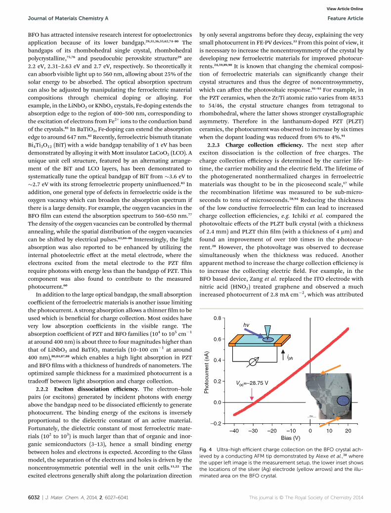
Fig. 4 Ultra-high efficient charge collection on the BFO crystal ach-ieved by a conducting AFM tip demonstrated by Alexe et al.,38 wherethe upper left image is the measurement setup, the lower inset showsthe locations of the silver (Ag) electrode (yellow arrows) and the illu-minated area on the BFO crystal.
to the extended depletion region throughout the entire ferro-electric layer by the formation of metal–intrinsic semi-conductor–metal (MIM) structure.78 It should be noticed thatrecently Alexe et al. observed a tip-enhanced photovoltaiceffect in the BFO lm, where the photogenerated carriers inthe bulk of the BFO lm were collected very efficiently by theAFM tips (Fig. 4).38 The nonuniform local electric eld due to aparticular geometry of the tip contributed to the very highphotocurrent density of 10–100 A cm�2 which is eight orders ofmagnitude higher than that in devices with parallel electrodes.This result might enable promising large-area ferroelectricphotovoltaic devices with much improved photocurrent byusing nano-tip arrays as the electrodes.
There has been an interesting idea on utilization of theincreased depolarization eld for enhanced charge collectionefficiency. Since the depolarizing eld is strongly inuencedby the screening condition at the ferroelectric/electrode
interface and lm thickness,46,68–71 an increased excitondissociation as well as charge collection is expected byreducing the screening of the spontaneous polarization andthe lm thickness. Qin et al. did a theoretical calculationwhich suggested that the photocurrent in PLZT could beincreased by tens of times by (1) replacing the metal electrodewith semiconductors (reduced screening effect) and (2)reducing the PLZT thickness.35 The maximum internal powerconversion efficiency was calculated to be as high as 18.7%for an 8 nm thick PLZT lm. However, when an ultra-thin FElayer is used, one accompanying problem is that the lightabsorption will be severely reduced. In the experimental part,Chen et al. studied the anomalous photovoltaic effect in thedevice with a structure of Au/polycrystalline BFO/Au andfound that the photocurrent output was increased 24 timeswhen the Au electrode was replaced by ITO, which wasattributed to the increased depolarizing eld.72
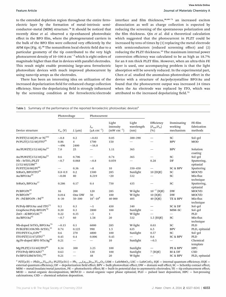
Table 1 Summary of the performance of the reported ferroelectric photovoltaic devicesa
Device structure
Photovoltage Photocurrent
Efficiency(Pout/Pin)(%)
Dominatingworkingmechanism
FE-lmfabricationmethodsVoc (V) L (mm)
Isc(mA cm�2)
Lightintensity(mW cm�2)
Lightwavelength(nm)
Pt/PZT(52/48)/Pt or Ni102 �0.8 0.2 �0.03 0.05 300–390 — SC Sol–gelPt/PLZT(3/52/48)/ITO28 0.86 4 1700 150 — — BPV MOD
Another unique property of the FE-PV devices is that theirphotovoltaic output is switchable with the polarization.Generally, the photovoltages in the opposite polingdirection should be symmetric, i.e. |V+poling| ¼ |V�poling|, butthe symmetry can be lost due to other effects such as anadditional built-in electric eld coming from the work functiondifference of the electrodes and graded composition in FElms.36,37,61,62,66 On the other hand, the magnitude of the pho-tovoltage aer multiple switching tends to systematicallydecrease due to ferroelectric fatigue. The ferroelectric fatigue isa common behavior in ferroelectric materials which can resultfrom (1) charge trapping at the domain wall or near the elec-trode which screens the polarization eld;61,95–98 (2) theformation of defects, such as oxygen vacancies, at the FE/electrode interface which pins the domain boundaries andhinders their movements under an applied electric eld;98 (3)the formation of cracks or de-adhesion of the lm from thesubstrate from due to the residual tensile or compressivestress.99 Recently, Guo et al. demonstrated a novel non-volatilememory array based on the photovoltaic effect in BFO, wherethe photovoltaic output (Voc or Jsc) was used as the read-outsignal. The photovoltage output can be robustly switchedbetween 0.11 V and �0.23 V for up to 108 cycles.100
In ferroelectric materials, the rising time of the photocurrentwas reported to be about 10�5 s.58 The response speed of thephotovoltage is pretty slow. The saturation of the photovoltageoutput under a continuous illumination takes tens to hundredsof seconds,94 which is several orders of magnitude slower thanthat in the conventional PV effect. The slow response time isthought to be related to the very small photoconductivity.81,101 Ingeneral, larger photocurrents lead to faster photovoltaicresponse. Hence it is not surprising that the response time isalso dependent on the light intensity and wavelength.102
To date, numerous inorganic FE-PV devices have beenstudied. The device structures, photovoltaic performance andthe dominating working mechanisms of the related devices aresummarised in Table 1.
3. Recent progress in the integrationof ferroelectric materials in organicphotovoltaic devices
Although there is no demonstration of efficient photovoltaicdevices based on the FE-PV effect yet, there has been signicantprogress recently in the integration of ferroelectric materials intraditional p–n junction photovoltaic devices to overcome thechallenges in these traditional devices. Here the working prin-ciples and challenges in organic photovoltaic devices areintroduced and approaches to address them are reviewed.
3.1 Introduction to organic solar cells and the challenge inefficiency enhancement
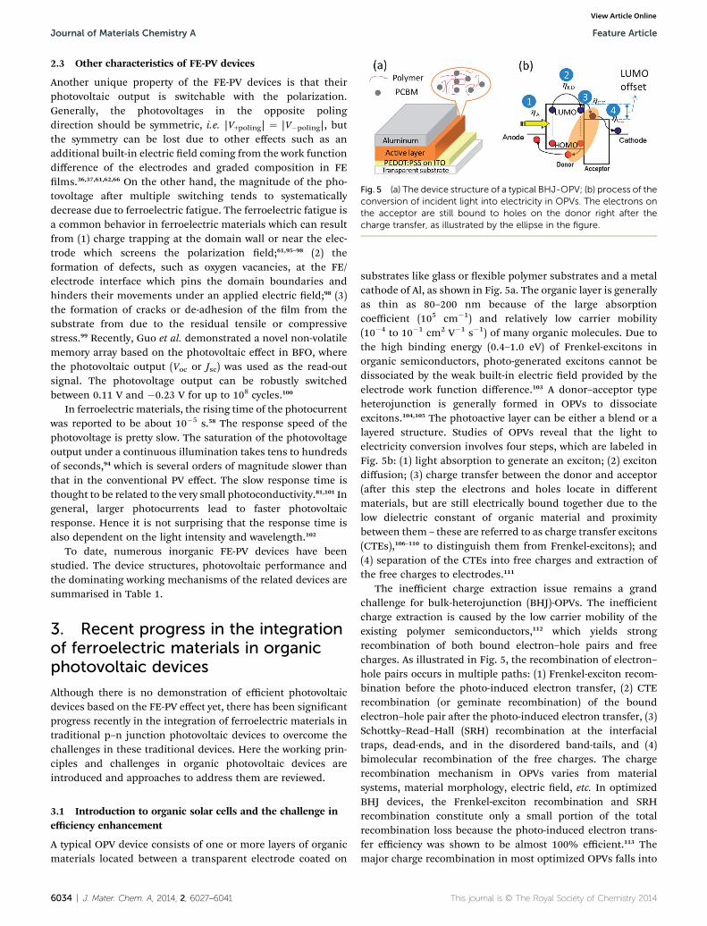
A typical OPV device consists of one or more layers of organicmaterials located between a transparent electrode coated on
substrates like glass or exible polymer substrates and a metalcathode of Al, as shown in Fig. 5a. The organic layer is generallyas thin as 80–200 nm because of the large absorptioncoefficient (105 cm�1) and relatively low carrier mobility(10�4 to 10�1 cm2 V�1 s�1) of many organic molecules. Due tothe high binding energy (0.4–1.0 eV) of Frenkel-excitons inorganic semiconductors, photo-generated excitons cannot bedissociated by the weak built-in electric eld provided by theelectrode work function difference.103 A donor–acceptor typeheterojunction is generally formed in OPVs to dissociateexcitons.104,105 The photoactive layer can be either a blend or alayered structure. Studies of OPVs reveal that the light toelectricity conversion involves four steps, which are labeled inFig. 5b: (1) light absorption to generate an exciton; (2) excitondiffusion; (3) charge transfer between the donor and acceptor(aer this step the electrons and holes locate in differentmaterials, but are still electrically bound together due to thelow dielectric constant of organic material and proximitybetween them – these are referred to as charge transfer excitons(CTEs),106–110 to distinguish them from Frenkel-excitons); and(4) separation of the CTEs into free charges and extraction ofthe free charges to electrodes.111
The inefficient charge extraction issue remains a grandchallenge for bulk-heterojunction (BHJ)-OPVs. The inefficientcharge extraction is caused by the low carrier mobility of theexisting polymer semiconductors,112 which yields strongrecombination of both bound electron–hole pairs and freecharges. As illustrated in Fig. 5, the recombination of electron–hole pairs occurs in multiple paths: (1) Frenkel-exciton recom-bination before the photo-induced electron transfer, (2) CTErecombination (or geminate recombination) of the boundelectron–hole pair aer the photo-induced electron transfer, (3)Schottky–Read–Hall (SRH) recombination at the interfacialtraps, dead-ends, and in the disordered band-tails, and (4)bimolecular recombination of the free charges. The chargerecombination mechanism in OPVs varies from materialsystems, material morphology, electric eld, etc. In optimizedBHJ devices, the Frenkel-exciton recombination and SRHrecombination constitute only a small portion of the totalrecombination loss because the photo-induced electron trans-fer efficiency was shown to be almost 100% efficient.113 Themajor charge recombination in most optimized OPVs falls into
Fig. 5 (a) The device structure of a typical BHJ-OPV; (b) process of theconversion of incident light into electricity in OPVs. The electrons onthe acceptor are still bound to holes on the donor right after thecharge transfer, as illustrated by the ellipse in the figure.
two categories:112,114 geminate recombination113,115–118 andbimolecular recombination,117,119–123 although the dominatingcharge recombination mechanism is presently under intensedebate.106,109,112,124
Another grand challenge of OPV device efficiency enhance-ment is the signicant energy loss during the charge transferfrom the donor to the acceptor.41 It is generally accepted that theLUMO level offset between the donor and acceptor should belarger than the exciton binding energy (0.3–0.5 eV) in order toget an efficient charge transfer. However, a smaller LUMO offsetof 0.12 eV has been reported recently which could also result inefficient charge transfer.125 Until now, most high efficiencypolymer:fullerene-derivative systems have a very large LUMOoffset around 1 eV between the donor and acceptor, whichresults in signicant energy loss.
The existing bottlenecks of the FE-PV and organic solar celldevices indicate that the modication on either type of devices toenhance the device performance is shown to be inefficient. Totackle this issue, an effective way is to integrate the functionalityof two types of materials into one cell to take advantage of theircomplementary properties. The ferroelectric materials cangenerate a huge permanent electric eld, which is essential toassist the separation of electron–hole pairs and extraction of freecharge carriers in the organic solar cells. Organic semiconductorshave very strong absorption in the visible and near infrared range.The ferroelectric materials can be used as the interfacial layerbetween the active layers and electrodes,40 between the donor andacceptor layers,41 or be blended in the bulk lms, which will bediscussed in detail in the following part of this review.
3.2 Increasing the efficiency of organic photovoltaic devicesby a ferroelectric polymer
3.2.1 Ferroelectric polymer polyvinylidene uoride and itscopolymer with triuoroethylene. Polyvinylidene uoride(PVDF) and its copolymers with TrFE, P(VDF–TrFE), are widelyused room temperature ferroelectric materials because of theirlarge polarization charge density and low fabrication cost.There is a large dipole moment of 6.4 � 10�30 C m pointingfrom uorine to hydrogen atoms,126 and the spontaneouspolarization reaches 0.1 C m�2 for some co-polymers aer thedipoles are aligned. The PVDF polymers usually have mixedcrystalline and amorphous phases. It has been reported thatpure PVDF only has a degree of crystallinity of 50%, whileP(VDF–TrFE) can reach almost 100% crystallinity.127 There arefour phases for the P(VDF–TrFE) copolymer, i.e. the paraelectrica phase, ferroelectric b, d and g phases.128 More details of theorganic ferroelectronics and P(VDF–TrFE) can be found in otherreferences.126,129
Ferroelectric polymers, such as P(VDF–TrFE), can be depos-ited by various methods including spin coating,130 electro-spinning,131 nano-imprinting,40,132,133 and Langmuir–Blodgett(LB) deposition.70,75 The spin coating from a low boiling pointsolvent usually leads to an amorphous lm, which can bethermally annealed to increase its ferroelectric phase at atemperature higher than its Curie point. The LB method hasbeen used to deposit high quality P(VDF–TrFE) monolayers.134
A similar bulk photovoltaic effect has been observed inpolymer lms based on PVDF and its derivatives, where a Voc of�50 V and a power conversion efficiency of �0.25% under UVillumination has been reported.135 The polymer FE-PV devicespossess good exibility as compared to those in-organic FE-PVdevices.
3.2.2 Ferroelectric P(VDF–TrFE) layer at the semi-conductor/electrode interface to induce an electric eld. Asintroduced above, the internal electric eld generated by thework function difference between two electrodes is insufficientso that not all of the electron–hole pairs can be dissociatedunder short-circuit conditions in many polymer materialsystems. Although the charge recombination processes in BHJOPVs are complicated, a straightforward approach to enhancethe charge collection efficiency is to apply a large electric eld(or reverse bias), which is evident in the application of thephotodetectors. However it is not feasible to apply an externalelectric eld in a solar cell device.
To tackle this issue, Yuan et al. incorporated a thin layer offerroelectric P(VDF–TrFE) at the organic/electrode interface togenerate an extra electric eld in the active layer. The ferro-electric layer was deposited on poly(3-hexylthiophene):phenyl-C61-butyric acid methyl ester (P3HT:PCBM) surface by the LBmethod, followed by a thermal annealing process to convert itinto the ferroelectric phase.40 Aer poling under negative bias,the dipoles in the FE layer are aligned with their positivepolarization charges close to the P3HT:PCBM layer and thenegative polarization charges close to the Al layer, as illustratedin Fig. 6a. The negative polarization charges are neutralized bythe electrode due to the large density of free charges in metal.
Fig. 6 (a) Schematics of FE-OPV and working principle with theferroelectric polymer at the interface; (b) photocurrent curves of apoly(4,4-dioctyldithieno(3,2-b:20,30-d)silole)-2,6-diyl-alt-(2,1,3-benzo-thiadiazole)-4,7-diyl (PSBTBT):phenyl-C71-butyric-acid-methyl ester(PC70BM) device without an FE layer (magenta line), with an FE layerbefore poling (black square line) and after poling (red squares).40
The positive polarization charges can generate an electric eldpenetrating through the organic active layer. This additionalelectric eld can facilitate the dissociation of the boundelectron–hole pairs and charge collection, leading to increasedJsc, FF and Voc. The typical photocurrents of the devices beforeand aer poling are shown in Fig. 7b. The PCEs of poled FE-OPVdevices were about twice larger compared to the devices withoutFE layers for many types of polymer systems tested. Theefficiencies of these devices are higher than the optimized oneswith other methods. From the enhanced photocurrent in theFE-OPV devices, the additional electric eld induced by theferroelectric layers was estimated to be about 12 V mm�1, whichis much larger than the built-in electric eld (�4 V mm�1)caused by the work function difference between the anode andcathode. The induced electric eld was actually limited by theincomplete coverage of the P(VDF–TrFE) on the P3HT:PCBMsurface. There is still much space for the improvement becausethe electric eld induced by 3 monolayers of P(VDF–TrFE) wascalculated to be as large as 50 V mm�1.
One issue in applying this method to the recently developedlow bandgap polymer for efficiency enhancement is that the LBdeposition used to fabricate monolayers of P(VDF–TrFE) lms isnot compatible with the process of these polymers due to thehigh temperature thermal annealing around 130 �C needed toconvert the P(VDF–TrFE) LB lm into the ferroelectric phase. Forexample, many state-of-the-art low bandgap polymers, such aspoly[N-90-hepta-decanyl-2,7-carbazole-alt-5,5-(40,70-di-2-thienyl-20,10,30-enzothiadiazole)] (PCDTBT), poly[4,8-bis-(2-ethyl-hexyl-thiophene-5-yl)-benzo[1,2-b:4,5-b0]dithiophene-2,6-diyl]-alt-[2-(20-ethyl-hexanoyl)-thieno[3,4-b]thiophen-4,6-diyl (PBDTTT-C-T)] and poly[thieno[3,4-b]thiophene/benzodithiophene] (PTB7),cannot be thermally annealed at temperatures above 70 �Cwhich otherwise results in the formation of oversized polymers
or/and PCBM domains. This thermal treatment can be avoidedif ferroelectric P(VDF–TrFE) can be directly deposited on thepolymer:PCBM surface. For this purpose, a simple solventchemistry method for the synthesis of ferroelectric phaseP(VDF–TrFE) nano-crystals was developed by Xiao et al.130
The amorphous P(VDF–TrFE) nanoparticles with a diameter of60–100 nm were rstly synthesized using acetone as a goodsolvent and methanol : water blend as a bad solvent. Thehydrophobic interaction between water and uorine atoms inP(VDF–TrFE) leads to the aggregation of P(VDF–TrFE) chainsand formation of amorphous ball like NPs. The size of the NPscan be controlled by tuning the volume blend ratio of meth-anol : water from 300–500 nm (1 : 0 v/v) to 60–100 nm (10 : 1 v/v). Then the amorphous P(VDF–TrFE) NPs were converted intothe ferroelectric phase by reuxing them in liquid. Thepreformed ferroelectric nano-crystals enable the fabrication ofFE-OPV devices without annealing the PCDTBT:PC70BM layer,resulting in a high efficiency of 6.7% which is 20% higher thanthat of the optimized device using low work function metalcalcium as the electrode.
This approach has been shown to be universal and isfollowed by several other groups. It has been shown that theferroelectric layer is not necessarily located at the cathodeelectrode side. For example, by inserting the P(VDF–TrFE) intothe interface between the PEDOT:PSS layer and organic activelayer, Rastogi also obtained an improved photocurrent from�5.2 mA cm�2 to �9 mA cm�2.136 It was observed that thephotocurrent systematically increased with the magnitude ofthe poling voltages, demonstrating the key role of the electriceld introduced by the aligned ferroelectric layer which facili-ties the charge extraction.136
It was also proposed that ferroelectric materials such asBaTiO3 or PZT can be used at the front/rare surface of inorganicphotovoltaic devices, wherein the surface charge caused by thepolarized ferroelectric materials can induce an electric eldinside the semiconductor layer to prevent the electron–holerecombination occurring around the front/rare surface.137 Anincreased power conversion efficiency and Voc was henceexpected. Similarly, the ferroelectric polymer P(VDF–TrFE) wasalso suggested to be used in inorganic photovoltaics. The surfacecharge at the interface between P(VDF–TrFE) and the inorganicsemiconductor could lead to the formation of an inversion layerwhich helps to separate the electron–hole pairs.138
3.2.3 Ferroelectric P(VDF–TrFE) layer at the p/n interface toshi the relative energy levels. Another attracting application ofincorporating the P(VDF–TrFE) in OPV devices for efficiencyenhancement is to tune the relative energy level of donor andacceptor formaximizing the Voc output.41 The concept is illustratedin Fig. 7a and b. A smaller energy offset of the donor and acceptoris highly desired to reduce the energy loss during the chargetransfer process. This concept can be realized by designing newmaterials with substituted functional groups.139,140 For example,Zhong et al. synthesized uoroalkylated P3HT and PCBM to shithe energy level of the donor and acceptor and applied them in abilayer device. The uoroalkyl groups on P3HT or/and PCBMspontaneously form a surface-segregated monolayer on the spincoated lm due to their low surface energy, which induced aligned
Fig. 7 The energy level diagram of the semiconductor hetero-structure without (a) and with (b) a dipole layer inserted at the D/Ainterface. (c) Photocurrent curves for the as-made device (black balls),after poling the P(VDF–TrFE) layer with reverse bias (red triangles) andforward bias pulses (blue squares).41
dipoles at the D/A interface.140 Alternatively, tuning the D/A energyoffset with aligned ferroelectric dipoles can avoid changing thepolymer chemical structures. Many polymers show promisingproperties in many other aspects, such as bandgap, absorptioncoefficient, solubility, and chargemobilities, but a too large LUMOoffset. Therefore, using a ferroelectric interfacial layer is a generalapproach applicable to all polymer systems and it should haveminimal inuence on other properties of the semiconductingpolymers. Yang et al. demonstrated an increased Voc in the P3HT/PCBM bilayer device by inserting a monolayer of P(VDF–TrFE) LBlm between P3HT and PCBM.41 The energy level shi,DE, causedby the dipole layer can be estimated by:DE¼ dsPq/303FE, where d isthe thickness of the ferroelectric layer, sP is the polarization chargedensity, q is the elemental charge, 30 and 3FE are the dielectricconstant of the vacuum and relative dielectric constant ferroelec-tric layer, respectively. Theoretically, an 0.6 nm thick P(VDF–TrFE)layer between the donor and acceptor can lead to an energy levelshi by 0.8 eV which is enough for all these applications. Inter-estingly, the insertion of the ferroelectric dipole layer between thedonor and acceptor layer did not inhibit the charge transfer fromthe donor to the acceptor. A strong charge transfer was found aeraligning the ferroelectric dipoles in a preferred direction, whichwas evidenced by the stronger photoluminescence quench in theD/FE/A trilayer lm than in the D/A bilayer lm. According to theMarcus theory, it has been observed that the charge transfer ratecan be signicantly altered by changing the LUMO offset becauseof the changed electron cloud coupling between the donor andacceptor.141Using a ferroelectric interfacial layer hence provides aneffective approach for the optimization of the charge transfer rate.As shown in Fig. 7c, the Voc was increased from 0.55 V to 0.67 Vaer aligning the dipoles of the ferroelectric layer with a negativeexternal bias, exceeding all other observed Voc values in either bulkor bilayer devices for the P3HT:PCBM system. However, thecoverage of the P(VDF–TrFE) layer on the P3HT surface depositedby the LB method was only around 20%, which causes a largeportion of P3HT to directly contact with PCBM materials, thuslimiting a potential increase in Voc. For this concern, great effort isbeing made to increase the coverage of the ferroelectric layer bybetter controlling the ferroelectric layer processing technique.Furthermore, the morphology and uniformity of ferroelectric lmalso need to be improved for better device performance. A pros-pect of this work is that the Voc can be enhanced to about 1.0–1.5 Vif 100% coverage of ferroelectric lm is achieved.
3.2.4 Mixing P(VDF–TrFE) into bulk heterojunction lms.Mixing the photoactive materials with the ferroelectric mate-rials is another approach to utilize the large local electric eld offerroelectric molecules for efficiency enhancement in OPVdevices. By mixing a small amount of P(VDF–TrFE) polymer intothe bulk P3HT:PCBM lms, Nalwa et al. enhanced the chargecollection efficiency and achieved a very high internal quantumefficiency of 100%.142 According to a classic dipole-electric eldmodel: E¼ 4psf/303FE, where s is the surface charge density andf is the volume fraction of the dipoles, the electric eld gener-ated by the P(VDF–TrFE) was estimated to be as large as 240 Vmm�1 when the volume fraction of P(VDF–TrFE) was 3%.The local electric eld induced by the ferroelectric dipoles ismuch larger than the electric eld needed to dissociate CTEs
which is around 50–70 V mm�1. The higher exciton dissociationrate in the device with the blended ferroelectric polymer wassupported by a shorter photoluminescence lifetime in theP(VDF–TrFE) mixed P3HT:PCBM lm (73 ps) than that in thecontrolled lm without the ferroelectric polymer (100 ps),implying an increased exciton dissociation rate caused by thelocal electrical eld.
3.3 Switchable property of FE-OPV devices
One unique property of inorganic FE-PV and FE-OPV devices istheir switchable photocurrents and dark currents controlled bythe polarization direction of the ferroelectric layer. For the FE-OPV device with P(VDF–TrFE) at the organic/electrode interface,the generated electric eld is expected to be switched parallel orantiparallel with the built-in eld, resulting in better and worsedevice performance.40,130,136 This was clearly demonstrated byYuan et al. as shown in Fig. 8a. By inserting the P(VDF–TrFE) atboth anode and cathode sides as interfacial layers, the diodepolarity of the OPV device based on P3HT:PCBM was switchedunder different poling directions, as shown in Fig. 8b.40,132 Thisis the rst time both the switchable diode and photovoltaiceffect was demonstrated in FE-PV devices. For the device withP(VDF–TrFE) mixed in the P3HT:PCBM bulk lm, the Jsc, Vocand FF also showed switchable variation under different polingdirections.142 For the device with P(VDF–TrFE) inserted at thedonor and acceptor interface, the LUMO offset between thedonor and acceptor can be tuned as well by the different dipoledirections of the ferroelectric layer, which results in a switch-able Voc between 0.55 V and 0.67 V.41
It should be noted that only the ferroelectric phase of P(VDF–TrFE) has aligned dipoles aer external applied bias. Theamorphous P(VDF–TrFE) lm, e.g. formed by spin coating froma low boiling point solvent, only works as a dielectric layer, sothat OPV devices with P(VDF–TrFE) spin-coated from acetonedid not show switchable performance.132,143
3.4 Stability of the polarization of a ferroelectric layer in FE-OPV devices
In order to apply the FE-PV or FE-OPV devices for solar energyharvesting, the polarization of the ferroelectric polymer shouldbe very stable both in the dark and under illumination. It is stillunder debate about the polarization stability of the ferroelectricmaterial at the metal/semiconductor interface. Naber et al.claimed that the polarization of P(VDF–TrFE) in the metal/P(VDF–TrFE)/semiconductor (P3HT) (MIS) structure was notstable due to a lack of minority electrons to compensate thespontaneous polarization charges.144 However, many otherresults showed that the polarization of a ferroelectric materialcan be stable on a semiconductor and even on an insulator.Kalbitz et al. showed that the polarization of P(VDF–TrFE) in theMIS structure was very stable at either direction, demonstratedby the full ferroelectric polarization hysteretic loop. The trappedelectrons at the interface between the poled P(VDF–TrFE) crys-tallites and the p-type semiconductor were sufficient tocompensate the spontaneous polarization charges.145 In thecase of P(VDF–TrFE) inserted between a metal electrode and
insulator, Horie et al. also observed a full ferroelectric polari-zation hysteretic loop for the device with a structure of metal/VDF/aluminium oxide (Al2O3)/Al. The polarization could berepeated more than 10 000 times.146
The polarization of the ferroelectric polymer was shown to bevery stable even without a top electrode. For example, Hu et al.used the nano-imprinting process to fabricate nano-arrays ofP(VDF–TrFE) on top of high doped silicon substrates with athickness of around 50 nm. A PFM tip was used to switch thedipoles. It was found that the polarization could be switched upor down. The polarization was found to be very stable aer oneday even without a top electrode.133 Sharma et al. deposited anultrathin ferroelectric P(VDF–TrFE) layer on a highly doped Sisubstrate using the LB method and used the PFM to measure itsferroelectric switching. A quite symmetric hysteresis loop with asymmetry coercive eld was observed for the nanomesa of theP(VDF–TrFE) and the polarization was very stable without a topelectrode.147 Most strikingly, it was demonstrated that theepitaxial BaTiO3 (with thickness varying from 1.6 nm to 40 nm)showed stable and switchable polarization on insulating siliconoxides without a top electrode.148
In the OPV devices with P(VDF–TrFE) inserted at the cathodeinterface, Yuan et al. reported that the polarization was verystable for more than two weeks, supported by the non-degradedperformance of the device.132 In the device with the P(VDF–TrFE) layer inserted at the anode side between the PEDOT:PSSand P3HT:PCBM layer, Rastogi et al. observed a full ferroelectricpolarization hysteresis loop. By inserting the P(VDF–TrFE) layerbetween two semiconducting P3HT:PCBM layers, a full hyster-esis loop was also observed, indicating that the polarization onboth directions was stable.136
All the above reported results suggest that the polarizationof the ferroelectric P(VDF–TrFE) layer with one semicon-ducting electrode in the SIM structure, or sandwichedbetween two organic semiconducting layers, or even withonly one electrode is stable. One reason may be that thetrapped charges at the P(VDF–TrFE)/semiconductor interfaceare sufficient to compensate the polarization charges of theferroelectric layer.145
4. Summary and outlook for futuredevelopment of FE-PV devices
The research into FE-PV devices is still increasing with contri-butions from better material engineering and new approaches toutilizing the ferroelectric dipoles. One major direction in pureFE-PV device development could be reduction of the bandgap ofthe ferroelectric materials and increase of the carrier lifetime sothat more free charges can be generated by sunlight andextracted out of the devices. The electronic structures and theelectrical properties of the semiconductor materials are highlysensitive to the unit cell structure and chemical substitution. Arecent example is from the studies of the halide perovskitephotovoltaic device, where the electron–hole diffusion length insolution-processed CH3NH3PbI3 was found to be increased byabout ten times when some of the iodine ions in the perovskitestructure were replaced by chloride ions.149,150 From this point ofview, it is crucial to develop new ferroelectric materials orfunctional microscopic structures with the guidance of rst-principles calculation. FE-PV devices based on ferroelectricnanomaterials such as nanowires or nanoparticles might beanother possible direction, where the unit cell and its corre-sponding ferroelectric/piezoelectric properties are supposed tobe signicantly inuenced by the surface effect.134,151–155 Besides,the distribution of the depolarization eld in the ferroelectricnanomaterials should be very different from that in thin lmstructures because of the different screening effect in nano-structured materials.156–158 It is also believed that ferroelectricmaterials will nd more applications in traditional p–n junctionphotovoltaic devices. The semiconductor materials used intraditional p–n junction photovoltaic devices have advantages incharge transport and light absorption. On the other hand, thepolarization charges caused by the remnant polarization canplay a role in the separation of the photogenerated chargecarrier-pairs and the transportation of the carriers by intro-ducing an extrinsic electrical eld in the active layers; meanwhilethe aligned dipoles in the ferroelectric materials provide apromising way to control the barrier height, interfacial energy
Fig. 8 Switching property of the P3HT:PCBM device. (a) Device with P(VDF–TrFE) at the cathode interface, (b) device with P(VDF–TrFE) at bothcathode and anode interfaces.40
offset or the width of the depletion region, all of whichmentioned above are crucial in the photovoltaic devices.
Acknowledgements
We thank the nancial support by the National Science Foun-dation under Awards ECCS-1201384 and ECCS-1252623, andthe Nebraska Public Power District through the NebraskaCenter for Energy Sciences Research.
References
1 T. Tsoutsos, N. Frantzeskaki and V. Gekas, Energy Policy,2005, 33, 289–296.
2 A. Zahedi, Renewable Energy, 2006, 31, 711–718.3 M. A. Green, Solar cells: operating principles, technology, andsystem applications, Englewood Cliffs, NJ, Prentice-Hall,Inc., 1982.
4 P. Wurfel and U. Wurfel, Physics of Solar Cells: From BasicPrinciples to Advanced Concepts, http://wiley.com, 2009.
5 A. Shah, P. Torres, R. Tscharner, N. Wyrsch and H. Keppner,Science, 1999, 285, 692–698.
6 D. E. Carlson and C. R. Wronski, Appl. Phys. Lett., 1976, 28,671–673.
7 M. G. Panthani, V. Akhavan, B. Goodfellow, J. P. Schmidtke,L. Dunn, A. Dodabalapur, P. F. Barbara and B. A. Korgel,J. Am. Chem. Soc., 2008, 130, 16770–16777.
8 J. Burschka, N. Pellet, S.-J. Moon, R. Humphry-Baker,P. Gao, M. K. Nazeeruddin and M. Gratzel, Nature, 2013,499, 316–319.
9 J. Britt and C. Ferekides, Appl. Phys. Lett., 1993, 62, 2851–2853.
10 S. A. McDonald, G. Konstantatos, S. Zhang, P. W. Cyr,E. J. D. Klem, L. Levina and E. H. Sargent, Nat. Mater.,2005, 4, 138–142.
11 C. W. Tang, Appl. Phys. Lett., 1986, 48, 183–185.12 M. M. Lee, J. Teuscher, T. Miyasaka, T. N. Murakami and
H. J. Snaith, Science, 2012, 338, 643–647.13 A. Kojima, K. Teshima, Y. Shirai and T. Miyasaka, J. Am.
Chem. Soc., 2009, 131, 6050–6051.14 M. Liu, M. B. Johnston and H. J. Snaith, Nature, 2013, 501,
395–398.15 R. Von Baltz, Phys. Status Solidi B, 1978, 89, 419–429.16 A. G. Chynoweth, Phys. Rev., 1956, 102, 705–714.17 V. Fridkin, Crystallogr. Rep., 2001, 46, 654–658.18 L. Pintilie, I. Vrejoiu, G. Le Rhun andM. Alexe, J. Appl. Phys.,
2007, 101, 064109.19 L. Arizmendi, Phys. Status Solidi A, 2004, 201, 253–283.20 V. M. Fridkin and B. Popov, Sov. Phys. Usp., 1978, 21, 981–991.21 A. Glass, D. Von der Linde and T. Negran, Appl. Phys. Lett.,
1974, 25, 233–235.22 A. Glass, D. Von der Linde, D. Auston and T. Negran,
J. Electron. Mater., 1975, 4, 915–943.23 J. Carnicero, O. Caballero, M. Carrascosa and J. Cabrera,
Appl. Phys. B, 2004, 79, 351–358.24 B. Kang, B. K. Rhee, G.-T. Joo, S. Lee and K.-S. Lim, Opt.
Commun., 2006, 266, 203–206.
25 P. S. Brody and F. Crowne, J. Electron. Mater., 1975, 4, 955–971.
26 M. Ichiki, Y. Morikawa and T. Nakada, Jpn. J. Appl. Phys.,Part 1, 2002, 41, 6993–6996.
27 M. Ichiki, Y. Morikawa, K. Nonaka, T. Nakada, C. Endo andR. Maeda, in Photovoltaic effect of PLZT in a layered lmstructure and its application to ultraviolet sensing,Microprocesses and Nanotechnology Conference, 2003. Digestof Papers, 2003 International, IEEE, 2003, pp. 184–185.
28 M. Ichiki, R. Maeda, Y. Morikawa, Y. Mabune, T. Nakadaand K. Nonaka, Appl. Phys. Lett., 2004, 84, 395–397.
29 T. Choi, S. Lee, Y. J. Choi, V. Kiryukhin and S. W. Cheong,Science, 2009, 324, 63–66.
30 S. Y. Yang, J. Seidel, S. J. Byrnes, P. Shafer, C. H. Yang,M. D. Rossell, P. Yu, Y. H. Chu, J. F. Scott and J. W. Ager,Nat. Nanotechnol., 2010, 5, 143–147.
31 W. Ji, K. Yao and Y. C. Liang, Phys. Rev. B: Condens. MatterMater. Phys., 2011, 84, 094115.
32 R. Nechache, C. Harnagea, S. Licoccia, E. Traversa,A. Ruediger, A. Pignolet and F. Rosei, Appl. Phys. Lett.,2011, 98, 202902.
33 V. M. Fridkin, Photoferroelectrics, Springer, 1979.34 B. I. S. K. Sturman and V. M. Fridkine, The photovoltaic and
photorefractive effects in noncentrosymmetric materials, CRCPress, 1992.
35 M. Qin, K. Yao and Y. C. Liang, Appl. Phys. Lett., 2008, 93,122904.
36 S. Yang, L. Martin, S. Byrnes, T. Conry, S. Basu, D. Paran,L. Reichertz, J. Ihlefeld, C. Adamo and A. Melville, Appl.Phys. Lett., 2009, 95, 062909.
37 W. Ji, K. Yao and Y. C. Liang, Adv. Mater., 2010, 22, 1763–1766.
38 M. Alexe and D. Hesse, Nat. Commun., 2011, 2, 256.39 D. Cao, C. Wang, F. Zheng, W. Dong, L. Fang and M. Shen,
Nano Lett., 2012, 12, 2803–2809.40 Y. Yuan, T. J. Reece, P. Sharma, S. Poddar, S. Ducharme,
A. Gruverman, Y. Yang and J. Huang, Nat. Mater., 2011,10, 296–302.
41 B. Yang, Y. Yuan, P. Sharma, S. Poddar, R. Korlacki,S. Ducharme, A. Gruverman, R. Saraf and J. Huang, Adv.Mater., 2012, 24, 1455–1460.
42 C. Wang, D. Cao, F. Zheng, W. Dong, L. Fang, X. Su andM. Shen, Chem. Commun., 2013, 49, 3769–3771.
43 L. Li, G. S. Rohrer and P. A. Salvador, J. Am. Ceram. Soc.,2012, 95, 1414–1420.
44 L. Li, Y. Zhang, A. M. Schultz, X. Liu, P. A. Salvador andG. S. Rohrer, Catal. Sci. Technol., 2012, 2, 1945–1952.
45 D. Tiwari and S. Dunn, J. Mater. Sci., 2009, 44, 5063–5079.46 M. Qin, K. Yao, Y. C. Liang and S. Shannigrahi, J. Appl. Phys.,
2007, 101, 014104–014108.47 P. Brody, Solid State Commun., 1973, 12, 673–676.48 P. S. Brody, Appl. Phys. Lett., 1981, 38, 153–155.49 M. Ichiki, H. Furue, T. Kobayashi, R. Maeda, Y. Morikawa,
T. Nakada and K. Nonaka, Appl. Phys. Lett., 2005, 87,222903.
50 M. Ichiki, Y. Morikawa, Y. Mabune and T. Nakada, J. Eur.Ceram. Soc., 2004, 24, 1709–1714.
51 P. Poosanaas, K. Tonooka and K. Uchino, Mechatronics,2000, 10, 467–487.
52 P. Brody and B. Rod, Integr. Ferroelectr., 1993, 3, 245–257.53 A. Matsumura, Y. Kamaike, T. Horiuchi, M. Shimizu,
T. Shiosaki and K. Matsushige, Jpn. J. Appl. Phys., Part 1,1995, 34, 5258–5262.
54 R. Katiyar, A. Kumar, G. Morell, J. Scott and R. Katiyar, Appl.Phys. Lett., 2011, 99, 092906.
55 Y. Yao, B. Zhang, L. Chen, Y. Yang, Z. Wang, H. N. Alshareefand X. X. Zhang, J. Phys. D: Appl. Phys., 2013, 46, 055304.
56 G. Chanussot and A. Glass, Phys. Lett. A, 1976, 59, 405–407.57 J. Seidel, D. Fu, S.-Y. Yang, E. Alarcon-Llado, J. Wu,
R. Ramesh and J. W. Ager III, Phys. Rev. Lett., 2011, 107,126805.
58 M. Alexe, Nano Lett., 2012, 12, 2193–2198.59 S. M. Young and A. M. Rappe, Phys. Rev. Lett., 2012, 109,
116601.60 J. Zhang, X. Su, M. Shen, Z. Dai, L. Zhang, X. He, W. Cheng,
M. Cao and G. Zou, Sci. Rep., 2013, 3, 2109.61 M. Qin, K. Yao, Y. C. Liang and B. K. Gan, Appl. Phys. Lett.,
2007, 91, 092904.62 H. Yi, T. Choi, S. Choi, Y. Oh and S. W. Cheong, Adv. Mater.,
2011, 23, 3403–3407.63 P. Zhang, D. Cao, C.Wang, M. Shen, X. Su, L. Fang, W. Dong
and F. Zheng, Mater. Chem. Phys., 2012, 135, 304–308.64 B. K. Gan, K. Yao, S. C. Lai, Y. F. Chen and P. C. Goh, IEEE
Electron Device Lett., 2008, 29, 1215–1217.65 K. Yao, B. K. Gan, M. Chen and S. Shannigrahi, Appl. Phys.
Lett., 2005, 87, 212906.66 F. Zheng, J. Xu, L. Fang, M. Shen and X. Wu, Appl. Phys.
Lett., 2008, 93, 172101.67 C. Ahn, K. Rabe and J.-M. Triscone, Science, 2004, 303, 488–491.68 R. Mehta, B. Silverman and J. Jacobs, J. Appl. Phys., 1973, 44,
3379–3385.69 I. Batra, P. Wurfel and B. Silverman, Phys. Rev. B: Solid State,
1973, 8, 3257.70 P. Wurfel and I. Batra, Phys. Rev. B: Solid State, 1973, 8,
5126.71 D. Kim, J. Jo, Y. Kim, Y. Chang, J. Lee, J.-G. Yoon, T. Song
and T. Noh, Phys. Rev. Lett., 2005, 95, 237602.72 B. Chen, M. Li, Y. Liu, Z. Zuo, F. Zhuge, Q.-F. Zhan and
R.-W. Li, Nanotechnology, 2011, 22, 195201.73 B. Chen, Z. Zuo, Y. Liu, Q.-F. Zhan, Y. Xie, H. Yang, G. Dai,
Z. Li, G. Xu and R.-W. Li, Appl. Phys. Lett., 2012, 100, 173903.74 W. Dong, Y. Guo, B. Guo, H. Liu, H. Li and H. Liu, Mater.
Lett., 2012, 91, 359–361.75 W. Dong, Y. Guo, B. Guo, H. Li and H. Liu, Mater. Lett.,
2012, 88, 140–142.76 H. Sharma, S. Bobby Singh and N. Boinis Singh, Phys. B,
2011, 406, 351–353.77 W. M. Lee, J. H. Sung, K. Chu, X. Moya, D. Lee, C. J. Kim,
N. D. Mathur, S. W. Cheong, C. H. Yang and M. H. Jo,Adv. Mater., 2012, 24, OP49–OP53.
78 Y. Zang, D. Xie, X. Wu, Y. Chen, Y. Lin, M. Li, H. Tian, X. Li,Z. Li and H. Zhu, Appl. Phys. Lett., 2011, 99, 132904.
79 T. Qu, Y. Zhao, D. Xie, J. Shi, Q. Chen and T. Ren, Appl. Phys.Lett., 2011, 98, 173507.
80 S. Basu, L. Martin, Y. Chu, M. Gajek, R. Ramesh, R. Rai,X. Xu and J. Musfeldt, Appl. Phys. Lett., 2008, 92, 091905.
81 F. Ludtke, N. Waasem, K. Buse and B. Sturman, Appl. Phys.B, 2011, 105, 35–50.
82 G. Chanussot, V. Fridkin, G. Godefroy and B. Jannot, Appl.Phys. Lett., 1977, 31, 3–5.
83 W. S. Choi, M. F. Chisholm, D. J. Singh, T. Choi,G. E. Jellison Jr and H. N. Lee, Nat. Commun., 2012, 3, 689.
84 A. Dhar and A. Mansingh, J. Appl. Phys., 1990, 68, 5804–5809.
85 L. Pintilie and I. Pintilie, Mater. Sci. Eng., B, 2001, 80, 388–391.
86 Z. Lin, W. Cai, W. Jiang, C. Fu, C. Li and Y. Song, Ceram. Int.,2013, 39, 8729–8736.
87 C. Berglund and H. Braun, Phys. Rev., 1967, 164, 790.88 Y. Jiang, X. Tang, Q. Liu, Q. Li and A. Ding, Mater. Sci. Eng.,
B, 2007, 137, 304–309.89 G. Khan, R. Das, N. Mukherjee and K. Mandal, Phys. Status
Solidi RRL, 2012, 6, 312–314.90 J. W. Bennett and K. M. Rabe, J. Solid State Chem., 2012, 195,
21–31.91 P. Poosanaas and K. Uchino, Mater. Chem. Phys., 1999, 61,
36–41.92 A. Dogan, A. Prasadarao, K. Uchino, P. Poosanaas and
S. Komarneni, J. Electroceram., 1997, 1, 105–111.93 S. Shannigrahi and K. Yao, Appl. Phys. Lett., 2005, 86,
092901.94 O. Beyer, C. von Korff Schmising, M. Luennemann, K. Buse
and B. Sturman, Opt. Express, 2006, 14, 1533–1540.95 W. Warren, B. Tuttle and D. Dimos, Appl. Phys. Lett., 1995,
67, 1426–1428.96 J.-K. Lee, C.-H. Kim, H.-S. Suh and K.-S. Hong, Appl. Phys.
Lett., 2002, 80, 3593.97 C. Brennan, Ferroelectrics, 1993, 150, 199–208.98 X. Lou, J. Appl. Phys., 2009, 105, 024101–024124.99 S. A. Rodrigues, J. P. Silva, A. Khodorov, J. Martın-Sanchez,
M. Pereira and M. Gomes, Mater. Sci. Eng., B, 2013, 178,1224–1229.
100 R. Guo, L. You, Y. Zhou, Z. S. Lim, X. Zou, L. Chen,R. Ramesh and J. Wang, Nat. Commun., 2013, 4, 1990.
101 F. Jermann and J. Otten, J. Opt. Soc. Am. B, 1993, 10, 2085–2092.
102 V. Yarmarkin, B. Gol'tsman, M. Kazanin and V. Lemanov,Phys. Solid State, 2000, 42, 522–527.
103 N. C. Giebink, G. P. Wiederrecht, M. R. Wasielewski andS. R. Forrest, Phys. Rev. B: Condens. Matter Mater. Phys.,2011, 83, 195326.
104 G. Yu, J. Gao, J. C. Hummelen, F. Wudl and A. J. Heeger,Science, 1995, 270, 1789.
105 N. S. Saricici, L. Smilowitz, A. J. Heeger and F. Wudl,Science, 1992, 258, 1474.
106 D. Veldman, O. Ipek, S. C. J. Meskers, J. Sweelssen,M. M. Koetse, S. C. Veenstra, J. M. Kroon, S. S. van Bavel,J. Loos and R. A. J. Janssen, J. Am. Chem. Soc., 2008, 130,7721–7735.
107 D. Veldman, S. C. J. Meskers and R. A. J. Janssen, Adv. Funct.Mater., 2009, 19, 1939–1948.
108 C. L. Braun, J. Chem. Phys., 1984, 80, 4157.109 K. Tvingstedt, K. Vandewal, A. Gadisa, F. L. Zhang, J. Manca
and O. Inganas, J. Am. Chem. Soc., 2009, 131, 11819–11824.110 M. Muntwiler, Q. Yang, W. A. Tisdale and X. Y. Zhu, Phys.
Rev. Lett., 2008, 101, 196403.111 S. S. Sun and N. S. Saricici, Organic Photovoltaics:
Mechanism,Materials, andDevices (Optical Engineering), 2005.112 A. Pivrikas, H. Neugebauer and N. S. Saricici, IEEE J. Sel.
Top. Quantum Electron., 2010, 16, 1746–1758.113 K. Vandewal, K. Tvingstedt, A. Gadisa, O. Inganas and
J. V. Manca, Nat. Mater., 2009, 8, 904–909.114 S. R. Cowan, N. Banerji, W. L. Leong and A. J. Heeger, Adv.
Funct. Mater., 2012, 22, 1116–1128.115 R. A. Marsh, J. M. Hodgkiss and R. H. Friend, Adv. Mater.,
2010, 22, 3672–3676.116 P. E. Keivanidis, T. M. Clarke, S. Lilliu, T. Agostinelli,
J. E. Macdonald, J. R. Durrant, D. D. C. Bradley andJ. Nelson, J. Phys. Chem. Lett., 2010, 1, 734–738.
117 I. A. Howard, R. Mauer, M. Meister and F. Laquai, J. Am.Chem. Soc., 2010, 132, 14866–14876.
118 J. M. Guo, H. Ohkita, H. Benten and S. Ito, J. Am. Chem. Soc.,2010, 132, 6154–6164.
119 W. L. Leong, S. R. Cowan and A. J. Heeger, Adv. EnergyMater., 2011, 1, 517–522.
120 R. Mauer, I. A. Howard and F. Laquai, J. Phys. Chem. Lett.,2011, 2, 1736–1741.
121 J. Kniepert, M. Schubert, J. C. Blakesley and D. Neher,J. Phys. Chem. Lett., 2011, 2, 700–705.
122 C. G. Shuttle, B. O'Regan, A. M. Ballantyne, J. Nelson,D. D. C. Bradley and J. R. Durrant, Phys. Rev. B: Condens.Matter Mater. Phys., 2008, 78, 113201.
123 S. R. Cowan, A. Roy and A. J. Heeger, Phys. Rev. B: Condens.Matter Mater. Phys., 2010, 82, 245207.
124 P. Wang, A. Abrusci, H. M. P. Wong, M. Svensson,M. R. Andersson and N. C. Greenham, Nano Lett., 2006, 6,1789–1793.
125 X. Gong, M. Tong, F. G. Brunetti, J. Seo, Y. Sun, D. Moses,F. Wudl and A. J. Heeger, Adv. Mater., 2011, 23, 2272–2277.
126 Y. J. Park, I.-S. Bae, S. J. Kang, J. Chang and C. Park, IEEETrans. Dielectr. Electr. Insul., 2010, 17, 1135–1163.
127 B. P. Neese, Investigations of structure–property relationshipsto enhance the multifunctional properties of PVDF-basedpolymers, The Pennsylvania State University, 2009.
128 M. Li, H. J. Wondergem, M.-J. Spijkman, K. Asadi,I. Katsouras, P. W. Blom and D. M. de Leeuw, Nat. Mater.,2013, 12, 433–438.
129 S. Horiuchi and Y. Tokura, Nat. Mater., 2008, 7, 357–366.130 Z. Xiao, Q. Dong, P. Sharma, Y. Yuan, B. Mao, W. Tian,
A. Gruverman and J. Huang, Adv. Energy Mater., 2013,DOI: 10.1002/aenm.201300396.
131 S. W. Choi, J. R. Kim, Y. R. Ahn, S. M. Jo and E. J. Cairns,Chem. Mater., 2007, 19, 104–115.
132 Y. Yuan, P. Sharma, Z. Xiao, S. Poddar, A. Gruverman,S. Ducharme and J. Huang, Energy Environ. Sci., 2012, 5,8558–8563.
133 Z. Hu, M. Tian, B. Nysten and A. M. Jonas, Nat. Mater., 2008,8, 62–67.
134 A. V. Bune, V. M. Fridkin, S. Ducharme, L. M. Blinov,S. P. Palto, A. V. Sorokin, S. Yudin and A. Zlatkin, Nature,1998, 391, 874–877.
135 H. Sasabe, T. Furuno and T. Wada, Mol. Cryst. Liq. Cryst.,1988, 160, 281–296.
137 J. Kim, D.-S. Kim and S.-H. Lee, Solar cell using ferroelectricmaterial (s), Google Patents, 6639143, 2003.
138 C. F. Pulvari, Efficient method and apparatus for convertingsolar energy to electrical energy, Google Patents, 4365106,1982.
139 Y. Lu, Z. Xiao, Y. Yuan, H. Wu, Z. An, Y. Hou, C. Gao andJ. Huang, J. Mater. Chem. C, 2013, 1, 630–637.
140 A. Tada, Y. Geng, Q. Wei, K. Hashimoto and K. Tajima, Nat.Mater., 2011, 10, 450–455.
141 D. C. Coffey, B. W. Larson, A. W. Hains, J. B. Whitaker,N. Kopidakis, O. V. Boltalina, S. H. Strauss andG. Rumbles, J. Phys. Chem. C, 2012, 116, 8916–8923.
142 K. S. Nalwa, J. A. Carr, R. C. Mahadevapuram, H. K. Kodali,S. Bose, Y. Chen, J. W. Petrich, B. Ganapathysubramanianand S. Chaudhary, Energy Environ. Sci., 2012, 5, 7042–7049.
143 K. Asadi, P. de Bruyn, P. W. Blom and D. M. de Leeuw, Appl.Phys. Lett., 2011, 98, 183301.
144 R. Naber, J. Massolt, M. Spijkman, K. Asadi, P. Blom andD. De Leeuw, Appl. Phys. Lett., 2007, 90, 113509.
145 R. Kalbitz, P. Frubing, R. Gerhard and D. Taylor, Appl. Phys.Lett., 2011, 98, 033303.
146 S. Horie, K. Ishida, S. Kuwajima, K. Kobayashi, H. Yamadaand K. Matsushige, Jpn. J. Appl. Phys., 2008, 47, 1259.
147 P. Sharma, T. Reece, D. Wu, V. M. Fridkin, S. Ducharme andA. Gruverman, J. Phys.: Condens. Matter, 2009, 21, 485902.
148 C. Dubourdieu, J. Bruley, T. M. Arruda, A. Posadas, J. Jordan-Sweet, M. M. Frank, E. Cartier, D. J. Frank, S. V. Kalinin andA. A. Demkov, Nat. Nanotechnol., 2013, 8, 748–754.
149 S. D. Stranks, G. E. Eperon, G. Grancini, C. Menelaou,M. J. Alcocer, T. Leijtens, L. M. Herz, A. Petrozza andH. J. Snaith, Science, 2013, 342, 341–344.
150 G. Xing, N. Mathews, S. Sun, S. S. Lim, Y. M. Lam,M. Gratzel, S. Mhaisalkar and T. C. Sum, Science, 2013,342, 344–347.
151 C. Chang, V. H. Tran, J. Wang, Y.-K. Fuh and L. Lin, NanoLett., 2010, 10, 726–731.
152 M. Glinchuk and A. Morozovskaya, Phys. Status Solidi B,2003, 238, 81–91.
153 R. Agrawal and H. D. Espinosa, Nano Lett., 2011, 11, 786–790.
154 Z. Zhao, V. Buscaglia, M. Viviani, M. T. Buscaglia,L. Mitoseriu, A. Testino, M. Nygren, M. Johnsson andP. Nanni, Phys. Rev. B: Condens. Matter Mater. Phys., 2004,70, 024107.
155 D. D. Fong, G. B. Stephenson, S. K. Streiffer, J. A. Eastman,O. Auciello, P. H. Fuoss and C. Thompson, Science, 2004,304, 1650–1653.
156 F. Leonard and A. A. Talin, Phys. Rev. Lett., 2006, 97, 026804.157 F. Leonard andA. A. Talin,Nat. Nanotechnol., 2011, 6, 773–783.158 Y.-F. Lin and W.-B. Jian, Nano Lett., 2008, 8, 3146–3150.