+ All Categories
Home > Documents > AWR1243 Single-Chip 77- and 79-GHz FMCW Transceiver datasheet

AWR1243 Single-Chip 77- and 79-GHz FMCW Transceiver datasheet

Date post: 17-Jan-2022
Category:
Upload: others
View: 14 times
Download: 0 times
Share this document with a friend
49
ADVANCE INFORMATION Antenna Structure SPI Power Management Crystal Automotive Interface PHY CSI2 (4 Lane Data + 1 Clock lane) Reset Error MCU Clock AWR1243 RX1 RX2 RX3 RX4 TX1 TX2 TX3 External MCU (For Example TDA3x) Copyright © 2017, Texas Instruments Incorporated Product Folder Order Now Technical Documents Tools & Software Support & Community An IMPORTANT NOTICE at the end of this data sheet addresses availability, warranty, changes, use in safety-critical applications, intellectual property matters and other important disclaimers. ADVANCE INFORMATION for pre-production products; subject to change without notice. AWR1243 SWRS188 – MAY 2017 AWR1243 Single-Chip 77- and 79-GHz FMCW Transceiver 1 Device Overview 1 1.1 Features 1 FMCW Transceiver – Integrated PLL, Transmitter, Receiver, Baseband, and A2D – 76- to 81-GHz Coverage With 4 GHz Available Bandwidth – Four Receive Channels – Three Transmit Channels (Two Can be Used Simultaneously) – Ultra-Accurate Chirp Engine Based on Fractional-N PLL – TX Power: 12 dBm – RX Noise Figure: – 15 dB (76 to 77 GHz) – 16 dB (77 to 81 GHz) – Phase Noise at 1 MHz: – –94 dBc/Hz (76 to 77 GHz) – –91 dBc/Hz (77 to 81 GHz) Built-in Calibration and Self-Test – Built-in Firmware (ROM) – Self-calibrating System Across Frequency and Temperature Host Interface – Control Interface With External Processor Over SPI – Data Interface With External Processor Over MIPI D-PHY and CSI2 V1.1 – Interrupts for Fault Reporting ASIL B Capable AECQ100 Qualified AWR1243 Advanced Features – Embedded Self-monitoring With No Host Processor Involvement – Complex Baseband Architecture – Option of Cascading Multiple Devices to Increase Channel Count – Embedded Interference Detection Capability Power Management – Built-in LDO Network for Enhanced PSRR – I/Os Support Dual Voltage 3.3 V/1.8 V Clock Source – 40.0-MHz Crystal With Internal Oscillator – Supports External Oscillator at 40 and 50 MHz Easy Hardware Design – 0.65-mm Pitch, 161-Pin 10.4 mm × 10.4 mm Flip Chip BGA Package for Easy Assembly and Low-Cost PCB Design – Small Solution Size Supports Automotive Temperature Operating Range 1.2 Applications Automated Highway Driving Automatic Emergency Braking Adaptive Cruise Control Figure 1-1. Radar Sensor for Automotive Applications
Transcript

AD

VA

NC

E I

NF

OR

MA

TIO

N

AntennaStructure SPI

Power Management Crystal

Automotive Interface PHY

CSI2 (4 Lane Data + 1 Clock lane)

Reset

Error

MCU Clock

AWR1243

RX1

RX2

RX3

RX4

TX1

TX2

TX3

ExternalMCU

(For Example TDA3x)

Copyright © 2017, Texas Instruments Incorporated

Product

Folder

Order

Now

Technical

Documents

Tools &

Software

Support &Community

An IMPORTANT NOTICE at the end of this data sheet addresses availability, warranty, changes, use in safety-critical applications,intellectual property matters and other important disclaimers. ADVANCE INFORMATION for pre-production products; subject tochange without notice.

AWR1243SWRS188 –MAY 2017

AWR1243 Single-Chip 77- and 79-GHz FMCW Transceiver

1 Device Overview

1

1.1 Features1

• FMCW Transceiver– Integrated PLL, Transmitter, Receiver,

Baseband, and A2D– 76- to 81-GHz Coverage With 4 GHz Available

Bandwidth– Four Receive Channels– Three Transmit Channels (Two Can be Used

Simultaneously)– Ultra-Accurate Chirp Engine Based on

Fractional-N PLL– TX Power: 12 dBm– RX Noise Figure:

– 15 dB (76 to 77 GHz)– 16 dB (77 to 81 GHz)

– Phase Noise at 1 MHz:– –94 dBc/Hz (76 to 77 GHz)– –91 dBc/Hz (77 to 81 GHz)

• Built-in Calibration and Self-Test– Built-in Firmware (ROM)– Self-calibrating System Across Frequency and

Temperature• Host Interface

– Control Interface With External Processor OverSPI

– Data Interface With External Processor OverMIPI D-PHY and CSI2 V1.1

– Interrupts for Fault Reporting

• ASIL B Capable• AECQ100 Qualified• AWR1243 Advanced Features

– Embedded Self-monitoring With No HostProcessor Involvement

– Complex Baseband Architecture– Option of Cascading Multiple Devices to

Increase Channel Count– Embedded Interference Detection Capability

• Power Management– Built-in LDO Network for Enhanced PSRR– I/Os Support Dual Voltage 3.3 V/1.8 V

• Clock Source– 40.0-MHz Crystal With Internal Oscillator– Supports External Oscillator at 40 and 50 MHz

• Easy Hardware Design– 0.65-mm Pitch, 161-Pin 10.4 mm × 10.4 mm

Flip Chip BGA Package for Easy Assembly andLow-Cost PCB Design

– Small Solution Size• Supports Automotive Temperature Operating

Range

1.2 Applications• Automated Highway Driving• Automatic Emergency Braking

• Adaptive Cruise Control

Figure 1-1. Radar Sensor for Automotive Applications

AD

VA

NC

E IN

FO

RM

AT

ION

IF ADC

Digital FrontEnd

(Decimation filter chain)

LNA

IF ADCLNA

IF ADCLNA

IF ADCLNA

PA û-

PA û-

PA û-

Synth (20 GHz)

Ramp Generatorx4

Osc. GPADCVMON Temp

SPI

ADC Buffer

CSI2

Host control interface

ADC output interface

Multi-chip cascading

Synth Cycle Counter

RF/Analog subsystem

RF Control/BIST

2

AWR1243SWRS188 –MAY 2017 www.ti.com

Submit Documentation FeedbackProduct Folder Links: AWR1243

Device Overview Copyright © 2017, Texas Instruments Incorporated

(1) For more information, see Section 9, Mechanical Packaging and Orderable Information.

1.3 DescriptionThe AWR1243 device is an integrated single-chip FMCW transceiver capable of operation in the 76- to81-GHz band. The device enables unprecedented levels of integration in an extremely small form factor.AWR1243 is an ideal solution for low power, self-monitored, ultra-accurate radar systems in theautomotive space.

The AWR1243 device is a self-contained FMCW transceiver single-chip solution that simplifies theimplementation of Automotive Radar sensors in the band of 76 to 81 GHz. It is built on TI’s low-power 45-nm RFCMOS process, which enables a monolithic implementation of a 3TX, 4RX system with built-in PLLand A2D converters. Simple programming model changes can enable a wide variety of sensorimplementation (Short, Mid, Long) with the possibility of dynamic reconfiguration for implementing amultimode sensor. Additionally, the device is provided as a complete platform solution including referencehardware design, software drivers, sample configurations, API guide, and user documentation.

Device Information (1)

PART NUMBER PACKAGE BODY SIZEX1243BIGABL (Tray) FCBGA (161) 10.4 mm × 10.4 mm

1.4 Functional Block Diagram

AD

VA

NC

E I

NF

OR

MA

TIO

N

3

AWR1243www.ti.com SWRS188 –MAY 2017

Submit Documentation FeedbackProduct Folder Links: AWR1243

Revision HistoryCopyright © 2017, Texas Instruments Incorporated

Table of Contents1 Device Overview ......................................... 1

1.1 Features .............................................. 11.2 Applications........................................... 11.3 Description............................................ 21.4 Functional Block Diagram ............................ 2

2 Revision History ......................................... 33 Device Comparison ..................................... 4

3.1 Related Products ..................................... 54 Terminal Configuration and Functions.............. 6

4.1 Pin Diagram .......................................... 64.2 Signal Descriptions.................................. 10

5 Specifications ........................................... 135.1 Absolute Maximum Ratings ......................... 135.2 ESD Ratings ........................................ 135.3 Power-On Hours (POH)............................. 135.4 Recommended Operating Conditions............... 145.5 Power Supply Specifications ........................ 145.6 Power Consumption Summary...................... 155.7 RF Specification..................................... 165.8 Thermal Resistance Characteristics for FCBGA

Package [ABL0161] ................................. 175.9 Timing and Switching Characteristics ............... 18

6 Detailed Description ................................... 276.1 Overview ............................................ 276.2 Functional Block Diagram........................... 276.3 Subsystems ......................................... 276.4 Other Subsystems................................... 30

7 Applications, Implementation, and Layout........ 327.1 Application Information.............................. 327.2 Short-, Medium-, and Long-Range Radar .......... 327.3 Reference Schematic ............................... 327.4 Layout ............................................... 35

8 Device and Documentation Support ............... 408.1 Device Nomenclature ............................... 408.2 Tools and Software ................................. 418.3 Documentation Support ............................. 418.4 Community Resources .............................. 428.5 Trademarks.......................................... 428.6 Electrostatic Discharge Caution..................... 428.7 Export Control Notice ............................... 428.8 Glossary ............................................. 42

9 Mechanical, Packaging, and OrderableInformation .............................................. 439.1 Packaging Information .............................. 43

2 Revision HistoryNOTE: Page numbers for previous revisions may differ from page numbers in the current version.

DATE REVISION NOTESMay 2017 * Initial Release

AD

VA

NC

E IN

FO

RM

AT

ION

4

AWR1243SWRS188 –MAY 2017 www.ti.com

Submit Documentation FeedbackProduct Folder Links: AWR1243

Device Comparison Copyright © 2017, Texas Instruments Incorporated

(1) ADVANCE INFORMATION concerns new products in the sampling or preproduction phase of development. Characteristic data andother specifications are subject to change without notice.

3 Device Comparison

Table 3-1. Device Features Comparison

FUNCTION AWR1243 AWR1443 AWR1642Number of receivers 4 4 4Number of transmitters 3 3 2On-chip memory — 576KB 1.5MBASIL B-Capable — B-CapableMax interface (MHz) 15 5 5Max real sampling rate (Msps) 37.5 12.5 12.5ProcessorMCU (R4F) — Yes YesDSP (C674x) — — YesPeripheralsSerial Peripheral Interface (SPI) ports 1 1 2Quad Serial Peripheral Interface (QSPI) — Yes YesInter-Integrated Circuit (I2C) interface — 1 1Controller Area Network (DCAN) interface — Yes YesCAN FD — — YesTrace — — YesPWM — — YesHardware In Loop (HIL/DMM) — — YesGPADC — Yes YesLVDS/Debug Yes Yes YesCSI2 Yes — —Hardware accelerator — Yes —1-V bypass mode Yes Yes YesCascade (20-GHz sync) Yes — —JTAG — Yes Yes

Product status (1)PRODUCT PREVIEW (PP),ADVANCE INFORMATION (AI),or PRODUCTION DATA (PD)

AI AI AI

AD

VA

NC

E I

NF

OR

MA

TIO

N

5

AWR1243www.ti.com SWRS188 –MAY 2017

Submit Documentation FeedbackProduct Folder Links: AWR1243

Device ComparisonCopyright © 2017, Texas Instruments Incorporated

3.1 Related ProductsFor information about other devices in this family of products or related products see the links that follow.mmWave Sensors TI’s mmWave sensors rapidly and accurately sense range, angle and velocity with

less power using the smallest footprint mmWave sensor portfolio for automotive applications.Automotive mmWave Sensors TI’s automotive mmWave sensor portfolio offers high-performance radar

front end to ultra-high resolution, small and low-power single-chip radar solutions. TI’sscalable sensor portfolio enables design and development of ADAS system solution forevery performance, application and sensor configuration ranging from comfort functions tosafety functions in all vehicles.

Companion Products for AWR1243 Review products that are frequently purchased or used inconjunction with this product.

AD

VA

NC

E IN

FO

RM

AT

ION

1 2 3 4 5 6 7 8 9 10 11 12 13 14 15

A

B

C

D

E

F

G

H

J

K

L

M

N

P

R

Not to scale

VSSA VOUT_PA VSSA VSSA VSSA VSSAVOUT

_14APLL1VOUT

_14SYNTHOSC

_CLKOUTVSSA

FM_CW_SYNCIN1

VOUT_PA VSSA TX1 VSSA TX2 VSSA TX3 VSSA VBGAPVIN

_18CLKVIN

_18VCOVSSA VSSA

FM_CW_CLKOUT

VSSAVIN

_13RF2VSSA VSSA VSSA VSSA VSSA VSSA VSSA VSSA

FM_CW_SYNCOUT

VIN_13RF2

VIOIN_18DIFF

FM_CW_SYNCIN2

VSSA VSSA VSSA VSS VSS VSS VSS VSS VSSA CLKP VSSA

RX4 VSSA VIN_18BB VSS VSS VDDIN CLKM

VSSA VSSA VSSAVIN

_13RF1VSS VSS VSS VSS Reserved

CSI2_TXM[0]

CSI2_TXP[0]

RX3 VSSAVIN

_13RF1VSS VSS VSS TDI

CSI2_TXM[1]

CSI2_TXP[1]

VSSA VSSA VSSAVIN

_13RF1VSS VSS VSS VSS TDO CSI2_CLKM CSI2_CLKP

RX2 VSSA VIN_18BB VSS VSS VSS VSS VSS VIOIN_18CSI2

_TXM[2]CSI2

_TXP[2]

VSSA VSSA VSSA VSS VSS VSS VSS TMSCSI2

_TXM[3]CSI2

_TXP[3]

RX1 TCKHS_M

_Debug1HS_P

_Debug1

VSSA VSSA VSSA GPIO[0] RS232_RX RS232_TX GPIO[1] NERROR_OUTMCU_CLK_OUT Sync_in VDDINWARM

_RESETGPIO[2]

HS_M_Debug2

HS_P_Debug2

Reserved MISO_1 SPI_HOST_INTR_1NERROR_IN QSPI_CS QSPI[1] QSPI[3] Sync_out NRESET PMIC_CLK_OUT VNWA VDDIN

VSSA Reserved Reserved Reserved VDDIN SPI_CS_1 MOSI_1 SPI_CLK_1 QSPI_CLK QSPI[0] QSPI[2] VIOIN VIN_SRAM VSS

ANAMUX/GPADC5

VSENSE/GPADC6

VSSA

Analog Test 1/GPADC1

Analog Test 2/GPADC2

Analog Test 3/GPADC3

Analog Test 4/GPADC4

6

AWR1243SWRS188 –MAY 2017 www.ti.com

Submit Documentation FeedbackProduct Folder Links: AWR1243

Terminal Configuration and Functions Copyright © 2017, Texas Instruments Incorporated

4 Terminal Configuration and Functions

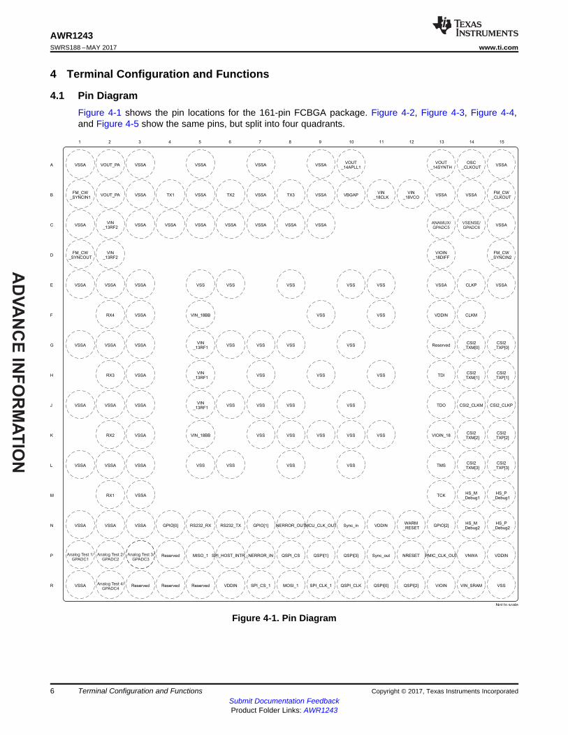
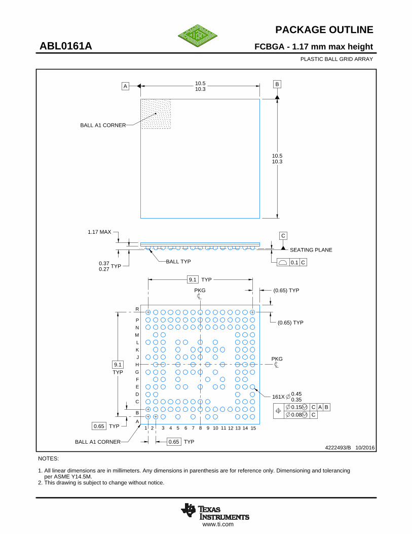
4.1 Pin DiagramFigure 4-1 shows the pin locations for the 161-pin FCBGA package. Figure 4-2, Figure 4-3, Figure 4-4,and Figure 4-5 show the same pins, but split into four quadrants.

Figure 4-1. Pin Diagram

AD

VA

NC

E I

NF

OR

MA

TIO

N

9 10 11 12 13 14 15

A

B

C

D

E

F

G

Not to scale

VSSAVOUT

_14APLL1

VOUT

_14SYNTH

OSC

_CLKOUTVSSA

VSSA VBGAPVIN

_18CLK

VIN

_18VCOVSSA VSSA

FM_CW

_CLKOUT

VSSA VSSA

VIOIN

_18DIFF

FM_CW

_SYNCIN2

VSS VSS VSSA CLKP VSSA

VSS VSS VDDIN CLKM

VSS ReservedCSI2

_TXM[0]

CSI2

_TXP[0]

1

3

2

4

ANAMUX/

GPADC5

VSENSE/

GPADC6

1 2 3 4 5 6 7 8

A

B

C

D

E

F

G

Not to scale

VSSA VOUT_PA VSSA VSSA VSSA

FM_CW_SYNCIN1 VOUT_PA VSSA TX1 VSSA TX2 VSSA TX3

VSSA VIN_13RF2 VSSA VSSA VSSA VSSA VSSA VSSA

FM_CW_SYNCOUT

VIN_13RF2

VSSA VSSA VSSA VSS VSS VSS

RX4 VSSA VIN_18BB

VSSA VSSA VSSA VIN_13RF1 VSS VSS VSS

1

3

2

4

7

AWR1243www.ti.com SWRS188 –MAY 2017

Submit Documentation FeedbackProduct Folder Links: AWR1243

Terminal Configuration and FunctionsCopyright © 2017, Texas Instruments Incorporated

Figure 4-2. Top Left Quadrant

Figure 4-3. Top Right Quadrant

AD

VA

NC

E IN

FO

RM

AT

ION

1 2 3 4 5 6 7 8

H

J

K

L

M

N

P

R

Not to scale

RX3 VSSAVIN

_13RF1VSS

VSSA VSSA VSSAVIN

_13RF1VSS VSS VSS

RX2 VSSA VIN_18BB VSS VSS

VSSA VSSA VSSA VSS VSS VSS

RX1

VSSA VSSA VSSA GPIO[0] RS232_RX RS232_TX GPIO[1] NERROR_OUT

Reserved MISO_1 SPI_HOST_INTR_1NERROR_IN QSPI_CS

VSSA Reserved Reserved Reserved VDDIN SPI_CS_1 MOSI_1

1

3

2

4

VSSA

Analog Test 1/GPADC1

Analog Test 2/GPADC2

Analog Test 3/GPADC3

Analog Test 4/GPADC4

8

AWR1243SWRS188 –MAY 2017 www.ti.com

Submit Documentation FeedbackProduct Folder Links: AWR1243

Terminal Configuration and Functions Copyright © 2017, Texas Instruments Incorporated

Figure 4-4. Bottom Left Quadrant

AD

VA

NC

E I

NF

OR

MA

TIO

N

9 10 11 12 13 14 15

H

J

K

L

M

N

P

R

Not to scale

VSS VSS TDI CSI2_TXM[1]

CSI2_TXP[1]

VSS TDO CSI2_CLKM CSI2_CLKP

VSS VSS VSS VIOIN_18 CSI2_TXM[2]

CSI2_TXP[2]

VSS TMS CSI2_TXM[3]

CSI2_TXP[3]

TCK HS_M_Debug1

HS_P_Debug1

MCU_CLK_OUT Sync_in VDDIN WARM_RESET GPIO[2] HS_M

_Debug2HS_P

_Debug2

QSPI[1] QSPI[3] Sync_out NRESET PMIC_CLK_OUT VNWA VDDIN

SPI_CLK_1 QSPI_CLK QSPI[0] QSPI[2] VIOIN VIN_SRAM VSS

1

3

2

4

9

AWR1243www.ti.com SWRS188 –MAY 2017

Submit Documentation FeedbackProduct Folder Links: AWR1243

Terminal Configuration and FunctionsCopyright © 2017, Texas Instruments Incorporated

Figure 4-5. Bottom Right Quadrant

AD

VA

NC

E IN

FO

RM

AT

ION

10

AWR1243SWRS188 –MAY 2017 www.ti.com

Submit Documentation FeedbackProduct Folder Links: AWR1243

Terminal Configuration and Functions Copyright © 2017, Texas Instruments Incorporated

4.2 Signal DescriptionsTable 4-1 lists the pins by function and describes that function.

Table 4-1. Signal Descriptions

FUNCTION SIGNAL NAME PIN NUMBER PINTYPE DESCRIPTION

TransmittersTX1 B4 O Single-ended transmitter1 o/pTX2 B6 O Single-ended transmitter2 o/pTX3 B8 O Single-ended transmitter3 o/p

Receivers

RX1 M2 I Single-ended receiver1 i/pRX2 K2 I Single-ended receiver2 i/pRX3 H2 I Single-ended receiver3 i/pRX4 F2 I Single-ended receiver4 i/p

CSI2 TX

CSI2_TXP[0] G15 ODifferential data Out – Lane 0

CSI2_TXM[0] G14 OCSI2_CLKP J15 O

Differential clock OutCSI2_CLKM J14 OCSI2_TXP[1] H15 O

Differential data Out – Lane 1CSI2_TXM[1] H14 OCSI2_TXP[2] K15 O

Differential data Out – Lane 2CSI2_TXM[2] K14 OCSI2_TXP[3] L15 O

Differential data Out – Lane 3CSI2_TXM[3] L14 OHS_DEBUG1_P M15 O

Differential debug port 1HS_DEBUG1_M M14 OHS_DEBUG2_P N15 O

Differential debug port 2HS_DEBUG2_M N14 O

Chip-to-chipcascadingsynchronizationsignals

FM_CW_CLKOUT B15 O 20-GHz single-ended output. Modulated waveformFM_CW_SYNCIN1 B1 I 20-GHz single-ended input. Only one of these pins should be

used. Multiple instances for layout flexibility.FM_CW_SYNCIN2 D15 IFM_CW_SYNCOUT D1 O 20-GHz single-ended output for onboard loopback if desired

Systemsynchronization

SYNC_OUT P11 O Low-frequency synchronization signal outputSYNC_IN N10 I Low-frequency synchronization signal input

SPI controlinterface fromexternal MCU(default slavemode)

SPI_CS_1 R7 I SPI chip selectSPI_CLK_1 R9 I SPI clockMOSI_1 R8 I SPI data inputMISO_1 P5 O SPI data outputSPI_HOST_INTR_1 P6 O SPI interrupt to hostRESERVED R3, R4, R5, P4

Reset

NRESET P12 I Power on reset for chip. Active low

WARM_RESET N12 IOOpen-drain fail-safe warm reset signal. Can be driven fromPMIC for diagnostic or can be used as status signal that thedevice is going through reset.

Safety

NERROR_OUT N8 OOpen-drain fail-safe output signal. Connected toPMIC/Processor/MCU to indicate that some severe criticalityfault has happened. Recovery would be through reset.

NERROR_IN P7 I

Fail-safe input to the device. Error output from any other devicecan be concentrated in the error signaling monitor moduleinside the device and appropriate action can be taken byfirmware

AD

VA

NC

E I

NF

OR

MA

TIO

N

11

AWR1243www.ti.com SWRS188 –MAY 2017

Submit Documentation FeedbackProduct Folder Links: AWR1243

Terminal Configuration and FunctionsCopyright © 2017, Texas Instruments Incorporated

Table 4-1. Signal Descriptions (continued)

FUNCTION SIGNAL NAME PIN NUMBER PINTYPE DESCRIPTION

JTAG

TMS L13 I

JTAG port for standard boundary scanTCK M13 ITDI H13 ITDO J13 O

Referenceoscillator

CLKP E14 ICLKP is the Input and CLKM is the Output to drive crystal

CLKM F14 O

Reference clock OSC_CLKOUT A14 O Reference clock output from clocking subsystem after cleanupPLL. Can be used by slave chip in multichip cascading

Band-gap voltage VBGAP B10 O

Power supply

VDDIN F13,N11,P15,R6 POW 1.2-V digital power supply

VIN_SRAM R14 POW 1.2-V power rail for internal SRAMVNWA P14 POW 1.2-V power rail for SRAM array back bias

VIOIN R13 POW I/O supply (3.3-V or 1.8-V): All CMOS I/Os would operate onthis supply.

VIOIN_18 K13 POW 1.8-V supply for CMOS IOVIN_18CLK B11 POW 1.8-V supply for clock moduleVIOIN_18DIFF D13 POW 1.8-V supply for CSI2 portReserved G13 POW No connectVIN_13RF1 G5,J5,H5 POW 1.3-V Analog and RF supply,VIN_13RF1 and VIN_13RF2

could be shorted on the boardVIN_13RF2 C2,D2 POWVIN_18BB K5,F5 POW 1.8-V Analog baseband power supplyVIN_18VCO B12 POW 1.8-V RF VCO supply

VSS

E5,E6,E8,E10,E11,F9,F11,G6,G7,G8,G10,H7,H9,H11,J6,J7,J8,J10,K7,K8,K9,K10,K11,L5,L6,L8,L10,

R15

GND Digital ground

VSSA

A1,A3,A5,A7,A9,A15,B3,B5,B7,B9,B13,B14,C1,C3,C4,C5,C6,C7,C8,C9,C15,E1,E2,E3,E13,E15,F3,G1,G2,G3,H3,J1,J2,J3,K3,L1,L

2,L3,M3,N1,N2,N3,

R1

GND Analog ground

Internal LDOoutput/inputs

VOUT_14APLL1 A10 OVOUT_14SYNTH A13 OVOUT_PA A2,B2 O

External clock outPMIC_CLK_OUT P13 O Dithered clock input to PMIC

MCU_CLK_OUT N9 O Programmable clock given out to external MCU or theprocessor

General-purposeI/Os

GPIO[0] N4 IO General-purpose IOGPIO[1] N7 IO General-purpose IOGPIO[2] N13 IO General-purpose IO

AD

VA

NC

E IN

FO

RM

AT

ION

12

AWR1243SWRS188 –MAY 2017 www.ti.com

Submit Documentation FeedbackProduct Folder Links: AWR1243

Terminal Configuration and Functions Copyright © 2017, Texas Instruments Incorporated

Table 4-1. Signal Descriptions (continued)

FUNCTION SIGNAL NAME PIN NUMBER PINTYPE DESCRIPTION

(1) This option is for development/debug in preproduction phase. Can be disabled by firmware pin mux setting.

QSPI for SerialFlash (1)

QSPI_CS P8 O Chip-select output from the device. Device is a masterconnected to serial flash slave.

QSPI_CLK R10 O Clock output from the device. Device is a master connected toserial flash slave.

QSPI[0] R11 IO Data IN/OUTQSPI[1] P9 IO Data IN/OUTQSPI[2] R12 IO Data IN/OUTQSPI[3] P10 IO Data IN/OUT

Flash programmingand RS232UART (1)

RS232_TX N6 O UART pins for programming external flash inpreproduction/debug hardware.RS232_RX N5 I

Test and Debugoutput forpreproductionphase. Can bepinned out onproductionhardware for fielddebug

Analog Test1 / GPADC1 P1 IO GP ADC channel 1Analog Test2 / GPADC2 P2 IO GP ADC channel 2Analog Test3 / GPADC3 P3 IO GP ADC channel 3Analog Test4 / GPADC4 R2 IO GP ADC channel 4ANAMUX / GPADC5 C13 IO GP ADC channel 5VSENSE / GPADC6 C14 IO GP ADC channel 6

AD

VA

NC

E I

NF

OR

MA

TIO

N

13

AWR1243www.ti.com SWRS188 –MAY 2017

Submit Documentation FeedbackProduct Folder Links: AWR1243

SpecificationsCopyright © 2017, Texas Instruments Incorporated

(1) Stresses beyond those listed under Absolute Maximum Ratings may cause permanent damage to the device. These are stress ratingsonly, and functional operation of the device at these or any other conditions beyond those indicated under Recommended OperatingConditions is not implied. Exposure to absolute-maximum-rated conditions for extended periods may affect device reliability.

(2) All voltage values are with respect to VSS, unless otherwise noted.

5 Specifications

5.1 Absolute Maximum Ratings (1) (2)

over operating free-air temperature range (unless otherwise noted)MIN MAX UNIT

VDDIN 1.2 V digital power supply –0.5 1.4 VVIN_SRAM 1.2 V power rail for internal SRAM –0.5 1.4 VVNWA 1.2 V power rail for SRAM array back bias –0.5 1.4 V

VIOIN I/O supply (3.3 V or 1.8 V): All CMOS I/Os would operate on thissupply. –0.5 3.8 V

VIOIN_18 1.8 V supply for CMOS IO –0.5 2 VVIN_18CLK 1.8 V supply for clock module –0.5 2 VVIOIN_18DIFF 1.8 V supply for CSI2 port –0.5 2 V

VIN_13RF1 1.3 V Analog and RF supply,VIN_13RF1 and VIN_13RF2 couldbe shorted on the board. –0.5 1.45 V

VIN_13RF2 –0.5 1.45 V

VIN_13RF1(1-V LDO bypassmode)

Device supports mode where external Power Management blockcan supply 1 V on VIN_13RF1 and VIN_13RF2 rails. In thisconfiguration, the internal LDO of the device would be keptbypassed.

–0.5 1.4 V

VIN_13RF2(1-V Internal LDObypass mode)

–0.5 1.4 V

VIN_18BB 1.8-V Analog baseband power supply –0.5 2 VVIN_18VCO supply 1.8-V RF VCO supply –0.5 2 V

Input and outputvoltage range

Dual-voltage LVCMOS inputs, 3.3 V or 1.8 V (Steady State) –0.3V VIOIN + 0.3VDual-voltage LVCMOS inputs, operated at 3.3 V/1.8 V

(Transient Overshoot/Undershoot)VIOIN + 20% up to

20% of signal periodCLKP, CLKM Input ports for reference crystal –0.5 2 V

Clamp currentInput or Output Voltages 0.3 V above or below their respectivepower rails. Limit clamp current that flows through the internaldiode protection cells of the I/O.

–20 20 mA

TJ Operating junction temperature range –40 125 ºCTSTG Storage temperature range after soldered onto PC board –55 150 ºC

(1) AEC Q100-002 indicates that HBM stressing shall be in accordance with the ANSI/ESDA/JEDEC JS-001 specification.

5.2 ESD RatingsVALUE UNIT

V(ESD) Electrostatic dischargeHuman-body model (HBM), per AEC Q100-002 (1) ±1000

VCharged-device model (CDM), per AEC Q100-011 ±250

(1) This information is provided solely for your convenience and does not extend or modify the warranty provided under TI's standard termsand conditions for TI semiconductor products.

5.3 Power-On Hours (POH) (1)

OPERATINGCONDITION NOMINAL CVDD VOLTAGE (V) JUNCTION

TEMPERATURE (Tj)POWER-ON HOURS [POH] (HOURS)

100% duty cycle 1.2

–40°C 600 (6%)75°C 2000 (20%)95°C 6500 (65%)

105°C 900 (9%)

AD

VA

NC

E IN

FO

RM

AT

ION

14

AWR1243SWRS188 –MAY 2017 www.ti.com

Submit Documentation FeedbackProduct Folder Links: AWR1243

Specifications Copyright © 2017, Texas Instruments Incorporated

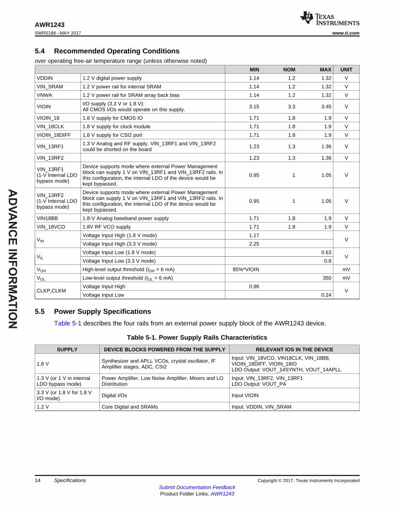
5.4 Recommended Operating Conditionsover operating free-air temperature range (unless otherwise noted)

MIN NOM MAX UNITVDDIN 1.2 V digital power supply 1.14 1.2 1.32 VVIN_SRAM 1.2 V power rail for internal SRAM 1.14 1.2 1.32 VVNWA 1.2 V power rail for SRAM array back bias 1.14 1.2 1.32 V

VIOIN I/O supply (3.3 V or 1.8 V):All CMOS I/Os would operate on this supply. 3.15 3.3 3.45 V

VIOIN_18 1.8 V supply for CMOS IO 1.71 1.8 1.9 VVIN_18CLK 1.8 V supply for clock module 1.71 1.8 1.9 VVIOIN_18DIFF 1.8 V supply for CSI2 port 1.71 1.8 1.9 V

VIN_13RF1 1.3 V Analog and RF supply. VIN_13RF1 and VIN_13RF2could be shorted on the board 1.23 1.3 1.36 V

VIN_13RF2 1.23 1.3 1.36 V

VIN_13RF1(1-V Internal LDObypass mode)

Device supports mode where external Power Managementblock can supply 1 V on VIN_13RF1 and VIN_13RF2 rails. Inthis configuration, the internal LDO of the device would bekept bypassed.

0.95 1 1.05 V

VIN_13RF2(1-V Internal LDObypass mode)

Device supports mode where external Power Managementblock can supply 1 V on VIN_13RF1 and VIN_13RF2 rails. Inthis configuration, the internal LDO of the device would bekept bypassed.

0.95 1 1.05 V

VIN18BB 1.8-V Analog baseband power supply 1.71 1.8 1.9 VVIN_18VCO 1.8V RF VCO supply 1.71 1.8 1.9 V

VIHVoltage Input High (1.8 V mode) 1.17

VVoltage Input High (3.3 V mode) 2.25

VILVoltage Input Low (1.8 V mode) 0.63

VVoltage Input Low (3.3 V mode) 0.8

VOH High-level output threshold (IOH = 6 mA) 85%*VIOIN mVVOL Low-level output threshold (IOL = 6 mA) 350 mV

CLKP,CLKMVoltage Input High 0.96

VVoltage Input Low 0.24

5.5 Power Supply SpecificationsTable 5-1 describes the four rails from an external power supply block of the AWR1243 device.

Table 5-1. Power Supply Rails Characteristics

SUPPLY DEVICE BLOCKS POWERED FROM THE SUPPLY RELEVANT IOS IN THE DEVICE

1.8 V Synthesizer and APLL VCOs, crystal oscillator, IFAmplifier stages, ADC, CSI2

Input: VIN_18VCO, VIN18CLK, VIN_18BB,VIOIN_18DIFF, VIOIN_18IOLDO Output: VOUT_14SYNTH, VOUT_14APLL

1.3 V (or 1 V in internalLDO bypass mode)

Power Amplifier, Low Noise Amplifier, Mixers and LODistribution

Input: VIN_13RF2, VIN_13RF1LDO Output: VOUT_PA

3.3 V (or 1.8 V for 1.8 VI/O mode) Digital I/Os Input VIOIN

1.2 V Core Digital and SRAMs Input: VDDIN, VIN_SRAM

AD

VA

NC

E I

NF

OR

MA

TIO

N

15

AWR1243www.ti.com SWRS188 –MAY 2017

Submit Documentation FeedbackProduct Folder Links: AWR1243

SpecificationsCopyright © 2017, Texas Instruments Incorporated

Table 5-2 lists tolerable ripple specifications for 1.3-V (1.0-V) and 1.8-V supply rails.

Table 5-2. Ripple Specifications

FREQUENCY (kHz)RF RAIL VCO/IF RAIL

1.0 V (INTERNAL LDO BYPASS)(µVRMS) 1.3 V (µVRMS) 1.8 V (µVRMS)

137.5 7.76 648.73 83.41275 5.83 76.48 21.27550 3.44 22.74 11.43

1100 2.53 4.05 6.732200 11.29 82.44 13.394200 13.65 93.35 19.706600 22.91 117.78 29.63

5.6 Power Consumption SummaryTable 5-3 and Table 5-4 summarize the power consumption at the power terminals.

Table 5-3. Maximum Current Ratings at Power Terminals

PARAMETER SUPPLY NAME DESCRIPTION MIN TYP MAX UNIT

Current consumption

VDDIN, VIN_SRAM, VNWATotal current drawn byall nodes driven by1.2V rail

500

mA

VIN_13RF1, VIN_13RF2Total current drawn byall nodes driven by1.3V rail

2000

VIOIN_18, VIN_18CLK,VIOIN_18DIFF, VIN_18BB,VIN_18VCO

Total current drawn byall nodes driven by1.8V rail

850

VIOINTotal current drawn byall nodes driven by3.3V rail

50

Table 5-4. Average Power Consumption at Power Terminals

PARAMETER CONDITION DESCRIPTION MIN TYP MAX UNIT

Average powerconsumption

1.0-V internalLDO bypassmode

1TX, 4RXSampling: 16.66 MSps complexTransceiver, 40-ms frame time, 512chirps, 512 samples/chirp, 8.5-μsinterchirp time (50% duty cycle)Data Port: MIPI-CSI-2

1.73

W2TX, 4RX 1.88

1.3-V internalLDO enabledmode

1TX, 4RX 1.92

2TX, 4RX 2.1

AD

VA

NC

E IN

FO

RM

AT

ION

RX Gain (dB)

NF

(dB

)

IB P

1dB

(dB

m)

24 26 28 30 32 34 36 38 40 42 44 46 4813.5 -48

13.8 -44

14.1 -40

14.4 -36

14.7 -32

15 -28

15.3 -24

15.6 -20NF (db)IB P1db (dBm)

16

AWR1243SWRS188 –MAY 2017 www.ti.com

Submit Documentation FeedbackProduct Folder Links: AWR1243

Specifications Copyright © 2017, Texas Instruments Incorporated

(1) The analog IF stages include high-pass filtering, with two independently configurable first-order high-pass corner frequencies. The set ofavailable HPF corners is summarized as follows:

Available HPF Corner Frequencies (kHz)HPF1 HPF2175, 235, 350, 700 350, 700, 1400, 2800

The filtering performed by the baseband chain is targeted to provide:• Less than ±0.5 dB pass-band ripple/droop, and• Better than 60 dB anti-aliasing attenuation for any frequency that can alias back into the pass-band.

5.7 RF Specificationover recommended operating conditions (unless otherwise noted)

PARAMETER MIN TYP MAX UNIT

Receiver

Noise figure76 to 77 GHz 15

dB77 to 81 GHz 16

1-dB compression point –5 dBmMaximum gain step 48 dBGain range 24 dBGain step size 2 dBIQ gain mismatch 1 dBIQ phase mismatch 2 degreeIF bandwidth (1) 15 MHzA2D sampling rate (real) 37.5 MspsA2D sampling rate (complex) 18.75 MspsA2D resolution 12 Bits

TransmitterOutput power 12 dBmAmplitude noise –145 dBc/Hz

Clocksubsystem

Frequency range 76 81 GHzRamp rate 100 MHz/µs

Phase noise at 1-MHz offset76 to 77 GHz –94

dBc/Hz77 to 81 GHz –91

Figure 5-1 shows variations of noise figure and in-band P1dB parameters with respect to receiver gainprogrammed.

Figure 5-1. Noise Figure, In-band P1dB vs Receiver Gain

Table 5-5 describes the CSI-2 DPHY electrical specifications.

AD

VA

NC

E I

NF

OR

MA

TIO

N

17

AWR1243www.ti.com SWRS188 –MAY 2017

Submit Documentation FeedbackProduct Folder Links: AWR1243

SpecificationsCopyright © 2017, Texas Instruments Incorporated

(1) Value when driving into differential load impedance anywhere in the range from 80 to 125 Ω.

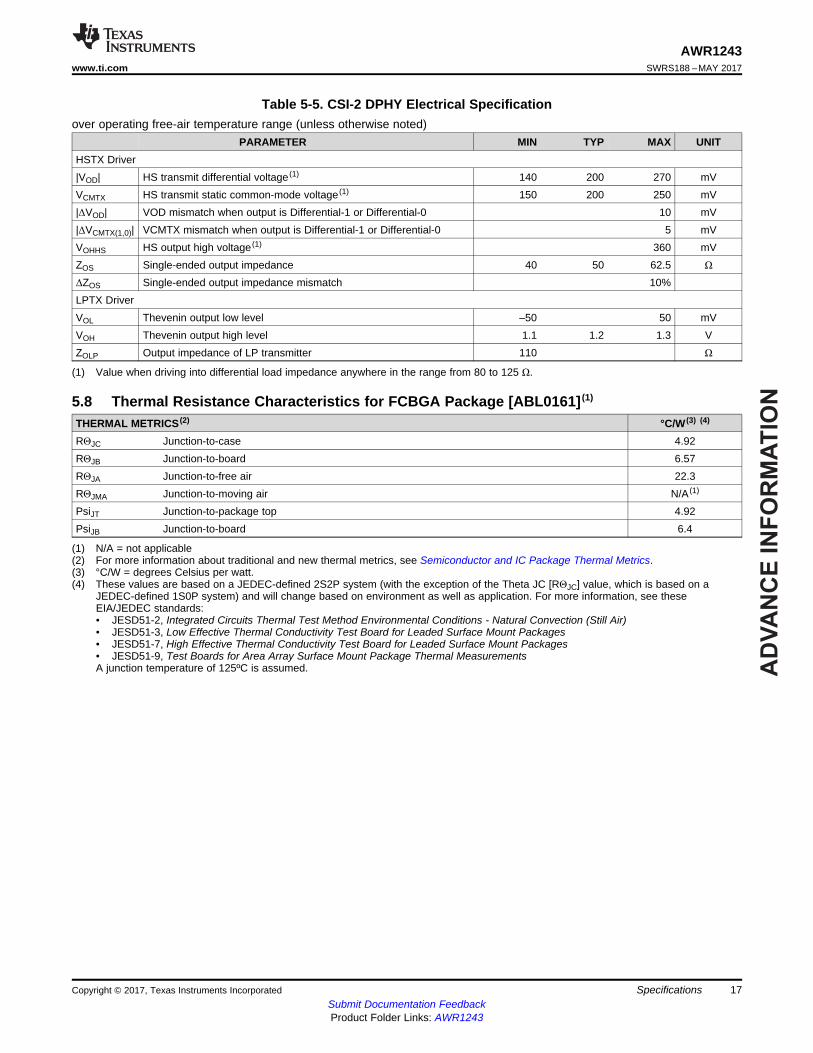
Table 5-5. CSI-2 DPHY Electrical Specificationover operating free-air temperature range (unless otherwise noted)

PARAMETER MIN TYP MAX UNITHSTX Driver|VOD| HS transmit differential voltage (1) 140 200 270 mVVCMTX HS transmit static common-mode voltage (1) 150 200 250 mV|ΔVOD| VOD mismatch when output is Differential-1 or Differential-0 10 mV|ΔVCMTX(1,0)| VCMTX mismatch when output is Differential-1 or Differential-0 5 mVVOHHS HS output high voltage (1) 360 mVZOS Single-ended output impedance 40 50 62.5 Ω

ΔZOS Single-ended output impedance mismatch 10%LPTX DriverVOL Thevenin output low level –50 50 mVVOH Thevenin output high level 1.1 1.2 1.3 VZOLP Output impedance of LP transmitter 110 Ω

(1) N/A = not applicable(2) For more information about traditional and new thermal metrics, see Semiconductor and IC Package Thermal Metrics.(3) °C/W = degrees Celsius per watt.(4) These values are based on a JEDEC-defined 2S2P system (with the exception of the Theta JC [RΘJC] value, which is based on a

JEDEC-defined 1S0P system) and will change based on environment as well as application. For more information, see theseEIA/JEDEC standards:• JESD51-2, Integrated Circuits Thermal Test Method Environmental Conditions - Natural Convection (Still Air)• JESD51-3, Low Effective Thermal Conductivity Test Board for Leaded Surface Mount Packages• JESD51-7, High Effective Thermal Conductivity Test Board for Leaded Surface Mount Packages• JESD51-9, Test Boards for Area Array Surface Mount Package Thermal MeasurementsA junction temperature of 125ºC is assumed.

5.8 Thermal Resistance Characteristics for FCBGA Package [ABL0161] (1)

THERMAL METRICS (2) °C/W (3) (4)

RΘJC Junction-to-case 4.92RΘJB Junction-to-board 6.57RΘJA Junction-to-free air 22.3RΘJMA Junction-to-moving air N/A (1)

PsiJT Junction-to-package top 4.92PsiJB Junction-to-board 6.4

AD

VA

NC

E IN

FO

RM

AT

ION

Reference Clock Stabilization time

~5mS

FUSE_SHIFT_EN

PORZ_1P8V Controls HHV of IO

PORZ_TOP/ GEN_TOP

EFC_READY

XTAL_DET_STAT

XTAL_EN/ SLICER_EN

SLICER_REF_CLK(CLKP+CLKM thru’ SLICER)

LIMP_MODE_STATUS

CPU CLK is REF CLK if STATUS is 1ELSE INT_RCOSC_CLK if STATUS is 0

Reset Control to Top Digital and Analog

Wake Up Done

Reset Control to Digital Processor and Analog/RF

Internal Signals

Mentioned for reference only

*Names are representative

CPU_CLK

~400 cycles

PORZ_CPU/PORZ_DIG/

GEN_ANA

1 IF REF CLK is NOT PRESENT

XTAL STATUS 1 if XTAL FOUND/ ‘0’ if EXTERNAL CLK is FORCED

~5mS

(VDDIN)

(VIN_*)

(VIOIN_18DIFF)

(VIOIN)

(NRESET)

PMIC_OUT,SYNC_OUT, TDO

001 (Functional) CAN BE CHANGED.

Includes ramping of all other supplies VIN_18BB, VIN_18CLK, VIN_13RF*,VIOIN_18DIFF

MCU_CLK_OUT

Includes ramping of VIOIN_18

External Signals

3mS

(1)

18

AWR1243SWRS188 –MAY 2017 www.ti.com

Submit Documentation FeedbackProduct Folder Links: AWR1243

Specifications Copyright © 2017, Texas Instruments Incorporated

5.9 Timing and Switching Characteristics

5.9.1 Power Supply Sequencing and Reset TimingThe AWR1243 device expects all external voltage rails to be stable before reset is deasserted. Figure 5-2describes the device wake-up sequence.

(1) MCU_CLK_OUT in autonomous mode, where AWR1243 application is booted from the serial flash, MCU_CLK_OUT is not enabledby default by the device bootloader.

Figure 5-2. Device Wake-up Sequence

AD

VA

NC

E I

NF

OR

MA

TIO

N

f2

L f1 P

f1 f2

CC C C

C C= ´ +

+

40 / 50 MHz

XTALP

XTALM

Cf1

Cf2

Cp

19

AWR1243www.ti.com SWRS188 –MAY 2017

Submit Documentation FeedbackProduct Folder Links: AWR1243

SpecificationsCopyright © 2017, Texas Instruments Incorporated

(1) The crystal manufacturer's specification must satisfy this requirement.(2) Includes initial tolerance of the crystal, drift over temperature, aging and frequency pulling due to incorrect load capacitance.

5.9.2 Input Clocks and Oscillators

5.9.2.1 Clock Specifications

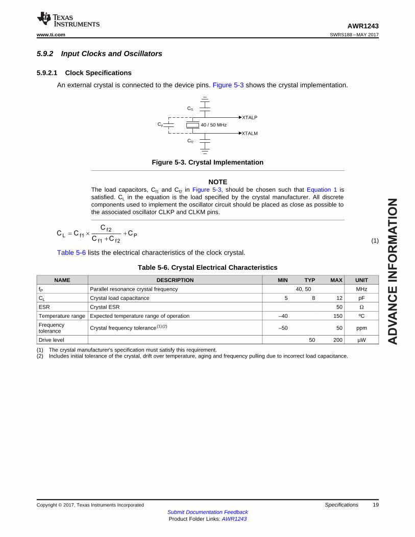
An external crystal is connected to the device pins. Figure 5-3 shows the crystal implementation.

Figure 5-3. Crystal Implementation

NOTEThe load capacitors, Cf1 and Cf2 in Figure 5-3, should be chosen such that Equation 1 issatisfied. CL in the equation is the load specified by the crystal manufacturer. All discretecomponents used to implement the oscillator circuit should be placed as close as possible tothe associated oscillator CLKP and CLKM pins.

(1)

Table 5-6 lists the electrical characteristics of the clock crystal.

Table 5-6. Crystal Electrical Characteristics

NAME DESCRIPTION MIN TYP MAX UNITfP Parallel resonance crystal frequency 40, 50 MHzCL Crystal load capacitance 5 8 12 pFESR Crystal ESR 50 Ω

Temperature range Expected temperature range of operation –40 150 ºCFrequencytolerance Crystal frequency tolerance (1) (2) –50 50 ppm

Drive level 50 200 µW

AD

VA

NC

E IN

FO

RM

AT

ION

20

AWR1243SWRS188 –MAY 2017 www.ti.com

Submit Documentation FeedbackProduct Folder Links: AWR1243

Specifications Copyright © 2017, Texas Instruments Incorporated

5.9.3 Multibuffered / Standard Serial Peripheral Interface (MibSPI)

5.9.3.1 Peripheral Description

The MibSPI/SPI is a high-speed synchronous serial input/output port that allows a serial bit stream to beshifted into and out of the device at a programmed bit-transfer rate. The MibSPI/SPI is normally used forcommunication between the microcontroller and external peripherals or another microcontroller.

Table 5-8 and Table 5-9 assume the operating conditions stated in Table 5-7. Table 5-8, Table 5-9, andFigure 5-4 describe the timing and switching characteristics of the MibSPI transmit and receive RAMorganization.

Table 5-7. SPI Timing ConditionsMIN TYP MAX UNIT

Input ConditionstR Input rise time 1 3 nstF Input fall time 1 3 nsOutput ConditionsCLOAD Output load capacitance 2 15 pF

(1) The mode of operation is mode 0 (clock polarity = 0 ; clock phase = 0).

Table 5-8. SPI Slave Mode Switching Parameters (SPICLK = input, SPISIMO = input,and SPISOMI = output) (1)

NO. PARAMETER MIN TYP MAX UNIT1 tc(SPC)S Cycle time, SPICLK 25 ns2 tw(SPCH)S Pulse duration, SPICLK high (clock polarity = 0) 10 ns3 tw(SPCL)S Pulse duration, SPICLK low (clock polarity = 0) 10 ns

4 td(SPCH-SOMI)SDelay time, SPISOMI valid after SPICLK high(clock polarity = 0) 10 ns

5 th(SPCH-SOMI)SHold time, SPISOMI data valid after SPICLK high(clock polarity = 0) 2 ns

Table 5-9. SPI Slave Mode Timing Requirements (SPICLK = input, SPISIMO = input,and SPISOMI = output)

NO. MIN TYP MAX UNIT1 tsu(SIMO-SPCL)S Setup time, SPISIMO before SPICLK low (clock polarity = 0) 3 ns2 th(SPCL-SIMO)S Hold time, SPISIMO data valid after SPICLK low (clock polarity = 0) 0 ns

AD

VA

NC

E I

NF

OR

MA

TIO

N

SPISIMO DataMust Be Valid

SPISOMI Data Is Valid

6

7

2

1

3

SPICLK(clock polarity = 0)

SPICLK(clock polarity = 1)

SPISOMI

SPISIMO

5 4

21

AWR1243www.ti.com SWRS188 –MAY 2017

Submit Documentation FeedbackProduct Folder Links: AWR1243

SpecificationsCopyright © 2017, Texas Instruments Incorporated

Figure 5-4. SPI Slave Mode External Timing

AD

VA

NC

E IN

FO

RM

AT

ION

CS

CLK

MOSI

MISO

IRQ

0x56780x1234 0x4321 CRC

0xDCBA 0xABCD CRC

0x8765

16 bytes

2 SPI clocks

22

AWR1243SWRS188 –MAY 2017 www.ti.com

Submit Documentation FeedbackProduct Folder Links: AWR1243

Specifications Copyright © 2017, Texas Instruments Incorporated

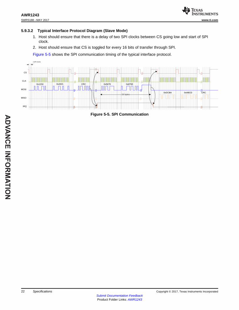
5.9.3.2 Typical Interface Protocol Diagram (Slave Mode)1. Host should ensure that there is a delay of two SPI clocks between CS going low and start of SPI

clock.2. Host should ensure that CS is toggled for every 16 bits of transfer through SPI.

Figure 5-5 shows the SPI communication timing of the typical interface protocol.

Figure 5-5. SPI Communication

AD

VA

NC

E I

NF

OR

MA

TIO

N

23

AWR1243www.ti.com SWRS188 –MAY 2017

Submit Documentation FeedbackProduct Folder Links: AWR1243

SpecificationsCopyright © 2017, Texas Instruments Incorporated

(1) Slew control, which is configured by PADxx_CFG_REG, changes behavior of the output driver (faster or slower output slew rate).(2) The rise/fall time is measured as the time taken by the signal to transition from 10% and 90% of VIOIN voltage.

5.9.4 General-Purpose Input/OutputTable 5-10 lists the switching characteristics of output timing relative to load capacitance.

Table 5-10. Switching Characteristics for Output Timing versus Load Capacitance (CL) (1) (2)

PARAMETER TEST CONDITIONS VIOIN = 1.8V VIOIN = 3.3V UNIT

tr Max rise time

Slew control = 0

CL = 20 pF 2.878 3.013nsCL = 50 pF 6.446 6.947

CL = 75 pF 9.43 10.249

tf Max fall timeCL = 20 pF 2.827 2.883

nsCL = 50 pF 6.442 6.687CL = 75 pF 9.439 9.873

tr Max rise time

Slew control = 1

CL = 20 pF 3.307 3.389nsCL = 50 pF 6.77 7.277

CL = 75 pF 9.695 10.57

tf Max fall timeCL = 20 pF 3.128 3.128

nsCL = 50 pF 6.656 6.656CL = 75 pF 9.605 9.605

AD

VA

NC

E IN

FO

RM

AT

ION

24

AWR1243SWRS188 –MAY 2017 www.ti.com

Submit Documentation FeedbackProduct Folder Links: AWR1243

Specifications Copyright © 2017, Texas Instruments Incorporated

(1) With an additional load capacitance CCM of 0 to 60 pF on the termination center tap at RX side of the lane(2) While driving CLOAD. Load capacitance includes 50 pF of transmission line capacitance, and 10 pF each for TX and RX.(3) When the output voltage is from 15% to 85% of the fully settled LP signal levels(4) Measured as average across any 50 mV segment of the output signal transition

5.9.5 Camera Serial Interface (CSI)The CSI is a MIPI D-PHY compliant interface for connecting this device to a camera receiver module. Thisinterface is made of four differential lanes; each lane is configurable for carrying data or clock. The polarityof each wire of a lane is also configurable. Table 5-11, Figure 5-6, Figure 5-7, and Figure 5-8 describe theclock and data timing of the CSI.

Table 5-11. CSI Switching Characteristicsover operating free-air temperature range (unless otherwise noted)

PARAMETER MIN TYP MAX UNITHPTX

HSTXDBR Data bit rate(1 or 2 data lane PHY) 150 900

Mbps(4 data lane PHY) 150 600

fCLK DDR clock frequency(1 or 2 data lane PHY) 75 450

MHz(4 data lane PHY) 75 300

ΔVCMTX(LF)Common-level variation from 75 to 450 MHz of CSI2 clockfrequency –50 50 mVpeak

tR and tF 20% to 80% rise time and fall time150 ns

0.3 UILPTX DRIVERtRLP and tFLP 15% to 85% rise time and fall time 25 ns

tEOT(1) Time from start of THS-TRAIL period to start of LP-11 state 105 +

12*UI ns

δV/δtSR(2) (3) (4)

Slew rate. CLOAD = 0 to 5 pF 500mV/nsSlew rate. CLOAD = 5 to 20 pF 200

Slew rate. CLOAD = 20 to 70 pF 100CLOAD

(2) Load capacitance 0 70 pFDATA-CLOCK Timing Specification

UINOMNominal unit interval (1, 2, or 3 data lane PHY) 1.11 13.33

nsNominal unit interval (4 data lane PHY) 1.67 13.33

UIINST,MINMinimum instantaneous Unit Interval (1, 2, or 3 data lane PHY) 1.033

0.975*UINOM –

0.05 ns

Minimum instantaneous Unit Interval (4 data lane PHY) 1.131

TSKEW[TX] Data to clock skew measured at transmitter –0.15 0.15 UIINST,MIN

CSI2 TIMING SPECIFICATION

TCLK-MISSTime-out for receiver to detect absence of clock transitions anddisable the clock lane HS-RX. 60 ns

TCLK-POST

Time that the transmitter continues to send HS clock after thelast associated data lane has transitioned to lp mode. Interval isdefined as the period from the end of THS-TRAIL to the beginningof TCLK-TRAIL.

60 ns +52*UI ns

TCLK-PRE

Time that the HS clock shall be driven by the transmitter beforeany associated data lane beginning the transition from LP to HSmode.

8 ns

TCLK-PREPARE

Time that the transmitter drives the clock lane LP-00 line stateimmediately before the HS-0 line state starting the HStransmission.

38 95 ns

TCLK-SETTLE

Time interval during which the HS receiver should ignore anyclock lane HS transitions, starting from the beginning of TCLK-PREPARE.

95 300 ns

AD

VA

NC

E I

NF

OR

MA

TIO

N

CSI2_CLK(P/M)

CSI2_TX(P/M)

1 UI

0.5UI + Tskew

25

AWR1243www.ti.com SWRS188 –MAY 2017

Submit Documentation FeedbackProduct Folder Links: AWR1243

SpecificationsCopyright © 2017, Texas Instruments Incorporated

Table 5-11. CSI Switching Characteristics (continued)over operating free-air temperature range (unless otherwise noted)

PARAMETER MIN TYP MAX UNIT

(5) If a > b then max(a, b) = a, otherwise max(a, b) = b.(6) Where n = 1 for Forward-direction HS mode and n = 4 for Reverse-direction HS mode(7) TLPX is an internal state machine timing reference. Externally measured values may differ slightly from the specified values due to

asymmetrical rise and fall times.

TCLK-TERM-EN

Time for the clock lane receiver to enable the HS linetermination, starting from the time point when Dn crossesVIL,MAX.

Time for Dnto reach

VTERM-EN38 ns

TCLK-TRAILTime that the transmitter drives the HS-0 state after the lastpayload clock bit of a HS transmission burst. 60 ns

TCLK-PREPARE + TCLK-ZEROTCLK-PREPARE + time that the transmitter drives the HS-0 statebefore starting the clock. 300 ns

TD-TERM-EN

Time for the data lane receiver to enable the HS linetermination, starting from the time point when Dn crossesVIL,MAX.

Time for Dnto reach

VTERM-EN

35 ns +4*UI ns

TEOTTransmitted time interval from the start of THS-TRAIL or TCLKTRAIL,to the start of the LP-11 state following a HS burst.

105 ns+

n*12*UIns

THS-PREPARE

Time that the transmitter drives the data lane LP-00 line stateimmediately before the HS-0 line state starting the HStransmission

40 + 4*UI 85 +6*UI ns

THS-PREPARE + THS-ZEROTHS-PREPARE + time that the transmitter drives the HS-0 stateprior to transmitting the Sync sequence.

145 ns +10*UI ns

THS-SETTLE

Time interval during which the HS receiver shall ignore any datalane HS transitions, starting from the beginning of THSPREPARE.The HS receiver shall ignore any data lane transitions before theminimum value, and he HS receiver shall respond to any datalane transitions after the maximum value.

85 ns +6*UI

145 ns+ 10*UI ns

THS-SKIP

Time interval during which the HS-RX should ignore anytransitions on the data lane, following a HS burst. The end pointof the interval is defined as the beginning of the LP-11 statefollowing the HS burst.

40 55 ns +4*UI ns

THS-EXIT Time that the transmitter drives LP-11 following a HS burst. 100 ns

THS-TRAILTime that the transmitter drives the flipped differential state afterlast payload data bit of a HS transmission burst

max(n*8*UI,60 ns +

n*4*UI) (5) (6)ns

TLPX Transmitted length of any low-power state period 50 (7) ns

Figure 5-6. Clock and Data Timing in HS Transmission

AD

VA

NC

E IN

FO

RM

AT

ION

TCLK-POST

Clock LaneDp/Dn

VIH(min)VIL(max)

TEOT

THS-SKIP

Data LaneDp/Dn

TCLK-SETTLE

TCLK-TERM-EN

TCLK-TRAIL THS-EXIT TLPX TCLK-ZERO TCLK-PRE

THS-SETTLE

TLPX

VIH(min)VIL(max)

TCLK-MISS

Disconnect Terminator

Disconnect Terminator

TCLK-PREPARE

THS-PREPARE

TD-TERM-EN

TLPX

THS-SETTLETHS-TRAIL THS-EXIT

TEOT

THS-SKIP

THS-ZERO THS-SYNC

VIH(min)VIL(max)

Clock Lane

Data LaneDp/Dn

Disconnect Terminator

LP-11 LP-01 LP-00LP-11

Capture1st Data Bit

THS-PREPARE

TD-TERM-EN

TREOT

LOW-POWER TO HIGH-SPEED TRANSITION

HS-ZEROSTART OF

TRANSMISSIONSEQUENCE

HIGH-SPEED DATATRANSMISSION

HS-TRAILHIGH-SPEED TO

LOW-POWERTRANSITION

VOH

VOL

26

AWR1243SWRS188 –MAY 2017 www.ti.com

Submit Documentation FeedbackProduct Folder Links: AWR1243

Specifications Copyright © 2017, Texas Instruments Incorporated

Figure 5-7. High-Speed Data Transmission Burst

Figure 5-8. Switching the Clock Lane Between Clock Transmission and Low-Power Mode

AD

VA

NC

E I

NF

OR

MA

TIO

N

IF ADC

Digital FrontEnd

(Decimation filter chain)

LNA

IF ADCLNA

IF ADCLNA

IF ADCLNA

PA û-

PA û-

PA û-

Synth (20 GHz)

Ramp Generatorx4

Osc. GPADCVMON Temp

SPI

ADC Buffer

CSI2

Host control interface

ADC output interface

Multi-chip cascading

Synth Cycle Counter

RF/Analog subsystem

RF Control/BIST

27

AWR1243www.ti.com SWRS188 –MAY 2017

Submit Documentation FeedbackProduct Folder Links: AWR1243

Detailed DescriptionCopyright © 2017, Texas Instruments Incorporated

6 Detailed Description

6.1 OverviewThe AWR1243 device is a single-chip highly integrated 77-GHz transceiver and front end that includesthree transmit and four receive chains. The device can be used in long-range automotive radarapplications such as automatic emergency braking and automatic adaptive cruise control. The AWR1243has extremely small form factor and provides ultra-high resolution with very low power consumption. Thisdevice, when used with the TDA3X or TD2X, offers higher levels of performance and flexibility through aprogrammable digital signal processor (DSP); thus addressing the standard short-, mid-, and long-rangeautomotive radar applications.

6.2 Functional Block Diagram

6.3 Subsystems

6.3.1 RF and Analog SubsystemThe RF and analog subsystem includes the RF and analog circuitry – namely, the synthesizer, PA, LNA,mixer, IF, and ADC. This subsystem also includes the crystal oscillator and temperature sensors. Thethree transmit channels can be operated up to a maximum of two at a time (simultaneously) for transmitbeamforming purpose as required; whereas the four receive channels can all be operated simultaneously.

AD

VA

NC

E IN

FO

RM

AT

ION

Clean-Up PLL

x4 MULT

RFSYNTH

Timing Engine

AD

Cs

PA

Env

elop

e

RX LO

XO / Slicer

SoC Clock

40 and 50 MHz

CLK Detect

Lock Detect

SY

NC

IN

RE

FO

UT

Approx. 1GHz (fixed clock

domain)

TX

Pha

se M

od.

Lock

Det

ect

TX LO

FM

_CW

_CLK

_IN

FM

_CW

_SY

NC

_OU

T

FM

_CW

_CLK

_OU

T

FM

CW

_SY

NC

_IN

Copyright © 2017, Texas Instruments Incorporated

28

AWR1243SWRS188 –MAY 2017 www.ti.com

Submit Documentation FeedbackProduct Folder Links: AWR1243

Detailed Description Copyright © 2017, Texas Instruments Incorporated

6.3.1.1 Clock Subsystem

The AWR1243 clock subsystem generates 76 to 81 GHz from an input reference of 40-MHz crystal. It hasa built-in oscillator circuit followed by a clean-up PLL and a RF synthesizer circuit. The output of the RFsynthesizer is then processed by an X4 multiplier to create the required frequency in the 76- to 81-GHzspectrum. The RF synthesizer output is modulated by the timing engine block to create the requiredwaveforms for effective sensor operation.

The output of the RF synthesizer is available at the device pin boundary for multichip cascadedconfiguration. The clean-up PLL also provides a reference clock for the host processor after systemwakeup.

The clock subsystem also has built-in mechanisms for detecting the presence of a crystal and monitoringthe quality of the generated clock.

Figure 6-1 describes the clock subsystem.

Figure 6-1. Clock Subsystem

AD

VA

NC

E I

NF

OR

MA

TIO

N

Self Test

Chip

Package

PCB

50GSG

W

LoopbackPath

DAC

DSM

DSM

RSSII

Q

LO

Satu

ration

Dete

ct

DAC

Decim

ation

Image R

eje

ction

AD

C B

uffer

I/Q

Corr

ection

Self TestC

hip

DF

0 or 180(from Timing

Engine)

°

LoopbackPath

LO

Package

PCB

12 dBm

at 50 W

29

AWR1243www.ti.com SWRS188 –MAY 2017

Submit Documentation FeedbackProduct Folder Links: AWR1243

Detailed DescriptionCopyright © 2017, Texas Instruments Incorporated

6.3.1.2 Transmit Subsystem

The AWR1243 transmit subsystem consists of three parallel transmit chains, each with independent phaseand amplitude control. A maximum of two transmit chains can be operational at the same time. Howeverall three chains can be operated together in a time-multiplexed fashion. The device supports binary phasemodulation for MIMO radar and interference mitigation.

Each transmit chain can deliver a maximum of 12 dBm at the antenna port on the PCB. The transmitchains also support programmable backoff for system optimization.

Figure 6-2 describes the transmit subsystem.

Figure 6-2. Transmit Subsystem (Per Channel)

6.3.1.3 Receive Subsystem

The AWR1243 receive subsystem consists of four parallel channels. A single receive channel consists ofan LNA, mixer, IF filtering, A2D conversion, and decimation. All four receive channels can be operationalat the same time an individual power-down option is also available for system optimization.

Unlike conventional real-only receivers, the AWR1243 device supports a complex baseband architecture,which uses quadrature mixer and dual IF and ADC chains to provide complex I and Q outputs for eachreceiver channel. The AWR1243 is targeted for fast chirp systems. The band-pass IF chain hasconfigurable lower cutoff frequencies above 350 kHz and can support bandwidths up to 15 MHz.

Figure 6-3 describes the receive subsystem.

Figure 6-3. Receive Subsystem (Per Channel)

AD

VA

NC

E IN

FO

RM

AT

ION

1 2 3 N

Frame Period

Acquisition Period

FS

Frame

Ramp/Chirp

Data Ready

LS

HS

LE

LS

HS

LE

LS

HS

LE

ST SP ET

ShortPacket

LPS

ST SP ET

ShortPacket

LPS

Chirp 1 data

Data rate/Lane should be such that "Chirp + Interchirp" periodshould be able to accommodate the data transfer

LS

HS

LE

FE

ST SP ET

ShortPacket

Normal Mode

ST PH DATA

LongPacket

PF ET LPS LPS

.5 s-.8 sμ μ

Copyright © 2017, Texas Instruments Incorporated

30

AWR1243SWRS188 –MAY 2017 www.ti.com

Submit Documentation FeedbackProduct Folder Links: AWR1243

Detailed Description Copyright © 2017, Texas Instruments Incorporated

6.3.2 Host InterfaceThe AWR1243 device communicates with the host radar processor over the following main interfaces:• Reference Clock – Reference clock available for host processor after device wakeup• Control – 4-port standard SPI (slave) for host control. All radio control commands (and response) flow

through this interface.• Data – High-speed serial port following the MIPI CSI2 format. Four data and one clock lane (all

differential). Data from different receive channels can be multiplexed on a single data lane to optimizeboard routing. This is a unidirectional interface used for data transfer only.

• Reset – Active-low reset for device wakeup from host• Out-of-band interrupt• Error – Used for notifying the host in case the radio controller detects a fault

6.4 Other Subsystems

6.4.1 A2D Data Format Over CSI2 InterfaceThe AWR1243 device uses MIPI D-PHY / CSI2-based format to transfer the raw A2D samples to theexternal MCU. This is shown in Figure 6-4.• Supports four data lanes• CSI-2 data rate scalable from 150 Mbps to 900 Mbps per lane (If four lanes are used simultaneously

then the maximum data rate supported is 600 Mbps per lane)• Virtual channel based• CRC generation

Frame Start – CSi2 VSYNC Start Short PacketLine Start – CSI2 HSYNC Start Short PacketLine End – CSI2 HSYNC End Short PacketFrame End – CSi2 VSYNC End Short Packet

Figure 6-4. CSI-2 Transmission Format

AD

VA

NC

E I

NF

OR

MA

TIO

N

First

11 5 1 0 11 0

NUCH ChirpProfile

ChannelNumber Chirp Num

11 5 1 0 11 0

NUCH ChirpProfile

ChannelNumber Chirp Num

11 5 1 0 11 0

NUCH ChirpProfile

ChannelNumber Chirp Num

11 5 1 0 11 0

NUCH ChirpProfile

ChannelNumber Chirp Num

11 0 11 0

Channel 0 Sample 0 i Channel 0 Sample 0 q

11 0 11 0

Channel 1 Sample 0 i Channel 1 Sample 0 q

11 0 11 0

Channel 2 Sample 0 i Channel 2 Sample 0 q

11 0 11 0

Channel 3 Sample 0 i Channel 3 Sample 0 q

11 0 11 0

Channel 0 Sample 1 i Channel 0 Sample 1 q

11 0 11 0

Channel 1 Sample 1 i Channel 1 Sample 1 q

11 0 11 0

Channel 2 Sample 1 i Channel 2 Sample 1 q

11 0 11 0

Channel 3 Sample 1 i Channel 3 Sample 1 q

11 0 11 0

CQ Data [11:0] CQ Data [23:12]

11 0 11 0

CQ Data [35:24] CQ Data [47:36]

11 0 11 0

CQ Data [59:48] NU CQ Data [63:60]

Last

Continues till thelast sample. Max 1023

31

AWR1243www.ti.com SWRS188 –MAY 2017

Submit Documentation FeedbackProduct Folder Links: AWR1243

Detailed DescriptionCopyright © 2017, Texas Instruments Incorporated

The data payload is constructed with the following three types of information:• Chirp profile information• The actual chirp number• A2D data corresponding to chirps of all four channels

– Interleaved fashion• Chirp quality data (configurable)

The payload is then split across the four physical data lanes and transmitted to the receiving D-PHY. Thedata packet packing format is shown in Figure 6-5

Figure 6-5. Data Packet Packing Format for 12-Bit Complex Configuration

AD

VA

NC

E IN

FO

RM

AT

ION

AntennaStructure SPI

Power Management Crystal

Automotive Interface PHY

CSI2 (4 Lane Data + 1 Clock lane)

Reset

Error

MCU Clock

AWR1243

RX1

RX2

RX3

RX4

TX1

TX2

TX3

ExternalMCU

(For Example TDA3x)

Copyright © 2017, Texas Instruments Incorporated

32

AWR1243SWRS188 –MAY 2017 www.ti.com

Submit Documentation FeedbackProduct Folder Links: AWR1243

Applications, Implementation, and Layout Copyright © 2017, Texas Instruments Incorporated

7 Applications, Implementation, and Layout

NOTEInformation in the following Applications section is not part of the TI component specification,and TI does not warrant its accuracy or completeness. TI's customers are responsible fordetermining suitability of components for their purposes. Customers should validate and testtheir design implementation to confirm system functionality.

7.1 Application InformationA typical application addresses the standard short-, mid-, long-range, and high-performance imaging radarapplications with this radar front end and external programmable MCU. Figure 7-1 shows a short-,medium-, or long-range radar application.

7.2 Short-, Medium-, and Long-Range Radar

Figure 7-1. Short-, Medium-, and Long-Range Radar

7.3 Reference SchematicFigure 7-2 and Figure 7-3 show the reference schematic and low-noise LDO circuitry for the AWR1243device.

AD

VA

NC

E IN

FO

RM

AT

ION

CAPS FOR IO,PLL AND DIGITAL CORE

CAPS FOR 12XX_1V8_ANA

CRYSTAL

CAPS FOR 12XX_RF BLOCKS

QSPI FLASH

THE 4 RX AND 3 TX WILLBE CONNECTED TO THE PCBANTENNA

CAPS FOR 12XX_1V8_DIG

PL

AC

E C

12

4 N

EA

R K

13

PLA

CE

C17,C

18 N

EA

R F

5

PLA

CE

C104 N

EA

R B

11

PLA

CE

C121 N

EA

R B

12

PLA

CE

C2 N

EA

R K

5

PL

AC

E C

14

NE

AR

D1

3

AWR1243 REFERENCE SCHEMATIC

AWR1243 DEVICE,CRYSTAL

QSPI FLASH AND DECAPS FOR

AWR1243

SOR LINES HOST_DRIVEN_NET1

HOST_DRIVEN_NET2

HOST_DRIVEN_NET3

ALL THE ABOVE NETSARE DRIVEN BY THEHOST PROCESSOR

2 3

21

21

21

21

21

21

21

21

21

21

21

21

21

21

21

21

21

21

21

21

21

21

2 1

2 1

2 1

EP

2

1

6

7

8

54

3

21

4

2 1

21

2 1

2 1

2 1

2 1

2 1

2 1

2 1

2 1

21

21

2 1

21

21

A1

31

2

21

21

21

2 1

21

21

ANJAN

<DESC><SYM>

YES A2

01295

<BRD_NUM>04/29/2016

04/29/2016

04/29/2016

04/29/2016

04/29/2016

04/29/2016

SUDIPTO

ANIL

ANJAN

ANJAN

HOST_DRIVEN_NET3

HOST_DRIVEN_NET2

12XX_DIG_SYNCOUT_SOR2

0.2

2U

F

10K

R363

C11

0

0.2

2U

F

3V3

12XX_SPI_MOSI_1_DEV

AWR1243_PRELIMINARY

10%

C19

C1

5

C18

0.2

2U

F

12X

X_1V

4_S

YN

TH

12X

X_1V

8_A

NA

12X

X_1V

8_A

NA

R234

R233

R232

12XX_XTALM

12XX_QSPI_D1

12XX_QSPI_D2

12XX_TDI

12XX_VOUT_PA

CX3225SA40000D0PTWCC

1U

F

10U

F

3V3

12XX_QSPI_D2

12XX_1V4_APLL

12XX_QSPI_D0

12XX_QSPI_CLK

12XX_QSPI_D3R54

33.2

10K

47.5

K

R364

3V3

+/-

0.1

PF

4.7

PF

C217

+/-

0.1

PF

S25FL116K0XNFV010

U20

C8

R3

R4

1U

F

33.2

12XX_1V8_DIG

12XX_1V4_SYNTH

3V3

33.2

12XX_GPIO_2

C214

12XX_QSPI_CS

12XX_QSPI_D1

12XX_DIG_1V2

C14

0.2

2U

F

C121

10U

F

0.2

2U

F

10U

F

0.2

2U

F

10U

F

C2

10U

F

12XX_PMIC_CLKOUT P13

12 R12

12XX_SPI_CLK1_DEV

12XX_SPI_CS1_DEV

12XX_TDO

K3

C125

C107

Y1

12XX_MCU_CLKOUT_DEV

12XX_PMICOUT_SOR1

12XX_DIG_SYNCOUT_SOR2

12XX_TX2

12XX_TX3

12XX_TX1

12XX_RX4

R2P

14

3V

3

12X

X_D

IG_1V

2 C13

12X

X_1P

3V

_R

F1

12XX_MCU_CLKOUT

12X

X_D

IG_1V

2

12X

X_D

IG_1V

2

12XX_FM_CW_SYNCOUT

47.5K

12XX_FM_CW_CLKOUT

R6

C166

C124

0

0

0

40MHZCX3225SA40000D0PTWCC

R369

12XX_1V8_DIG

0.2

2U

F

12XX_1V8_ANA

C165

I305I302

0.2

2U

F

C4

0.2

2U

F

12XX_1V8_ANA

C1

12XX_1P3V_RF2

I308

C16

12XX_TDO_SOR3

0.1

UF

C215

R13 33.2

33.2

33.2 12XX_SPI_CLK1R11

R53 47.5K

H15

C1

12XX_SPI_CS1

12XX_CSI2_CLKP

12XX_CSI2_TXP1

12XX_GPIO_1

K8

12XX_XTALP

CX3225SA40000D0PTWCC

Y1

B1

4

12XX_QSPI_D0

12XX_QSPI_CS

33.2

R1

5

12XX_WARM_RST

P4

12XX_GPIO_0

G7

F9

E11

E10

N5

12XX_QSPI_D3_DEV

12XX_TMS

J15

12XX_CSI2_CLKM

12XX_CSI2_TXP2

12XX_CSI2_TXP3

J14

12XX_CSI2_TXM2

R5

47.5K

1%

C12

0.1UF

R1

L13

E3

C9

R4

L1

B1

2

A1

3

A1

0

N6

M13

N9

G15

B11

J5

P5

R8

R7

R9

P6

K11 L

5

N3

R3

N13

C13

H2

M3

G6

B1

0

E1

3

P2

P1

B4

B6

K15

N7

A1

5

A7

A3

B3

A9 J3

B15

D15

F5

K5

A5

L3

L2

J2H3

G3

G2

G1

F3

E1

5

E1

C8

C6

C4

K9

K1

3

U1

B8

B1

N12

P7

N4

G5

D2

R1

3

A2

B2

M14

K14

G14

M15

F11

G8

G10

H7

H9 J7

H11 J6 J8

J10

K7

K1

0

E5

L8

L1

0

D1

L15

H14

K2

H13

E2

J13

C3

B9

B5

B7 J1

N1

N2

N8

P12

R11

R10

P8

P9

N15

R12

P10

A14

M2

F2

E14

F14

E8

R2

P3

N14

C2

R1

B13

12XX_RX1

12XX_RX2

12XX_XTALP

12XX_XTALM

12XX_NERRORIN

12XX_NERROROUT

12XX_DIG_SYNCIN

12XX_QSPI_D1_DEV

12XX_QSPI_D2_DEV

12X

X_V

BG

AP

12X

X_1P

3V

_R

F2

12X

X_1V

4_A

PLL

12XX_TCK

12XX_CSI2_TXM1

12XX_CSI2_TXM0

G1

3

C14

12XX_NRST

12XX_RX3

D1

3

N11

P11

N10

12XX_DIG_SYNCOUT

R6

H5

L6

1%

33.2

33.2

33.2

12XX_QSPI_D0_DEV

12XX_QSPI_CLK33.2

R14 33.2

12XX_QSPI_CLK_DEV

33.2

R15

R7

R8

R9

R10

C104

10%

12X

X_1V

8_A

NA

12X

X_1V

8_A

NA

12X

X_V

OU

T_P

A

L14

C7

C5

1U

F

3V3

12XX_QSPI_D3

12XX_QSPI_CS_DEV

12XX_DBG2_M

12XX_DBG2_P

12XX_DBG1_M

12XX_DBG1_P

12XX_CSI2_TXM3

Y1

12XX_TDO_SOR3

40MHZ

12XX_PMICOUT_SOR1

40MHZ

C15

C3

0.2

2U

F

10U

F

12XX_VBGAP

0.2

2U

F

I309

12XX_1P3V_RF1

E6

12X

X_1V

8_D

IG

0.1UF

12X

X_1V

8_D

IG

P1

5

F1

3

R1

4

R362

33.2

C17

10%

12XX_CSI2_TXP0

12XX_SPI_HOST_INTR_1

12XX_SPI_MISO_1

4.7

PF

12XX_SPI_MOSI_1

C216

HOST_DRIVEN_NET1

TEXAS INSTRUMENTS

APPROVED:

DRAFTSMAN:

CHECKER:

DATE

DATE

DATE

DATE

DATE SCALE SIZE

TITLE:

SEMICONDUCTOR OPERATIONS

CODE IDENTITY

NUMBER

REV

OF

SHEET

ENGINEER:

DESIGNER:

B

8

A

7 3 25 46

B

D

C

A

145 2368 7

C

RELEASED:

REVISIONSREV

1

N

DATE

D

D

S25FL116K0XNFV010

EP

SO/IO1

CS_N

SCK

HOLD_N/IO3

VCC

SI/IO0VSS

WP_N/IO2

VSSA

VSSA

VSSA

VSSA

VSSA

VSSA

VSSA

VS

SA

VS

SA

VS

SA

VS

SA

VS

SA

VS

SA

VS

SA

VS

SA

VS

SA

VS

SA

VS

SA

VS

SA

VS

SA

VS

SA

VS

SA

VS

SA

VS

SA

VS

SA

VS

SA

VS

SA

VS

SA

VS

SA

VS

SA

VS

SA

VS

SA

VS

SA

VS

SA

VS

SA

VS

SA

VS

SA

VS

SA

VS

SA

VS

SA

VS

SA

VS

SA

VS

S

VS

S

VS

S

VS

S

VS

S

VS

S

VS

S

VS

S

VS

S

VS

S

VS

S

VS

S

VS

S

VS

S

VIN

_13R

F1

VS

S

VS

S

VS

S

VSS

VSS

VSS

VSS

VSS

VSS

VSS

VSS

VSS

VSS

VSS RES

FM_CW_SYNCIN2

CSI2_TXP_0

CSI2_CLKP

CSI2_TXP_1

CSI2_TXP_2

CSI2_TXP_3

HS_DEBUG1_P

HS_DEBUG2_P

CSI2_TXM_0

CSI2_CLKM

CSI2_TXM_1

CSI2_TXM_2

CSI2_TXM_3

HS_DEBUG1_M

HS_DEBUG2_M

PMIC_CLKOUT

MCU_CLKOUT

SPI_CLK_1

MOSI_1

SPI_CS_1

RES

RES

SPI_HOST_INTR_1

RES

MISO_1

TDO

TMS

TCK

TDI

RE

S

VO

UT

_P

A2

VO

UT

_P

A1

VO

UT

_14S

YN

TH

VIN

_18V

CO

VSSA

VO

UT

_14A

PLL

VN

WA

VIO

IN_18D

IFF

VIO

IN_18

VIO

IN

VIN

_S

RA

M

VIN

_18C

LK

VIN

_18B

B

VIN

_18B

B

VIN

_13R

F2

VIN

_13R

F2

VIN

_13R

F1

VIN

_13R

F1

VD

DIN

4

VD

DIN

3

VD

DIN

2

VD

DIN

1

VB

GA

P

QSPI_CS

QSPI_CLK

QSPI_3

QSPI_2

QSPI_1

QSPI_0

GPIO_2

GPIO_1

GPIO_0

RS232_TX

RS232_RX

SYNC_OUT

SYNC_IN

NERROR_OUT

NERROR_IN

WARM_RESET

NRESET

ANALOGTEST4

ANALOGTEST3

ANALOGTEST2

ANALOGTEST1

VSENSE

OSC_CLKOUT

ANAMUX

FM_CW_CLKOUT

FM_CW_SYNCOUT

FM_CW_SYNCIN1

CLKM

CLKP

TX3

TX2

TX1

RX4

RX3

RX2

RX1

Copyright © 2017, Texas Instruments Incorporated

Copyright © 2017, Texas Instruments Incorporated Applications, Implementation, and LayoutSubmit Documentation FeedbackProduct Folder Links: AWR1243

33

AWR1243www.ti.com SWRS188 –MAY 2017

Figure 7-2. AWR1243 Reference Schematic

AD

VA

NC

E IN

FO

RM

AT

ION

THE INPUT VOLTAGE RANGE IS FROM 1.4 TO 6.5V.WE WILL OPERATE AT 1.8VPOWER MANAGEMENT SCHEME AND DECOUPLING CAPACITORS

IS FROM 2.2-3.6V

RECOMMENDED INPUT VOLTAGE

THE ENABLE LINE IS REFERERED TO THE INPUT VOLTAGE DOMAIN

LOW NOISE LDO FOR GENERATING 1.8V FOR RF ANALOG(BASE-BAND) AND CLOCK

THE ENABLE LINES ARE REFERERED TO THE INPUT VOLTAGE DOMAIN

THE POWER GOOD LINE IS REFERERED TO THE OUTPUT VOLTAGE DOMAIN

VREF FOR THE LDO IS 0.8V->0.8*(1.96K+2.8K)/2.8K->1.35V

THE RECOMMENDED SUPPLY VOLTAGE NEAR THE DEVICE BALL IS LDO IS 1.3V

THE LDO OUTPUT HAS BEEN INTENTIONALLY KEPT AT 1.35V TO ACCOMMODATE THE IR DROP FROM THE LDO OUTPUT TO THE DEVICE BALL.

21

21

21

21

21

21

21

21

21

21

21

21

21

EP

5

6

8

7

4

3

2

1

21

21

21

21

21

21

2 1

21

21

21

21

21

21

21

21

21

21

12

LDO_02_IN1

0.4

7U

F

12XX_1V8_ANA

10

UF

C11

8

1.9

6K

LDO_02_FB1

LDO_02_FB2

LDO_02_FB1

20

6

LDO_01_IN

22

UF

TPS7A8101QDRBRQ1

R7

4R

75

10

UF

12XX_1P3V_RF2

C6

0

10

UF

C11

9

LDO_02_FB2

3

LDO_02_EN

0.0

1U

F

C6 1

0U

F

2.8

KR

19

0

0.0

1U

FC

7

C11

5

R6

3

10

UF

C6

2

R6

42

.8K

1.9

6K

C11

6

22

UF

7

19

1

2

4

5

16

13

11

9

17

8

18

R6

2

12XX_1V8_DIG

1V8_POWER_INPUT

C1

22

LDO_02_EN

1P8V_LDO_OUT

10

K

C11

3 12

.7K

0

0R18

LDO_02_IN1

10

%10

%C

12

30

.01

UF

00

R2

05

0.0

1U

F

0.4

7U

F

R20

BUCK_01_EN

U6

C1

82

R2080

LDO_02_IN2

LDO_02_IN2

R1

89

22

UF

LDO_02_OUT2_1V35

LDO_02_IN1

C7

6

LDO_02_OUT1_1V35

1P8V_LDO_OUT

LDO_02_IN2

U10

10

15

C1

30

C1

28

1U

F

TPS7A8801QRTJRQ1_PRELIMINARY

1P35_OUT1_POWERGOOD

1P35_OUT2_POWERGOOD

C1

29

14

C1

33

10

UF

C7

8

1U

F

12XX_1P3V_RF1

C1

32

10

UF

10

UF

EP

TPS7A8801

EP

SS_CTRL1

SS_CTRL2

PG1

PG2

OUT1

OUT1

OUT2

OUT2

AGND

AGND

EN1

FB1

FB2

EN2

IN2

IN2

IN1

IN1

NR_SS1

NR_SS2

TPS7A8101

EPADEN

NR

IN

IN

GND

FB/SNS

OUT

OUT

Copyright © 2017, Texas Instruments Incorporated

Copyright © 2017, Texas Instruments IncorporatedApplications, Implementation, and LayoutSubmit Documentation FeedbackProduct Folder Links: AWR1243

34

AWR1243SWRS188 –MAY 2017 www.ti.com

Figure 7-3. AWR1243 Low-Noise LDO Circuitry

AD

VA

NC

E I

NF

OR

MA

TIO

N

35

AWR1243www.ti.com SWRS188 –MAY 2017

Submit Documentation FeedbackProduct Folder Links: AWR1243

Applications, Implementation, and LayoutCopyright © 2017, Texas Instruments Incorporated

7.4 LayoutThe top layer routing, top layer closeup, and bottom layer routing are shown in Figure 7-4, Figure 7-5, andFigure 7-6, respectively.

AD

VA

NC

E IN

FO

RM

AT

ION

36

AWR1243SWRS188 –MAY 2017 www.ti.com

Submit Documentation FeedbackProduct Folder Links: AWR1243

Applications, Implementation, and Layout Copyright © 2017, Texas Instruments Incorporated

7.4.1 Layout Guidelines

Figure 7-4. Top Layer Routing

AD

VA

NC

E I

NF

OR

MA

TIO

N

37

AWR1243www.ti.com SWRS188 –MAY 2017

Submit Documentation FeedbackProduct Folder Links: AWR1243

Applications, Implementation, and LayoutCopyright © 2017, Texas Instruments Incorporated

Figure 7-5. Top Layer Routing Closeup

AD

VA

NC

E IN

FO

RM

AT

ION

38

AWR1243SWRS188 –MAY 2017 www.ti.com

Submit Documentation FeedbackProduct Folder Links: AWR1243

Applications, Implementation, and Layout Copyright © 2017, Texas Instruments Incorporated

Figure 7-6. Bottom Layer Routing

AD

VA

NC

E I

NF

OR

MA

TIO

N

1 0.689 2.067 100.000Rogers 4835 4mil coreH/1 Low Pro Rogers 4835 4.000 4.000 3.480

2 1.260 1.260 73.000

Iteq IT180A Prepreg 1080 Dielectric 4.195 2.830 3.700

Iteq IT180A Prepreg 1080 Dielectric 4.195 2.830 3.700

3 1.260 1.260 69.000Iteq IT180A 28 mil core 1/1 FR4 28.000 28.000 4.280

4 1.260 1.260 48.000

Iteq IT180A Prepreg 1080 Dielectric 4.195 2.691 3.700

Iteq IT180A Prepreg 1080 Dielectric 4.195 2.691 3.700

5 1.260 1.260 72.000Iteq IT180A 4 mil core 1/H FR4 4.000 4.000 3.790

6 0.689 2.067 100.000

56

.21

39

AWR1243www.ti.com SWRS188 –MAY 2017

Submit Documentation FeedbackProduct Folder Links: AWR1243

Applications, Implementation, and LayoutCopyright © 2017, Texas Instruments Incorporated

7.4.2 Stackup Details

AD

VA

NC

E IN

FO

RM

AT

ION

40

AWR1243SWRS188 –MAY 2017 www.ti.com

Submit Documentation FeedbackProduct Folder Links: AWR1243

Device and Documentation Support Copyright © 2017, Texas Instruments Incorporated

8 Device and Documentation Support

TI offers an extensive line of development tools. Tools and software to evaluate the performance of thedevice, generate code, and develop solutions follow.

8.1 Device NomenclatureTo designate the stages in the product development cycle, TI assigns prefixes to the part numbers of allmicroprocessors (MPUs) and support tools. Each device has one of three prefixes: X, P, or null (no prefix)(for example, AWR1243). Texas Instruments recommends two of three possible prefix designators for itssupport tools: TMDX and TMDS. These prefixes represent evolutionary stages of product developmentfrom engineering prototypes (TMDX) through fully qualified production devices and tools (TMDS).

Device development evolutionary flow:X Experimental device that is not necessarily representative of the final device's electrical

specifications and may not use production assembly flow.P Prototype device that is not necessarily the final silicon die and may not necessarily meet

final electrical specifications.null Production version of the silicon die that is fully qualified.

Support tool development evolutionary flow:TMDX Development-support product that has not yet completed Texas Instruments internal

qualification testing.TMDS Fully-qualified development-support product.

X and P devices and TMDX development-support tools are shipped against the following disclaimer:

"Developmental product is intended for internal evaluation purposes."

Production devices and TMDS development-support tools have been characterized fully, and the qualityand reliability of the device have been demonstrated fully. TI's standard warranty applies.

Predictions show that prototype devices (X or P) have a greater failure rate than the standard productiondevices. Texas Instruments recommends that these devices not be used in any production systembecause their expected end-use failure rate still is undefined. Only qualified production devices are to beused.

TI device nomenclature also includes a suffix with the device family name. This suffix indicates thepackage type (for example, ABL0161), the temperature range (for example, blank is the defaultcommercial temperature range). Figure 8-1 provides a legend for reading the complete device name forany AWR1243 device.

For orderable part numbers of AWR1243 devices in the ABL0161 package types, see the Package OptionAddendum of this document, the TI website (www.ti.com), or contact your TI sales representative.

For additional description of the device nomenclature markings on the die, see the AWR1243 DeviceErrata Silicon Revision 1.0 and 2.0.

AD

VA

NC

E I

NF

OR

MA

TIO

N

X 1 2 43 B I G ABL

PrefixX= Experimental

Generation

Variant

Num RX/TX Channels

Features

Silicon PG Revision

Safety Level

1 = 76 to 81 GHz

2 = FE4 = FE + FFT + MCU6 = FE + MCU + DSP + 1.5 MB

RX = 1,2,3,4TX = 1,2,3

Blank = Baseline

Blank = Rev 1.0

Tray or Tape & Reel

Package

Security

Temperature (Tj)

T = Small ReelR = Big Reel<Blank> = Tray

ABL = BGA

G = GeneralS = SecureD = Development Secure

Copyright © 2017, Texas Instruments Incorporated

A = ASIL A CapableB = ASIL B Capable

C = 0°C to 70°CK = ±40°C to 85°CA = ±40°C to 105°CI = ±40°C to 125°C

41

AWR1243www.ti.com SWRS188 –MAY 2017

Submit Documentation FeedbackProduct Folder Links: AWR1243

Device and Documentation SupportCopyright © 2017, Texas Instruments Incorporated

Figure 8-1. Device Nomenclature

8.2 Tools and SoftwareModelsAWR1243 BSDL Model Boundary scan database of testable input and output pins for IEEE 1149.1 of the

specific device.AWR1x43 IBIS Model IO buffer information model for the IO buffers of the device. For simulation on a

circuit board, see IBIS Open Forum.AWR1243 Checklist for Schematic Review, Layout Review, Bringup/Wakeup A set of steps in

spreadsheet form to select system functions and pinmux options. Specific EVM schematicand layout notes to apply to customer engineering. A bringup checklist is suggested forcustomers.

8.3 Documentation SupportTo receive notification of documentation updates—including silicon errata—go to the product folder foryour device on ti.com (AWR1243). In the upper right-hand corner, click the "Alert me" button. Thisregisters you to receive a weekly digest of product information that has changed (if any). For changedetails, check the revision history of any revised document.

The current documentation that describes the DSP, related peripherals, and other technical collateralfollows.

ErrataAWR1243 Device Errata Describes known advisories, limitations, and cautions on silicon and provides

workarounds.

AD

VA

NC

E IN

FO

RM

AT

ION

42

AWR1243SWRS188 –MAY 2017 www.ti.com

Submit Documentation FeedbackProduct Folder Links: AWR1243

Device and Documentation Support Copyright © 2017, Texas Instruments Incorporated

8.4 Community ResourcesThe following links connect to TI community resources. Linked contents are provided "AS IS" by therespective contributors. They do not constitute TI specifications and do not necessarily reflect TI's views;see TI's Terms of Use.TI E2E™ Online Community The TI engineer-to-engineer (E2E) community was created to foster

collaboration among engineers. At e2e.ti.com, you can ask questions, share knowledge,explore ideas and help solve problems with fellow engineers.

TI Embedded Processors Wiki Established to help developers get started with Embedded Processorsfrom Texas Instruments and to foster innovation and growth of general knowledge about thehardware and software surrounding these devices.

8.5 TrademarksE2E is a trademark of Texas Instruments.All other trademarks are the property of their respective owners.

8.6 Electrostatic Discharge CautionThis integrated circuit can be damaged by ESD. Texas Instruments recommends that all integrated circuits be handled withappropriate precautions. Failure to observe proper handling and installation procedures can cause damage.

ESD damage can range from subtle performance degradation to complete device failure. Precision integrated circuits may be moresusceptible to damage because very small parametric changes could cause the device not to meet its published specifications.

8.7 Export Control NoticeRecipient agrees to not knowingly export or re-export, directly or indirectly, any product or technical data(as defined by the U.S., EU, and other Export Administration Regulations) including software, or anycontrolled product restricted by other applicable national regulations, received from disclosing party undernondisclosure obligations (if any), or any direct product of such technology, to any destination to whichsuch export or re-export is restricted or prohibited by U.S. or other applicable laws, without obtaining priorauthorization from U.S. Department of Commerce and other competent Government authorities to theextent required by those laws.

8.8 GlossaryTI Glossary This glossary lists and explains terms, acronyms, and definitions.

AD

VA

NC

E I

NF

OR

MA

TIO

N

43

AWR1243www.ti.com SWRS188 –MAY 2017

Submit Documentation FeedbackProduct Folder Links: AWR1243

Mechanical, Packaging, and Orderable InformationCopyright © 2017, Texas Instruments Incorporated

9 Mechanical, Packaging, and Orderable Information

9.1 Packaging InformationThe following pages include mechanical, packaging, and orderable information. This information is themost current data available for the designated devices. This data is subject to change without notice andrevision of this document. For browser-based versions of this data sheet, refer to the left-hand navigation.

CAUTION

The following package information is subject to change without notice.

www.ti.com

PACKAGE OUTLINE

C1.17 MAX

TYP0.370.27

9.1TYP

9.1 TYP

0.65 TYP

0.65 TYP

161X 0.450.35

A 10.510.3

B

10.510.3

(0.65) TYP

(0.65) TYP

FCBGA - 1.17 mm max heightABL0161APLASTIC BALL GRID ARRAY

4222493/B 10/2016

NOTES: 1. All linear dimensions are in millimeters. Any dimensions in parenthesis are for reference only. Dimensioning and tolerancing per ASME Y14.5M. 2. This drawing is subject to change without notice.

BALL A1 CORNER

SEATING PLANE

BALL TYP 0.1 C

0.15 C A B0.08 C

PKG

PKG

BALL A1 CORNER

R

CDEFGHJKLMNP

1 2 3 4 5 6 7 8 9 10 11A

B

12 13 14 15

SCALE 1.400

www.ti.com

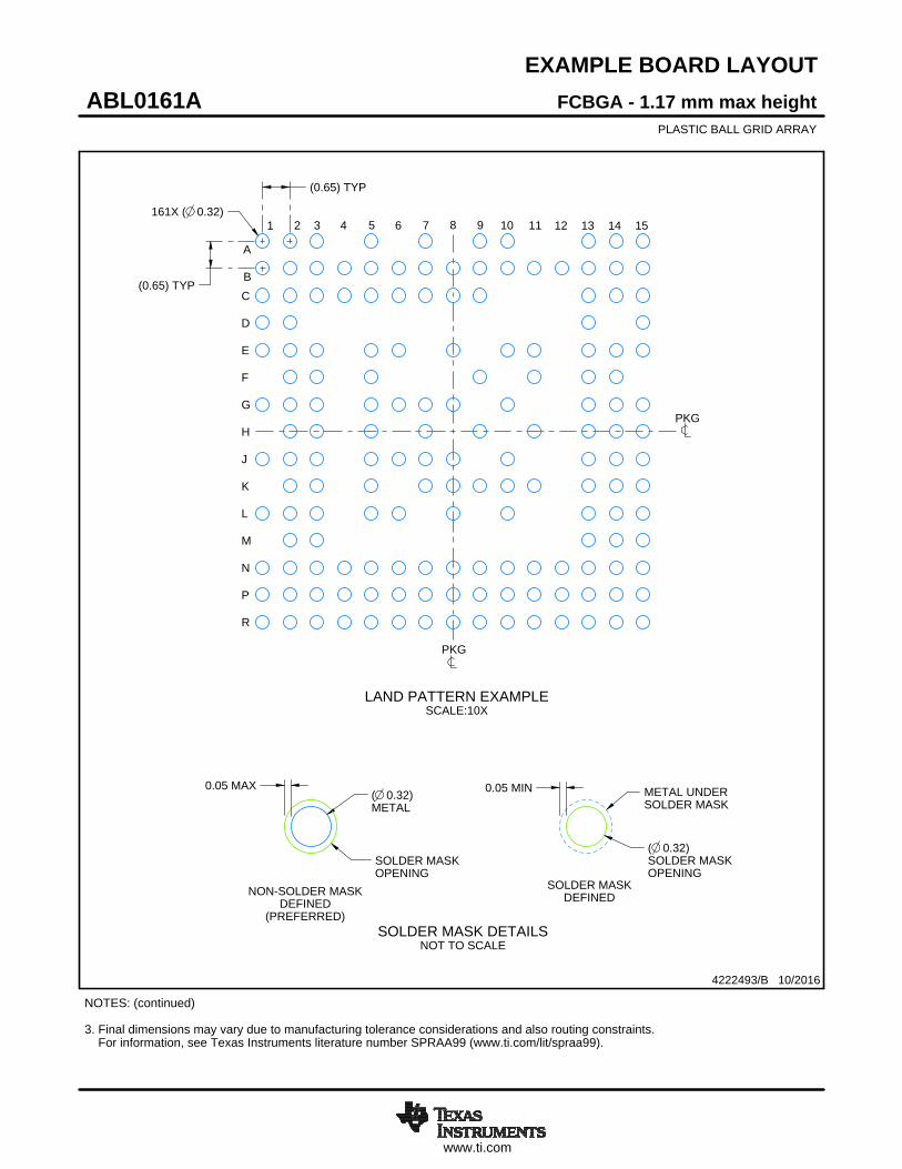
EXAMPLE BOARD LAYOUT

161X ( 0.32)

(0.65) TYP

(0.65) TYP

( 0.32)METAL

0.05 MAX

SOLDER MASKOPENING

METAL UNDERSOLDER MASK

( 0.32)SOLDER MASKOPENING

0.05 MIN

FCBGA - 1.17 mm max heightABL0161APLASTIC BALL GRID ARRAY

4222493/B 10/2016

NOTES: (continued) 3. Final dimensions may vary due to manufacturing tolerance considerations and also routing constraints. For information, see Texas Instruments literature number SPRAA99 (www.ti.com/lit/spraa99).

PKG

PKG

LAND PATTERN EXAMPLESCALE:10X

1 2 3 4 5 6 7 8 9 10 11

A

C

D

E

F

G

H

J

K

L

M

N

P

R

B

12 13 14 15

NON-SOLDER MASKDEFINED

(PREFERRED)SOLDER MASK DETAILS

NOT TO SCALE

SOLDER MASKDEFINED

www.ti.com

EXAMPLE STENCIL DESIGN

(0.65) TYP

161X ( 0.32)

(0.65) TYP

FCBGA - 1.17 mm max heightABL0161APLASTIC BALL GRID ARRAY

4222493/B 10/2016

NOTES: (continued) 4. Laser cutting apertures with trapezoidal walls and rounded corners may offer better paste release.

SOLDER PASTE EXAMPLEBASED ON 0.125 mm THICK STENCIL

SCALE:10X

PKG

PKG

1 2 3 4 5 6 7 8 9 10 11

A

C

D

E

F

G

H

J

K

L

M

N

P

R

B

12 13 14 15

PACKAGE OPTION ADDENDUM

www.ti.com 21-Jul-2018

Addendum-Page 1

PACKAGING INFORMATION

Orderable Device Status(1)

Package Type PackageDrawing

Pins PackageQty

Eco Plan(2)

Lead/Ball Finish(6)

MSL Peak Temp(3)

Op Temp (°C) Device Marking(4/5)

Samples

X1243BIGABL ACTIVE FC/CSP ABL 161 1 TBD Call TI Call TI -40 to 125

(1) The marketing status values are defined as follows:ACTIVE: Product device recommended for new designs.LIFEBUY: TI has announced that the device will be discontinued, and a lifetime-buy period is in effect.NRND: Not recommended for new designs. Device is in production to support existing customers, but TI does not recommend using this part in a new design.PREVIEW: Device has been announced but is not in production. Samples may or may not be available.OBSOLETE: TI has discontinued the production of the device.

(2) RoHS: TI defines "RoHS" to mean semiconductor products that are compliant with the current EU RoHS requirements for all 10 RoHS substances, including the requirement that RoHS substancedo not exceed 0.1% by weight in homogeneous materials. Where designed to be soldered at high temperatures, "RoHS" products are suitable for use in specified lead-free processes. TI mayreference these types of products as "Pb-Free".RoHS Exempt: TI defines "RoHS Exempt" to mean products that contain lead but are compliant with EU RoHS pursuant to a specific EU RoHS exemption.Green: TI defines "Green" to mean the content of Chlorine (Cl) and Bromine (Br) based flame retardants meet JS709B low halogen requirements of <=1000ppm threshold. Antimony trioxide basedflame retardants must also meet the <=1000ppm threshold requirement.

(3) MSL, Peak Temp. - The Moisture Sensitivity Level rating according to the JEDEC industry standard classifications, and peak solder temperature.

(4) There may be additional marking, which relates to the logo, the lot trace code information, or the environmental category on the device.

(5) Multiple Device Markings will be inside parentheses. Only one Device Marking contained in parentheses and separated by a "~" will appear on a device. If a line is indented then it is a continuationof the previous line and the two combined represent the entire Device Marking for that device.

(6) Lead/Ball Finish - Orderable Devices may have multiple material finish options. Finish options are separated by a vertical ruled line. Lead/Ball Finish values may wrap to two lines if the finishvalue exceeds the maximum column width.

Important Information and Disclaimer:The information provided on this page represents TI's knowledge and belief as of the date that it is provided. TI bases its knowledge and belief on informationprovided by third parties, and makes no representation or warranty as to the accuracy of such information. Efforts are underway to better integrate information from third parties. TI has taken andcontinues to take reasonable steps to provide representative and accurate information but may not have conducted destructive testing or chemical analysis on incoming materials and chemicals.TI and TI suppliers consider certain information to be proprietary, and thus CAS numbers and other limited information may not be available for release.

In no event shall TI's liability arising out of such information exceed the total purchase price of the TI part(s) at issue in this document sold by TI to Customer on an annual basis.

IMPORTANT NOTICE

Texas Instruments Incorporated (TI) reserves the right to make corrections, enhancements, improvements and other changes to itssemiconductor products and services per JESD46, latest issue, and to discontinue any product or service per JESD48, latest issue. Buyersshould obtain the latest relevant information before placing orders and should verify that such information is current and complete.TI’s published terms of sale for semiconductor products (http://www.ti.com/sc/docs/stdterms.htm) apply to the sale of packaged integratedcircuit products that TI has qualified and released to market. Additional terms may apply to the use or sale of other types of TI products andservices.Reproduction of significant portions of TI information in TI data sheets is permissible only if reproduction is without alteration and isaccompanied by all associated warranties, conditions, limitations, and notices. TI is not responsible or liable for such reproduceddocumentation. Information of third parties may be subject to additional restrictions. Resale of TI products or services with statementsdifferent from or beyond the parameters stated by TI for that product or service voids all express and any implied warranties for theassociated TI product or service and is an unfair and deceptive business practice. TI is not responsible or liable for any such statements.Buyers and others who are developing systems that incorporate TI products (collectively, “Designers”) understand and agree that Designersremain responsible for using their independent analysis, evaluation and judgment in designing their applications and that Designers havefull and exclusive responsibility to assure the safety of Designers' applications and compliance of their applications (and of all TI productsused in or for Designers’ applications) with all applicable regulations, laws and other applicable requirements. Designer represents that, withrespect to their applications, Designer has all the necessary expertise to create and implement safeguards that (1) anticipate dangerousconsequences of failures, (2) monitor failures and their consequences, and (3) lessen the likelihood of failures that might cause harm andtake appropriate actions. Designer agrees that prior to using or distributing any applications that include TI products, Designer willthoroughly test such applications and the functionality of such TI products as used in such applications.TI’s provision of technical, application or other design advice, quality characterization, reliability data or other services or information,including, but not limited to, reference designs and materials relating to evaluation modules, (collectively, “TI Resources”) are intended toassist designers who are developing applications that incorporate TI products; by downloading, accessing or using TI Resources in anyway, Designer (individually or, if Designer is acting on behalf of a company, Designer’s company) agrees to use any particular TI Resourcesolely for this purpose and subject to the terms of this Notice.TI’s provision of TI Resources does not expand or otherwise alter TI’s applicable published warranties or warranty disclaimers for TIproducts, and no additional obligations or liabilities arise from TI providing such TI Resources. TI reserves the right to make corrections,enhancements, improvements and other changes to its TI Resources. TI has not conducted any testing other than that specificallydescribed in the published documentation for a particular TI Resource.Designer is authorized to use, copy and modify any individual TI Resource only in connection with the development of applications thatinclude the TI product(s) identified in such TI Resource. NO OTHER LICENSE, EXPRESS OR IMPLIED, BY ESTOPPEL OR OTHERWISETO ANY OTHER TI INTELLECTUAL PROPERTY RIGHT, AND NO LICENSE TO ANY TECHNOLOGY OR INTELLECTUAL PROPERTYRIGHT OF TI OR ANY THIRD PARTY IS GRANTED HEREIN, including but not limited to any patent right, copyright, mask work right, orother intellectual property right relating to any combination, machine, or process in which TI products or services are used. Informationregarding or referencing third-party products or services does not constitute a license to use such products or services, or a warranty orendorsement thereof. Use of TI Resources may require a license from a third party under the patents or other intellectual property of thethird party, or a license from TI under the patents or other intellectual property of TI.TI RESOURCES ARE PROVIDED “AS IS” AND WITH ALL FAULTS. TI DISCLAIMS ALL OTHER WARRANTIES ORREPRESENTATIONS, EXPRESS OR IMPLIED, REGARDING RESOURCES OR USE THEREOF, INCLUDING BUT NOT LIMITED TOACCURACY OR COMPLETENESS, TITLE, ANY EPIDEMIC FAILURE WARRANTY AND ANY IMPLIED WARRANTIES OFMERCHANTABILITY, FITNESS FOR A PARTICULAR PURPOSE, AND NON-INFRINGEMENT OF ANY THIRD PARTY INTELLECTUALPROPERTY RIGHTS. TI SHALL NOT BE LIABLE FOR AND SHALL NOT DEFEND OR INDEMNIFY DESIGNER AGAINST ANY CLAIM,INCLUDING BUT NOT LIMITED TO ANY INFRINGEMENT CLAIM THAT RELATES TO OR IS BASED ON ANY COMBINATION OFPRODUCTS EVEN IF DESCRIBED IN TI RESOURCES OR OTHERWISE. IN NO EVENT SHALL TI BE LIABLE FOR ANY ACTUAL,DIRECT, SPECIAL, COLLATERAL, INDIRECT, PUNITIVE, INCIDENTAL, CONSEQUENTIAL OR EXEMPLARY DAMAGES INCONNECTION WITH OR ARISING OUT OF TI RESOURCES OR USE THEREOF, AND REGARDLESS OF WHETHER TI HAS BEENADVISED OF THE POSSIBILITY OF SUCH DAMAGES.Unless TI has explicitly designated an individual product as meeting the requirements of a particular industry standard (e.g., ISO/TS 16949and ISO 26262), TI is not responsible for any failure to meet such industry standard requirements.Where TI specifically promotes products as facilitating functional safety or as compliant with industry functional safety standards, suchproducts are intended to help enable customers to design and create their own applications that meet applicable functional safety standardsand requirements. Using products in an application does not by itself establish any safety features in the application. Designers mustensure compliance with safety-related requirements and standards applicable to their applications. Designer may not use any TI products inlife-critical medical equipment unless authorized officers of the parties have executed a special contract specifically governing such use.Life-critical medical equipment is medical equipment where failure of such equipment would cause serious bodily injury or death (e.g., lifesupport, pacemakers, defibrillators, heart pumps, neurostimulators, and implantables). Such equipment includes, without limitation, allmedical devices identified by the U.S. Food and Drug Administration as Class III devices and equivalent classifications outside the U.S.TI may expressly designate certain products as completing a particular qualification (e.g., Q100, Military Grade, or Enhanced Product).Designers agree that it has the necessary expertise to select the product with the appropriate qualification designation for their applicationsand that proper product selection is at Designers’ own risk. Designers are solely responsible for compliance with all legal and regulatoryrequirements in connection with such selection.Designer will fully indemnify TI and its representatives against any damages, costs, losses, and/or liabilities arising out of Designer’s non-compliance with the terms and provisions of this Notice.

Mailing Address: Texas Instruments, Post Office Box 655303, Dallas, Texas 75265Copyright © 2018, Texas Instruments Incorporated

Mouser Electronics

Authorized Distributor

Click to View Pricing, Inventory, Delivery & Lifecycle Information: Texas Instruments:

  X1243BIGABL


Recommended