65
BEAM SHAPING BY OPTICAL MAP TRANSFORMS Manisha Singh Master Thesis May 2012 Department of physics and mathematics University of Eastern Finland

BEAM SHAPING BY OPTICAL
MAP TRANSFORMS
Manisha Singh
Master Thesis
May 2012
Department of physics and mathematics
University of Eastern Finland
Manisha Singh Beam shaping by optical map transform , 55 pages
University of Eastern Finland
Msc. in Photonics
Instructors Prof. Jari Turunen
Docent Jani Tervo
Abstract
This work contains theoretical, numerical, and experimental studies on laser beam
shaping. The basic concepts of wave optical analysis of propagation of optical fields
and the scalar theory of diffraction are discussed, and applied to the design of diffrac-
tive beam shaping elements which transform a Gaussian beam into a uniform irradi-
ance profile in the Fresnel domain or in far field. Fabrication and characterization
of these elements is also considered. Conclusions are made on the choice of design,
depending on the tolerances available.

Preface
My interest to become an optical designer in future led to my interest in diffractive
optics which finally encouraged to this thesis. During these time I have experienced
a lot from theory to its application. Many of these ideas originated as a result of
brainstorming discussion in ACTMOST project.
I am really grateful to my supervisor, Prof. Jari Turunen and Docent Jani Tervo,
who have guided me and shown their confidence in me. I will always be indebted to
their constant help and for increasing a self confidence in me. I also want to thank
Prof. Pasi Vahimaa, the head of our department and i would like to offer my special
thanks to Faculty of Forestry and Sciences for providing financial support during
my Masters studies.
This thesis would not have been possible without the co-operation and kind help of
my supervisors, Janne Laukkanen, Pertti Paakkonen, Tommi Itkonen, and members
of technical and electrical workshop.
Finally, my warmest thanks goes to my parents and friends who have encouraged
and supported me during these years.
Joensuu, May 2012
Manisha Singh
iii
Contents
1 Introduction 1
2 Aim and scope 3
3 Free-space propagation of optical fields 7
3.1 Introduction . . . . . . . . . . . . . . . . . . . . . . . . . . . . . . . . 7
3.2 Angular spectrum representation . . . . . . . . . . . . . . . . . . . . 7
3.3 Rayleigh-Sommerfeld propagation . . . . . . . . . . . . . . . . . . . . 9
3.4 Fresnel diffraction . . . . . . . . . . . . . . . . . . . . . . . . . . . . . 10
3.5 Fast Fourier Transformation algorithm (FFT) . . . . . . . . . . . . . 11
3.6 Complex amplitude transmittance approach (CATA) . . . . . . . . . 12
3.7 Gaussian beams . . . . . . . . . . . . . . . . . . . . . . . . . . . . . . 13
4 Optical map transform 15
4.1 Design examples . . . . . . . . . . . . . . . . . . . . . . . . . . . . . 17
4.1.1 Paraxial beam shaping case . . . . . . . . . . . . . . . . . . . 17
4.1.2 Far-field beam shaping case . . . . . . . . . . . . . . . . . . . 23
5 Tolerance analysis 30
5.1 Near-Field: Lateral and longitudinal displacement . . . . . . . . . . . 30
5.2 Far-field: Lateral and longitudinal displacement . . . . . . . . . . . . 33
iv

6 Characterization and fabrication errors 37
6.1 Simulation . . . . . . . . . . . . . . . . . . . . . . . . . . . . . . . . . 37
6.2 Fabrication . . . . . . . . . . . . . . . . . . . . . . . . . . . . . . . . 38
6.2.1 Effect of etch depth error . . . . . . . . . . . . . . . . . . . . . 43
6.3 Characterization . . . . . . . . . . . . . . . . . . . . . . . . . . . . . 47
6.3.1 Fresnel domain . . . . . . . . . . . . . . . . . . . . . . . . . . 48
6.3.2 Far-field . . . . . . . . . . . . . . . . . . . . . . . . . . . . . . 51
7 Conclusion 54
8 Future-work 56
Bibliography 57
v
Chapter I
Introduction
Beam shaping started back in seventh century B.C with the use of magnifying glass
to concentrate sunlight to burn wood [1]. For about 180 years, use of Fresnel lenses
[2, 3] in light houses, traffic lights, wireless networks, and overhead projectors have
been some of the important beam shaping applications. Beam shaping has been used
for improving technologies like lithography [4], laser printing [5], some medicine and
laboratory research [5], material processing [6], micro machining, laser processing [7],
line integrator [8], camera optics [8], and holography [9].
Beam shaping methods can be divided in two groups. First, there are beam
integrators in which the input beam is split into separate components and merged
at target plane to get a desired profile [7]. The second approach to beam shaping,
to be considered in this thesis, is based on geometrical map transforms. A beam
transformer performs field mapping from input to target plane [10–12]. For example,
transformation of Gaussian beam into top-hat [13], super-Gaussian, Bessel [14],
Fermi-Dirac, or some other shape with specified irradiance [15] can be of interest.
Beam transformers can be based on refractive [16], reflective or diffractive optics [17].
This thesis mainly focuses on diffractive optics.
One of the first beam-shaping papers was published by Frieden in 1965 [18] and
a device using map-transform techniques was introduced by Han in 1983 [19]. It
converted a Gaussian beam into a uniform irradiance distribution by use of two
consecutive elements. Later, rotationally symmetric and one dimensional axicons
[20–22] and beam-shaping elements for lasers [13,23–29] were designed using a single
element.
This thesis concerns the design, tolerance analysis, fabrication, and characteri-
1
zation of beam shaping elements based on geometrical map transforms. This work
is partially theoretical and partially experimental. Chapter II deals with the scope
of the thesis and chapter III deals with fundamentals of diffraction and scalar wave
theory. In chapter IV, methods for analysis of propagation of optical fields are
considered for uniform medium. The paraxial approximation case like Fresnel prop-
agation formula and the complex amplitude transmittance approach method are also
discussed. Chapter V deals with design examples and theoretical simulation results
on diffractive beam shaping elements. Design, optimization, and tolerance analysis
are discussed in chapter VI. Finally, conclusions are drawn in chapter VII and some
prospects for future work are outlined in chapter VIII.
2

Chapter II
Aim and scope
Transforming a Gaussian beam to one with uniform irradiance is important for
many applications: for example laser material processing, laser scanning, and laser
radar [7] require uniform irradiance with desired shape and sharp edges. The beam
properties at a given distance z from the initial plane are completely determined by
the beam properties at the initial plane. Usually one is interested in the intensity
distribution at a given target plane. Then the question arises: how can a desired
intensity distribution in the plane z or at a some other surface be produced only by
choosing the beam properties at the initial plane?
The aim of this thesis is to use diffractive optics to convert a known input field
or beam into one with defined output distribution. In practise, the most important
example is converting a Gaussian input beam to flat top beam. The approach
adopted here is based on the geometrical map transform technique. The concept is
old, but realization of the required diffractive elements at high light efficiency has
become possible much more recently, as a result of developments in lithographic
fabrication techniques of phase-modulating elements [36].
The beam shaping diffractive elements perform a 1-to-1 mapping of the input
light to output profile, and we can control both intensity and phase of the output
beam. Designing the phase function of beam shaping element is done using map
transform method in Matlab.
Some critical factors like fabrication errors and alignment issues were considered
as they affect the performance of these beam shaping elements.
Within scalar theory the desired complex amplitude transmittance function of
the element may be calculated by propagating the field from the signal plane to the
3
element plane and dividing by the incident beam. The resulting element is then
characterized by continuous amplitude and phase modulation. Usually one prefers
phase only modulation, because it is easier to produce elements that modulate only
the phase rather than the phase and amplitude. It is always possible to modulate
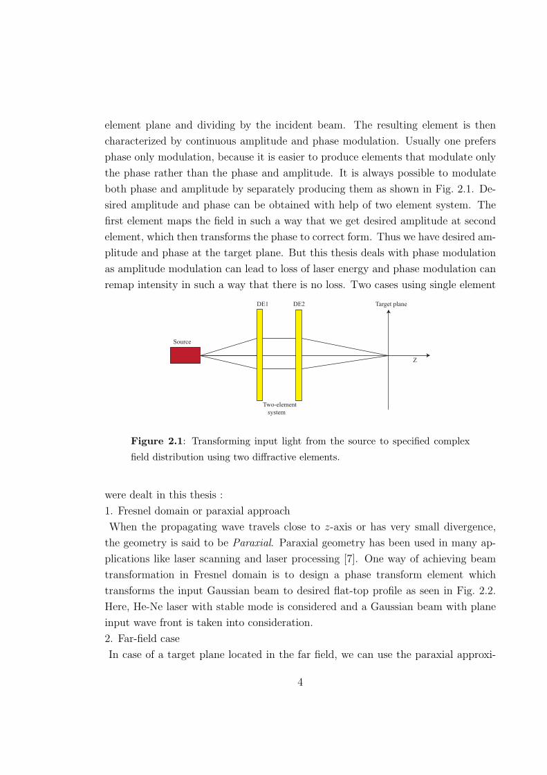
both phase and amplitude by separately producing them as shown in Fig. 2.1. De-
sired amplitude and phase can be obtained with help of two element system. The
first element maps the field in such a way that we get desired amplitude at second
element, which then transforms the phase to correct form. Thus we have desired am-
plitude and phase at the target plane. But this thesis deals with phase modulation
as amplitude modulation can lead to loss of laser energy and phase modulation can
remap intensity in such a way that there is no loss. Two cases using single element
Source
DE1 DE2 Target plane
Z
Two-element
system
Figure 2.1: Transforming input light from the source to specified complex
field distribution using two diffractive elements.
were dealt in this thesis :
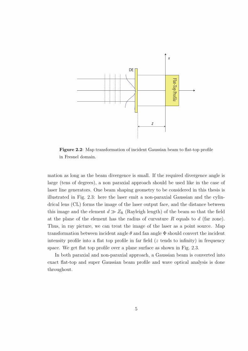
1. Fresnel domain or paraxial approach
When the propagating wave travels close to z-axis or has very small divergence,
the geometry is said to be Paraxial. Paraxial geometry has been used in many ap-
plications like laser scanning and laser processing [7]. One way of achieving beam
transformation in Fresnel domain is to design a phase transform element which
transforms the input Gaussian beam to desired flat-top profile as seen in Fig. 2.2.
Here, He-Ne laser with stable mode is considered and a Gaussian beam with plane
input wave front is taken into consideration.
2. Far-field case
In case of a target plane located in the far field, we can use the paraxial approxi-
4
x
DE
z
Flat-Top Profile
Figure 2.2: Map transformation of incident Gaussian beam to flat-top profile
in Fresnel domain.
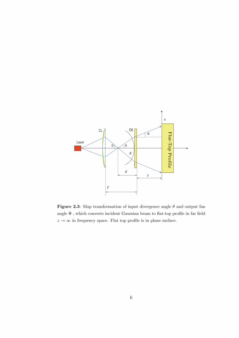
mation as long as the beam divergence is small. If the required divergence angle is
large (tens of degrees), a non paraxial approach should be used like in the case of
laser line generators. One beam shaping geometry to be considered in this thesis is
illustrated in Fig. 2.3: here the laser emit a non-paraxial Gaussian and the cylin-
drical lens (CL) forms the image of the laser output face, and the distance between
this image and the element d ≫ ZR (Rayleigh length) of the beam so that the field
at the plane of the element has the radius of curvature R equals to d (far zone).
Thus, in ray picture, we can treat the image of the laser as a point source. Map
transformation between incident angle θ and fan angle Φ should convert the incident
intensity profile into a flat top profile in far field (z tends to infinity) in frequency
space. We get flat top profile over a plane surface as shown in Fig. 2.3.
In both paraxial and non-paraxial approach, a Gaussian beam is converted into
exact flat-top and super Gaussian beam profile and wave optical analysis is done
throughout.
5
Laser
x
DECL
d
Φ
θ
F
Fla
t-To
p P
rofile
θ
z
R
Figure 2.3: Map transformation of input divergence angle θ and output fan
angle Φ , which converts incident Gaussian beam to flat-top profile in far field
z → ∞ in frequency space. Flat top profile is in plane surface.
6

Chapter III
Free-space propagation of optical fields
3.1 Introduction
Maxwell’s equations [31] form the basis for considering propagation of any electro-
magnetic field. When we talk about wavelength scale feature size for diffractive
element, an accurate analysis of the element requires that the light is treated as
an electromagnetic wave. Here, however it sufficient to consider scalar theory of
electromagnetic field which ignores polarization effects.
One characteristic of Maxwell’s equations is that every Cartesian component
U(x, y, z) of the electric field in space-frequency domain obeys well known Helmholtz
wave Eq.(3.1).
∇2U(x, y, z) + k2U(x, y, z) = 0, (3.1)
where k = 2π/λ is the wavenumber and λ is the wavelength of light. The simplest
solution of Eq.( 3.1)is a harmonic plane wave.
U(x, y, z) = Uoei(kxx+kyy+kzz) (3.2)
where Uo is complex constant, ω is the angular frequency of the wave, and k =
(kx, ky, kz) is the wave vector. Here stationary fields are taken into consideration,
and hence we assume |U | is time independent.
3.2 Angular spectrum representation
The angular spectrum representation is a mathematical technique to describe how
the field propagates over a certain distance. Here we consider propagation in free
7
space. The approach is to calculate the Fourier transform of the Helmholtz Eq.( 3.1)
with respect to x and y yielding
d2
dz2U(u, v, z) + 4π2β2U(u, v, z) = 0, (3.3)
where
β2 =
(k
2π
)2
− (u2 + v2) (3.4)
and the Fourier transform is defined here as
U(u, v, z) =
(1
2π
)2 ∫∫ ∞
−∞U(x, y, z)e−i2π(ux+vy)dxdy. (3.5)
The general solution of this second order differential is
U(u, v, z) = T (u, v)ei2πβz +R(u, v)e−i2πβz (3.6)
from which the solution of Eq.( 3.1) can be found by the inverse Fourier transform
U(u, v, z) =
∫∫ ∞
−∞T (u, v)ei2π(ux+vy+βz)dudv +
∫∫ ∞
−∞R(u, v)ei2π(ux+vy−βz)dudv.
(3.7)
The term T describes waves propagating in positive z direction and R describes
the backward propagating waves. Propagation factor β of Eq.( 3.4) can be either
real or an imaginary depending on the magnitude of u2 + v2. A real propagation
factor describes plane waves according to Eq.( 3.2) and imaginary propagation factor
denotes exponentially increasing or decreasing waves. The representation (3.7) is
called Plane Wave Decomposition of an optical field.
If we consider only half space z ≥ 0, and sources in z < 0, we can ignore
exponentially increasing and backward propagating waves by writing R(u, v) = 0.
Now Eq.( 3.6) describes an infinite number of plane waves propagating in directions
defined by u and v. Now if we consider our reference plane at z = 0, then the
propagation problem can be formulated as
U(u, v, z) =
∫∫ ∞
−∞T (u, v)ei2π(ux+vy+βz)dudv (3.8)
where
T (u, v) =
(1
2π
)2 ∫∫ ∞
−∞U(x′, y′, 0)e−i2π(ux′+vy′)dx′dy′ (3.9)
8
where x′ and y′ denote the position coordinates at the plane z = 0.
Equation ( 3.8) is the Angular Spectrum Representation of the field and the
quantity T (u, v) in Eq. (3.9) is called the complex angular spectrum of the field at
z = 0. Since we have not used any approximation, this propagation method is exact
in terms of scalar theory. The integrals in Eq. (3.8) and (3.9) can be evaluated
numerically using direct and inverse Fast Fourier Transforms (FFT).
The above given equations for angular spectrum representation for scalar fields
can also be extended to electromagnetic vector fields. Angular spectrum formulas
(3.8)-(3.9) can be applied to electric field components Ex and Ey independently and
then Ez can be solved.
3.3 Rayleigh-Sommerfeld propagation
The angular spectrum representation defined by Eqs. (3.8)-(3.9) can be re-written
with slightly different notation as
U(u, v, z) =
∫∫ ∞
−∞T (p, q)eik(px+qy+mz)dpdq (3.10)
and
T (u, v) =
(k
2π
)2 ∫∫ ∞
−∞U(x′, y′, 0)(e−ik(px′+qy′)dx′dy′, (3.11)
where p = λu, q = λv and
m2 = 1− (p2 + q2). (3.12)
A combination of Eq.(3.10)-Eq.(3.11) yields
U(x, y, z) =
∫∫ ∞
−∞U(x′, y′)G(x− x′, y − y′, z)dx′dy′, (3.13)
where
G(x− x′, y − y′, z)) =
(k
2π
)2 ∫∫ ∞
−∞eik[p(x−x′)+q(y−y′)+mz]dpdq (3.14)
is the Green function of the propagation problem [33]. Denoting r = (x, y, z) and
r′ = (x′, y′, 0) and using the Weyl representation of spherical wave [33]
eik|r−r′|
|r− r′|=
(ik
2π
)2 ∫∫ ∞
−∞
1
me−ik[p(x−x′)+q(y−y′)+mz]dpdq (3.15)
9
the Green function Eq. (3.15) can be represented as
G(x− x′, y − y′, z) = − 1
2π
∂
∂z
(1
ReikR
), (3.16)
where
R =| r − r′ |=√
(x− x′)2 + (y − y′)2 + z2. (3.17)
Thus the Green function is
G(x− x′, y − y′, z) = − 1
2π
(ik − 1
ReikR
)z
R2eikR (3.18)
and substitution into Eq. (3.13) gives
U(x, y, z) = − z
2π
∫∫ ∞
−∞U(x′, y′, 0)
(ik − 1
ReikR
)1
R2eikRdx′dy′, (3.19)
which is known as Rayleigh-Sommerfeld Diffraction Formula. This propagation
method is exact in sense of scalar theory but has a singularity at propagation dis-
tance z = 0. Thus Rayleigh-Sommerfeld diffraction formula cannot be used for short
distances as it will lead to numerical instability.
Rayleigh-Sommerfeld diffraction formula here was derived by angular spectrum
representation but it can be derived in many other ways, like starting from Huygen’s
principle.
3.4 Fresnel diffraction
When the propagating wave travels close to z-axis or has very small divergence, the
geometry is said to be paraxial. Then MacLaurin expansion of R,
R ≈ z +1
2z
[(x− x′)2 + (y − y′)2
](3.20)
can be used in the exponential term of Rayleigh-Sommerfeld diffraction formula
(3.19) and one can write R ≈ z in the denominator. The resulting approximate
propagation formula is
U(x, y, z) = − ik
2πzeikz
∫∫ ∞
−∞U(x′, y′, 0)eik[(x−x′)2+(y−y′)2]/2zdx′dy′ (3.21)
is called Fresnel diffraction formula. It can also be derived directly from the an-
gular spectrum representation Eq. (3.10)-(3.11) without using Rayleigh Sommerfeld
10
diffraction formula. The Fresnel propagation integral is a widely used formula for
beam-like wave propagation. With this diffraction formula, several analytical results
can be achieved in closed form unlike from the Rayleigh-Sommerfeld diffraction for-
mula. This advantage could be seen in cases like propagation conditions for Gaus-
sian beams where distance between the source and element is greater than Rayleigh
length
d >> zr
and plane of the element has radius curvature R equal to d in far zone. When the
square in the exponential is expanded, the phase factor
(x′2 + y′2)
appears and if it is small it can be ignored. And resulting equation is Fraunhofer
propagation formula which is a good approximation in far-field.
3.5 Fast Fourier Transformation algorithm (FFT)
The FFT algorithm can be used for all three above mentioned propagation meth-
ods: angular spectrum representation, Rayleigh-Sommerfield diffraction and Fresnel
diffraction formula. It reduces the numerical computational time. Equations (3.13)
and (3.21) are actually convolutions of two functions
(U ∗G)(x, y) =
∫∫ ∞
−∞U(x′, y′)G(x− x′, y − y′, z)dx′dy′, (3.22)
each of them having different Green Function G. Thus, from the property of convo-
lutions,
F {U ∗G} = F {U}F {G} . (3.23)
The Fourier transform of the final field U(x, y, z) is the product of the Fourier
transforms of the initial field U(x′, y′, 0) and the Green function G(x− x′, y − y′, z)
associated with the propagation problem. Due to inherent periodicity of FFT al-
gorithm, it is very useful for analyzing periodic fields. For non-periodic fields zero
padding should be done in element plane.
11
3.6 Complex amplitude transmittance approach (CATA)
This approach treats the diffractive element as a thin screen that modulates the
amplitude, phase, and sometimes also the polarization properties of the incident
field. We can use this method, when the thickness of the grating profile is of the
order of wavelength and minimum feature size is larger than 10λ, otherwise rigorous
grating analysis methods such as the Fourier Modal Method (FMM) [34,35] should
be used. CATA can also be used for the analysis of non-periodic structures.
Complex amplitude transmittance approach states that the scalar incident field
Ui(x, 0) and the transmitted field Ut(x, t) are related to each other as
Ut(x, t) = t(x)Ui(x, 0), (3.24)
where t(x) is the complex amplitude transmission function and t is the thickness of
the element. The complex refractive index is defined as
n(x, z) = n(x, z) + iκ(x, z), (3.25)
where n(x, z) is the real refractive index and κ(x, z) is the absorbtion coefficient. If
the thickness t is small, it can be said that the propagating wave is affected only
by point wise amplitude and phase change. If the area is fully transparent or non
conductive, i.e., κ = 0, the element only affects the phase of the incident field (phase
only element). The function t(x) can then be determined by calculating optical path
at each point of the element:
t(x) = exp
[ik
∫ t
0
n(x, z)dz
]. (3.26)
In this thesis only phase only diffractive elementss are considered. For a periodic
structure the complex amplitude transmission function can be expressed in Fourier
expansion as
t(x) =∞∑
m=−∞
Tm exp
(i2πmx
d
), (3.27)
where the Fourier coefficients Tm are obtained from
T (m) =1
d
∫ d
0
t(x) exp
(−i2πmx
d
)dx, (3.28)
12
where d is the grating period and m is the diffraction order. Diffraction efficiency
of mth diffraction orders is given by
ηm = |Tm|2 (3.29)
if we ignore Fresnel reflection losses.
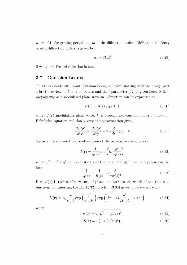
3.7 Gaussian beams
This thesis deals with input Gaussian beam, so before starting with the design part
a brief overview on Gaussian beams and their parameter [32] is given here. A field
propagating as a modulated plane wave in z direction can be expressed as,
U(r) = A(r) exp(ikz), (3.30)
where A(r) modulating plane wave, k is propagation constant along z direction.
Helmholtz equation and slowly varying approximation gives,
d2A(r)
d2x+
d2A(r)
d2y− 2ik
d
dzA(r) = 0. (3.31)
Gaussian beams are the one of solution of the paraxial wave equation,
A(r) =A1
q(z)exp
(ik
ρ2
2q(z)
), (3.32)
where ρ2 = x2 + y2, A1 is constant and the parameter q(z) can be expressed in the
form1
q(z)=
1
R(z)− i
λ
πw(z)2. (3.33)
Here R(z) is radius of curvature of phase and w(z) is the width of the Gaussian
function. On inserting the Eq. (3.32) into Eq. (3.30) gives full wave equation,
U(r) = A0w
w(z)exp
(ρ2
w(z)2
)exp
(ikz − ik
ρ2
2R(z)− iς(z)
), (3.34)
where
w(z) = w0
√1 + (z/zR)
2, (3.35)
R(z) = z(1 + (z/zR)
2), (3.36)
13
ς(z) = tan−1 z
zR, (3.37)
w0 =
√λzRπ
, (3.38)
and
A0 =A1
izR. (3.39)
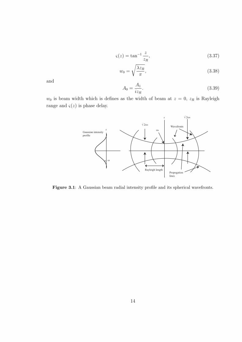
w0 is beam width which is defines as the width of beam at z = 0, zR is Rayleigh
range and ς(z) is phase delay.
rGaussian intensity profile
ω
r
Wavefronts
Propogation lines
√ 2ω0
ω0
Rayleigh length
√ 2ω0
Figure 3.1: A Gaussian beam radial intensity profile and its spherical wavefronts.
14
Chapter IV
Optical map transform
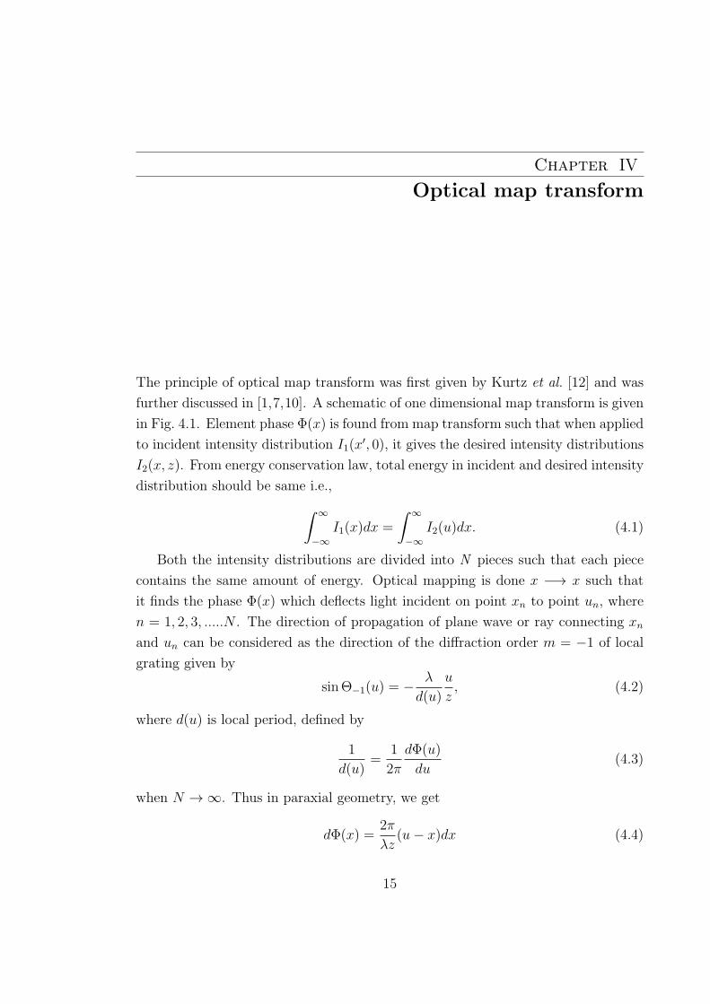
The principle of optical map transform was first given by Kurtz et al. [12] and was
further discussed in [1,7,10]. A schematic of one dimensional map transform is given
in Fig. 4.1. Element phase Φ(x) is found from map transform such that when applied
to incident intensity distribution I1(x′, 0), it gives the desired intensity distributions
I2(x, z). From energy conservation law, total energy in incident and desired intensity
distribution should be same i.e.,∫ ∞
−∞I1(x)dx =
∫ ∞
−∞I2(u)dx. (4.1)
Both the intensity distributions are divided into N pieces such that each piece
contains the same amount of energy. Optical mapping is done x −→ x such that
it finds the phase Φ(x) which deflects light incident on point xn to point un, where
n = 1, 2, 3, .....N . The direction of propagation of plane wave or ray connecting xn
and un can be considered as the direction of the diffraction order m = −1 of local
grating given by
sinΘ−1(u) = − λ
d(u)
u
z, (4.2)
where d(u) is local period, defined by
1
d(u)=
1
2π
dΦ(u)
du(4.3)
when N → ∞. Thus in paraxial geometry, we get
dΦ(x) =2π
λz(u− x)dx (4.4)
15
The mapping x −→ u can be found by integration∫ x
x0
I1(ξ′)dξ′ =
∫ u
u0
I2(ξ)dξ (4.5)
The optical map transform is a good approach for paraxial design but if the geometry
x u
1
2
3
N
N
z
z
1
2
3
z = 0
Figure 4.1: Principle of optical map transform
is not paraxial then one has to do it numerically, and elements designed by it are
sensitive to fabrication and alignment errors.
Throughout this thesis we have talked about transforming the Gaussian beam
into exact flat-top and super-Gaussian. This is because field emitted by lasers typi-
cally have Gaussian profile and we often want to transform them to uniform intensity
profile. Before starting with the design part, let us give an overview what exact flat-
top and super-Gaussian means. When we are talking about exact flat-top we mean
intensity or field distribution with sharp edges but super-Gaussian has rounded edges
and it becomes sharper with the increase in order N .
I(x) = exp
(−x
w
)N
(4.6)
16
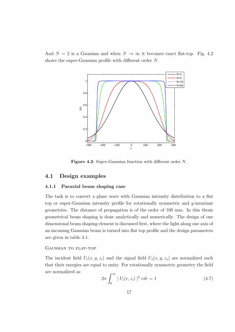
And N = 2 is a Gaussian and when N → ∞ it becomes exact flat-top. Fig. 4.2
shows the super-Gaussian profile with different order N .
−300 −200 −100 0 100 200 300
0
0.2
0.4
0.6
0.8
1
x
I(x)
N=2N=4N=16N=64
Figure 4.2: Super-Gaussian function with different order N .
4.1 Design examples
4.1.1 Paraxial beam shaping case
The task is to convert a plane wave with Gaussian intensity distribution to a flat
top or super-Gaussian intensity profile for rotationally symmetric and y-invariant
geometries. The distance of propagation is of the order of 100 mm. In this thesis
geometrical beam shaping is done analytically and numerically. The design of one
dimensional beam shaping element is discussed first, where the light along one axis of
an incoming Gaussian beam is turned into flat top profile and the design parameters
are given in table 4.1.
Gaussian to flat-top
The incident field Ui(x, y, zi) and the signal field Us(x, y, zs) are normalized such
that their energies are equal to unity. For rotationally symmetric geometry the field
are normalized as
2π
∫ ∞
0
| Ui(r, zi) |2 rdr = 1 (4.7)
17

Table 4.1: Table of specification
Parameter Value
Wavelength(nm) 633
Input beam shape Axial Symmetrical Guassian beam
Input beam waist 555 µm
Output beam shape Flat top
Propagation distance 30-100 mm
and
2π
∫ ∞
0
| Us(ρ, zs) |2 ρdρ = 1, (4.8)
where r =√(x2 + y2) and ρ =
√(u2 + v2). The energy balance condition is∫ r
0
| Ui(r′, zi) |2 r′dr′ =
∫ ρ
0
| Us(ρ′, zs) |2 ρ′dρ′ (4.9)
The normalization of the Gaussian incident field
2π
∫ ∞
−∞Ui(r
′)exp
(−2r2
w2
)rdr = 1, (4.10)
leads to
Ui = −ω2π
2. (4.11)
The flat-top field is
Us(ρ′, zs) =
{Us if |ρ| ≤ a2
0 otherwise(4.12)
and its normalization gives
|Us|2 =π
a4. (4.13)
In accordance with the map-transform principle, we divide the incident intensity
Ii(x) and the signal intensity Is(u) into N parts each containing equal amount of
energy. The DE then redirects the incident ray in such a way that light from each
part in the x-plane is directed towards corresponding part in u-plane. Now, we
consider y-invariant element geometry and energy balance condition or mapping
condition x → u(x) given in Eq. (4.14) and in Fig. 4.3:∫ x
0
| Ui(x′, zi) |2 dx′ =
∫ u(x)
0
| Us(u′, zs) |2 du′ (4.14)
18
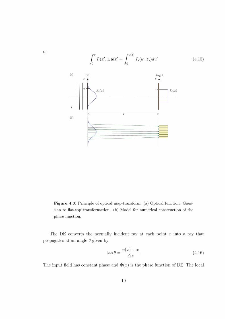
or ∫ x
0
Ii(x′, zi)dx
′ =
∫ u(x)
0
Is(u′, zs)du
′ (4.15)
x u
DE target(a)
(b)
λ
z
w aI(x’,zi) I(u,zs)
Figure 4.3: Principle of optical map-transform. (a) Optical function: Gaus-
sian to flat-top transformation. (b) Model for numerical construction of the
phase function.
The DE converts the normally incident ray at each point x into a ray that
propagates at an angle θ given by
tan θ =u(x)− x
△z. (4.16)
The input field has constant phase and Φ(x) is the phase function of DE. The local
19
ray direction is normal to the constant phase of the field just after the DE. We have
sin θ =1
k
dΦ(x)
dx(4.17)
and by integrating
Φ(x) =k
△z
∫ x
0
[u(x′)− x]dx′. (4.18)
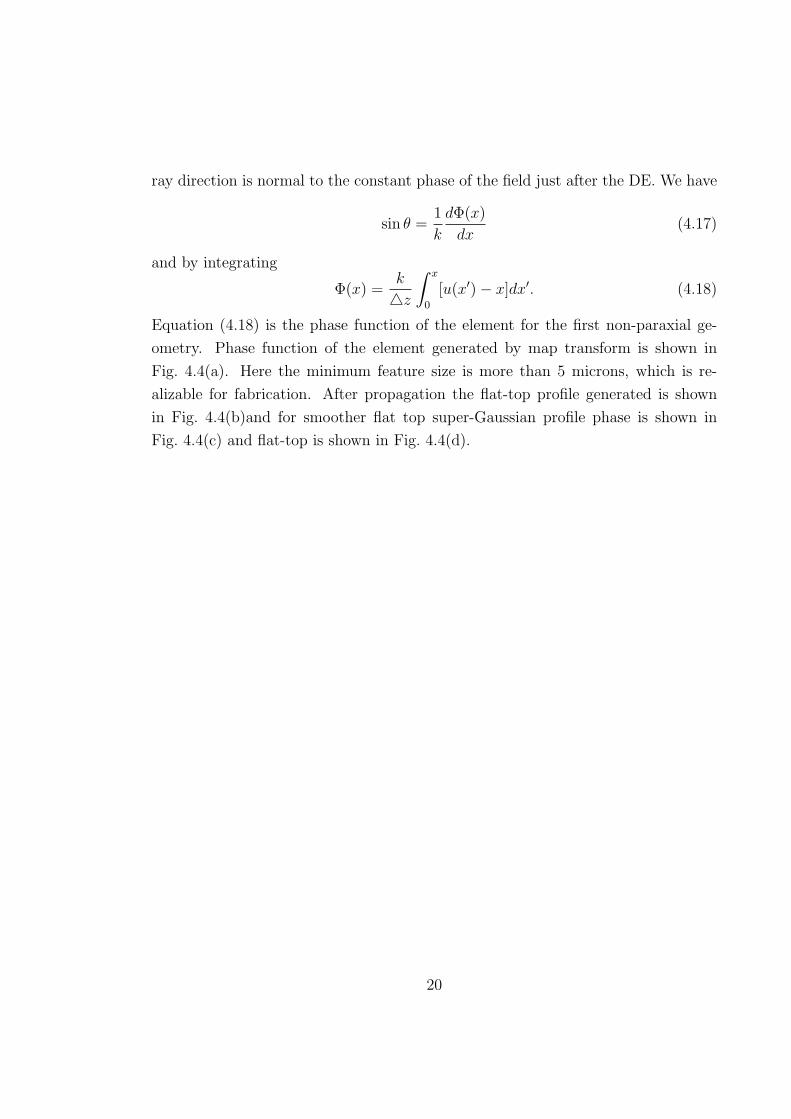
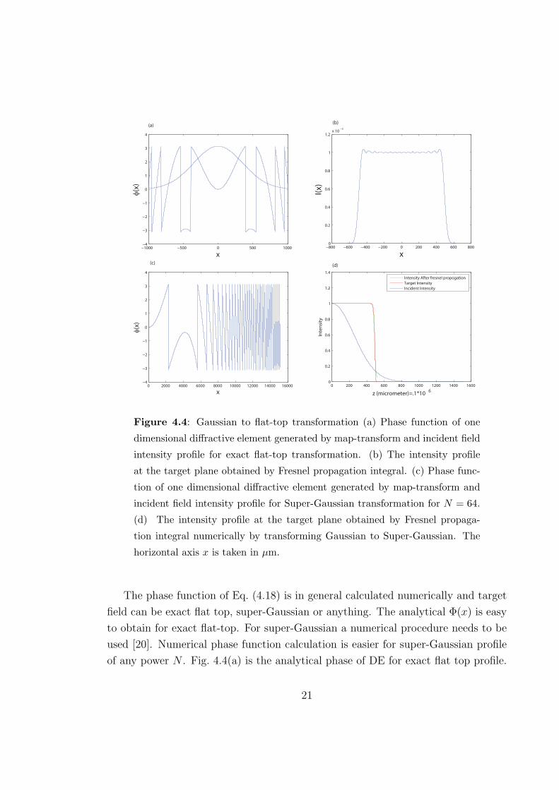
Equation (4.18) is the phase function of the element for the first non-paraxial ge-
ometry. Phase function of the element generated by map transform is shown in
Fig. 4.4(a). Here the minimum feature size is more than 5 microns, which is re-
alizable for fabrication. After propagation the flat-top profile generated is shown
in Fig. 4.4(b)and for smoother flat top super-Gaussian profile phase is shown in
Fig. 4.4(c) and flat-top is shown in Fig. 4.4(d).
20
−1000 −500 0 500 1000−4
−3
−2
−1
0
1
2
3
4
x
φ(x)
(a)
−800 −600 −400 −200 0 200 400 600 8000
0.2
0.4
0.6
0.8
1
1.2x 10
−3
x
I(x
)
(b)
0 2000 4000 6000 8000 10000 12000 14000 16000−4
−3
−2
−1
0
1
2
3
4
x
φ(x)
(c)
0 200 400 600 800 1000 1200 1400 16000
0.2
0.4
0.6
0.8
1
1.2
1.4
z (micrometer)=.1*106
Inte
nsi
ty
Intensity After fresnel propogation
Target Intensity
Incident Intensity
(d)
Figure 4.4: Gaussian to flat-top transformation (a) Phase function of one
dimensional diffractive element generated by map-transform and incident field
intensity profile for exact flat-top transformation. (b) The intensity profile
at the target plane obtained by Fresnel propagation integral. (c) Phase func-
tion of one dimensional diffractive element generated by map-transform and
incident field intensity profile for Super-Gaussian transformation for N = 64.
(d) The intensity profile at the target plane obtained by Fresnel propaga-
tion integral numerically by transforming Gaussian to Super-Gaussian. The
horizontal axis x is taken in µm.
The phase function of Eq. (4.18) is in general calculated numerically and target
field can be exact flat top, super-Gaussian or anything. The analytical Φ(x) is easy
to obtain for exact flat-top. For super-Gaussian a numerical procedure needs to be
used [20]. Numerical phase function calculation is easier for super-Gaussian profile
of any power N . Fig. 4.4(a) is the analytical phase of DE for exact flat top profile.
21
Here target distribution is I(u) = 12a
, 0 < u < a, where a is chosen to be 500 µm
and z is propagation distance. The analytical phase for Gaussian to exact flat-top
conversion is
ϕ(x) =2π
λz
(aω
−1 + exp(−2x2/ω2)√2π
− x2
2+ axerf
√2x
ω
). (4.19)
Now, with the same parameters of 1D solution, it can be crossed to get rectan-
gular flat-top profiles. For two dimensional rectangular case phase function is
Φ(x, y) = Φ(x)Φ(y) (4.20)
where both Φ(x) andΦ(y) are of the form of Eq.( 4.19). Three propagation method
namely angular spectrum representation, Rayleigh Sommerfeld diffraction and Fres-
nel diffraction were used to evaluate the quality of the flat top profile in target plane.
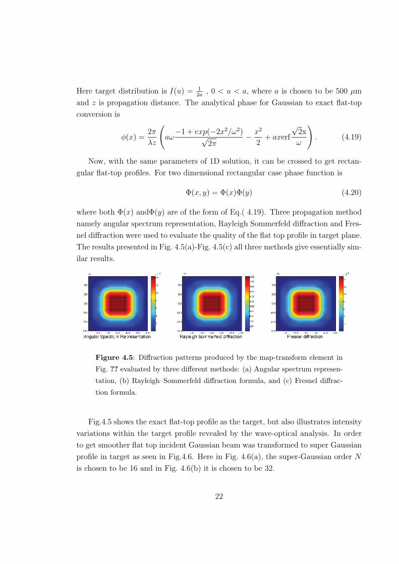
The results presented in Fig. 4.5(a)-Fig. 4.5(c) all three methods give essentially sim-
ilar results.
(a) (c) (b)
Figure 4.5: Diffraction patterns produced by the map-transform element in
Fig. ?? evaluated by three different methods: (a) Angular spectrum represen-
tation, (b) Rayleigh–Sommerfeld diffraction formula, and (c) Fresnel diffrac-
tion formula.
Fig.4.5 shows the exact flat-top profile as the target, but also illustrates intensity
variations within the target profile revealed by the wave-optical analysis. In order
to get smoother flat top incident Gaussian beam was transformed to super Gaussian
profile in target as seen in Fig.4.6. Here in Fig. 4.6(a), the super-Gaussian order N
is chosen to be 16 and in Fig. 4.6(b) it is chosen to be 32.
22
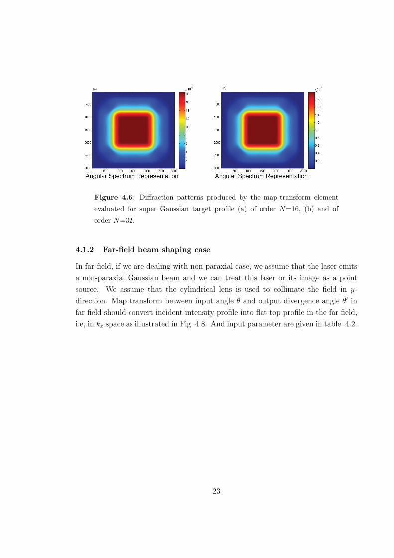
(a) (b)
Figure 4.6: Diffraction patterns produced by the map-transform element
evaluated for super Gaussian target profile (a) of order N=16, (b) and of
order N=32.
4.1.2 Far-field beam shaping case
In far-field, if we are dealing with non-paraxial case, we assume that the laser emits
a non-paraxial Gaussian beam and we can treat this laser or its image as a point
source. We assume that the cylindrical lens is used to collimate the field in y-
direction. Map transform between input angle θ and output divergence angle θ′ in
far field should convert incident intensity profile into flat top profile in the far field,
i.e, in kx space as illustrated in Fig. 4.8. And input parameter are given in table. 4.2.
23

S
z
x
DE CL
d + ∆z
S
z
y
DE CL
F
θ′ θ
adjustment
Figure 4.7: Light incident from point source to the DE and ∆z is a longi-
tudinal position error, where d is distance between the source and DE. CL is
cylindrical lens which collimates the beam in y and gives flat-top profile in x
direction.
Here incident ray at angle θ′ is transformed to into a ray at angle θ, for our far
field kx = k sin θ and maximum divergence angle Φ with kx = k sinΦ.
Table 4.2: Table of specification
Parameter Value
Wavelength(nm) 633
Distance between source and element(d) 3000 µm
Input divergence angle 100
Output divergence angle 100
Propagation distance Far field
24
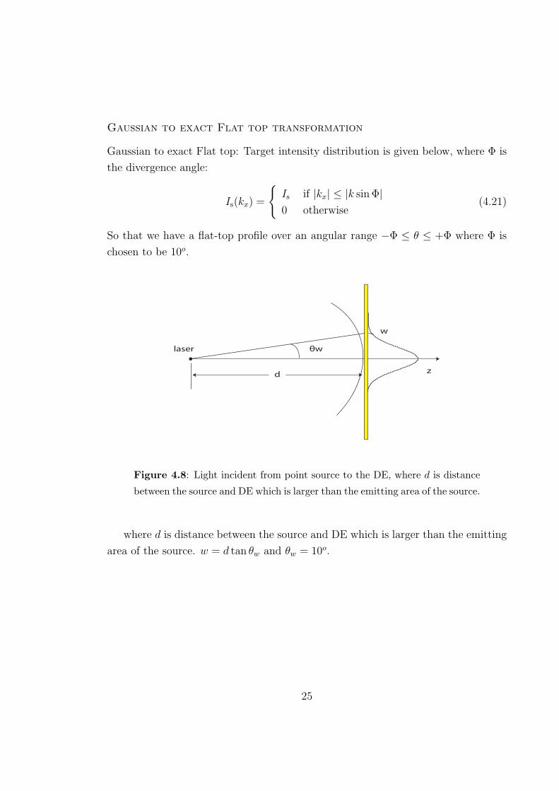
Gaussian to exact Flat top transformation
Gaussian to exact Flat top: Target intensity distribution is given below, where Φ is
the divergence angle:
Is(kx) =
{Is if |kx| ≤ |k sinΦ|0 otherwise
(4.21)
So that we have a flat-top profile over an angular range −Φ ≤ θ ≤ +Φ where Φ is
chosen to be 10o.
θw
w
zd
laser
Figure 4.8: Light incident from point source to the DE, where d is distance
between the source and DE which is larger than the emitting area of the source.
where d is distance between the source and DE which is larger than the emitting
area of the source. w = d tan θw and θw = 10o.
25
dDE
S’
S
dx
dz
θ
θ
θ’
x
k
z
x = d tan θ′
Figure 4.9: Gaussian to flat-top transformation in far zone or kx space.
Here S is point source and S′ is displaced source position and dx is lateral
displacement and dz is longitudinal displacement of the source.
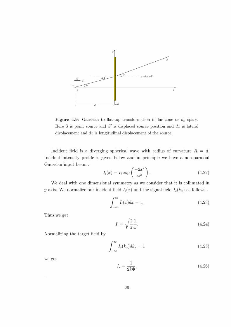
Incident field is a diverging spherical wave with radius of curvature R = d.
Incident intensity profile is given below and in principle we have a non-paraxial
Gaussian input beam :
Ii(x) = Ii exp
(−2x2
ω2
). (4.22)
We deal with one dimensional symmetry as we consider that it is collimated in
y axis. We normalize our incident field Ii(x) and the signal field Is(kx) as follows .∫ ∞
−∞Ii(x)dx = 1. (4.23)
Thus,we get
Ii =
√2
π
1
ω. (4.24)
Normalizing the target field by ∫ ∞
−∞Is(kx)dkx = 1 (4.25)
we get
Is =1
2kΦ. (4.26)
.
26
From map-transform relation we get following relation, i.e., the energy balance
condition is given by ∫ x
0
Ii(x′)dx′ =
∫ kθ′
0
Is(kx′)dkx′ . (4.27)
Integrating this we get
erf
(√2x
ω2
)=
θ′
Φ. (4.28)
Phase function of the element can be found using non paraxial form of grating
equation. We have,
sin θ′ = sin θ +1
k
d
dxΦ(x) (4.29)
and using paraxial form
θ′ = θ +1
k
d
dxΦ(x), (4.30)
where Φ(x) is element phase function, such that θ ≈ tan θ = xdand θ′ ≈ sin θ′ = kx
k.
And we consider unit refractive index on both side of the DE.
kx =k
dx+
d
dxΦ(x), (4.31)
which gives
Φ(x) =
∫ x
0
(kx −
k
dx′)dx′ (4.32)
and thus can be solved analytically. We get
Φ(x) = k
{Φw√2π
[exp
(−2x2
w2
)− 1
]− x2
2d+ Φxerf
(√2x
w
)}. (4.33)
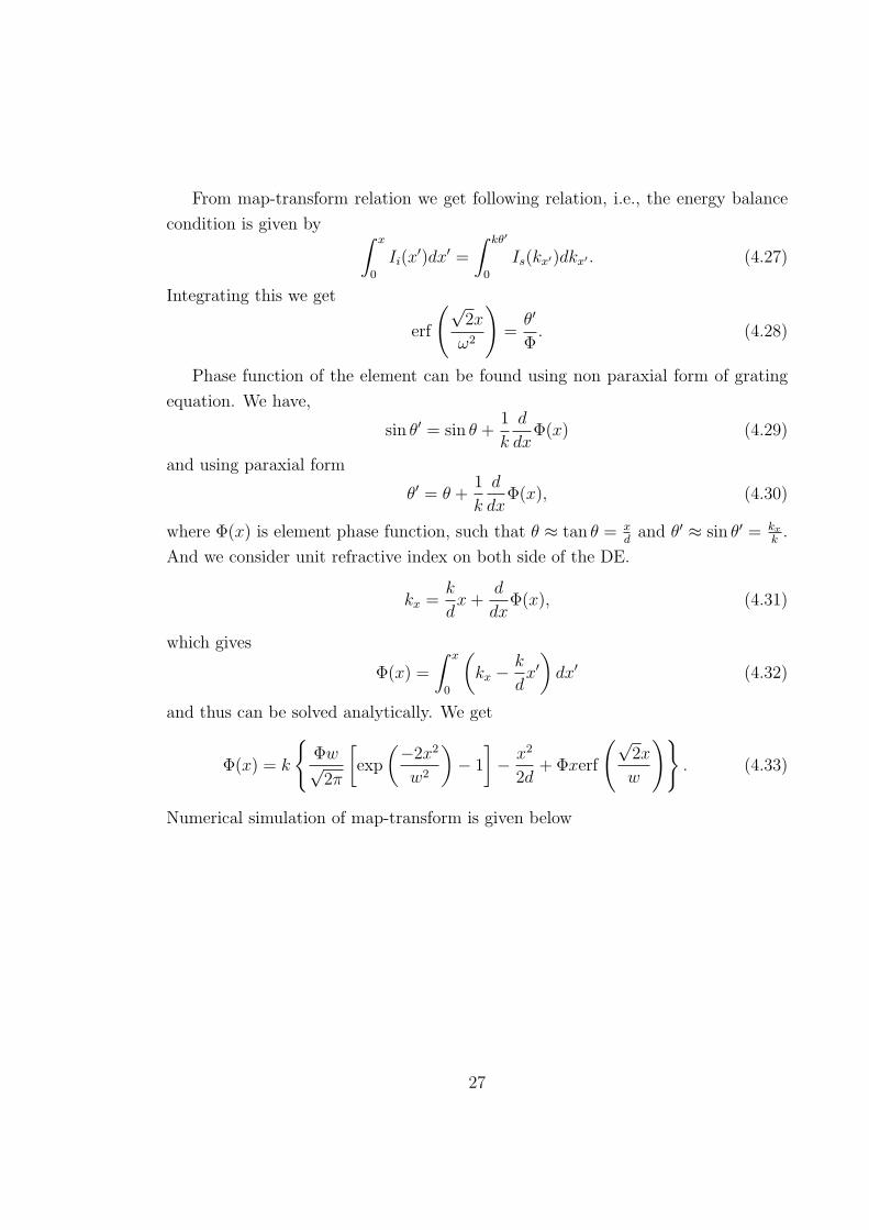
Numerical simulation of map-transform is given below
27
−500 0 500
−3
−2
−1
0
1
2
3
x
φ(x)
(a)
−20 −15 −10 −5 0 5 10 15 200
200
400
600
800
1000
1200
1400
1600
1800
2000
I(K
x)
Angle
(b)
Figure 4.10: (a) Phase function of one dimensional diffractive element gen-
erated from map-transform. (b) Intensity distribution of exact flat top profile
with Φ(x) generated analytically, here blue curve shows the far-field profile
without an element.
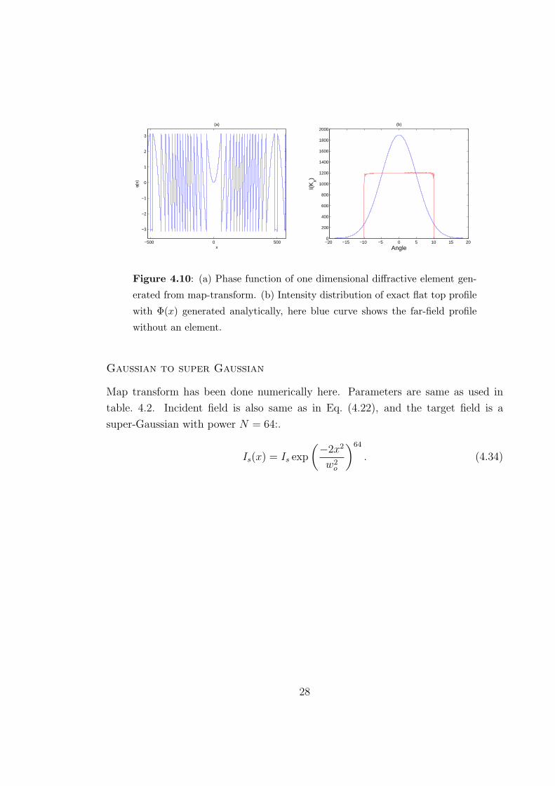
Gaussian to super Gaussian
Map transform has been done numerically here. Parameters are same as used in
table. 4.2. Incident field is also same as in Eq. (4.22), and the target field is a
super-Gaussian with power N = 64:.
Is(x) = Is exp
(−2x2
w2o
)64
. (4.34)
28
−500 0 500
−3
−2
−1
0
1
2
3
x
φ(x)
(a)
−15 −10 −5 0 5 10 15
0
0.5
1
1.5
2
2.5
3
3.5
4
x 107
Angle
I(k x)
(b)
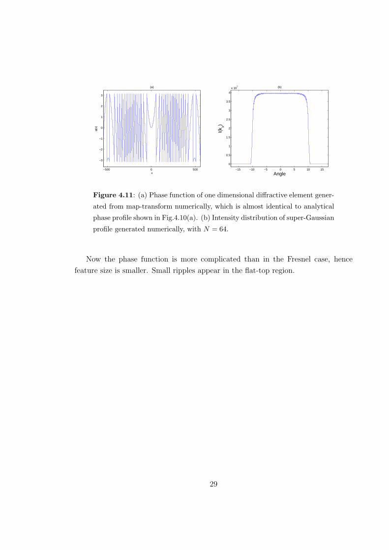
Figure 4.11: (a) Phase function of one dimensional diffractive element gener-
ated from map-transform numerically, which is almost identical to analytical
phase profile shown in Fig.4.10(a). (b) Intensity distribution of super-Gaussian
profile generated numerically, with N = 64.
Now the phase function is more complicated than in the Fresnel case, hence
feature size is smaller. Small ripples appear in the flat-top region.
29
Chapter V
Tolerance analysis
Tolerance analysis is very important as the map transform elements are very sen-
sitive to lateral and longitudinal misalignment. As these elements are designed to
redistribute intensity a small fraction of deviation in source intensity distribution
from designed shape has noticeable effect on obtained target intensity distribution.
The fabricated flat-top elements suffer from sensitivity to fabrication errors such as
profile shape and height errors. The effect of these error is so big that it introduces
the zeroth diffraction order and hence produces an unwanted central intensity peak
and intensity ripple.
5.1 Near-Field: Lateral and longitudinal displacement
We assume that the source is displaced laterally by ∆x and longitudinally by ∆z
from its original position and our incident field has planar phase front. Then the
incident field has the expression
U(x) = exp
[− (x−∆x)2
w2o(1− ∆z
d)2
]. (5.1)
.
30
−800 −600 −400 −200 0 200 400 600 8000
0.2
0.4
0.6
0.8
1
1.2x 10
−3
x
I(x
)
(a)
−800 −600 −400 −200 0 200 400 600 8000
0.2
0.4
0.6
0.8
1
1.2x 10
−3
x
I(x
)
(b)
−800 −600 −400 −200 0 200 400 600 8000
0.2
0.4
0.6
0.8
1
1.2x 10
−3
x
I(x
)
(c)
−800 −600 −400 −200 0 200 400 600 8000
0.2
0.4
0.6
0.8
1
1.2
1.4x 10
−3
x
I(x
)
(d)
−800 −600 −400 −200 0 200 400 600 8000
0.2
0.4
0.6
0.8
1
1.2
1.4x 10
−3
x
I(x
)
(e)
−800 −600 −400 −200 0 200 400 600 8000
1
2
3
4
5
6x 10
4
u
I(u
)
(f)
ω=555
ω=500
ω=600
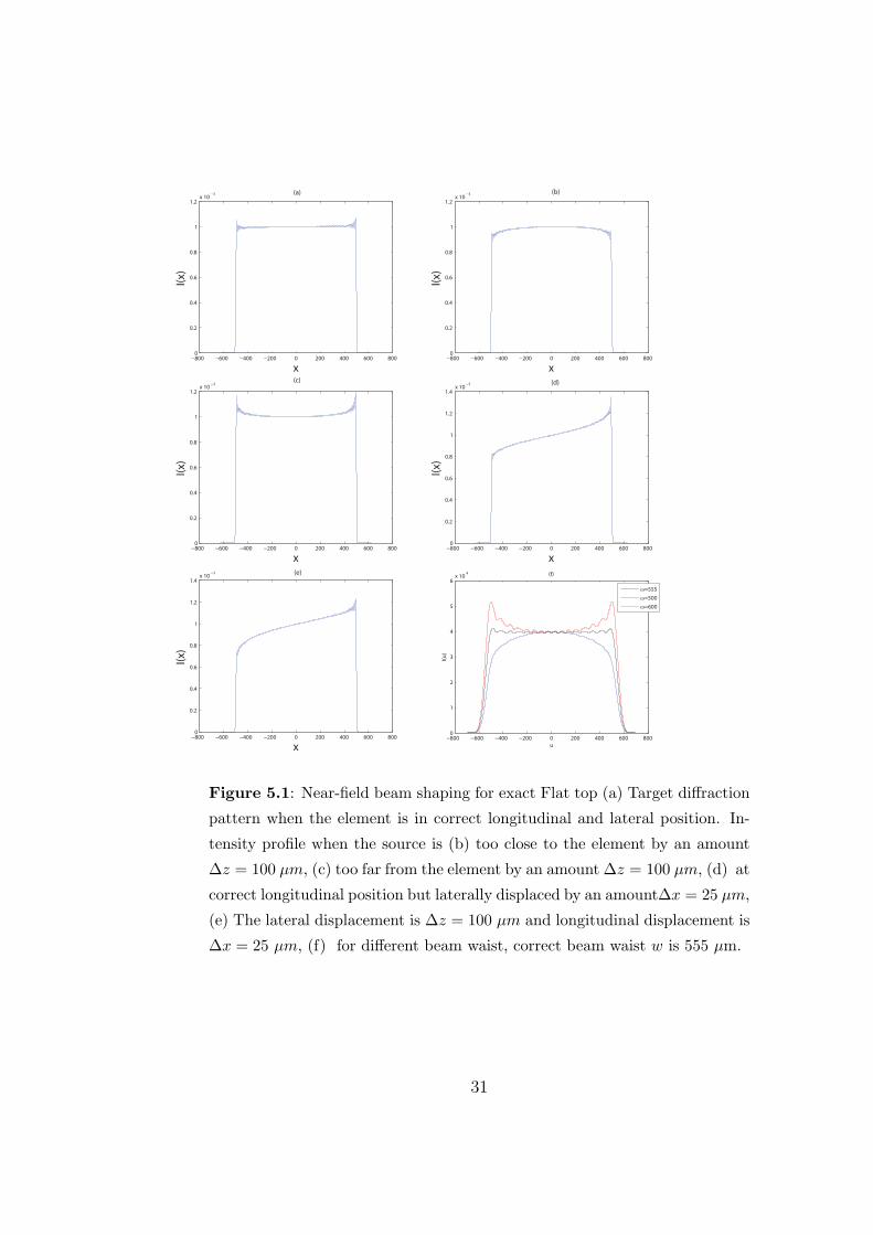
Figure 5.1: Near-field beam shaping for exact Flat top (a) Target diffraction
pattern when the element is in correct longitudinal and lateral position. In-
tensity profile when the source is (b) too close to the element by an amount
∆z = 100 µm, (c) too far from the element by an amount ∆z = 100 µm, (d) at
correct longitudinal position but laterally displaced by an amount∆x = 25 µm,
(e) The lateral displacement is ∆z = 100 µm and longitudinal displacement is
∆x = 25 µm, (f) for different beam waist, correct beam waist w is 555 µm.
31
0 200 400 600 800 1000 1200 1400 16000
0.2
0.4
0.6
0.8
1
1.2
1.4
x
Inte
nsi
ty
Intensity After fresnel propogation
Target Intensity
Incident Intensity
(a)
0 200 400 600 800 1000 1200 1400 16000
0.2
0.4
0.6
0.8
1
1.2
1.4
x
I(x)
Intensity After fresnel propogation
Target Intensity
Incident Intensity
(b)
0 200 400 600 800 1000 1200 1400 16000
0.2
0.4
0.6
0.8
1
1.2
1.4
x
I(x)
Intensity After fresnel propogation
Target Intensity
Incident Intensity
(c)
0 200 400 600 800 1000 1200 1400 16000
0.2
0.4
0.6
0.8
1
1.2
1.4
x
I(x)
Intensity After fresnel propogation
Target Intensity
Incident Intensity
(d)
0 200 400 600 800 1000 1200 1400 16000
0.2
0.4
0.6
0.8
1
1.2
1.4
x
I(x)
Intensity After fresnel propogation
Target Intensity
Incident Intensity
(e)
−800 −600 −400 −200 0 200 400 600 8000
0.5
1
1.5
2
2.5
3
3.5
4
4.5
5x 10
4
u
I(u
)
(f)
ω=555
ω=500
ω=600
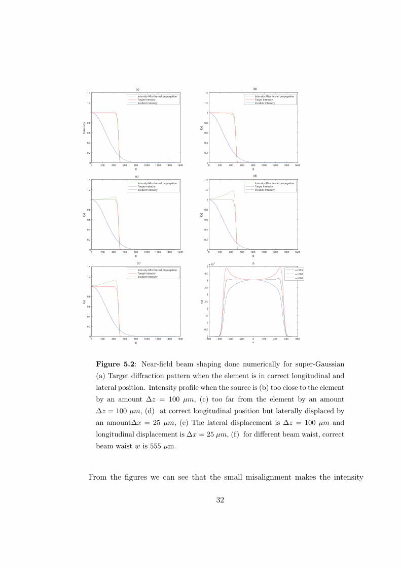
Figure 5.2: Near-field beam shaping done numerically for super-Gaussian
(a) Target diffraction pattern when the element is in correct longitudinal and
lateral position. Intensity profile when the source is (b) too close to the element
by an amount ∆z = 100 µm, (c) too far from the element by an amount
∆z = 100 µm, (d) at correct longitudinal position but laterally displaced by
an amount∆x = 25 µm, (e) The lateral displacement is ∆z = 100 µm and
longitudinal displacement is ∆x = 25 µm, (f) for different beam waist, correct
beam waist w is 555 µm.
From the figures we can see that the small misalignment makes the intensity
32
profile asymmetric. It was seen that positive values ∆z > 0 (distance between S
and DE too large) and an increase in w above its design value both lead to edge
enhancement in the shaped profile. Correspondingly, negative values of ∆z and a
decrease in w gave rise to rounding of the desired flat-top profile. Therefore we
can compensate for variations in w simply by adjusting ∆z slightly in the assembly
phase of the setup in order to get a nice flat-top profile in the Fresnel domain. The
acceptable variation in w is +/−10 µm from the actual w.
5.2 Far-field: Lateral and longitudinal displacement
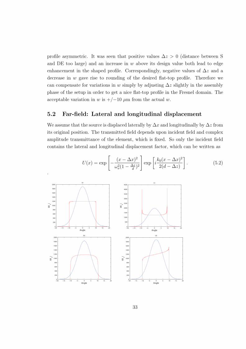
We assume that the source is displaced laterally by ∆x and longitudinally by ∆z from
its original position. The transmitted field depends upon incident field and complex
amplitude transmittance of the element, which is fixed. So only the incident field
contains the lateral and longitudinal displacement factor, which can be written as
U(x) = exp
[− (x−∆x)2
ω2o(1− ∆z
d)2
]exp
[ik0(x−∆x)2
2(d−∆z)
]. (5.2)
.
−20 −15 −10 −5 0 5 10 15 200
200
400
600
800
1000
1200
1400
1600
1800
2000
I(Kx)
Angle
(a)
−20 −15 −10 −5 0 5 10 15 200
200
400
600
800
1000
1200
1400
1600
1800
2000
I(Kx)
Angle
(b)
−20 −15 −10 −5 0 5 10 15 200
500
1000
1500
2000
2500
3000
3500
4000
4500
I(Kx)
Angle
(c)
−20 −15 −10 −5 0 5 10 15 200
200
400
600
800
1000
1200
1400
1600
1800
2000
I(Kx)
Angle
(d)
33
−20 −15 −10 −5 0 5 10 15 200
200
400
600
800
1000
1200
1400
1600
1800
2000
I(Kx)
Angle
(e)
−20 −15 −10 −5 0 5 10 15 200
200
400
600
800
1000
1200
1400
1600
1800
2000
I(Kx)
Angle
(f)
−20 −15 −10 −5 0 5 10 15 200
500
1000
1500
2000
2500
I(Kx)
Angle
(g)
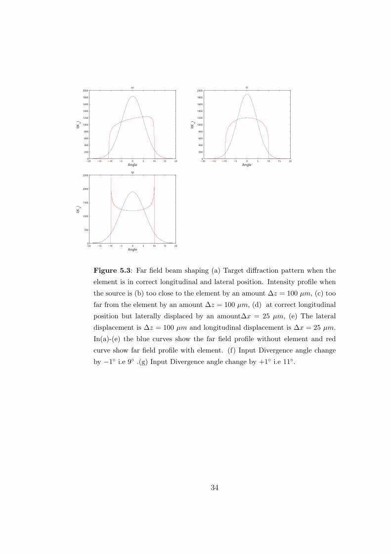
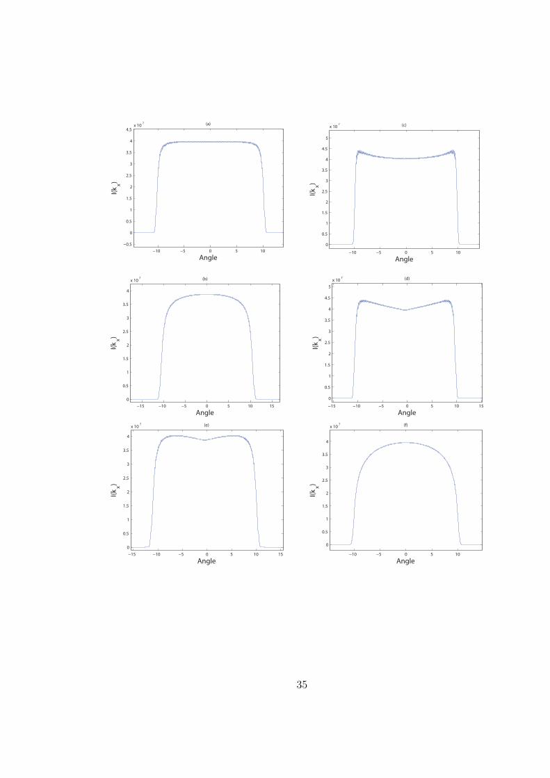
Figure 5.3: Far field beam shaping (a) Target diffraction pattern when the
element is in correct longitudinal and lateral position. Intensity profile when
the source is (b) too close to the element by an amount ∆z = 100 µm, (c) too
far from the element by an amount ∆z = 100 µm, (d) at correct longitudinal
position but laterally displaced by an amount∆x = 25 µm, (e) The lateral
displacement is ∆z = 100 µm and longitudinal displacement is ∆x = 25 µm.
In(a)-(e) the blue curves show the far field profile without element and red
curve show far field profile with element. (f) Input Divergence angle change
by −1◦ i.e 9◦ .(g) Input Divergence angle change by +1◦ i.e 11◦.
34
−10 −5 0 5 10
−0.5
0
0.5
1
1.5
2
2.5
3
3.5
4
4.5x 10
7
Angle
I(k
x)
(a)
−15 −10 −5 0 5 10 15
0
0.5
1
1.5
2
2.5
3
3.5
4
x 107
Angle
I(k
x)
(b)
−10 −5 0 5 10
0
0.5
1
1.5
2
2.5
3
3.5
4
4.5
5
x 107
Angle
I(k
x)
(c)
−15 −10 −5 0 5 10 15
0
0.5
1
1.5
2
2.5
3
3.5
4
4.5
5
x 107
Angle
I(k
x)
(d)
−15 −10 −5 0 5 10 15
0
0.5
1
1.5
2
2.5
3
3.5
4
x 107
Angle
I(k
x)
(e)
−10 −5 0 5 10
0
0.5
1
1.5
2
2.5
3
3.5
4
x 107
Angle
I(k
x)
(f)
35
−10 −5 0 5 10
0
0.5
1
1.5
2
2.5
3
3.5
4
4.5
5
x 107
Angle
I(k
x)
(g)
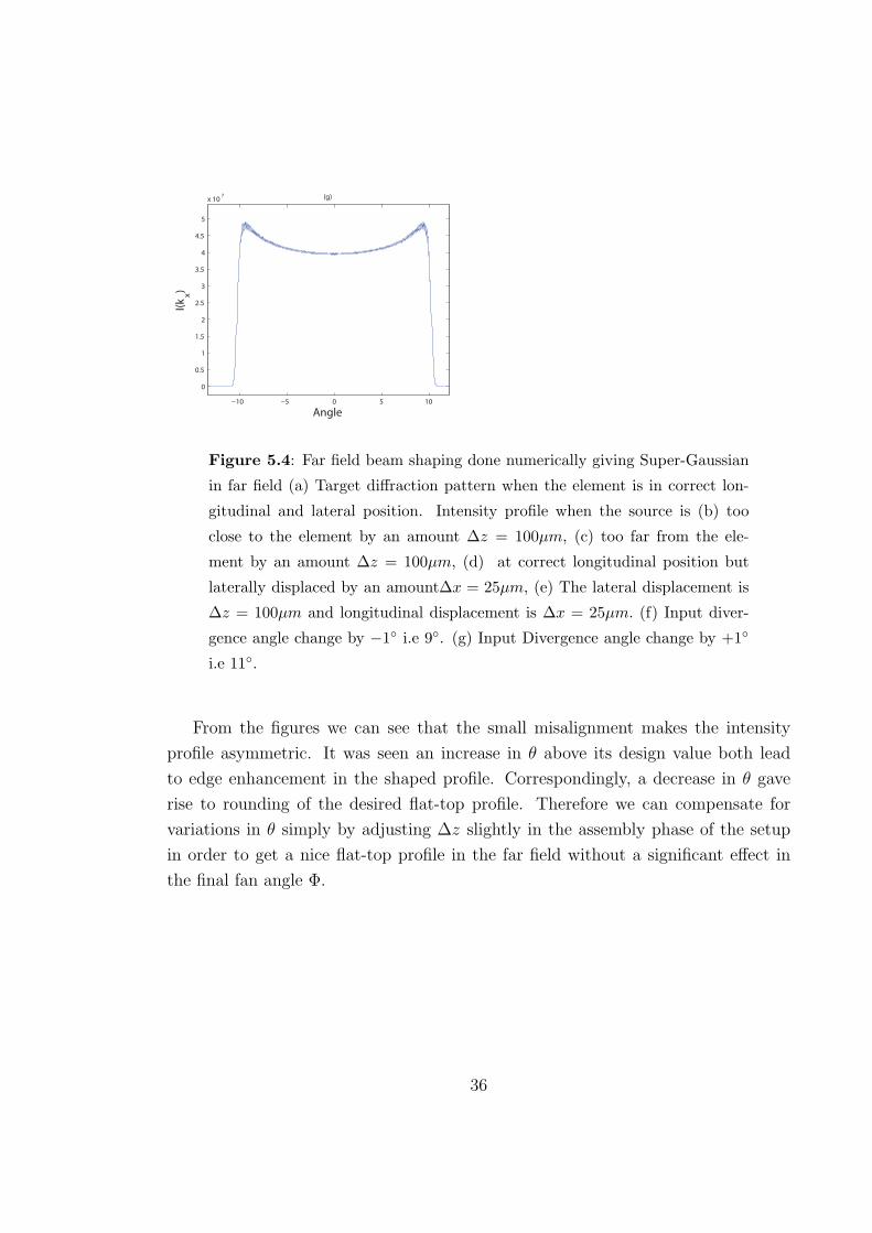
Figure 5.4: Far field beam shaping done numerically giving Super-Gaussian
in far field (a) Target diffraction pattern when the element is in correct lon-
gitudinal and lateral position. Intensity profile when the source is (b) too
close to the element by an amount ∆z = 100µm, (c) too far from the ele-
ment by an amount ∆z = 100µm, (d) at correct longitudinal position but
laterally displaced by an amount∆x = 25µm, (e) The lateral displacement is
∆z = 100µm and longitudinal displacement is ∆x = 25µm. (f) Input diver-
gence angle change by −1◦ i.e 9◦. (g) Input Divergence angle change by +1◦
i.e 11◦.
From the figures we can see that the small misalignment makes the intensity
profile asymmetric. It was seen an increase in θ above its design value both lead
to edge enhancement in the shaped profile. Correspondingly, a decrease in θ gave
rise to rounding of the desired flat-top profile. Therefore we can compensate for
variations in θ simply by adjusting ∆z slightly in the assembly phase of the setup
in order to get a nice flat-top profile in the far field without a significant effect in
the final fan angle Φ.
36

Chapter VI
Characterization and fabrication errors
The key to a successful design is correct simulation, realization of simulated function
by fabrication, characterization of the element to check if the element gives the
desired output and the final step is the possibility of redesign if the desired output
is not obtained. All the steps are discussed in detail in this chapter.
6.1 Simulation
All the designs were simulated in MATLAB and was discussed in chapter IV and
there tolerances in chapter V. In order to verify that the codes were generated
properly, analytical map transform phase functions were simulated numerically and
analytically. And they were matched. For example in Fig. 6.1 Gaussian to Gaussian
transformation is done using map transform method analytically and numerically.
37
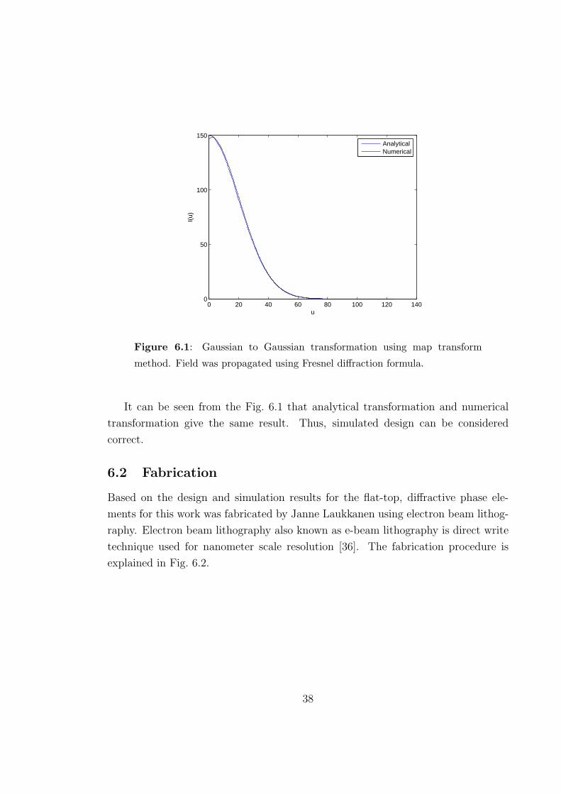
0 20 40 60 80 100 120 1400
50
100
150
u
I(u)
AnalyticalNumerical
Figure 6.1: Gaussian to Gaussian transformation using map transform
method. Field was propagated using Fresnel diffraction formula.
It can be seen from the Fig. 6.1 that analytical transformation and numerical
transformation give the same result. Thus, simulated design can be considered
correct.
6.2 Fabrication
Based on the design and simulation results for the flat-top, diffractive phase ele-
ments for this work was fabricated by Janne Laukkanen using electron beam lithog-
raphy. Electron beam lithography also known as e-beam lithography is direct write
technique used for nanometer scale resolution [36]. The fabrication procedure is
explained in Fig. 6.2.
38
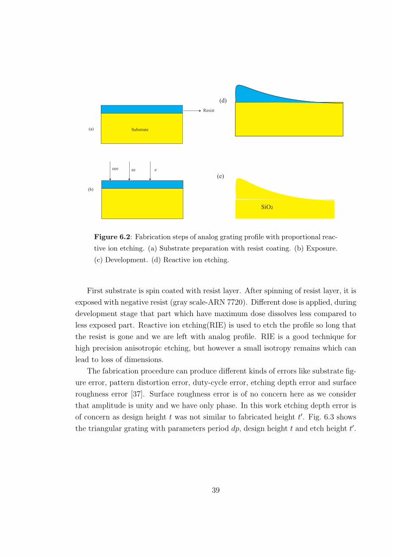
Substrate
Resist
(a)
(b)
eee ee e
(d)
(e)
SiO2
Figure 6.2: Fabrication steps of analog grating profile with proportional reac-
tive ion etching. (a) Substrate preparation with resist coating. (b) Exposure.
(c) Development. (d) Reactive ion etching.
First substrate is spin coated with resist layer. After spinning of resist layer, it is
exposed with negative resist (gray scale-ARN 7720). Different dose is applied, during
development stage that part which have maximum dose dissolves less compared to
less exposed part. Reactive ion etching(RIE) is used to etch the profile so long that
the resist is gone and we are left with analog profile. RIE is a good technique for
high precision anisotropic etching, but however a small isotropy remains which can
lead to loss of dimensions.
The fabrication procedure can produce different kinds of errors like substrate fig-
ure error, pattern distortion error, duty-cycle error, etching depth error and surface
roughness error [37]. Surface roughness error is of no concern here as we consider
that amplitude is unity and we have only phase. In this work etching depth error is
of concern as design height t was not similar to fabricated height t′. Fig. 6.3 shows
the triangular grating with parameters period dp, design height t and etch height t′.
39
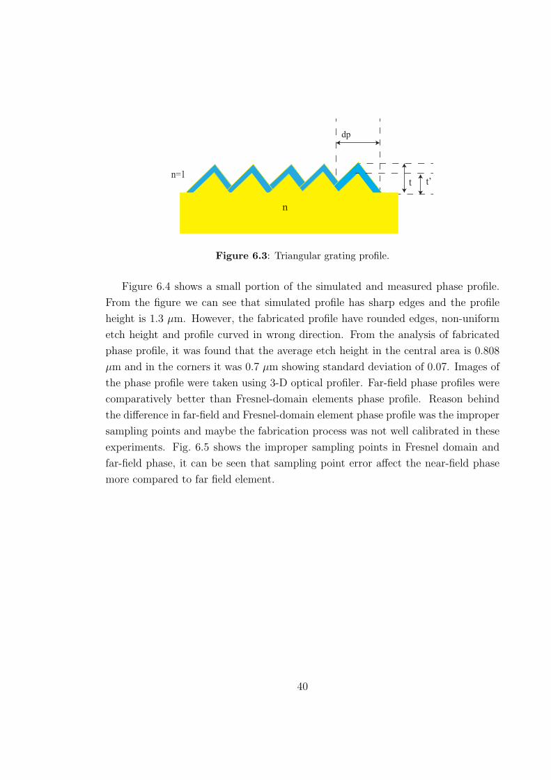
t
dp
n=1t’
n
Figure 6.3: Triangular grating profile.
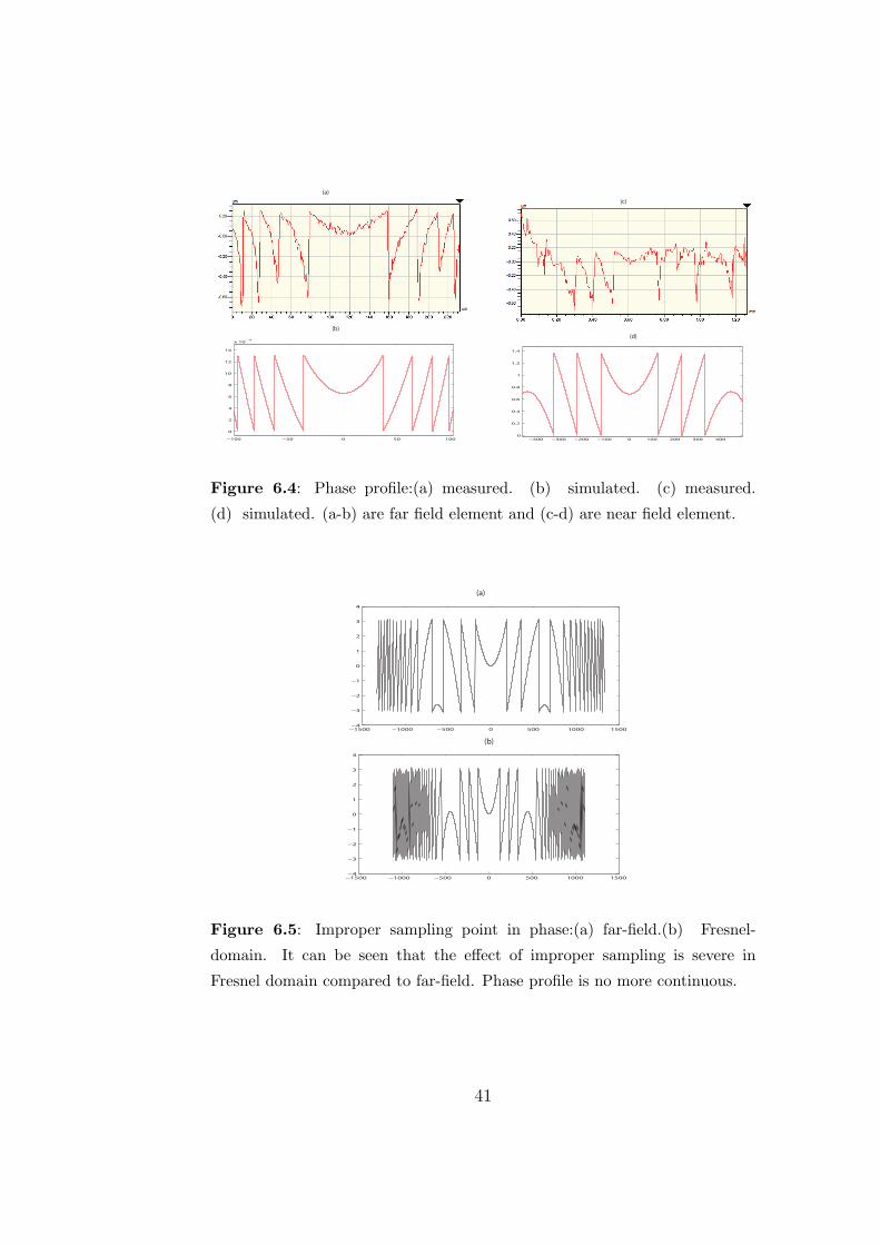
Figure 6.4 shows a small portion of the simulated and measured phase profile.
From the figure we can see that simulated profile has sharp edges and the profile
height is 1.3 µm. However, the fabricated profile have rounded edges, non-uniform
etch height and profile curved in wrong direction. From the analysis of fabricated
phase profile, it was found that the average etch height in the central area is 0.808
µm and in the corners it was 0.7 µm showing standard deviation of 0.07. Images of
the phase profile were taken using 3-D optical profiler. Far-field phase profiles were
comparatively better than Fresnel-domain elements phase profile. Reason behind
the difference in far-field and Fresnel-domain element phase profile was the improper
sampling points and maybe the fabrication process was not well calibrated in these
experiments. Fig. 6.5 shows the improper sampling points in Fresnel domain and
far-field phase, it can be seen that sampling point error affect the near-field phase
more compared to far field element.
40
(a)
(b)
−100 −50 0 50 100
0
2
4
6
8
10
12
14
x 10−4
−400 −300 −200 −100 0 100 200 300 400
0
0.2
0.4
0.6
0.8
1
1.2
1.4
(c)
(d)
Figure 6.4: Phase profile:(a) measured. (b) simulated. (c) measured.
(d) simulated. (a-b) are far field element and (c-d) are near field element.
−1500 −1000 −500 0 500 1000 1500−4
−3
−2
−1
0
1
2
3
4
−1500 −1000 −500 0 500 1000 1500−4
−3
−2
−1
0
1
2
3
4
(a)
(b)
Figure 6.5: Improper sampling point in phase:(a) far-field.(b) Fresnel-
domain. It can be seen that the effect of improper sampling is severe in
Fresnel domain compared to far-field. Phase profile is no more continuous.
41
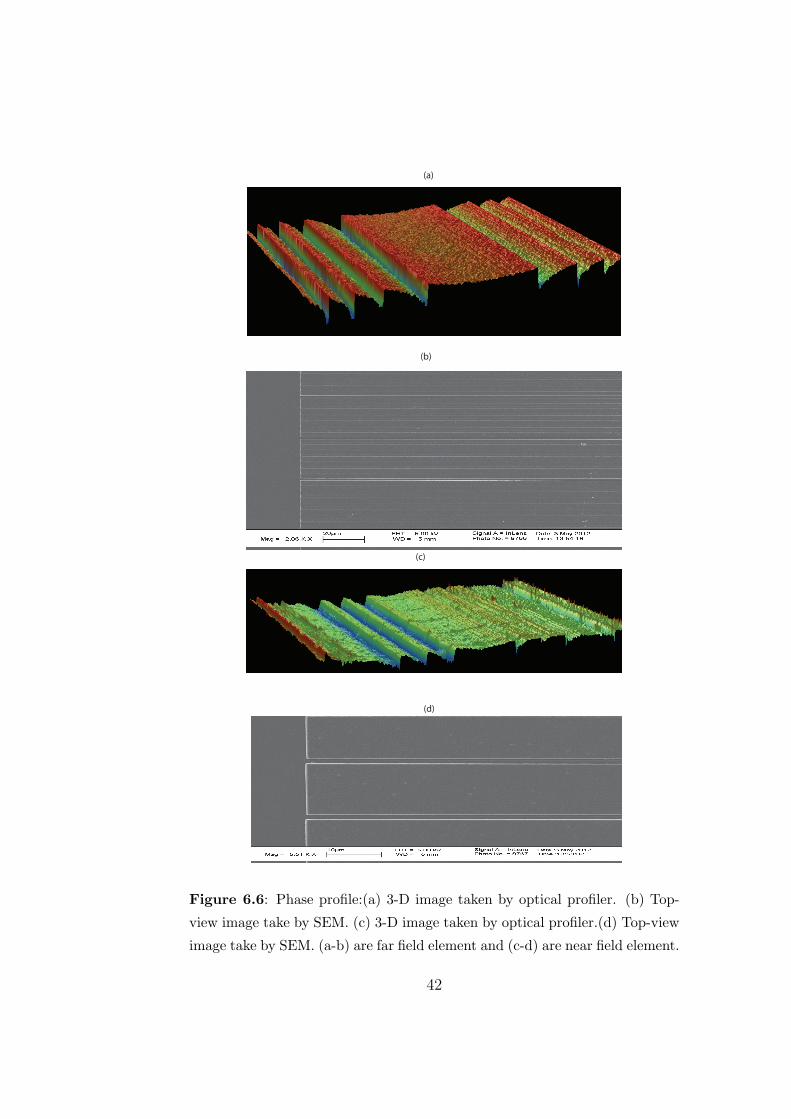
(a)
(b)
(c)
(d)
Figure 6.6: Phase profile:(a) 3-D image taken by optical profiler. (b) Top-
view image take by SEM. (c) 3-D image taken by optical profiler.(d) Top-view
image take by SEM. (a-b) are far field element and (c-d) are near field element.
42
6.2.1 Effect of etch depth error
Let us assume that we have an ideal phase function Φ(x). And this element has
maximum height of the surface relief structure as t′ instead of the design value t
because of error in etch depth. Then we can define our transmission function as
tx(x) = exp[iαΦ(x)] (6.1)
where α is the ratio of fabricated height t′ and designed height t and it doesn’t change
the periodicity of ideal phase function. Transmittance function can be elaborated
by a generalized Fourier series expansion as [?]alpha)
tx(x) =∞∑
m=−∞
Gm exp[imΦ(x)], (6.2)
where m is the diffraction order and coefficient Gm is
Gm =1
2π
∫ 2π
0
exp[i(α−m)Φ(x)]dΦ(x). (6.3)
which gives
Gm = sinc(α−m) exp[iπ(α−m)]. (6.4)
If α = 1, then we can say that the wave is generated perfectly as generalized Fourier
series contains only the first order term m = 1. But if α = 1 then, there would
be more of interference caused by generated noise fields and it would lead to loss of
signal quality, and reduced diffraction efficiency.
There is another method for fabrication etch depth error analysis. The direct
scaling technique can be described elegantly and generally as follows. If the ideal
phase function of the DE is ϕ(x), we can generate its modulo 2π quantized version
in the interval [−π, π] using
ϕmod(x) = arg {exp [iϕ(x)]} . (6.5)
In case of scaling error described by a factor α, the phase function scaled to an
internal [−απ, απ] is αϕmod(x) and the transmission function of the element is
t(x) = exp [iαϕmod(x)] . (6.6)
This transmission function can be multiplied by the incident field the result can
be used directly to propagate the output field into the target plane. The result is
43
then same as that given by the generalized order method when the number of orders
included in the analysis is sufficiently large.
In order to explain it more explicitly, would apply the above mentioned analysis
to triangular grating first as phase function of the elements designed in this thesis
are similar to triangular grating and then to actual phase functions of the elements
designed for this thesis. Phase function triangular grating is given in Eq.(6.7).
Vm(x, y) = exp[−i2πmx/d] (6.7)
The generalized orders are obtained by inserting the phase function into
V (x, y) =∞∑
m=−∞
GmVm(x, y). (6.8)
Here V (x, y) is the field immediately after the element. Thus, different terms in
Eq. (6.8) represent so-called generalized diffraction orders of the element, which
have diffraction efficiencies as
ηm = ηm = |Gm|2 . (6.9)
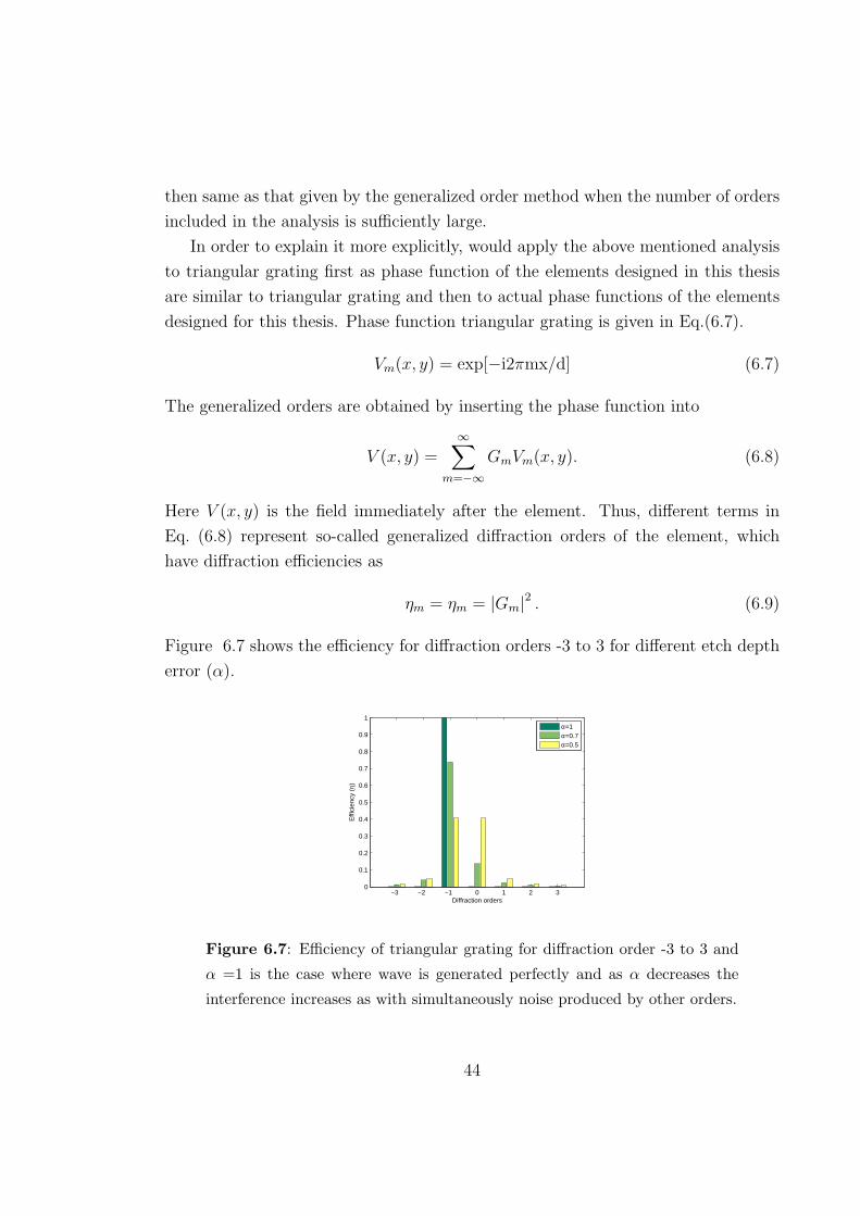
Figure 6.7 shows the efficiency for diffraction orders -3 to 3 for different etch depth
error (α).
−3 −2 −1 0 1 2 30
0.1
0.2
0.3
0.4
0.5
0.6
0.7
0.8
0.9
1
Diffraction orders
Effi
cien
cy (
η)
α=1α=0.7α=0.5
Figure 6.7: Efficiency of triangular grating for diffraction order -3 to 3 and
α =1 is the case where wave is generated perfectly and as α decreases the
interference increases as with simultaneously noise produced by other orders.
44
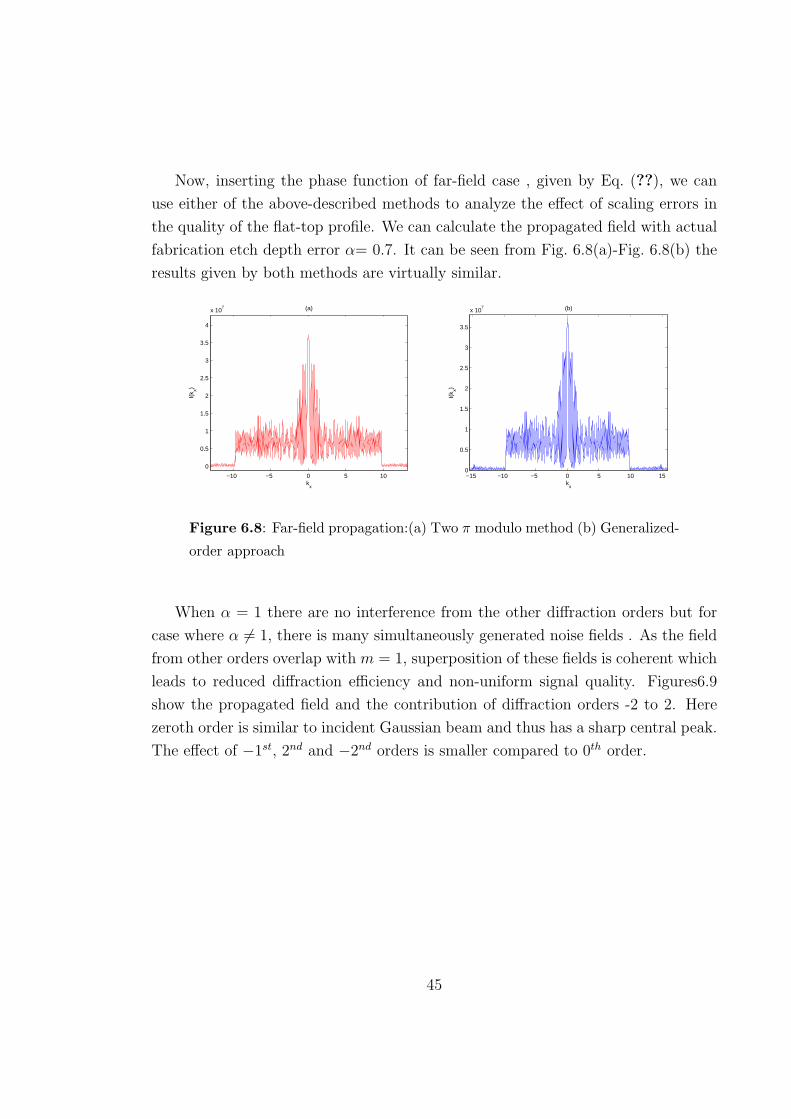
Now, inserting the phase function of far-field case , given by Eq. (??), we can
use either of the above-described methods to analyze the effect of scaling errors in
the quality of the flat-top profile. We can calculate the propagated field with actual
fabrication etch depth error α= 0.7. It can be seen from Fig. 6.8(a)-Fig. 6.8(b) the
results given by both methods are virtually similar.
−10 −5 0 5 10
0
0.5
1
1.5
2
2.5
3
3.5
4
x 107
kx
I(k x)
(a)
−15 −10 −5 0 5 10 150
0.5
1
1.5
2
2.5
3
3.5
x 107 (b)
kx
I(k x)
Figure 6.8: Far-field propagation:(a) Two π modulo method (b) Generalized-
order approach
When α = 1 there are no interference from the other diffraction orders but for
case where α = 1, there is many simultaneously generated noise fields . As the field
from other orders overlap with m = 1, superposition of these fields is coherent which
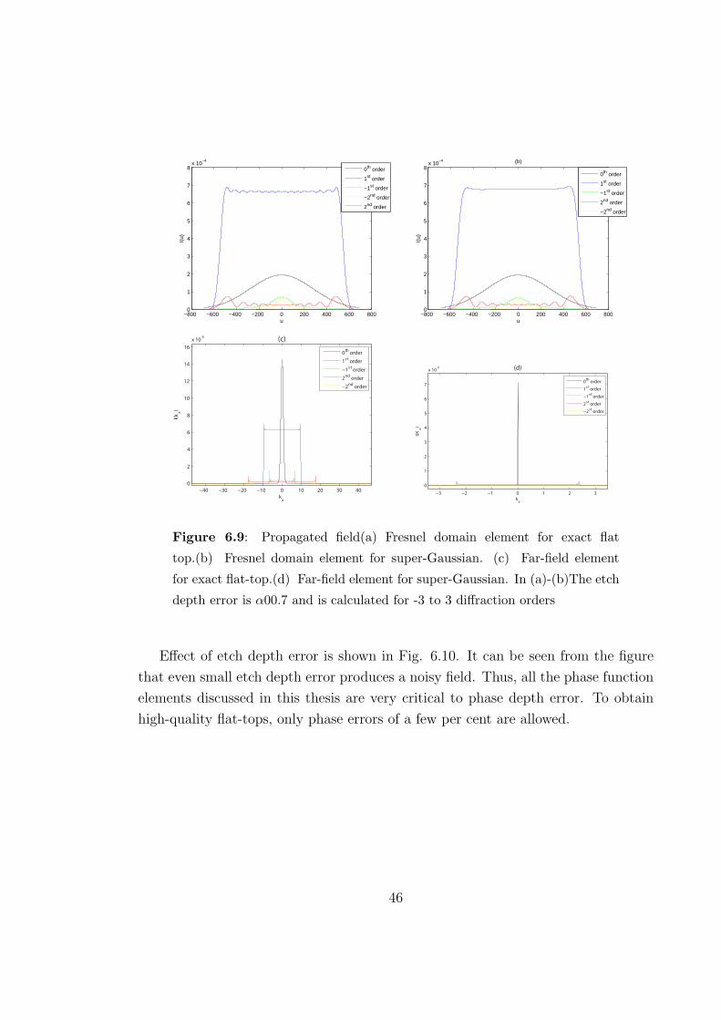
leads to reduced diffraction efficiency and non-uniform signal quality. Figures6.9
show the propagated field and the contribution of diffraction orders -2 to 2. Here
zeroth order is similar to incident Gaussian beam and thus has a sharp central peak.
The effect of −1st, 2nd and −2nd orders is smaller compared to 0th order.
45
−800 −600 −400 −200 0 200 400 600 8000
1
2
3
4
5
6
7
8x 10
−4
u
I(u)
0th order
1st order
−1st order
−2nd order
2nd order
−800 −600 −400 −200 0 200 400 600 8000
1
2
3
4
5
6
7
8x 10
−4
u
I(u)
(b)
0th order
1st order
−1st order
2nd order
−2nd order
−40 −30 −20 −10 0 10 20 30 40
0
2
4
6
8
10
12
14
16
x 106
kx
I(k
x)
(a)
0th
order
1st
order
−1st
order
2nd
order
−2nd
order
(c)
−3 −2 −1 0 1 2 3
0
1
2
3
4
5
6
7
x 109
kx
I(K
x)
(a)
0th
order
1st
order
−1st
order
2st
order
−2st
order
(d)
Figure 6.9: Propagated field(a) Fresnel domain element for exact flat
top.(b) Fresnel domain element for super-Gaussian. (c) Far-field element
for exact flat-top.(d) Far-field element for super-Gaussian. In (a)-(b)The etch
depth error is α00.7 and is calculated for -3 to 3 diffraction orders
Effect of etch depth error is shown in Fig. 6.10. It can be seen from the figure
that even small etch depth error produces a noisy field. Thus, all the phase function
elements discussed in this thesis are very critical to phase depth error. To obtain
high-quality flat-tops, only phase errors of a few per cent are allowed.
46
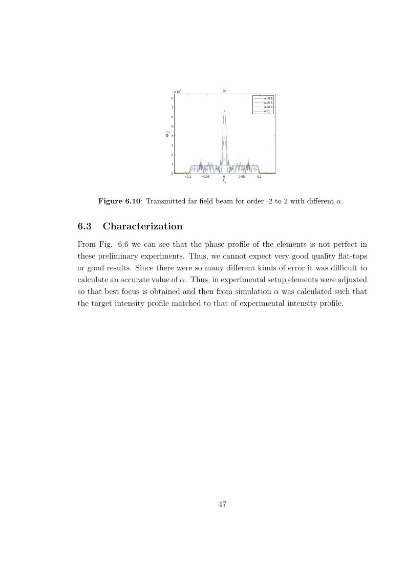
−0.1 −0.05 0 0.05 0.10
1
2
3
4
5
6
7
8
x 108
kx
I(k x)
(b)
α=0.5α=0.8α=0.9α=1
Figure 6.10: Transmitted far field beam for order -2 to 2 with different α.
6.3 Characterization
From Fig. 6.6 we can see that the phase profile of the elements is not perfect in
these preliminary experiments. Thus, we cannot expect very good quality flat-tops
or good results. Since there were so many different kinds of error it was difficult to
calculate an accurate value of α. Thus, in experimental setup elements were adjusted
so that best focus is obtained and then from simulation α was calculated such that
the target intensity profile matched to that of experimental intensity profile.
47
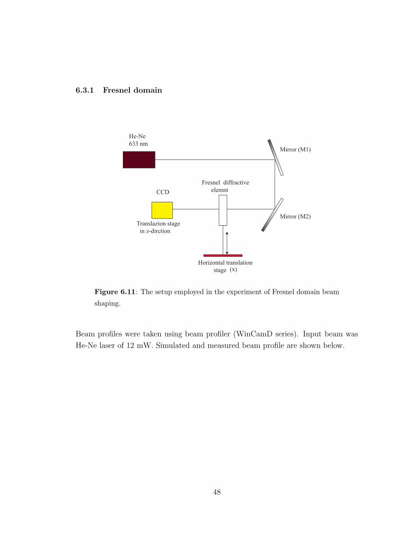
6.3.1 Fresnel domain
He-Ne
633 nmMirror (M1)
Mirror (M2)
CCD
Fresnel diffractive
elemnt
Horizontal translation
stage (x)
Translazion stage
in z-dirction
Figure 6.11: The setup employed in the experiment of Fresnel domain beam
shaping.
Beam profiles were taken using beam profiler (WinCamD series). Input beam was
He-Ne laser of 12 mW. Simulated and measured beam profile are shown below.
48

Fresnel domain:exact flat-top
(a)
−20 −15 −10 −5 0 5 10 15 200
0.5
1
1.5
2
2.5
3
x 105
u
I(u
)
(c)(b)
Figure 6.12: Target intensity profile (a) measured using beam profiler. Hor-
izontal axis shows flat-top direction and vertical axis shows Gaussian beam
direction. (b) simulated intensity profile with α=0.7.
From the figure we can see that the simulated result and the measured result are
approximately similar. We could assume that if our element was perfect or had
smaller error then it would have worked perfectly.
49
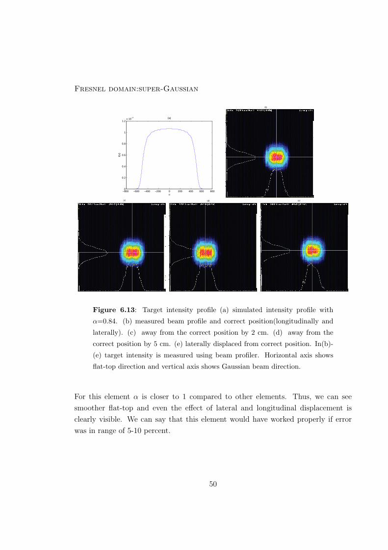
Fresnel domain:super-Gaussian
−800 −600 −400 −200 0 200 400 600 8000
0.2
0.4
0.6
0.8
1
1.2x 10
−3 (a)
u
I(u)
(b)
(c) (d) (e)
Figure 6.13: Target intensity profile (a) simulated intensity profile with
α=0.84. (b) measured beam profile and correct position(longitudinally and
laterally). (c) away from the correct position by 2 cm. (d) away from the
correct position by 5 cm. (e) laterally displaced from correct position. In(b)-
(e) target intensity is measured using beam profiler. Horizontal axis shows
flat-top direction and vertical axis shows Gaussian beam direction.
For this element α is closer to 1 compared to other elements. Thus, we can see
smoother flat-top and even the effect of lateral and longitudinal displacement is
clearly visible. We can say that this element would have worked properly if error
was in range of 5-10 percent.
50
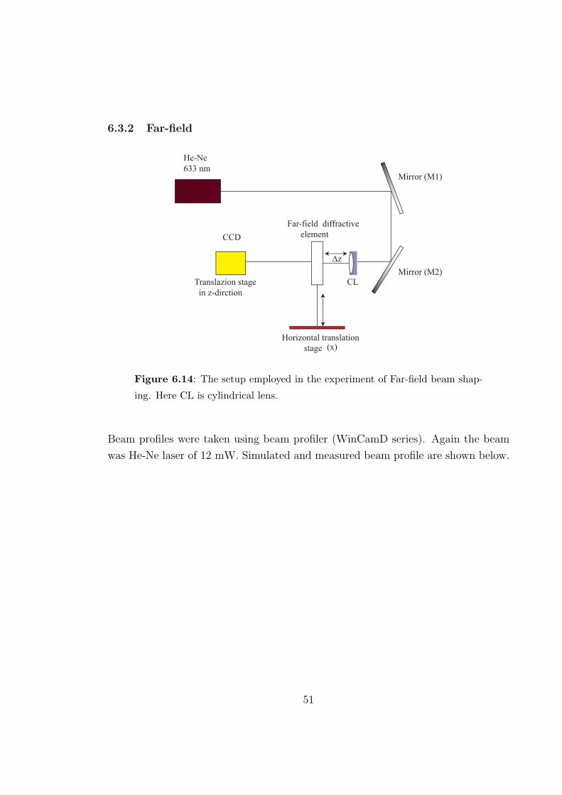
6.3.2 Far-field
He-Ne
633 nmMirror (M1)
Mirror (M2)
CCD
Far-field diffractive
element
Horizontal translation
stage (x)
Translazion stage
in z-dirction
CL
∆z
Figure 6.14: The setup employed in the experiment of Far-field beam shap-
ing. Here CL is cylindrical lens.
Beam profiles were taken using beam profiler (WinCamD series). Again the beam
was He-Ne laser of 12 mW. Simulated and measured beam profile are shown below.
51
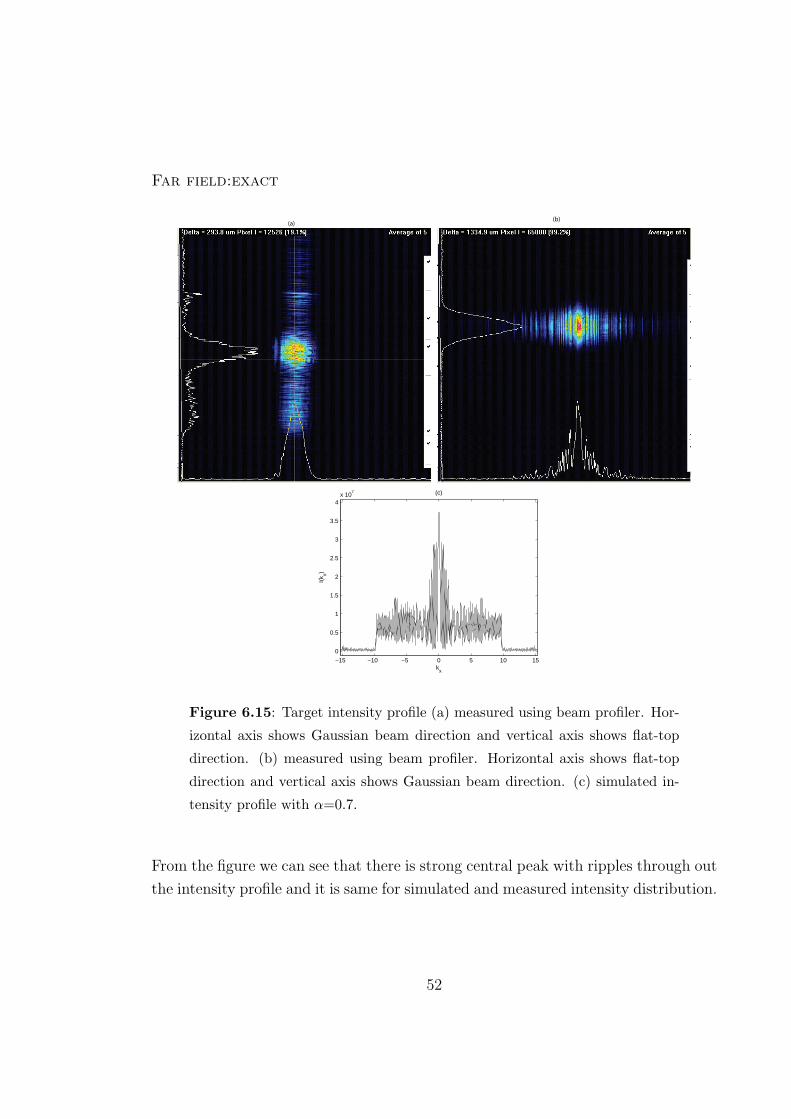
Far field:exact
(a)(b)
−15 −10 −5 0 5 10 15
0
0.5
1
1.5
2
2.5
3
3.5
4x 10
7
kx
I(k x)
(c)
Figure 6.15: Target intensity profile (a) measured using beam profiler. Hor-
izontal axis shows Gaussian beam direction and vertical axis shows flat-top
direction. (b) measured using beam profiler. Horizontal axis shows flat-top
direction and vertical axis shows Gaussian beam direction. (c) simulated in-
tensity profile with α=0.7.
From the figure we can see that there is strong central peak with ripples through out
the intensity profile and it is same for simulated and measured intensity distribution.
52
Far field:super-Gaussian
(a)
−1 −0.5 0 0.5 1
0
1
2
3
4
5
6
7
8
x 108
kx
I(k
x)
(b))
Figure 6.16: Target intensity profile (a) measured using beam profiler. Hor-
izontal axis shows flat-top direction and vertical axis shows Gaussian beam
direction. (b) simulated intensity profile with α=0.7.
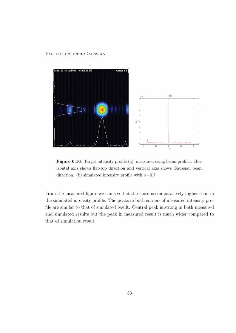
From the measured figure we can see that the noise is comparatively higher than in
the simulated intensity profile. The peaks in both corners of measured intensity pro-
file are similar to that of simulated result. Central peak is strong in both measured
and simulated results but the peak in measured result is much wider compared to
that of simulation result.
53
Chapter VII
Conclusion
The diffractive beam shaping element is thin single element which can be installed
easily in any optical setup. The beam shaping elements in this thesis are designed
for Fresnel domain and far-field. Simulated results show that it possible to generate
smooth flat-top with high efficiency and uniform intensity. Fresnel domain elements
are critical about beam diameter, sometimes measured beam waist by CCD camera
is not actual or real beam diameter as sometimes CCD camera are nonlinear. Then,
we can let the laser beam propagate until the distance where the laser waist becomes
accurate to design beam waist. For far-field case divergence angle is a critical issue
we can compensate for variations in the divergence of the laser beam simply by
adjusting the distance between the source and the element.
For both Fresnel and far-field case it was seen that positioning of the element was
critical theoretically and experimentally. Transverse positioning errors were found to
give non-symmetric profiles, it appeared that errors of beam waist w, longitudinal
displacement(∆z), and divergence angle (Φ) lead to qualitatively similar effects:
positive values ∆z > 0 (distance between S and DE too large), an increase of Φ and
w above there design values both lead to edge enhancement in the shaped profile.
Correspondingly, negative values of ∆z, as well as decrease in Φ and w give rise to
rounding of the desired flat-top profile. Therefore we can compensate for variations
in Φ and w simply by adjusting ∆z slightly in the assembly phase of the setup
in order to get a nice flat-top profile and use of high-order super-Gaussian target
profiles.
The beam shaping element of present type had minimum local periods of ∼ 5λ,
and it was very difficult to fabricate highly efficient DEs. Thus, they suffered from
54
etch depth errors of 30 percent, which led to scattering of light into higher generalized
orders of the DE. It was seen theoretically from simulated results and experimentally
that the DE is very critical to profile height. As a result a wrong profile height led
to generalized order producing high interference and reduced efficiency, thus leading
asymmetry in the output profile. Use of diode pumped laser of wavelength ∼ 457
nm resulted in reduction of etch depth error by 5 percent. From simulated results
it was found that the allowed error range was 2 percent but still this range can vary
depending on application. Thus all output profiles showed a sharp central peak and
it reduced with reduction in error.
At the time of writing this thesis, only few critical parameters were considered
but many improvements and analysis are possible in future, as will be explained in
chapter VIII.
55
Chapter VIII
Future-work
Beam shaping elements of present type have triangular local profile which have
etch depth error and the triangular edges are rounded, which leads to scattering of
light into higher generalized orders of the DE. Thus, in future more trial rounds in
fabrication should be done to get the error in profile height small enough. Grating
profiles with step or staircase form should be designed to reduce fabrication errors.
Carrier grating in x direction should be used for designs with small divergence angle
and carrier grating in y direction should be used for large angles to separate different
diffraction orders, which will help in reducing interference caused by generalized
orders and thus improving flat-top quality of our design.
Complex amplitude transmission approach was used to calculate the efficiency of
different orders but in future rigorous diffraction theory like Fourier modal method
(FMM) should be used in the analysis and design. FMM is a good approach for non
paraxial cases like our case of focusing a laser beam on the grating with a cylindrical
lens as it helps us to get refined structural parameters and accurate efficiency. One
future goal is to design DE element for flat-top profile with supercontinum beams
as the most of the spectral components experience a totally wrong phase delay like
our present elements.
56
Bibliography
[1] F.M. Dickey and S.C. Holswade, Laser Beam Shaping: Theory and Techniques,
Mercel Dekker, (2000).
[2] J. Turunen and F.Wyrowski, ed. , Diffractive Optics for Industrial and Com-
mercial Applications, Akademie Verlag, Berlin, Germany, pp. 426 (1997).
[3] H. P. Herzig, ed., Micro-Optics: Elements, Systems And Applications, Taylor
and Francis, London, 1997.
[4] W. Daschner, P. Long, R. Stein, C. Wu, and S. Lee, One step lithography
for mass production of multilevel diffractive optical elements using high-energy
beam sensitive (HEBS) grey-level mask, Proc. SPIE, 2689, pp. 153-155 (1996).
[5] C. Hong-Wen, H. Ching-Ju, and L. Chung-Chi, Development of a novel optical
CT employing a laser to create a collimated line-source with a flat-top intensity
distribution, Radiation Measurements, 46, pp. 1932-1935 (2011).
[6] M. F. Chen, K. M. Lin, and Y. S. Ho, Laser annealing process of ITO thin
films using beam shaping technology, Optics and Lasers in Engineering, 50,
pp. 491-495 (2012).
[7] G. Raciukaitis, E. Stankevicius, P. Gecys, M. Gedvilas, C. Bischoff, E. Jaeger,
U. Umhofer and F. Volklein, Laser processing by using diffractive optical laser
beam shaping technique, Journal of Laser Micro/Nanoengineering, 6, pp. 37-43
(2011).
57
[8] O. Homburg, D. Hauschild, F. Kubacki, and V. Lissotschenko, Efficient beam
shaping for high-power laser applications. Proc. SPIE, 6216, pp. 621-608
(2006).
[9] E. B. Kley, M. Cumme, L. C. Wittig, M. Thieme and W. Gabler, Beam shaping
elements for holographic application, Proc. SPIE, 4179, pp. 58 - 64 (2000).
[10] O. Bryndahl, Optical map transformation, Opt. Commun., 10, pp. 164-169
(1974).
[11] O. Bryndahl, Geometrical map transforms in optics, J. Opt. Soc. Am. 64, pp.
1092-1099 (1974).
[12] C. N. Kurtz, H. O. Hoadley, and J. J. DePalma, Design and synthesis of random
phase diffusers, J.Opt.Soc.Am., 68, pp. 1080-1092 (1973).
[13] B. Mercier, J.P. Rousseau, A. Jullien, and L. Antonucci, Nonlinear beam shaper
for femtosecond laser pulses, from Gaussian to flat-top profile, Opt. Commun.,
283, pp. 2900-2907 (2010).
[14] K. Sehun and O. Kyunghwan, 1D Bessel-like beam generation by highly direc-
tive transmission through a sub-wavelength slit embedded in periodic metallic
grooves, Optics Communications, 284, pp. 5388-5393 (2011).
[15] D. L. Shealy , J. A. Hoffnagle , Laser beam shaping profiles and propagation,
Applied Optics, 45(21), pp. 5118-5131(2006).
[16] E. B. Kley, L. C. Wittig, M. Cumme, U. D. Zeitner, P. Dannberg, Fabrication
and properties of refractive micro optical beam shaping elements, SPIE, 3879,
pp. 20-31(1999).
[17] Y. Xia, C. Ke-Qiu, and Z. Yan, Optimization design of diffractive phase ele-
ments for beam shaping, Applied Optics, 50, pp. 5938-5943 (2011).
[18] B.R. Frieden, Lossless conversion of a plane laser wave to a plane wave of
uniform irradiance, Applied Optics, 4, pp. 1400-1403 (1965).
[19] C.Y. Han, Y. Ishii, and K. Murata, Reshaping collimated laser beams with
Gaussian profile to uniform profiles, Applied Optics, 22, pp. 3644-3647 (1983).
58

[20] J. Sochacki, A. Kolodziejczyk, Z. Jaroszewicz, and S. Bara, Nonparaxial design
of generalized axicons, Applied Optics, 31(25), pp. 5326-5330 (1992).
[21] Z. Jaroszewicz, A. Kolodziejczyk, D. Mouriz, and J. Sochacki, Generalized zone
plates focusing into arbitrary line segments, Journal of Modern Optics, 40 (4),
pp. 601-612 (1993).
[22] Z. Jaroszewicz, J. Sochacki, A. Kolodziejczyk, and L. R. Staronski, Apodized
annular-aperture logarithmic axicon:smoothness and uniformity of intensity dis-
tributions.Optics Letters, 18 (22), pp. 1893-1895 (1993).
[23] N. C. Roberts, Beam shaping by holographic filters. Applied Optics, 28 (1),
pp. 31-32 (1989).
[24] M. A. Golub, I. N. Sisakyan, and V. A. Soifer, Infra-red Radiation Focusators,
Optics and Lasers in Engineering, 15, pp. 297-309 (1991).
[25] W. Singer, H. P. Herzig, M. Kuittinen, E. Piper, and J. Wangler, Diffractive
beamshaping elements at the fabrication limit, Optical Engineering, 35 (10),
pp. 2779-2787 (1996).
[26] H. Aagedal, M. Schmid, S. Egner, J. MAluller-Quade, T. Beth, and F.
Wyrowski, Analytical beam shaping with application to laser-diode arrays, J.
Opt. Soc. Am. A , 14 (7), pp. 1549-1553 (1997).
[27] J. Jia, C. Zhou, X. Sun, and L. Liu, Superresolution laser beam shaping, Applied
Optics, 43, pp. 2112-2117 (2004).
[28] W. Mohammed and X. Gu, Long-period grating and its application in laser
beam shaping in the 1:0m wavelength region, Applied Optics, 48, pp. 2249-
2254 (2009).
[29] R. Pereira, B. Weichelt, D. Liang, P. J. Morais, H. Gouveia, M. Abdou-Ahmed,
A. Voss, and T. Graf, Efficient pump beam shaping for high-power thin-disk
laser systems, Applied Optics, 49, pp. 5157-5162 (2010).
[30] P. Laakkonen, M. Kuittinen, J. Simonen, and J. Turunen, Electron-beam-
fabricated asymmetric transmission gratings for microspectroscopz, Applied Op-
tics, 39, pp. 3187-3191 (2000).
59
[31] J.C.Maxwell, Electricity and Magnetism, Dover publication, chapter IX, Vol.2,
3rd ed., New York, 1954.
[32] A. E. Siegman, Laser, University Science Books, chapter XVII, (1986).
[33] L. Mandel and E. Wolf, Optical Coherence and Quantum Optics, Cambridge
Univ. Press, 1995.
[34] K. Knop, Rigorous diffraction theory for transmission phase grating with deep
rectangular grooves, J.Opt.Soc.Am, 68, pp. 1206-1210 (1978).
[35] J. Tervo, I. A. Turunen, and B. Bai, A general approach to the analysis and
description of partially polarized light in rigorous grating theory, Journal of the
European Optical Society - Rapid publications, 3, 08004 pp. 1990-2573 (2008).
[36] C. Vieu, F. Carcenac, A. Pepin, Y.Chen, M. Mejias, A. Lebib, L. Manin-
Ferlazzo, L. Couraud, and H. Launois, Electron beam lithography: resolution
limits and applications, Appl. Surf. Sci., 164, pp. 111-117 (2000).
[37] P. Zhou, and J. H. Burge , Fabrication error analysis and experimental demon-
stration for computer-generated holograms, Applied Optics, 46 (5), pp. 657-663
(2007).
[38] P. Ehbets, M. Rossi, and P. H. Herzig, Continuous-relief fan-out elements with
optimized fabrication tolerances, Optical Engineering 34(12), pp. 3456-3464,
(1995)
60


