University of Central Florida University of Central Florida STARS STARS Electronic Theses and Dissertations, 2004-2019 2015 Beam-Steerable and Reconfigurable Reflectarray Antennas for Beam-Steerable and Reconfigurable Reflectarray Antennas for High Gain Space Applications High Gain Space Applications Kalyan Karnati University of Central Florida Part of the Electrical and Electronics Commons Find similar works at: https://stars.library.ucf.edu/etd University of Central Florida Libraries http://library.ucf.edu This Doctoral Dissertation (Open Access) is brought to you for free and open access by STARS. It has been accepted for inclusion in Electronic Theses and Dissertations, 2004-2019 by an authorized administrator of STARS. For more information, please contact [email protected]. STARS Citation STARS Citation Karnati, Kalyan, "Beam-Steerable and Reconfigurable Reflectarray Antennas for High Gain Space Applications" (2015). Electronic Theses and Dissertations, 2004-2019. 1488. https://stars.library.ucf.edu/etd/1488
Transcript
University of Central Florida University of Central Florida
STARS STARS
Electronic Theses and Dissertations, 2004-2019
2015
Beam-Steerable and Reconfigurable Reflectarray Antennas for Beam-Steerable and Reconfigurable Reflectarray Antennas for
High Gain Space Applications High Gain Space Applications
Kalyan Karnati University of Central Florida
Part of the Electrical and Electronics Commons
Find similar works at: https://stars.library.ucf.edu/etd
University of Central Florida Libraries http://library.ucf.edu
This Doctoral Dissertation (Open Access) is brought to you for free and open access by STARS. It has been accepted
for inclusion in Electronic Theses and Dissertations, 2004-2019 by an authorized administrator of STARS. For more
STARS Citation STARS Citation Karnati, Kalyan, "Beam-Steerable and Reconfigurable Reflectarray Antennas for High Gain Space Applications" (2015). Electronic Theses and Dissertations, 2004-2019. 1488. https://stars.library.ucf.edu/etd/1488
Reflectarray antennas uniquely combine the advantages of parabolic reflectors and phased array antennas. Comprised
of planar structures similar to phased arrays and utilizing quasi-optical excitation similar to parabolic reflectors,
reflectarray antennas provide beam steering without the need of complex and lossy feed networks. Chapter 1 discusses
the basic theory of reflectarray and its design. A brief summary of previous work and current research status is also
presented. The inherent advantages and drawbacks of the reflectarray are discussed.
In chapter 2, a novel theoretical approach to extract the reflection coefficient of reflectarray unit cells is developed.
The approach is applied to single-resonance unit cell elements under normal and waveguide incidences. The developed
theory is also utilized to understand the difference between the TEM and TE10 mode of excitation. Using this theory,
effects of different physical parameters on reflection properties of unit cells are studied without the need of full-wave
simulations. Detailed analysis is performed for Ka-band reflectarray unit cells and verified by full-wave simulations.
In addition, an approach to extract the Q factors using full-wave simulations is also presented. Lastly, a detailed study
on the effects of inter-element spacing is discussed.
Q factor theory discussed in chapter 2 is extended to account for the varying incidence angles and polarizations in
chapter 3 utilizing Floquet modes. Emphasis is laid on elements located on planes where extremities in performance
tend to occur. The antenna element properties are assessed in terms of maximum reflection loss and slope of the
reflection phase. A thorough analysis is performed at Ka band and the results obtained are verified using full-wave
simulations. Reflection coefficients over a 749-element reflectarray aperture for a broadside radiation pattern are
presented for a couple of cases and the effects of coupling conditions in conjunction with incidence angles are
demonstrated. The presented theory provides explicit physical intuition and guidelines for efficient and accurate
reflectarray design.
In chapter 4, tunable reflectarray elements capacitively loaded with Barium Strontium Titanate (BST) thin film are
shown. The effects of substrate thickness, operating frequency and deposition pressure are shown utilizing coupling
conditions and the performance is optimized. To ensure minimum affects from biasing, optimized biasing schemes
are discussed. The proposed unit cells are fabricated and measured, demonstrating the reconfigurability by varying
iv
the applied E-field. To demonstrate the concept, a 45 element array is also designed and fabricated. Using anechoic
chamber measurements, far-field patterns are obtained and a beam scan up to 25o is shown on the E-plane.
Overall, novel theoretical approaches to analyze the reflection properties of the reflectarray elements using Q factors
are developed. The proposed theoretical models provide valuable physical insight utilizing coupling conditions and
aid in efficient reflectarray design. In addition, for the first time a continuously tunable reflectarray operating at Ka-
band is presented using BST technology. Due to monolithic integration, the technique can be extended to higher
frequencies such as V-band and above.
v
Dedicated to my lovely family Raja Gopal Karnati, Rajya Lakshmi Karnati, and
Anusha Karnati for all your love and support
vi
ACKNOWLEDGMENT
First of all, I would like to thank my parents and my cousin Raghu Karnati, who were always there to support and
motivate me. Without their help and everlasting love, I would not have been successful in my career. I also would like
to thank my advisor Dr. Xun Gong for all his support and timely advice during my PhD. My research would not have
been successful without the contributions from my good friends Dr. Siamak Ebadi, Dr. Yazid Yusuf, Dr. Ya Shen,
Dr. Justin Luther and Mr. Michael E. Trampler.
Special thanks to Mr. Ed Dean for his help and support in the clean room. During my progress as a graduate student I
greatly benefitted by discussing with Dr. Xinhua Ren, Dr. Haitao Chang, Tianjao Lin and several others. I would also
like to acknowledge my committee members Dr. Parveen Wahid, Dr. Linwood Jones, Dr. Thomas Wu, and Dr.
Hyoung Cho for their support and advice.
Finally, I would like to thank my high school instructors Mr. Aditya and Mr. Ravindranth who played a huge role in
motivating me to pursue engineering.
vii
TABLE OF CONTENTS
LIST OF FIGURES ....................................................................................................................................................... x
LIST OF TABLES....................................................................................................................................................... xv
1.3.1. Phase range .............................................................................................................................................. 3
2.4. Simulation procedure to extract the Q-factors............................................................................................ 37
2.5. Comparison between TEM and TE10 modes of excitation ......................................................................... 39
2.6. Effects of Inter-element spacing ................................................................................................................ 42
CHAPTER 3: Q FACTOR ANALYSIS INVESTIGATING THE EFFECTS FROM ANGLE OF INCIDENCE
USING FLOQUET MODES ....................................................................................................................................... 50
3.2.1. Derivation of QradTE and QradTM: ............................................................................................................. 54
3.4.3. Normal incidence (𝜃 = 𝜑 = 0𝑜) ........................................................................................................... 65
3.4.4. Combined effects of incidence angle and coupling conditions .............................................................. 66
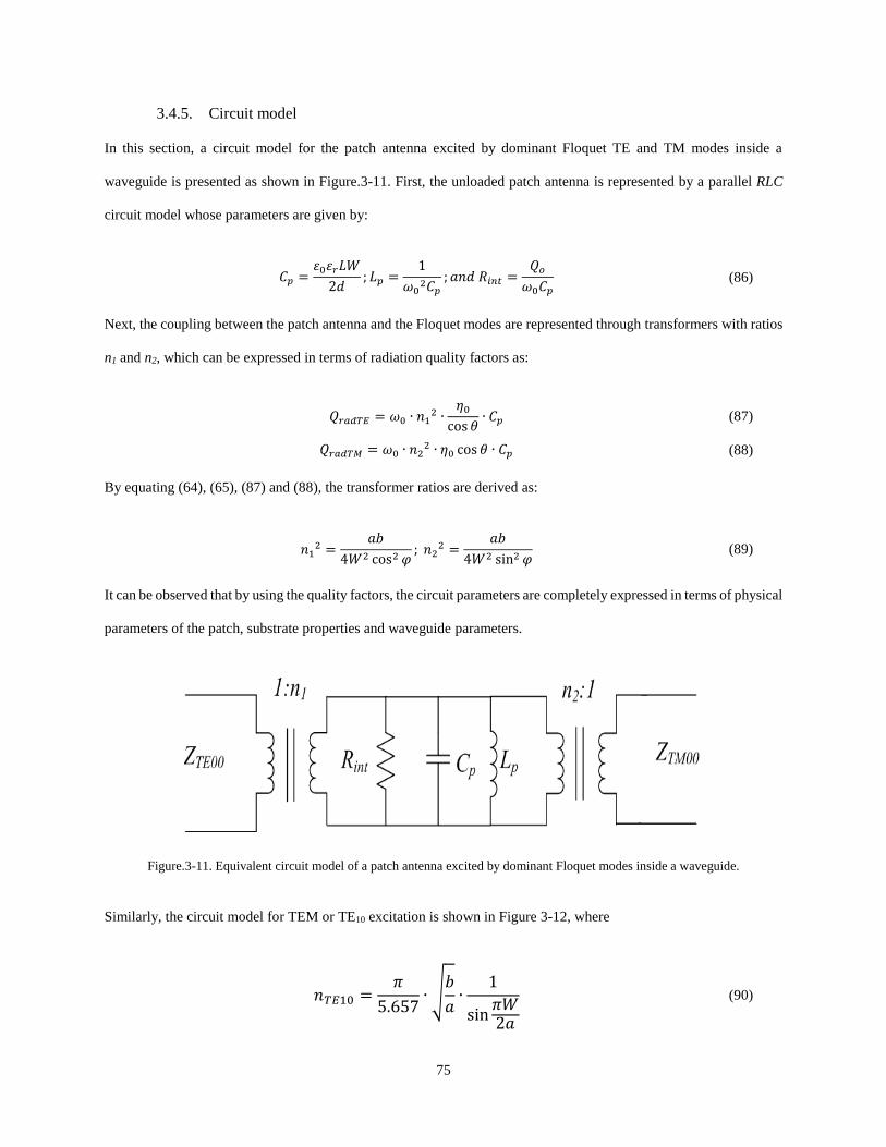
3.4.5. Circuit model ......................................................................................................................................... 75
ix
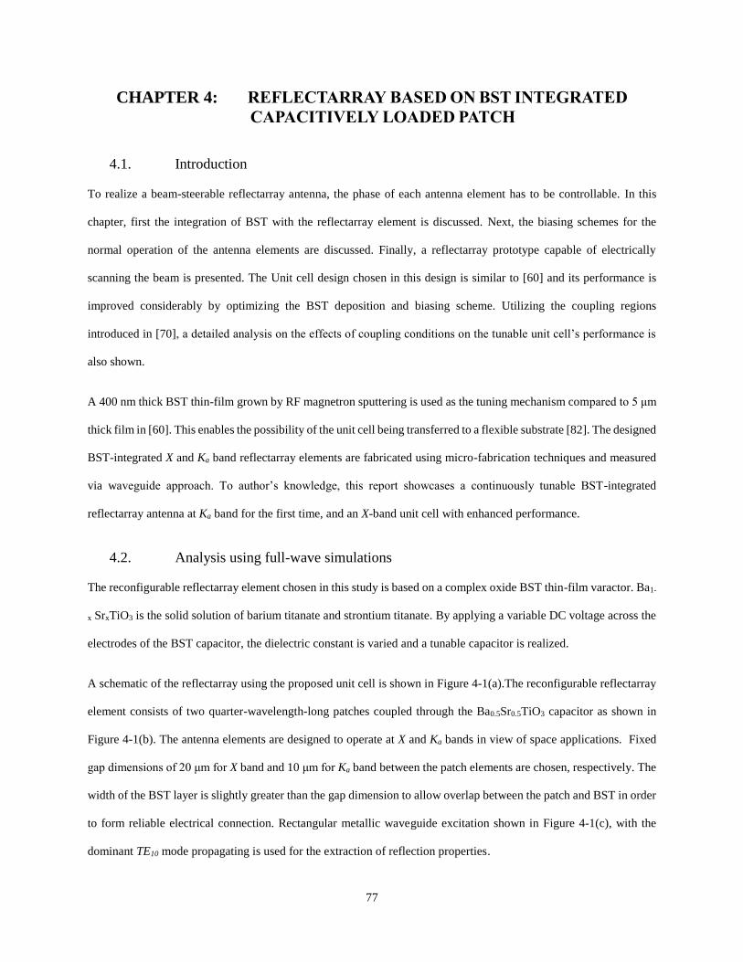
CHAPTER 4: REFLECTARRAY BASED ON BST INTEGRATED CAPACITIVELY LOADED PATCH ... 77
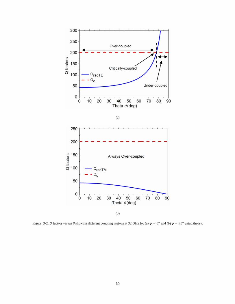
4.2. Analysis using full-wave simulations......................................................................................................... 77
4.3. Unit cell fabrications and measurements .................................................................................................... 89
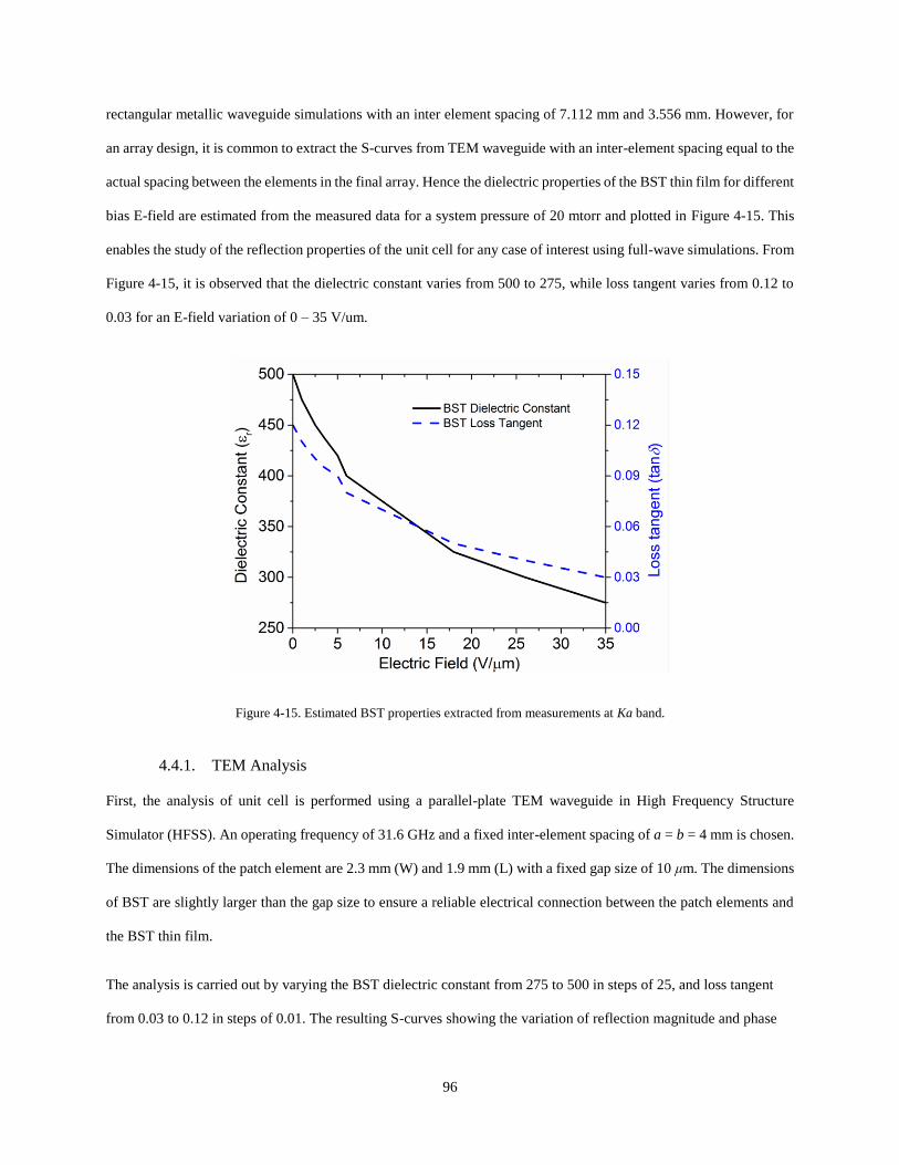
4.4. BST properties and unit cell analysis ......................................................................................................... 95
4.4.1. TEM Analysis ........................................................................................................................................ 96
4.5.2. Array analysis using full-wave simulations ......................................................................................... 101
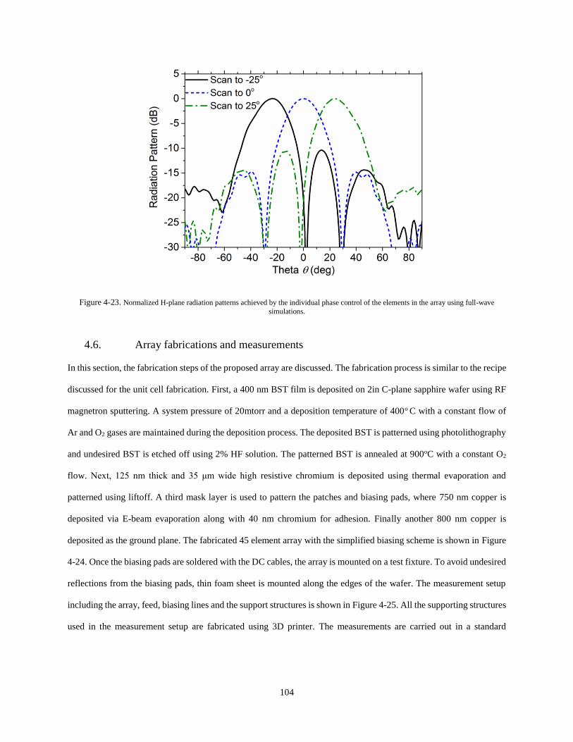
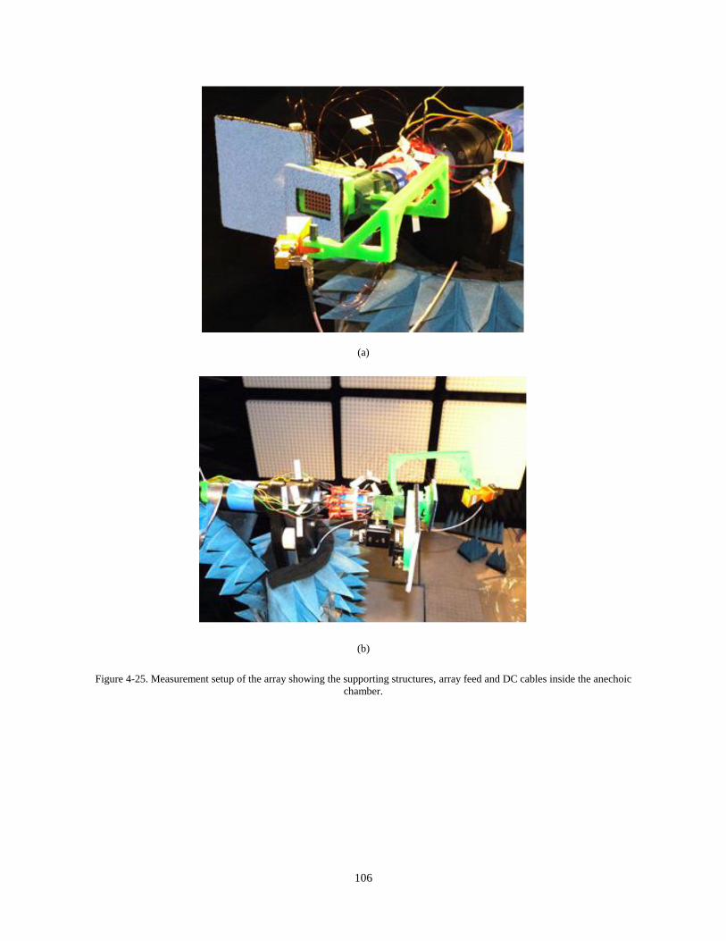
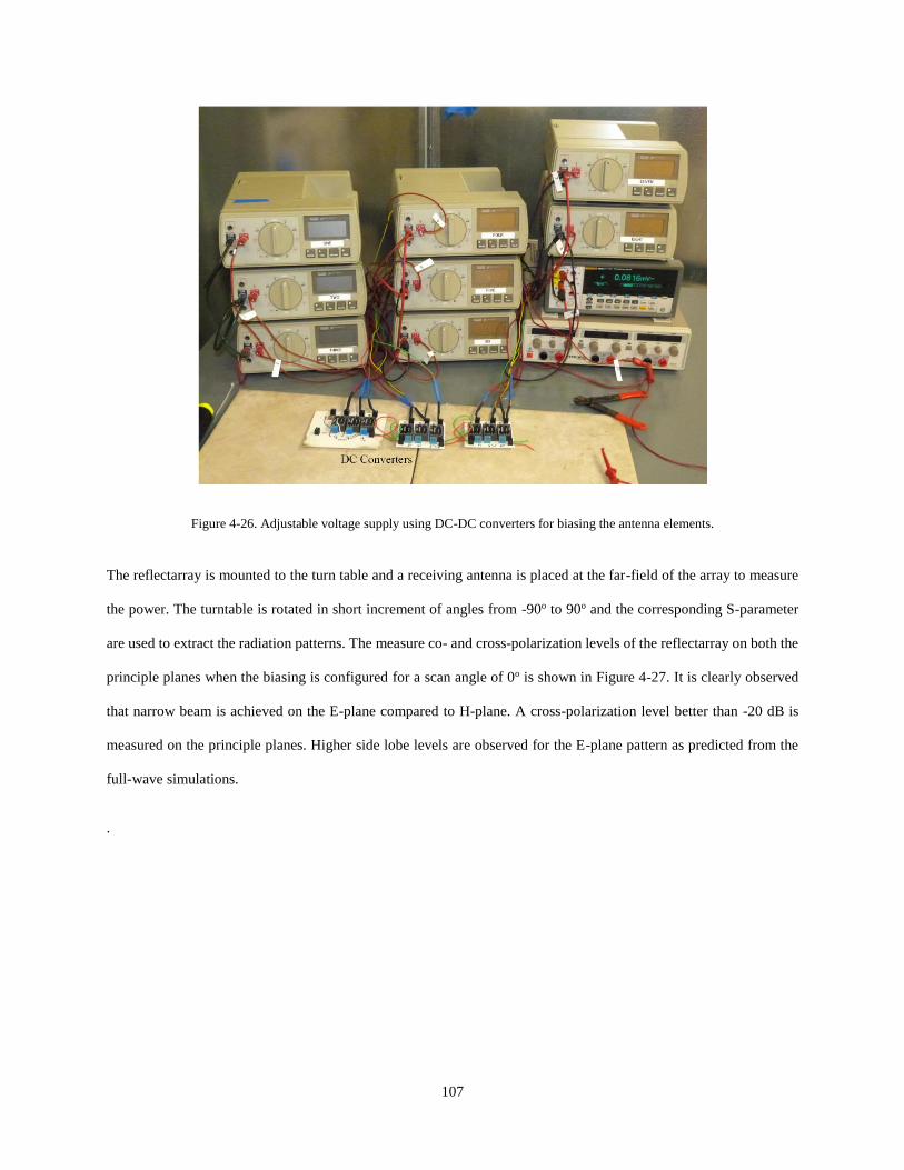
4.6. Array fabrications and measurements ...................................................................................................... 104
FUTURE WORK ...................................................................................................................................................... 111
Figure 1-1. Geometry of a printed reflectarray antenna with an illuminating feed. ....................................................... 3
Figure 1-2. BST’s perovskite crystal structure without external applied electric field. ............................................... 11
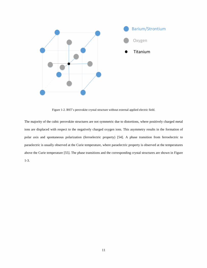
Figure 1-3. Phase transitions and corresponding crystal structure of perovskite ferroelectric materials [56, 57]. ...... 12
Figure 2-1. Waveguide simulator approach for studying a reflectarray unit cell (a) ideal TEM excitation (b) practical
TE10 excitation using metallic walls and (c) the electric field and magnetic current distribution on the reflectarray unit
cell in (a) or (b). ........................................................................................................................................................... 15
Figure 2-2. Q factors versus substrate thickness using the theory. .............................................................................. 22
Figure. 2-3. Reflection (a) magnitude, and (b) phase versus frequency for different h using the theory and full-wave
simulations showing different coupling conditions. .................................................................................................... 23
Figure. 2-4. Reflection magnitude versus substrate thickness at 32 GHz using theory and full-wave simulations. ... 24
Figure. 2-5. Bandwidth and Phase-swing for L/L0 = ±0.2 versus substrate thickness at 32 GHz using theory and full-
Figure. 3-3. (a) Reflection magnitude and (b) phase sensitivity vs. θ at resonance for 𝜑 = 0𝑜 and 𝜑 = 90𝑜 using
theory and HFSS simulations. ..................................................................................................................................... 61
Figure. 3-4. Q factors vs. θ showing coupling regions for (a) TE co-coupled wave component and (b) TM co-coupled
wave component at 32 GHz resonance for 𝜑 = 45𝑜 using theory. ............................................................................. 63
Figure. 3-5. (a) Reflection magnitude and (b) phase sensitivity vs. θ for co-coupled and cross-coupled wave
components at 32 GHz resonance for 𝜑 = 45𝑜 using theory and HFSS simulations. ................................................ 64
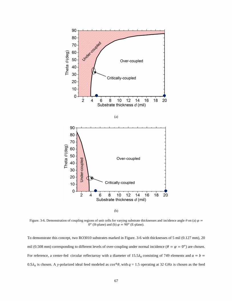
Figure. 3-6. Demonstration of coupling regions of unit cells for varying substrate thicknesses and incidence angle θ
on (a) 𝜑 = 0𝑜 (H-plane) and (b) 𝜑 = 90𝑜 (E-plane). ................................................................................................. 67
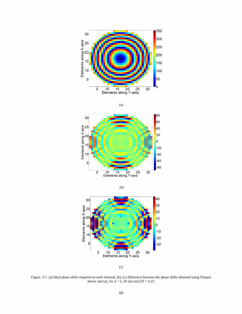
Figure. 3-7. (a) Ideal phase shifts required on each element, (b), (c) difference between the phase shifts obtained using
Floquet theory and (a), for d = 5, 20 mil and f/D = 0.25. ............................................................................................. 69
Figure. 3-8. Reflection magnitude obtained for f/D = 0.25 by considering (a), (b) a fixed normal TEM incidence for d
= 5 and 20 mil substrates. (c), (d) Floquet theory for d = 5 and 20 mil substrates. ..................................................... 71
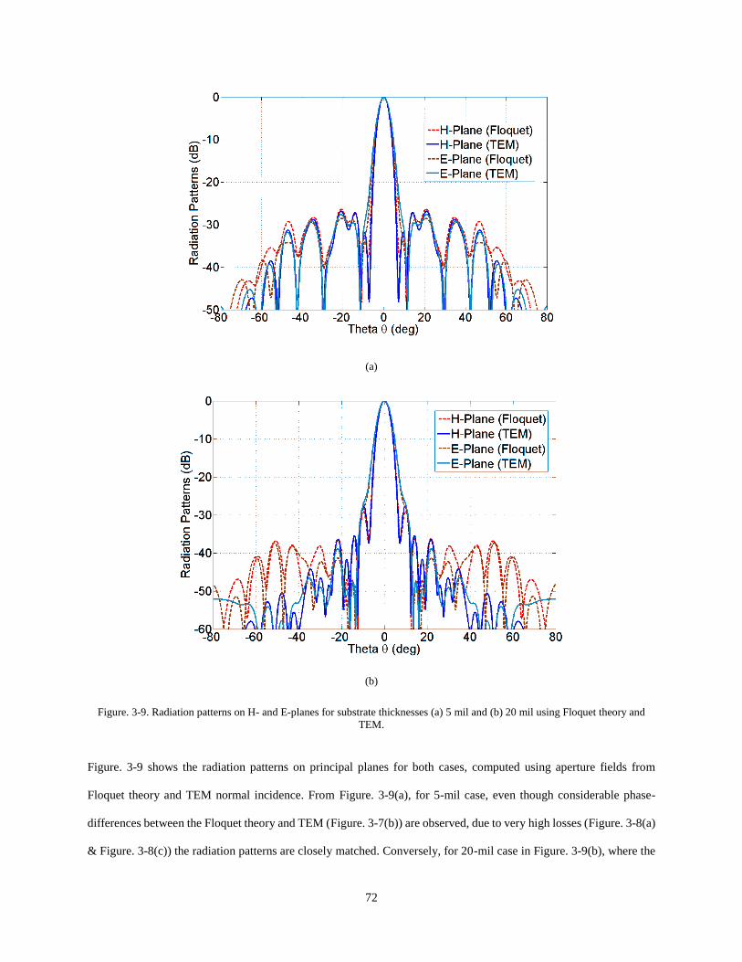
Figure. 3-9. Radiation patterns on H- and E-planes for substrate thicknesses (a) 5 mil and (b) 20 mil using Floquet
theory and TEM. .......................................................................................................................................................... 72
Figure.3-10. Demonstration of coupling regions of unit cells for varying patch widths, dielectric constants, substrate
loss tangents, metal conductivities vs. incidence angle θ on (a), (c), (e), (g) 𝜑 = 0𝑜 (H-plane) and (b), (d), (f), (h) 𝜑 =
Figure.3-11. Equivalent circuit model of a patch antenna excited by dominant Floquet modes inside a waveguide. . 75
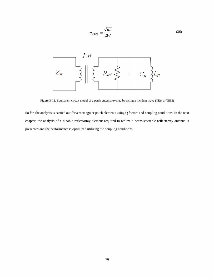
Figure 3-12. Equivalent circuit model of a patch antenna excited by a single incident wave (TE10 or TEM) ............. 76
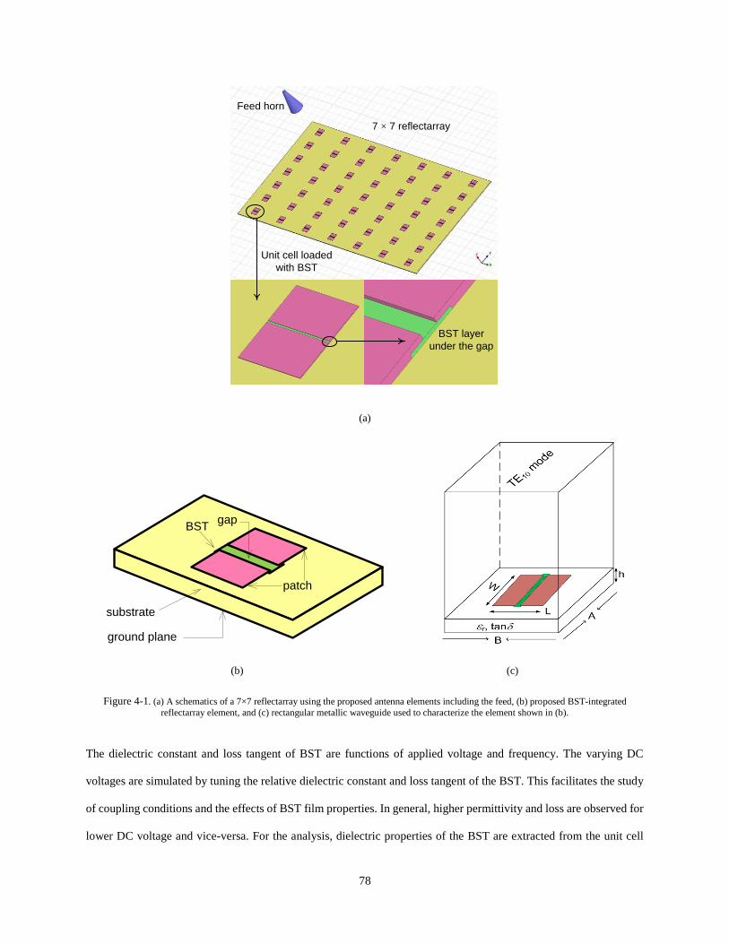
Figure 4-1. (a) A schematics of a 7×7 reflectarray using the proposed antenna elements including the feed, (b) proposed
BST-integrated reflectarray element, and (c) rectangular metallic waveguide used to characterize the element shown
in (b). ........................................................................................................................................................................... 78
xiii
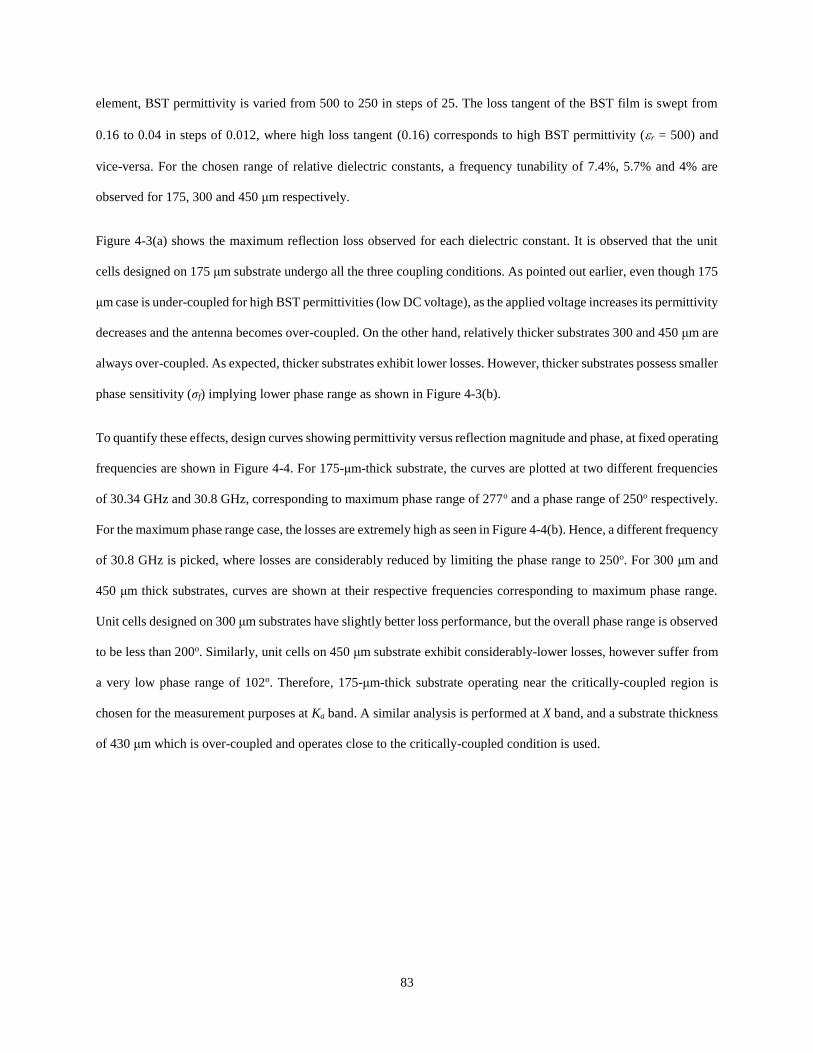
Figure 4-2. (a) Reflection magnitude and (b) phase sensitivity vs. substrate thickness at resonant frequency of the unit
cells showing the coupling regions. ............................................................................................................................. 80
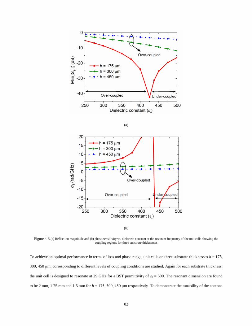
Figure 4-3.(a) Reflection magnitude and (b) phase sensitivity vs. dielectric constant at the resonant frequency of the
unit cells showing the coupling regions for three substrate thicknesses ...................................................................... 82
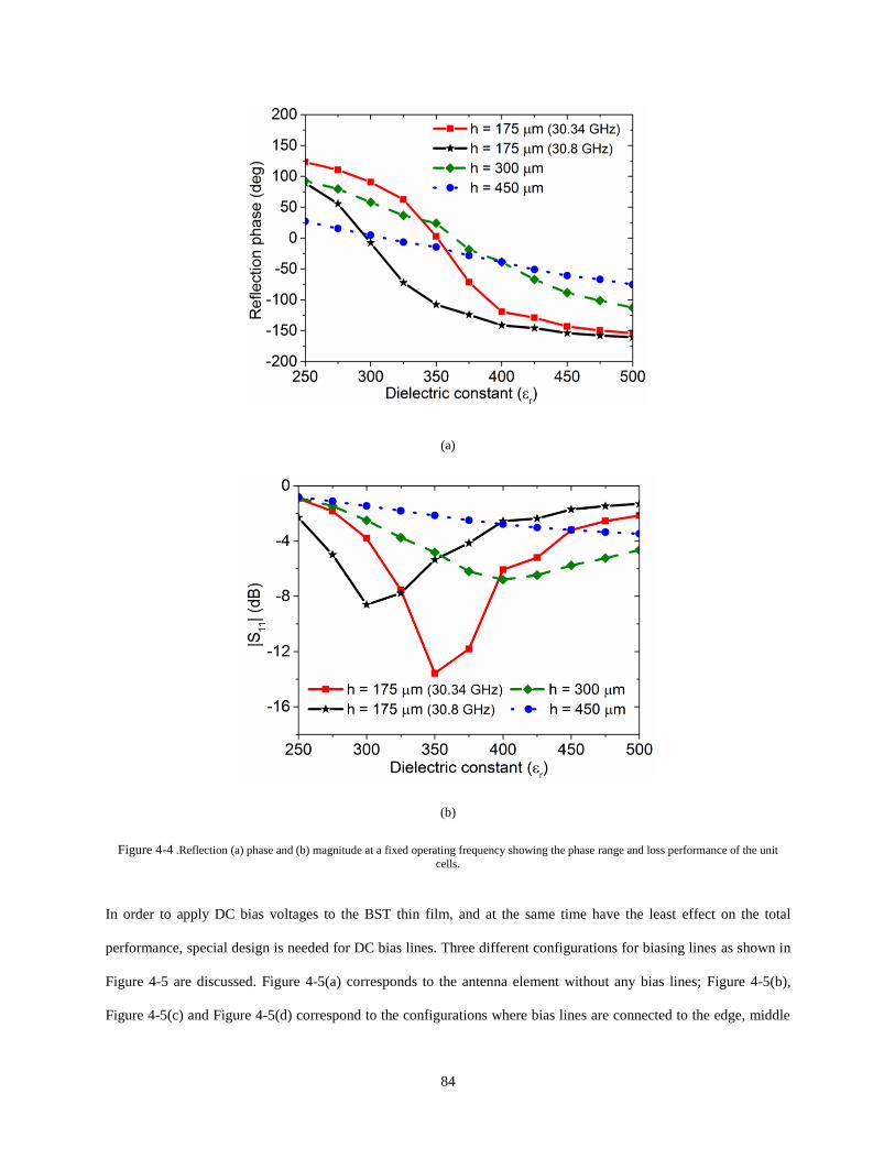
Figure 4-4 .Reflection (a) phase and (b) magnitude at a fixed operating frequency showing the phase range and loss
performance of the unit cells. ...................................................................................................................................... 84
Figure 4-5. Different bias line configurations. (a) No bias lines, (b) horizontal bias lines at the corner of each patch,
(c) horizontal bias lines at the middle of each patch, and (d) horizontal bias lines at the Emin of the patch (1.26mm from
the center of the unit cell). ........................................................................................................................................... 85
Figure 4-6. Current density for different bias lines. (a) No bias lines, (b) horizontal bias lines at the corner of each
patch, (c) horizontal bias lines at the middle of each patch, and (d) horizontal bias lines at the Emin of the patch. ..... 85
Figure 4-7. A reflectarray unit cell loaded with a BST layer acting as a distributed capacitance and corresponding
reflection (a) magnitude and (b) phase for different biasing schemes. ........................................................................ 87
Figure 4-8. (a) Ka-band measurement setup showing the fabricated reflectarray element with the biasing lines, sample
holder and the waveguide adaptor, (b) fabrication steps for the proposed unit cells, (c) Top view of an X-band BST-
based reflectarray unit cell, and (d) measurement setup at X band with the sample holder. ........................................ 89
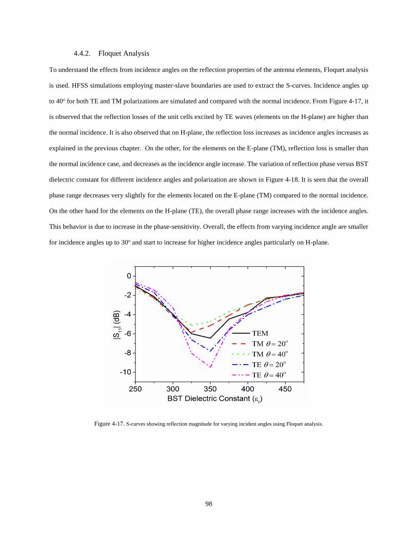
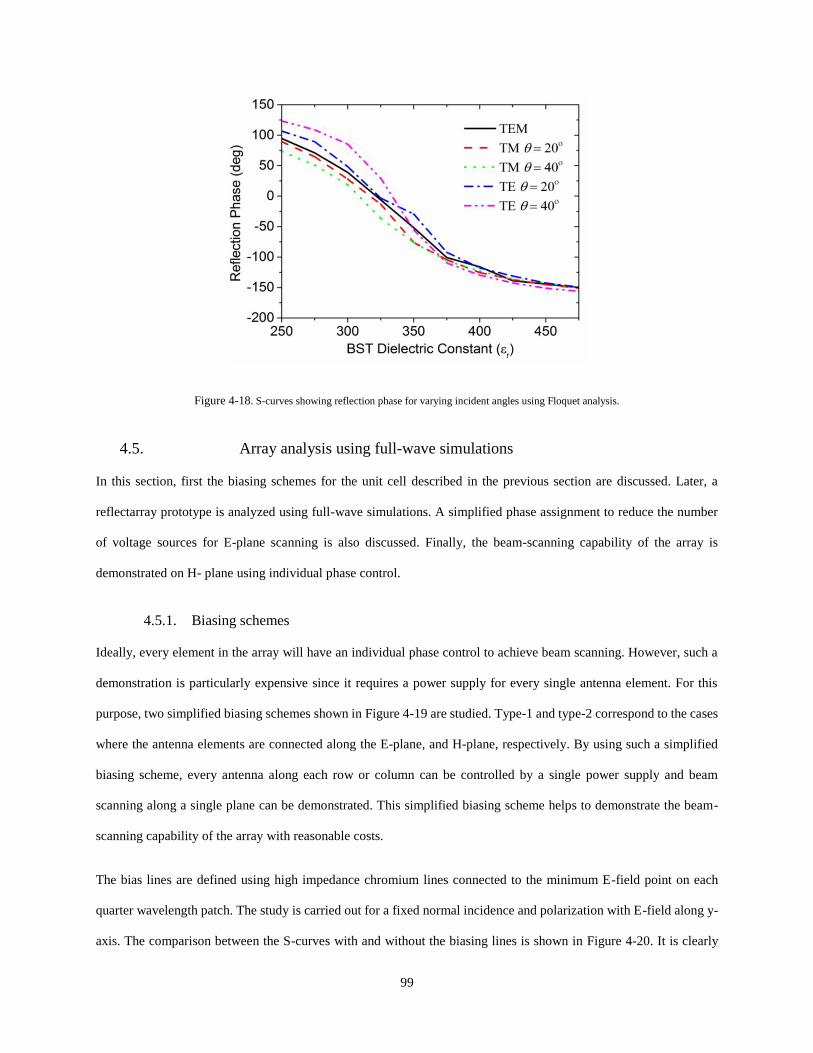
Figure 4-9. Measured reflection magnitude and phase of the unit cells with and without the biasing lines at Ka band.
Figure 4-26. Adjustable voltage supply using DC-DC converters for biasing the antenna elements. ....................... 107
Figure 4-27. Radiation patterns on the principle planes showing both co- and cross- polarization components. ..... 108
Figure 4-28. Radiation patterns for different scan-angles along E-plane. ................................................................. 108
Figure 4-29. Measured gain vs. frequency for broadside radiation pattern. ............................................................... 109
xv
LIST OF TABLES
Table 1-1. Comparison of various reconfigurable technology for the implementation of tunable reflectarrays. (‘+’, ‘0’,
and ‘-‘ refer to good, neutral and poor, respectively. [53] ........................................................................................... 10
Table 4-1. Loss budget of the array for the broadside case ....................................................................................... 109
1
CHAPTER 1: INTRODUCTION
1.1. Motivation
One of the primary interests of 21st century is to understand the Earth and other planets of our solar system, and their
interactions. This knowledge not only helps us understand the world better, but also predict the changes in the future
[1]. These interactions occur from local, regional to global and range from interim weather to enduring climate,
predictable cyclones to unpredictable tsunami and earthquakes, motion of the Earth and other planets, life outside the
Earth etc. For precise characterization of these complex changes in the global system, next-generation tracking systems
are required to be agile, multifunctional, and tunable with high data rates, particularly at frequencies of Ka band and
above. Antenna is one of the major components of a communication system. These antenna systems are able to use a
common aperture for inter- and intra-planet communications, remote sensing, and radar applications. To enable the
rapid and seamless switching between the aforementioned functions, electrically beam-steerable antennas with high
tuning speeds are required. With sophisticated tracking systems and high-pixel cameras on board, antenna systems
with high data rates are crucial to reduce the transmission time of data and high-quality images by more than one order
of magnitude. At the same time, mechanical considerations and high launching costs demand for compact, flexible
and deployable systems.
Parabolic reflectors, though highly efficient and wide band, are bulky and heavy. The complicated curvature makes
reflector antennas expensive in both fabrication and deployment. Phased array antennas, on the other hand, can be
planar and easily deployable. However, they suffer from the disadvantages of complex beam-forming manifold and
expensive transmit/receive modules. Reflectarray antennas, an exquisite combination of reflectors and antenna arrays,
utilize quasi-optical excitation on a planar aperture and are capable of electrically steering the beam without the need
of lossy feed networks.
1.2. Introduction to Reflectarray antennas
Reflectarray antennas have been considered as a promising candidate for highly efficient, directive and beam scanning
applications due to their unique advantage of combining reflectors and antenna arrays [2], [3], [4]. Berry et al first
proposed the concept of reflectarray using waveguide elements [5] as early as 1963. Reflectarray with microstrip
elements was first investigated as early as 1978 [6]. With the advancement in fabrication technology, microstrip
2
reflectarray antennas started to become popular in early 1990’s due to their simple planar geometry and low profile
[7], [8].
A plurality of microwave applications desire highly-directive antennas with the main beam focused at a specified
direction. Reflectors and antenna arrays have been commonly employed to achieve the same goal. Reflector antennas
can provide large bandwidths and high efficiencies, however, are bulky and expensive to fabricate and deploy. On the
other hand, antenna arrays can be planar but suffer from additional losses inside complex feed networks. Reflectarray
antenna is an exquisite solution that combines the advantages of quasi-optical excitation of parabolic reflectors and
planar structure of antenna arrays. Similar to parabolic reflectors, reflectarray antennas can achieve very high
efficiencies (>50 percent). Being flat and compact in form factor similar to phased arrays [9], reflectarray facilitates
an inexpensive fabrication procedure and simpler mechanism to deploy with moderate installation costs. Reflectarray
elements with active phase adjustment capability can provide tunable and beam scanning capabilities. Low profile,
high gain, beam steering capabilities, conformal and compact forms make reflectarrays potential contenders for deep-
space telecommunications and micro-spacecrafts, particularly at frequencies of Ka- and V-band [8, 10]. In addition,
by adjusting the phase of the each element, contour beam shapes can also be achieved [11]. Recently, conformal and
flexible reflectarray antennas started to become popular which could provide cost-effective packaging and launching
for spacecrafts [12].
1.3. Operation
Figure 1-1 shows a reflectarray antenna illuminated by a feed. Each element in the array is excited by the incident
wave coming from the feed at different phases. To achieve a constructive interference in the desired direction, every
element of the array needs to provide the required phase compensating for the differential phase delay from the
illuminating feed and also the linear phase variation required for beam scanning. From the array theory, the phase
shifts desired on the element with coordinates (m,n) for a beam scan angle of (θb,φb) can be calculated using:
In this chapter, the reflection properties of reflectarray elements are analyzed using the Q factor theory. The analysis
is first applied for fixed incidence angle cases. In a reflectarray design, the phase of each antenna element is
compensated to account for the differential spatial lengths from the feed and achieve a desired phase front in the
preferred direction. Thus, the knowledge of the phase response of the unit cell is a paramount for any reflectarray
design. There exist many combinations of physical parameters such as dielectric properties, patch size, substrate
thickness, and spacing between the elements, which could result in the same resonant frequency but with different
reflection properties. The optimum design should make the best use of the aforementioned degrees of freedom in order
to achieve the desired reflectarray performance. Among these parameters, effects of the substrate thickness have been
investigated. It was reported in [66] that as the substrate thickness increases, the reflection loss decreases which is
desirable. However, as this study was further expanded in [67], it was shown that thicker substrates exhibit smaller
phase-swing which limits the reflectarray beam-steering angle. Recently, effects of the substrate loss on the reflection
properties of reflectarray unit cells were reported in [68]. It was observed that for certain combinations of dielectric
losses and substrate thicknesses, the unit cells exhibit anomalous phase-swing phenomenon. Therefore, it is necessary
to study the effects of various physical parameters on the reflectarray unit cell performance such as phase-swing,
bandwidth, and loss. In addition, a theoretical model is desirable to predict and avoid the misbehaved phase responses.
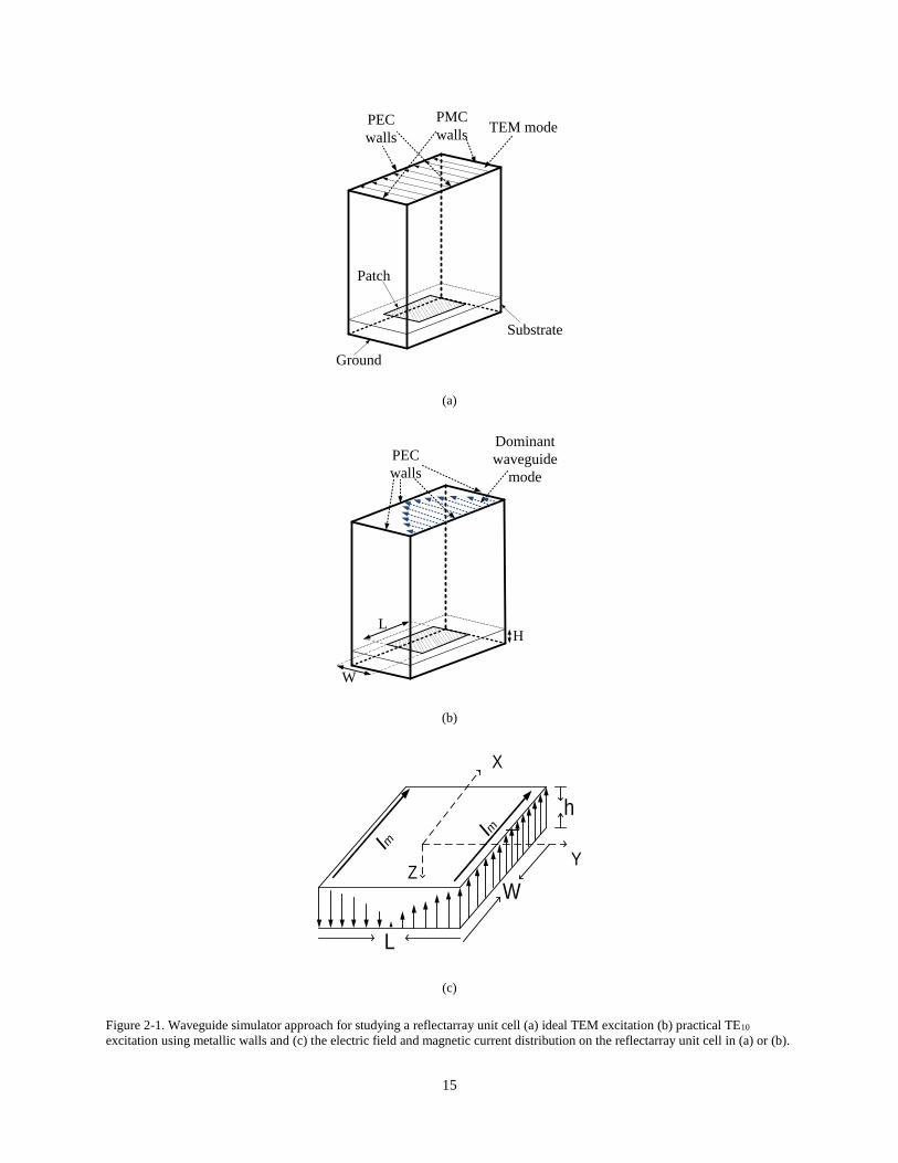
15
(a)
(b)
(c)
Figure 2-1. Waveguide simulator approach for studying a reflectarray unit cell (a) ideal TEM excitation (b) practical TE10
excitation using metallic walls and (c) the electric field and magnetic current distribution on the reflectarray unit cell in (a) or (b).
TEM modePEC
walls
PMC
walls
Patch
Ground
Substrate
Dominant
waveguide
mode
PEC
walls
W
LH
L
W
h
ImIm
X
YZ
16
In this section, an intuitive theoretical expression of the reflection coefficient of reflectarray unit cell is derived using
its analogy to coupled resonators [69, 70].
This theory uses the quality (Q) factors to quantify the reflection characteristics of reflectarray unit cells. In this
approach, there is no need for the intermediate lumped-element circuit model which still relies on full-wave
simulations shown in [40, 71]. Using the theory developed here, the anomalous phase-swing phenomenon [68, 72]
can be identified and avoided in reflectarray designs. Effects of substrate thickness (h), dielectric constant (εr), and
patch width (W), dielectric and metallic losses on the reflection coefficient, phase-swing, and bandwidth are
theoretically derived and verified using full-wave simulations. First, the expressions for reflection coefficients of unit
cell excited by fixed incident angles are discussed. Next, a technique to extract the quality factor using full-wave
simulations is also presented. Later, the difference between TEM and TE10 modes of excitation is analyzed in terms
of Q factors and coupling conditions. Finally, the effects of inter-element spacing on the unit cell’s performance are
shown.
2.2. Theoretical approach
Waveguide excitation is commonly used to characterize and design reflectarray unit cells. In this approach, the
reflectarray unit cell is placed inside a parallel-plate TEM waveguide as shown in Figure 2-1(a) or a rectangular
metallic waveguide as shown in Figure 2-1(b) and the reflection properties of the unit cell are extracted. This method
uses periodic boundaries to simulate an infinite reflectarray accounting for the mutual coupling. A parallel-plate TEM
waveguide corresponds to a plane wave with fixed normal incidence. On the other hand, a rectangular waveguide
corresponds to an oblique incidence angle that is dependent on the frequency of operation and waveguide dimensions.
The TEM waveguide approach is generally limited to simulations as the structure is practically complicated. However,
a metallic rectangular waveguide supporting a TE10 mode is commonly employed for measurements.
In this section, a complete theoretical approach to extract the reflection properties of a unit cell is discussed. The
reflection coefficient at the patch surface for a reflectarray element inside a waveguide can be expressed by coupled
mode theory as [69]:
17
r
r
r
r
f
ffj
QQ
f
ffj
QQ
orad
oradf
2
2
11
11
)( (2)
where fr is the resonant frequency and Qrad is the radiation Q factor of the patch antenna. Qo is the parallel combination
of metallic loss (Qc) and dielectric loss (Qd) of the patch antenna given by [73, 74]:
fhQc
(3)
tan
1dQ
(4)
dc
dco
QQ
QQQ
(5)
First, a theoretical approach to obtain the radiation Q factor of a reflectarray unit cell is presented. For comparison
purposes, a second method which is dependent on simulations [75] is also discussed. First, the expression for Qrad of
a unit cell inside a rectangular waveguide is discussed. The results obtained from theory are compared with
simulations. Using the derived theory, different types of coupling modes for a reflectarray unit cell are discussed. A
few cases are chosen for fabrications and the results obtained from theory, and simulations are compared with
measurements. Along the discussion, the limitations of the model will be discussed with supporting examples.
Similarly, the expression of Qrad for a unit cell inside a parallel-plate TEM waveguide is also shown. A few cases are
chosen and compared with simulations.
2.2.1. Qrad of a rectangular unit cell inside a metallic waveguide:
The reflectarray unit cell inside the waveguide involves two different modes which are coupled together; TM010 mode
resonating inside the patch and TE10 mode propagating inside the waveguide. To formulate the coupling between these
two modes, the structure shown in Figure 2-1(b) can be modeled by a transmission line (the waveguide) terminated
with a resonator (the patch).
18
Qrad is obtained by assuming the reflectarray unit cell as a patch antenna, where the source of excitation is a rectangular
waveguide. An analysis based on the cavity model of a patch is used. Assuming that the dominant mode within the
cavity is TM010 mode, the field distribution under the patch is given by [73]:
2,
2 sin)( 0
Ly
Wx
L
yEyEz
(6)
where 𝐸0 is the electric field amplitude at the radiating edges. L and W are the length and width of the patch
respectively.
Utilizing field equivalence principle, the patch antenna is replaced with equivalent magnetic currents at its radiating
edges as shown in Figure 2-1(c). Using image theory, and assuming a thin cavity, the equivalent magnetic currents
are doubled and are now free to radiate in an infinite waveguide. The linear equivalent magnetic currents at the
radiating edges are [73]:
2,
2 , ˆ2 0
LLyxhEI m (7)
At the non-radiating edges, we have:
2/ , ˆsin2)( 0 WxyL
yhEyI m
(8)
The amplitude A+ of TE10 mode excited in the infinite waveguide by a volume magnetic current density can be
found using [74]:
dvMH
PA
.
11
1
(9)
where 𝐻1 is the magnetic field of the TE10 mode propagating in the negative z direction and P1 is the normalization
constant given by:
WZ
abdszheP ˆ.2 111
(10)
where a and b are the waveguide dimensions and ZW is the wave impedance of the TE10 mode. e1 and h1 are the modal
transverse field components of the TE10 mode given by [74]:
19
a
xye
sinˆ
1 (11)
a
x
Z
xh
W
sin
ˆ1
(12)
and 𝑍𝑊 is given by:
22
ac
ZW
W
(13)
Noting that only the radiating edges contribute to the integral in (9), it simplifies to a line integral. Using 𝐼 in place
of in (9), A+ is found as:
)2
sin(8 0
a
W
b
hEA
(14)
The power carried away by the TE10 mode towards the waveguide port is:
)2
(sin16
4
2
1
2
2
2
0
22
*
a
W
bZ
aEhA
Z
ab
dsHEP
WW
rad
(15)
The electric energy stored in the patch is given by:
hWLEdvEWe
2
0
2
8
4
(16)
where ε is the permittivity of the substrate material. Since the electric and magnetic energies are equal at resonance,
the external quality factor Qrad is given by:
a
bZ
a
W
LW
h
f
P
StoredEnergyfQ
W
rad
rad
)2
(sin
32
2
2
3
0
0
(17)
where W and L are width and length of the patch, h is the substrate thickness, a and b are the waveguide dimensions
and Zw is the wave impedance of the TE10 mode.
20
2.2.2. Coupling conditions
Using the expressions obtained for Qo and Qrad, the reflection coefficient at the resonant frequency can be
derived using (2):
orad
orad
QQ
QQ
rf
11
11
)(
(18)
It is observed that based on the relative values of Qrad and Qo, three different conditions exist;
1. Qrad = Qo ; Critically-coupled
2. Qrad > Qo ; Under-coupled
3. Qrad < Qo ; Over-coupled
1) If Qrad = Qo, (2) reduces to
0)( r
f (19)
This corresponds to critically-coupled condition. In this case there is no reflection from the unit cell and all the energy
is dissipated inside the resonator. This condition is not useful for reflectarray applications.
2) If Qrad > Qo,
je
rf
rf )()( (20)
This corresponds to under-coupled condition. At this condition, it can be observed that the reflection phase at
resonance is always 180o, which represents anomalous phase phenomenon.
3) If Qrad < Qo,
0)()(
je
rf
rf (21)
This corresponds to over-coupled condition, which should be used for reflectarray designs.
2.2.3. Reflection loss, Phase-swing and Bandwidth
The effects from h, εr, and W on the performance of the unit cell are evaluated in terms of maximum reflection loss,
phase-swing (Δ), and bandwidth (β), which can be quantified using the Q factors described earlier.
The reflection phase of a unit cell is defined as:
21
orad
r
r
orad
r
r
r
QQ
f
ff
QQ
f
ff
ff11
2
tan11
2
tan),( 11 (22)
Phase-swing is defined as:
),(),( 1020 ffff (23)
0
02
0
01
1 ;
1 LL
ff
LL
ff
(24)
where f0 is the center frequency of the reflectarray unit cell. L0 is the patch length to achieve a resonant frequency
equal to f0. f1 and f2 correspond to the resonant frequencies by tailoring the patch length L0 with an amount of ±δL.
Bandwidth is defined as the range of frequencies over which the reflection phase differs by ±45o with respect to the
center frequency f0 [71] and can be derived as:
ff
2/1
0
(25)
22
0
2
0 4,
0 rado
rado
ff
fQQf
QQ
f
ff
(26)
2.3. Analysis of coupling conditions and its effects of unit cell’s performance
The response of a unit cell is determined by the combined effect of the physical parameters on Q factors and their
relative values. In this section, the effects of h, W, r, tan, and σ on Q factors, coupling conditions and reflection
properties are studied using the theory defined in Section 2.2. and compared with Ansoft High Frequency Structure
Simulator (HFSS) full-wave simulations.
2.3.1. Effects of Substrate thickness (h)
In this section, unit cells with different substrate thicknesses are studied, while the substrate material (Rogers RO3010
with specified r = 10.2, tan = 0.0035, ½ oz copper) and patch width (W = 2 mm) are fixed. To facilitate adequate
waveguide measurements of unit cells, a high dielectric constant is chosen. The patch length L0 is adjusted to resonate
at 32 GHz for every thickness [73]. Substrate thicknesses h ranging from 1 mil (25.4 µm) to 20 mil (0.508 mm) are
considered for the study. Throughout the text, h is referred in mil in view of commercially-available units. Q factors
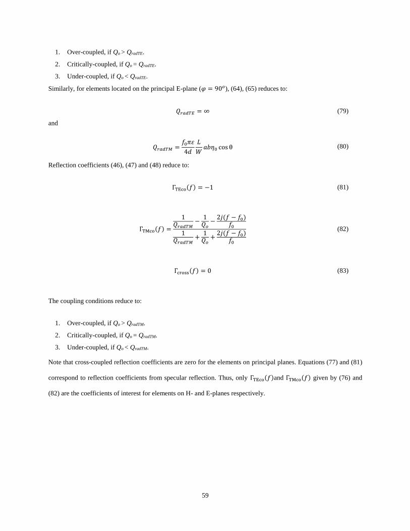
are plotted in Figure 2-2 using the theory described in section 2.2. It is observed that as h increases, Qo increases
22
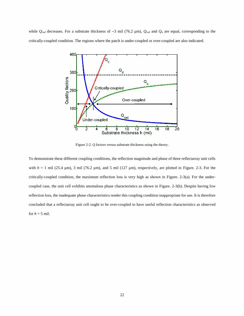
while Qrad decreases. For a substrate thickness of 3 mil (76.2 µm), Qrad and Qo are equal, corresponding to the
critically-coupled condition. The regions where the patch is under-coupled or over-coupled are also indicated.
Figure 2-2. Q factors versus substrate thickness using the theory.
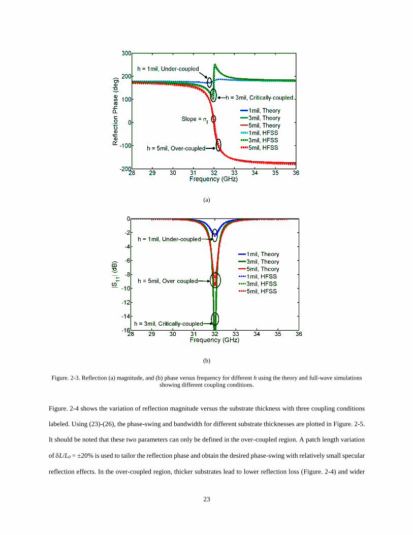
To demonstrate these different coupling conditions, the reflection magnitude and phase of three reflectarray unit cells
with h = 1 mil (25.4 µm), 3 mil (76.2 µm), and 5 mil (127 µm), respectively, are plotted in Figure. 2-3. For the
critically-coupled condition, the maximum reflection loss is very high as shown in Figure. 2-3(a). For the under-
coupled case, the unit cell exhibits anomalous phase characteristics as shown in Figure. 2-3(b). Despite having low
reflection loss, the inadequate phase characteristics render this coupling condition inappropriate for use. It is therefore
concluded that a reflectarray unit cell ought to be over-coupled to have useful reflection characteristics as observed
for h = 5 mil.
23
(a)
(b)
Figure. 2-3. Reflection (a) magnitude, and (b) phase versus frequency for different h using the theory and full-wave simulations
showing different coupling conditions.
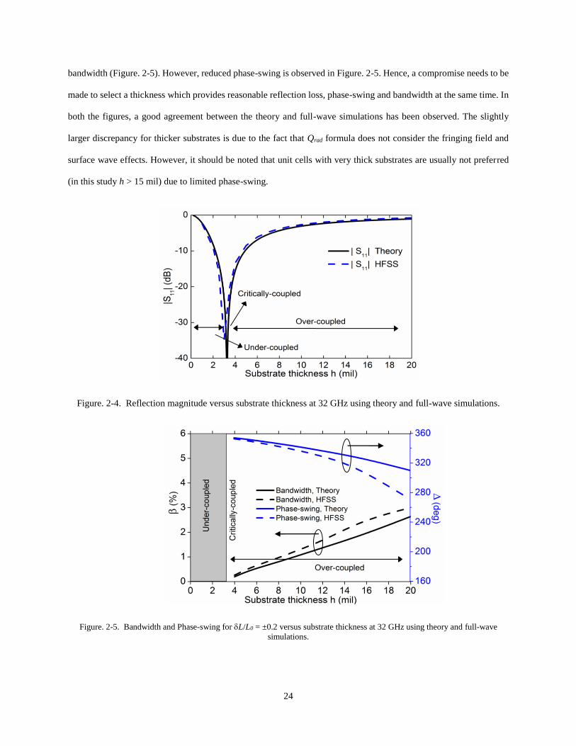
Figure. 2-4 shows the variation of reflection magnitude versus the substrate thickness with three coupling conditions
labeled. Using (23)-(26), the phase-swing and bandwidth for different substrate thicknesses are plotted in Figure. 2-5.
It should be noted that these two parameters can only be defined in the over-coupled region. A patch length variation
of L/L0 = ±20% is used to tailor the reflection phase and obtain the desired phase-swing with relatively small specular
reflection effects. In the over-coupled region, thicker substrates lead to lower reflection loss (Figure. 2-4) and wider
24
bandwidth (Figure. 2-5). However, reduced phase-swing is observed in Figure. 2-5. Hence, a compromise needs to be
made to select a thickness which provides reasonable reflection loss, phase-swing and bandwidth at the same time. In
both the figures, a good agreement between the theory and full-wave simulations has been observed. The slightly
larger discrepancy for thicker substrates is due to the fact that Qrad formula does not consider the fringing field and
surface wave effects. However, it should be noted that unit cells with very thick substrates are usually not preferred
(in this study h > 15 mil) due to limited phase-swing.
Figure. 2-4. Reflection magnitude versus substrate thickness at 32 GHz using theory and full-wave simulations.
Figure. 2-5. Bandwidth and Phase-swing for L/L0 = ±0.2 versus substrate thickness at 32 GHz using theory and full-wave
simulations.
25
2.3.2. Effects of Patch width (W)
Figure. 2-6 shows Q factors, reflection loss, phase-swing, and bandwidth versus patch width for the same substrate
material with a thickness of 5 mil, and at 32 GHz. It is observed in Figure. 2-6(a) that Qrad is the only Q factor
depending on W. All three coupling regions are labeled. In the over-coupled region, as W increases, the reflection loss
decreases and bandwidth increases, but at the expense of reduced phase-swing. Good agreement between theory and
full-wave simulation is observed, particularly in the over-coupled region, which is the region of interest in reflectarray
design. A difference of 0.3 mm (0.03λ0) in the value of W corresponding to critical coupling is primarily due to the
pronounced effect from the fringing field; this is especially true for narrow patches. However, it should be noted that
the under-coupled region needs to be avoided in the reflectarray design.
2.3.3. Effects of Dielectric Constant (r)
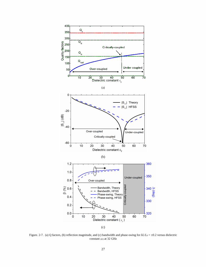
In this subsection, the effects from r on reflection properties of reflectarray unit cells are studied. Figure. 2-7 shows
Q factors, reflection loss, phase-swing, and bandwidth versus dielectric constant for unit cells having patch width of
2 mm, substrate thickness of 5 mil, and loss tangent of 0.0035, at 32 GHz. It is observed that the only Q factor
depending on dielectric constant is Qrad. Critical coupling is observed at r 49, which is beyond the conventional
range of dielectric constants (2.2 ≤ r ≤ 12). Thus for the chosen unit cells, any practical dielectric thickness can be
chosen to ensure the over-coupled case. In the over-coupled region, as r decreases, the reflection loss decreases and
the bandwidth increases, again with a reduced phase-swing. The theory matches the full-wave simulations very well,
particularly in the useful over-coupled region. The discrepancy in r corresponding to the critical coupling is mainly
from the surface wave effects.
26
(a)
(b)
(c)
Figure. 2-6. (a) Q factors, (b) reflection magnitude, and (c) bandwidth and phase-swing for L/L0 = ±0.2 versus patch width (W)
at 32 GHz.
27
(a)
(b)
(c)
Figure. 2-7. (a) Q factors, (b) reflection magnitude, and (c) bandwidth and phase-swing for L/L0 = ±0.2 versus dielectric
constant (r) at 32 GHz
28
2.3.4. Effects of Dielectric and Metallic Losses
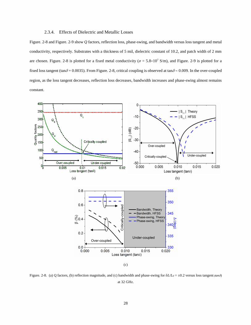
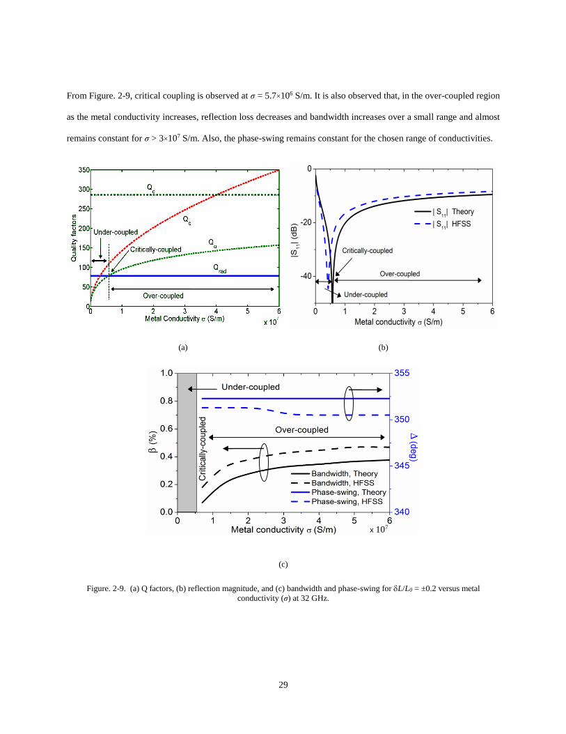
Figure. 2-8 and Figure. 2-9 show Q factors, reflection loss, phase-swing, and bandwidth versus loss tangent and metal
conductivity, respectively. Substrates with a thickness of 5 mil, dielectric constant of 10.2, and patch width of 2 mm
are chosen. Figure. 2-8 is plotted for a fixed metal conductivity (σ = 5.8×10⁷ S/m), and Figure. 2-9 is plotted for a
fixed loss tangent (tan = 0.0035). From Figure. 2-8, critical coupling is observed at tan 0.009. In the over-coupled
region, as the loss tangent decreases, reflection loss decreases, bandwidth increases and phase-swing almost remains
constant.
(a) (b)
(c)
Figure. 2-8. (a) Q factors, (b) reflection magnitude, and (c) bandwidth and phase-swing for L/L0 = ±0.2 versus loss tangent (tan)
at 32 GHz.
29
From Figure. 2-9, critical coupling is observed at σ = 5.7×10⁶ S/m. It is also observed that, in the over-coupled region
as the metal conductivity increases, reflection loss decreases and bandwidth increases over a small range and almost
remains constant for σ > 3×10⁷ S/m. Also, the phase-swing remains constant for the chosen range of conductivities.
(a) (b)
(c)
Figure. 2-9. (a) Q factors, (b) reflection magnitude, and (c) bandwidth and phase-swing for L/L0 = ±0.2 versus metal
conductivity (σ) at 32 GHz.
x 107
30
2.3.5. Combined Effects of Different Parameters
In the previous subsections, the effects from each physical parameter are studied, while the other parameters are fixed.
By doing so, contributions from h, W, r, tan, and σ on the unit cell performance were studied separately. It is shown
that there exists a certain value for each parameter which results in critical coupling. However, this position shifts if
any other parameters are changed. To demonstrate this concept, combined effects from dielectric thickness and other
four parameters on the location of critical coupling are studied herein.
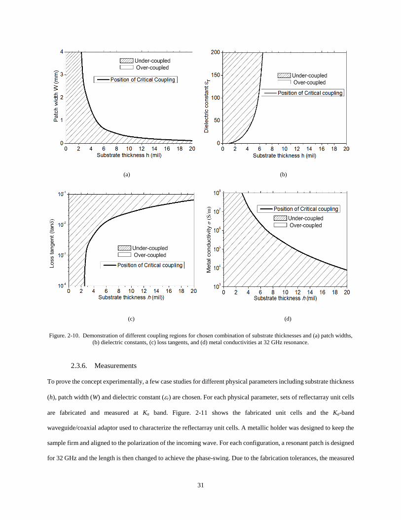
Figure. 2-10(a) shows the location of critical coupling for different substrate thicknesses and patch widths for a fixed
substrate material (r = 10.2, tan = 0.0035, ½ oz copper) and resonant frequency of 32 GHz. It is observed that for
different values of W, the values of h which result in critical coupling are different. As the substrate thickness increases,
the ranges of useful patch widths increases and vice-versa. Similar demonstration is performed for the other three
combinations in Figure. 2-10(b)-(d).
Figure. 2-10(b) is plotted for fixed resonant frequency of f0 = 32 GHz, W = 2 mm, tan = 0.0035 and ½ oz copper. It
is observed that as the dielectric constant increases, the choice of useful substrate thicknesses decreases. In addition,
for this particular combination, all commercially-available dielectric constants fall in the over-coupled range for
h>4mil. Figure. 2-10(c) and Figure. 2-10(d) are plotted for substrates with a dielectric constant of 10.2, and patch
width of 2 mm, resonating at 32 GHz. Figure. 2-10(c) is plotted for a fixed metal conductivity (σ = 5.8×10⁷ S/m), and
Figure. 2-10(d) is plotted for a fixed loss tangent (tan = 0.0035). It is observed that as the dielectric loss increases or
metal conductivity decreases, the choice of substrate thicknesses which correspond to over-coupled region decreases.
It is also observed that the unit cell is always under-coupled for σ < 104 S/m. The results of this subsection suggest
simultaneous investigation of different physical parameters and serves as guideline for unit cell performance
optimization.
31
(a) (b)
(c) (d)
Figure. 2-10. Demonstration of different coupling regions for chosen combination of substrate thicknesses and (a) patch widths,
(b) dielectric constants, (c) loss tangents, and (d) metal conductivities at 32 GHz resonance.
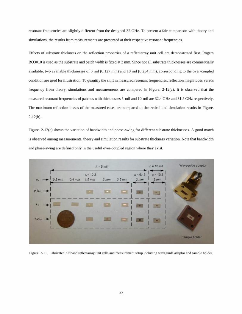
2.3.6. Measurements
To prove the concept experimentally, a few case studies for different physical parameters including substrate thickness
(h), patch width (W) and dielectric constant (r) are chosen. For each physical parameter, sets of reflectarray unit cells
are fabricated and measured at Ka band. Figure. 2-11 shows the fabricated unit cells and the Ka-band
waveguide/coaxial adaptor used to characterize the reflectarray unit cells. A metallic holder was designed to keep the
sample firm and aligned to the polarization of the incoming wave. For each configuration, a resonant patch is designed
for 32 GHz and the length is then changed to achieve the phase-swing. Due to the fabrication tolerances, the measured
32
resonant frequencies are slightly different from the designed 32 GHz. To present a fair comparison with theory and
simulations, the results from measurements are presented at their respective resonant frequencies.
Effects of substrate thickness on the reflection properties of a reflectarray unit cell are demonstrated first. Rogers
RO3010 is used as the substrate and patch width is fixed at 2 mm. Since not all substrate thicknesses are commercially
available, two available thicknesses of 5 mil (0.127 mm) and 10 mil (0.254 mm), corresponding to the over-coupled
condition are used for illustration. To quantify the shift in measured resonant frequencies, reflection magnitudes versus
frequency from theory, simulations and measurements are compared in Figure. 2-12(a). It is observed that the
measured resonant frequencies of patches with thicknesses 5-mil and 10-mil are 32.4 GHz and 31.5 GHz respectively.
The maximum reflection losses of the measured cases are compared to theoretical and simulation results in Figure.
2-12(b).
Figure. 2-12(c) shows the variation of bandwidth and phase-swing for different substrate thicknesses. A good match
is observed among measurements, theory and simulation results for substrate thickness variation. Note that bandwidth
and phase-swing are defined only in the useful over-coupled region where they exist.
Figure. 2-11. Fabricated Ka band reflectarray unit cells and measurement setup including waveguide adaptor and sample holder.
33
Figure. 2-12. (a) Reflection magnitude versus frequency (b) reflection magnitude versus substrate thickness (fixed W and r), (c)
bandwidth and phase-swing versus substrate thickness using theory, HFSS and measurements
(a)
(c)
(b)
34
Effects of patch width on reflection properties are demonstrated in Figure. 2-13. Unit cells with patch widths of 0.2,
0.4, 1.5, 2 and 3.5 mm are fabricated on a 5-mil-thick RO 3010 substrate. Patch widths of 0.2 and 0.4 mm fall in the
under-coupled condition while others correspond to over-coupled region. Reflection magnitude versus frequency for
the over-coupled patches is shown in Figure. 2-13(a). Again for comparison, maximum reflection loss is plotted in
Figure. 2-13(b), and bandwidth, phase-swing are plotted in Figure. 2-13(c). A good agreement, in particular for
bandwidth and phase-swing, is observed between the measurements, theory and simulation results.
Finally, effects of dielectric constant on reflection properties of reflectarray unit cells are presented through
measurements along with theoretical and simulated results in Figure. 2-14. 5-mil-thick Rogers RT6006 and RO3010
with dielectric constants of 6.15 and 10.2, respectively, are chosen for measurement purposes. Patch width of the unit
cells is fixed at 2 mm. Figure. 2-14(a) shows the reflection magnitude versus frequency for 5-mil-thick Rogers RT6006
with tan = 0.0019. Figure. 2-14(b)-(c) shows the measured variation of maximum reflection loss, bandwidth, and
phase-swing versus dielectric constant along with theory and simulations. Note that in Figure. 2-14(b)-(c), the results
from theory and simulations are plotted for a fixed tan = 0.0035. It is observed that the measured data points closely
follow the two traces corresponding to simulations and theory.
35
Figure. 2-13. (a) Reflection magnitude versus frequency, (b) reflection magnitude versus patch width (fixed h and r), (c)
bandwidth and phase-swing versus patch width using theory, HFSS and measurements.
(a)
(c)
(b)
36
Figure. 2-14. (a) Reflection magnitude versus frequency, (b) reflection magnitude versus dielectric constant (fixed h and W), (c)
bandwidth and phase-swing versus dielectric constant using theory, HFSS and measurements.
(a)
(b)
(c)
(c)
37
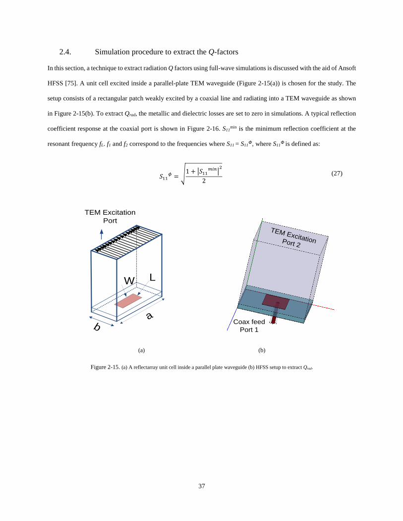
2.4. Simulation procedure to extract the Q-factors
In this section, a technique to extract radiation Q factors using full-wave simulations is discussed with the aid of Ansoft
HFSS [75]. A unit cell excited inside a parallel-plate TEM waveguide (Figure 2-15(a)) is chosen for the study. The
setup consists of a rectangular patch weakly excited by a coaxial line and radiating into a TEM waveguide as shown
in Figure 2-15(b). To extract Qrad, the metallic and dielectric losses are set to zero in simulations. A typical reflection
coefficient response at the coaxial port is shown in Figure 2-16. S11min is the minimum reflection coefficient at the
resonant frequency fL. f1 and f2 correspond to the frequencies where S11 = S11Φ, where S11
Φ is defined as:
𝑆11𝜙 = √1 + |𝑆11
𝑚𝑖𝑛|2
2
(27)
(a) (b)
Figure 2-15. (a) A reflectarray unit cell inside a parallel plate waveguide (b) HFSS setup to extract Qrad.
a
W L
TEM Excitation
Port
b
TEM Excitation Port 2
Coax feed
Port 1
38
Figure 2-16. Reflection coefficient at the coaxial port on a linear scale.
Depending on the location of the coaxial feed, the amount of energy coupled from the coaxial feed to the patch antenna
will be identified. The loaded Q, taking into account the effects of external coaxial feed and measured at the coaxial
port can be defined as [76]:
𝑄𝐿 =𝑓𝐿
𝑓2 − 𝑓1
(28)
In order to calculate the unloaded Q of the patch, which is equal to the radiation Q, the following coupling coefficient
is used [76] :
𝑘 =1 ∓ 𝑆11
𝑚𝑖𝑛
1 ± 𝑆11𝑚𝑖𝑛
(𝑢𝑛𝑑𝑒𝑟𝑐𝑜𝑢𝑝𝑙𝑒𝑑/𝑜𝑣𝑒𝑟𝑐𝑜𝑢𝑝𝑙𝑒𝑑) (29)
Finally, Qrad can be calculated using:
𝑄𝑟𝑎𝑑 = (1 + 𝑘)𝑓𝐿
𝑓2 − 𝑓1
(30)
To demonstrate the validity of the proposed approach, reflection coefficient of a unit cell derived using the presented
theory is compared with HFSS full-wave simulations. A 32 GHz rectangular patch of L × W (1.3 × 2 mm2) is designed
on a 10-mil-thick Rogers RO3010 substrate (r = 10.2, tan = 0.0035). The air-filled coaxial feed is positioned at the
center of the patch along the x-axis and is offset by 0.125 mm from the center along the y-axis. The radiuses of the
inner and outer conductors used are 0.1 and 0.2 mm, respectively. It should be noted that the position of the coaxial
feed does not play a significant role here and the same results can be achieved for other feeding location by properly
S11f
S11min
f1 f2fL
39
extracting k values as described in [76]. For this particular configuration, Qrad is found to be 24. Using (3)-(5), the Q
factors due to losses are computed as Qc = 687; Qd = 285; and Qo = 201.
Finally, by substituting these Q values in (2), the reflection coefficient of the unit cell at the waveguide port in Figure
2-15(a) is extracted and plotted in Figure. 2-17 and compared with HFSS results. It can be observed that the matching
is excellent and the two results are in perfect agreement. This proves the validity of the presented analogy between a
reflectarray unit cell and the coupled resonators theory and provides a new perspective into reflectarray antenna design.
Figure. 2-17. Reflection magnitude and phase for a 10-mil thick substrate using theory and HFSS full wave simulations at the
waveguide port (W =2 mm, r = 10.2, tan = 0.0035).
2.5. Comparison between TEM and TE10 modes of excitation
In this subsection, the difference between TEM and TE10 modes of excitation are studied utilizing Q factors. First, the
analytical expression for the radiation Q factor of the unit cell excited inside a TEM waveguide is presented. Following
the procedure mentioned earlier, the power carried by the TEM mode of the waveguide is:
𝑃𝑟𝑎𝑑 =1
2∫ 𝐸 × 𝐻∗𝑑𝑠 =
𝑎
2𝑏𝜂0
|𝐴+|2 (31)
where a and b are the dimensions of the waveguide and η0 is the wave impedance of the TEM mode. The amplitude
A+ of TEM mode excited in the infinite waveguide by the volume magnetic current density can be found as:
28 30 32 34 36
-2.5
-2.0
-1.5
-1.0
-0.5
0.0
S11 (
dB
)
-180
-90
0
90
180
Re
flectio
n P
ha
se
(de
g)
Frequency (GHz)
|S11
| Theory
|S11
| HFSS
arg(S11
) Theory
arg(S11
) HFSS
40
𝐴+ =2ℎ𝐸0𝑊
𝑎 (32)
At resonance, as the electric and magnetic energies are equal, Qrad is derived by as:
𝑄𝑟𝑎𝑑 =𝑓0𝜋휀
4ℎ
𝐿
𝑊𝑎𝑏𝜂0 (33)
To comprehend the difference between the two modes of excitation (TEM and TE10), a unit cell resonant at 32 GHz is
considered. RO3010 (r = 10.2; tanδ = 0.0035) is used as the substrate and thicknesses ranging from 1 to 20 mil are
considered. For each dielectric thickness, length of the patch is tailored to achieve a fixed resonant frequency of 32
GHz.
Figure 2-18. Q factors versus substrate thickness at 32 GHz for two modes (TEM and TE10) of excitation.
Figure 2-18 shows the comparison of Q factors obtained for normal incidence and waveguide incidence (41o at 32
GHz). Note that Qo for both the modes of excitation is assumed to be same. The position of critical coupling, where
Qrad becomes equal to Qo, happens at 4 mil for normal incidence and 3.25 mil for RWG incidence. The difference
between Qrad of TEM and TE10 is larger for unit cells near critical coupling. Note that these differences decrease as the
unit cell becomes more over-coupled. For 3.25 mil < h < 4 mil, the unit cell could fall into either under- or over-
coupled region depending on the incident angle.
To verify the loss performance of the unit cells, reflection loss versus substrate thickness at 32 GHz resonance is
plotted in Figure 2-19. It can be observed that at critical coupling, maximum reflection loss is observed for both cases.
0 2 4 6 8 10 12 14 16 18 200
50
100
150
200
250
300
Substrate Thickness h (mil)
Q facto
rs
Qrad
TEM
Qrad
TE10
Qo
Qo
Over-coupled
Qrad
( TEM )
Qrad
( TE10
)Under-coupled
41
Even though very thin substrates have lower loss, anomalous phase response prohibits the use of this region. Also in
the useful over-coupled region, loss of the unit cells excited by normal incidence is slightly higher than waveguide
incidence. Thus, non-negligible variations in reflection properties of unit cells, particularly for elements near critical
coupling, are observed for the two modes of excitation. Excellent match between simulations and theoretical results
is observed.
Figure 2-19. Reflection loss versus substrate thickness at 32 GHz for two modes of excitation.
To study the effects from the two modes of excitation on the reflection phase, phase-sensitivity is defined. Phase-
sensitivity is defined as the negative of the slope of reflection phase at resonance. The phase of the reflection
coefficient can be expressed as:
orad
r
r
orad
r
r
r
QQ
f
ff
QQ
f
ff
ff11
2
tan11
2
tan),( 11 (34)
Phase-sensitivity is defined as:
rff
rf
f
ff
, (35)
which is derived in terms of Q factor and the final expression is given as:
0 2 4 6 8 10 12 14 16 18 20-40
-30
-20
-10
0
|S11
| TEM (Theory)
|S11
| TEM (HFSS)
|S11
| TE10
(Theory)
|S11
| TE10
(HFSS)
|S11| (d
B)
Substrate thickness h (mil)
42
22
0
24
rado
radof
QQf
QQ
(36)
Figure 2-20 shows the variation of f versus substrate thickness for the modes of excitation. It is observed that the
singularity in the phase-sensitivity is observed at the critical coupling conditions for the both the cases. Again, the
difference between the two modes of excitation is dominant near the critically-coupled condition. In the useful over-
coupled region, it is observed that the TEM excited unit cells exhibit higher phase-sensitivity than TE10 excited
elements. This increased sensitivity corresponds to decreased bandwidth. In addition, it is also observed that for
smaller substrate thicknesses, phase-sensitivity is negative confirming the under-coupled condition. Again excellent
match between theory and simulations is observed.
Figure 2-20. Phase-sensitivity versus substrate thickness at 32 GHz for two modes of excitation.
2.6. Effects of Inter-element spacing
A parallel-plate waveguide setup shown in Figure. 2-21 is used to characterize the reflectarray elements with different
inter-element spacing. Using Ansoft High Frequency Structure Simulator (HFSS), a 2.83 × 3.7 mm2 (L×W) patch is
designed on a 10-mil Rogers RT Duroid 5880 substrate (r = 2.2; tanδ = 0.0009; ½ oz copper) having a center
frequency f0 of 32GHz. The inter-element spacing of A=7.112 mm (0.76λ0) and B=3.556 mm (0.38λ0) used in this
43
design are equal to the cross-sectional dimensions of the standard Ka-band waveguide. The fractional bandwidth
(FBW) of the reflectarray unit cell is found to be 3.3%.
Figure. 2-21. Reflectarray unit cell simulation setup and the corresponding infinite array configuration
To study the effects of the inter-element spacing for a fixed patch dimensions (L and W), A (B) is swept from 0.45λ0
(0.35λ0) to 0.95λ0 (0.85λ0) in HFSS simulations. The change of A (B) results in the mutual coupling level change in H
(E) plane. Figure. 2-22 presents the resonant frequency versus inter-element spacing. It is noted that when the spacing
between elements is decreased, the change in the resonant frequency is more pronounced. For inter-element spacing
larger than 0.6λ0, resonant frequency of the antenna element is relatively insensitive to the spacing. Across all values
of inter-element spacing (A and B) studied here, more than 6% variations in the resonant frequency is observed, which
is noticeable considering the FBW of the unit cell is only ~3%.
A
W L
TEM Excitation
Port
Bdz
dx
A
B
YX
Z
44
Figure. 2-22. Resonant frequency versus inter-element spacing at Ka-band.
As the resonant frequency of the reflectarray unit cell changes, the reflection phase at f0 changes as well. This concept
is illustrated in Figure. 2-23. It is observed that the reflection phase changes around 140o within the aforementioned
range of inter-element spacing. As the inter-element spacing increases, variations in both resonant frequency and phase
become less significant. In this regard, reflectarray unit cells are less vulnerable to fabrication errors if the spacing
between the elements is greater than 0.5λ0. In addition, it is also essential to understand the effects of inter-element
spacing on other important parameters like bandwidth, maximum loss and phase-swing.
Figure. 2-23. Reflection phase versus inter-element spacing at f0 = 32 GHz.
0.50.6
0.70.8
0.9
0.40.5
0.60.7
0.8
30
31
32
33
A / 0
B / 0
Re
so
na
nt
fre
qu
en
cy (
GH
z)
30
30.5
31
31.5
32
32.5
0.50.6
0.70.8
0.9
0.40.5
0.60.7
0.8
-100
-50
0
50
100
A / 0
B / 0
Reflection p
hase (
deg)
-80
-60
-40
-20
0
20
40
60
45
Maximum reflection loss and bandwidth for different inter-element spacing are plotted in Figure. 2-24(a) and Figure.
2-24(b), respectively. It is noted that the variation in reflection loss and bandwidth with inter-element spacing is close
to linear. As the inter-element spacing is increased, reflection loss is increased from 0.2 to 1.5 dB, and the FBW is
decreased from ~5 to ~1%. The increase in total reflection loss was found to be a result of increase in both metallic
and dielectric losses. Figure. 2-25 shows the contribution from different losses in unit cell for two chosen cases of
A=B=0.45λ0 and A=B=0.75λ0. Note that as the separation between the elements is increased, both conductor and
dielectric losses are increased. This is due to the increase in radiation Q-factor of the unit cell with spacing between
the elements.
(a) (b)
Figure. 2-24. (a) Reflection loss, and (b) FBW for different inter-element spacing at their respective resonant frequency.
Figure. 2-25. Reflection loss showing dielectric, conductor and total loss for different inter-element spacing.
0.5
0.6
0.7
0.8
0.9
0.40.5
0.60.7
0.8
-2
-1
0
A / 0
B / 0
Reflection m
agnitude (
dB
)
-1.8
-1.6
-1.4
-1.2
-1
-0.8
-0.6
0.5
0.6
0.7
0.8
0.9
0.40.5
0.60.7
0.8
2
4
6
A / 0
B / 0
Ba
nd
wid
th (
%)
1.5
2
2.5
3
3.5
4
4.5
5
26 28 30 32 34 36 38
-1
-0.8
-0.6
-0.4
-0.2
0
Frequency (GHz)
S1
1 (
dB
)
Dielectric Loss
Conductor Loss
Total Loss
A = B = 0.750
A = B = 0.450
46
Figure. 2-26 shows reflection phase versus patch length, which demonstrates the achievable phase-swing. To enable
comparisons, three different values of inter-element spacing, A=B=0.45λ0, A=B=0.60λ0 and A=B=0.75λ0, are chosen
and plotted at their respective resonant frequencies. It is observed that the phase-swing increases as the inter-element
spacing is increased from 0.45 to 0.75λ0.
Figure. 2-26. Reflection phase versus patch length for different inter-element spacing at their respective resonant frequency.
The preceding studies prove that small inter-element spacing is beneficial if bandwidth and reflection loss of the unit
cell are crucial. However, this comes at costs in excessive mutual coupling, increased fabrication tolerance sensitivity,
and reduced phase-swing.
A waveguide measurement setup is commonly used to characterize reflectarray unit cells. Due to the fixed dimensions
of standard waveguides, this setup facilitates measurements only for a fixed separation between the elements, which
is equal to the waveguide dimensions. In order to experimentally observe the unit cell performance for different inter-
element spacing, customized waveguides can be designed, fabricated and measured. However, due to multiple modes
in the waveguide, special considerations should be taken into account to ensure that the energy is coupled to the
dominant mode. Another simpler way is to approximate the infinite array by a finite sub-array of identical elements.
In this study, two 5×5 sub-arrays with A=B=0.45λ0 and A=B=0.75λ0 corresponding to minimum and maximum inter-
element spacing are designed and fabricated as shown in Figure. 2-27(a). It is noted that the total substrate areas are
identical for both cases. Each sub-array is excited by a radiating source, in this case a Ka-band waveguide as shown in
2 2.5 3 3.5-200
-150
-100
-50
0
50
100
150
Patch length L (mm)
Reflection p
hase (
deg)
A=B=0.450
A=B=0.600
A=B=0.750
@fr = 32.45 GHz
@fr = 32.5 GHz
@fr = 31.78 GHz
47
Figure. 2-27(b). The sub-array is placed at the far field of the feed, which creates a plane wave above the patch
elements. Approximately same amount of mutual coupling will be experienced by the center element in both finite
sub-array and infinite array. Maximum reflection occurs at the resonant frequency of the patch antenna. Time-domain
gating is utilized to isolate the undesired reflections from the transmit/receive antenna.
(a)
(b)
Figure. 2-27. (a) Fabricated 5×5 array elements approximating an infinite array, and (b) measurement setup using a waveguide
feed.
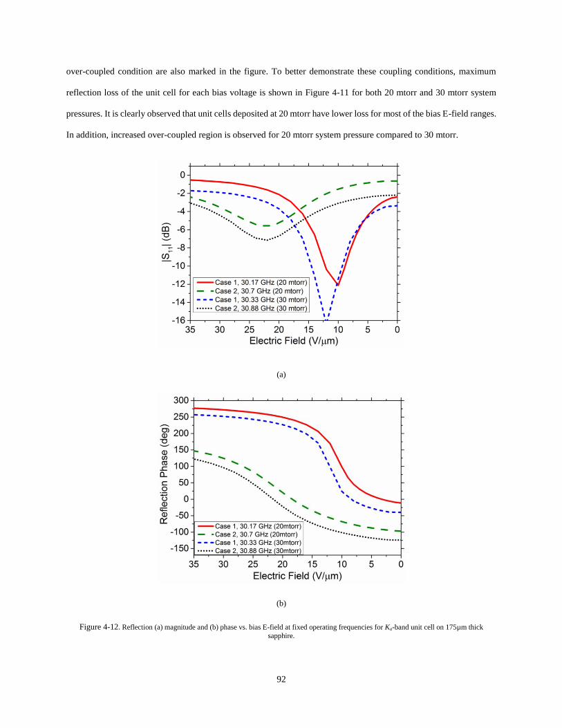
The measured reflection magnitudes for the two cases are shown in Figure. 2-28. When the inter-element spacing is
changed from chosen minimum to maximum values, the resonant frequency is shifted from 31.73 to 32.4 GHz. This
is equal to 2.1% variation with respect to the center frequency of 32 GHz, which agrees very well with the simulated
2.25% frequency shift. For the same variation in inter-element spacing, the reflection loss is increased by 2.4 dB
A = B = 0.45λ0 A = B = 0.75λ0
Sub-array
Ka-band waveguide
48
compared with 0.63 dB observed in simulations. This implies that not all the reflected energy is captured at the
waveguide port due to the non-broadside diffractions from the finite array. The measured reflection phases for the two
sub-arrays are plotted in Figure. 2-29. A phase difference (∆Phase) of 130o is observed at 32 GHz compared with
simulated 75o phase shift.
Figure. 2-28. Measured reflection magnitude in dB for minimum and maximum inter-element spacing.
Figure. 2-29. Measured reflection phase in degrees for minimum and maximum inter-element spacing.
28 30 32 34 36 38
-15
-10
-5
0
Frequency (GHz)
Norm
aili
zed S
11 (
dB
)
A=B=0.450
A=B=0.750
@fr = 31.7 GHz @f
r = 32.4 GHz
28 30 32 34 36 38-2000
-1500
-1000
-500
0
Frequency (GHz)
Refle
ctio
n P
hase
(deg)
A=B=0.450
A=B=0.750
@fr = 32.4 GHz
@fr = 31.7 GHz
fr
Phase
49
The measured results reveal the successful performance of the proposed setup in predicting the resonant frequency
behavior of reflectarray unit cells. Due to the approximate nature of the measurement setup and difficulties in phase
measurements in free-space, the measured and simulated ∆Phase are slightly off. Nevertheless, it is apparent that the
simplified finite sub-array approach can demonstrate the variations in reflection properties and provide valuable
insight to the underlying physics without the need of an infinite array.
50
CHAPTER 3: Q FACTOR ANALYSIS INVESTIGATING THE EFFECTS
FROM ANGLE OF INCIDENCE USING FLOQUET MODES
3.1. Introduction
A complete analytical approach to extract the reflection properties of unit cells using Q factors is discussed in the
previous chapter. The reasons for anomalous phase responses and the effects from the aforementioned physical
parameters on reflection properties were shown. However, the theory was developed for a single incident mode or
fixed incidence angle and therefore finds limited applications.
In this chapter, the Q factor analysis is extended and a theoretical model accounting for incidence angle and plane of
incidence are presented [77]. In general, the incident and reflected fields of a reflectarray are expressed in terms of
orthogonal Floquet modes. By expanding the coupled-mode theory, generic expressions for reflection coefficient of
multiple orthogonal modes are derived. The results, applied to reflectarrays, provide the reflection coefficients in terms
of the Q factors of the unit cell radiating into the Floquet modes. A rectangular patch antenna is chosen to illustrate
the concept, and closed-form expressions of the Q factors are derived in terms of the unit cell’s physical parameters
and angle of incidence. This allows the investigation of the reflection properties and coupling conditions of the
reflectarray without the need of full-wave simulations.
For demonstration, the effects of incidence angle for a single linearly-polarized (LP) incident wave are investigated
by choosing cases corresponding to different coupling conditions. The reasons for varied sensitivity of elements
located on different planes are explained. The presented theory expedites the design process of reflectarrays and
provides definitive physical perception.
3.2. Theoretical derivation
In this section, the reflection coefficients of reflectarray elements are presented in terms of Q factors. An arbitrary
incident plane wave with an oblique incidence angle can be expressed in terms of Floquet space harmonics [78]. The
analysis of an infinite array of identical elements shown in Figure. 3-1(a) is simplified into a single unit cell with
periodic boundaries as shown in Figure. 3-1(b). This model can be interpreted as an antenna element inside a
waveguide supporting Floquet modes. From a practical perspective where the grating lobes are undesired, dominant
Floquet modes TEz00 (transverse electric to z) and TMz00 (transverse magnetic to z) suffice in the analysis.
51
Figure. 3-1. (a) Reflectarray excited by a feed showing reference plane and angles of incidence. (b) Unit cell inside a waveguide
excited by Floquet modes. (c) Electric field and magnetic current distribution on the patch excited in (b) obtained from cavity
model.
The waveguide shown in Figure. 3-1(b) involves two orthogonally-polarized fundamental Floquet modes that are
coupled to the resonator; TE00 and TM00 of the waveguide coupled to TM010 mode of the patch. For an incidence angle
of 𝜃 in the Floquet waveguide analysis, where both the incident and reflected waves are expressed in terms of
fundamental Floquet modes, the angle of reflection is limited to – 𝜃. Due to the existence of two simultaneous modes
inside the waveguide, both co-coupling and cross-coupling of the modes occur. Co-coupling corresponds to the
coupling between the same modes, while cross-coupling corresponds to coupling between the orthogonal modes.
Under time-harmonic steady state condition, the co-coupled and cross-coupled reflection coefficients at the patch
surface are derived as follows using the coupled-mode theory:
Coupled-mode theory utilizing time reversibility and energy conservation are applied to derive the expressions for
reflection coefficients of multiple modes inside a waveguide. As shown in Figure. 3-1(b), if a resonating patch is
connected to a waveguide with two modes or two waveguides, the decay rate of the positive frequency mode amplitude
is given as [30]:
𝑑𝑎
𝑑𝑡= 𝑗𝜔0𝑎 − (
1
𝜏0
+1
𝜏𝑒1
+1
𝜏𝑒2
) 𝑎 + 𝑘1s+1 + 𝑘2s+2 (37)
(a) (b) (c)
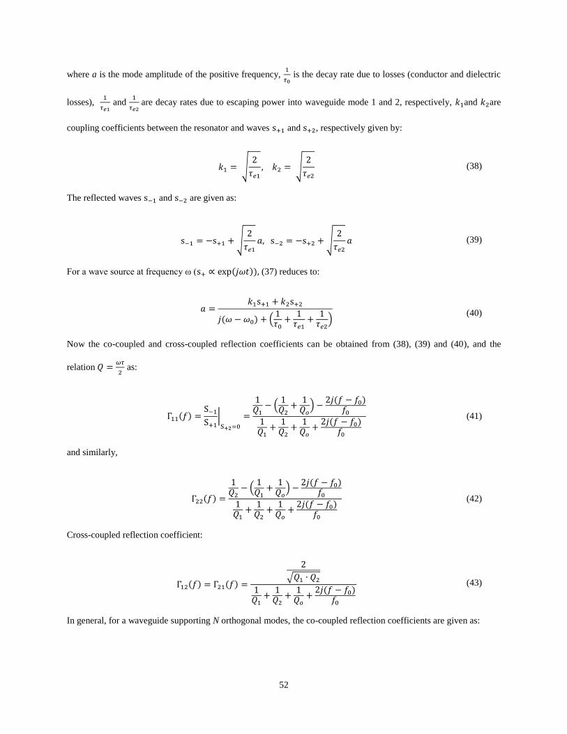
52
where a is the mode amplitude of the positive frequency, 1
𝜏0 is the decay rate due to losses (conductor and dielectric
losses), 1
𝜏𝑒1 and
1
𝜏𝑒2 are decay rates due to escaping power into waveguide mode 1 and 2, respectively, 𝑘1and 𝑘2are
coupling coefficients between the resonator and waves s+1 and s+2, respectively given by:
𝑘1 = √2
𝜏𝑒1
, 𝑘2 = √2
𝜏𝑒2
(38)
The reflected waves s−1 and s−2 are given as:
s−1 = −s+1 + √2
𝜏𝑒1
𝑎, s−2 = −s+2 + √2
𝜏𝑒2
𝑎 (39)
For a wave source at frequency ω (s+ ∝ exp(𝑗𝜔𝑡)), (37) reduces to:
𝑎 =𝑘1s+1 + 𝑘2s+2
𝑗(𝜔 − 𝜔0) + (1𝜏0
+1
𝜏𝑒1+
1𝜏𝑒2
)
(40)
Now the co-coupled and cross-coupled reflection coefficients can be obtained from (38), (39) and (40), and the
relation 𝑄 =𝜔𝜏
2 as:
Γ11(𝑓) =S−1
S+1
|S+2=0
=
1𝑄1
− (1
𝑄2+
1𝑄𝑜
) −2𝑗(𝑓 − 𝑓0)
𝑓0
1𝑄1
+1
𝑄2+
1𝑄𝑜
+2𝑗(𝑓 − 𝑓0)
𝑓0
(41)
and similarly,
Γ22(𝑓) =
1𝑄2
− (1
𝑄1+
1𝑄𝑜
) −2𝑗(𝑓 − 𝑓0)
𝑓0
1𝑄1
+1
𝑄2+
1𝑄𝑜
+2𝑗(𝑓 − 𝑓0)
𝑓0
(42)
Cross-coupled reflection coefficient:
Γ12(𝑓) = Γ21(𝑓) =
2
√𝑄1 ∙ 𝑄2
1𝑄1
+1
𝑄2+
1𝑄𝑜
+2𝑗(𝑓 − 𝑓0)
𝑓0
(43)
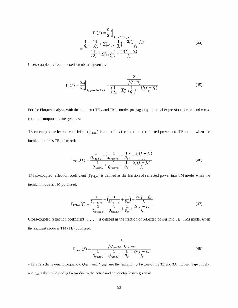
In general, for a waveguide supporting N orthogonal modes, the co-coupled reflection coefficients are given as:
53
Γii(𝑓) =S−i
S+i
|S+j=0 for 𝑗≠𝑖
=
1𝑄𝑖
− (1
𝑄𝑜+ ∑
1𝑄𝑗
𝑁𝑗=1,𝑗≠𝑖 ) −
2𝑗(𝑓 − 𝑓0)𝑓0
(1
𝑄𝑜+ ∑
1𝑄𝑗
𝑁𝑗=1 ) +
2𝑗(𝑓 − 𝑓0)𝑓0
(44)
Cross-coupled reflection coefficients are given as:
Γij(𝑓) =S−i
S+j
|S+k=0 for 𝑘≠𝑗
=
2
√𝑄𝑖 ∙ 𝑄𝑗
(1
𝑄𝑜+ ∑
1𝑄𝑗
𝑁𝑗=1 ) +
2𝑗(𝑓 − 𝑓0)𝑓0
(45)
For the Floquet analysis with the dominant TE00 and TM00 modes propagating, the final expressions for co- and cross-
coupled components are given as:
TE co-coupled reflection coefficient (ΓTEco) is defined as the fraction of reflected power into TE mode, when the
incident mode is TE polarized:
ΓTEco(𝑓) =
1𝑄𝑟𝑎𝑑𝑇𝐸
− (1
𝑄𝑟𝑎𝑑𝑇𝑀+
1𝑄𝑜
) −2𝑗(𝑓 − 𝑓0)
𝑓0
1𝑄𝑟𝑎𝑑𝑇𝐸
+1
𝑄𝑟𝑎𝑑𝑇𝑀+
1𝑄𝑜
+2𝑗(𝑓 − 𝑓0)
𝑓0
(46)
TM co-coupled reflection coefficient (ΓTMco) is defined as the fraction of reflected power into TM mode, when the
incident mode is TM polarized:
ΓTMco(𝑓) =
1𝑄𝑟𝑎𝑑𝑇𝑀
− (1
𝑄𝑟𝑎𝑑𝑇𝐸+
1𝑄𝑜
) −2𝑗(𝑓 − 𝑓0)
𝑓0
1𝑄𝑟𝑎𝑑𝑇𝐸
+1
𝑄𝑟𝑎𝑑𝑇𝑀+
1𝑄𝑜
+2𝑗(𝑓 − 𝑓0)
𝑓0
(47)
Cross-coupled reflection coefficient (Γcross) is defined as the fraction of reflected power into TE (TM) mode, when
the incident mode is TM (TE) polarized:
Γcross(𝑓) =
2
√𝑄𝑟𝑎𝑑𝑇𝐸 ∙ 𝑄𝑟𝑎𝑑𝑇𝑀
1𝑄𝑟𝑎𝑑𝑇𝐸
+1
𝑄𝑟𝑎𝑑𝑇𝑀+
1𝑄𝑜
+2𝑗(𝑓 − 𝑓0)
𝑓0
(48)
where f0 is the resonant frequency. QradTE and QradTM are the radiation Q factors of the TE and TM modes, respectively,
and Qo is the combined Q factor due to dielectric and conductor losses given as:
54
𝑄𝑐 = 𝑑√𝜋𝑓𝜇𝜎; 𝑄𝑑 =1
𝑡𝑎𝑛𝛿; 𝑄𝑜 =
𝑄𝑐𝑄𝑑
𝑄𝑐+𝑄𝑑
(49)
3.2.1. Derivation of QradTE and QradTM:
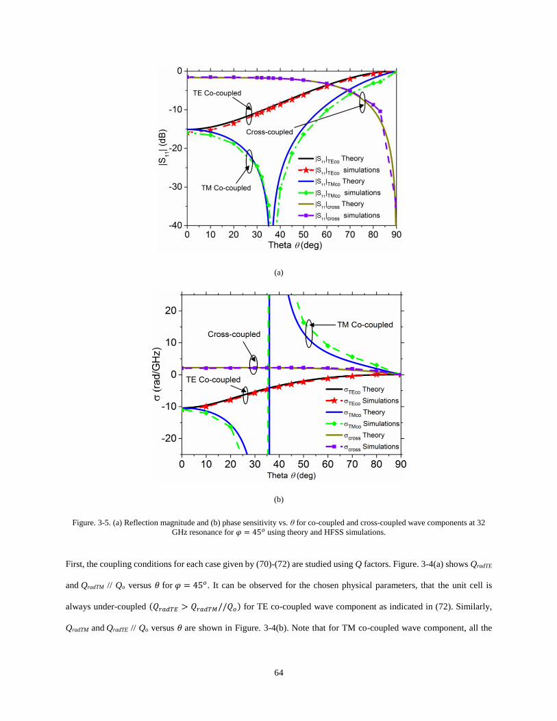
Floquet-mode and the cavity model of the patch antenna are utilized to derive the expressions for radiation Q factors
dependent on incidence angles (θ, 𝜑). In general, the radiation Q factor is given by:
𝑄𝑟𝑎𝑑 = 2𝜋𝑓0
𝐸𝑛𝑒𝑟𝑔𝑦 𝑠𝑡𝑜𝑟𝑒𝑑
𝑃𝑟𝑎𝑑
(50)
For all incidence angles, the dominant mode within the cavity is assumed to be TM010 mode as shown in the Figure.
3-1(c). Applying cavity model, image theory, and assuming a thin cavity, the patch antenna can be represented in
terms of equivalent magnetic currents at the radiating edges given as:
2,
2 , ˆ2 0
LLyxdEI m (51)
And at the non-radiating edges:
2/ , ˆsin2)( 0 WxyL
ydEyI m
(52)
If the field distribution is assumed to be confined underneath the patch, the stored electric energy is given by:
𝑊𝑒 =휀
4∬|𝐸|2𝑑𝑣 =
휀
8𝐸0
2𝑑𝑊𝐿 (53)
The modal transverse fields of TE and TM Floquet harmonics (with z-components suppressed) are given as [78]:
𝑇𝐸 =𝑘𝑦𝑚𝑛 − 𝑘𝑥𝑚𝑛
√𝑎𝑏(𝑘𝑥𝑚𝑛2 + 𝑘𝑦𝑚𝑛
2)
;
ℎ𝑇𝐸 =𝑘𝑥𝑚𝑛 + 𝑘𝑦𝑚𝑛
𝑍𝑇𝐸√𝑎𝑏(𝑘𝑥𝑚𝑛2 + 𝑘𝑦𝑚𝑛
2)
(54)
similarly,
𝑇𝑀 =𝑘𝑥𝑚𝑛 + 𝑘𝑦𝑚𝑛
√𝑎𝑏(𝑘𝑥𝑚𝑛2 + 𝑘𝑦𝑚𝑛
2)
;
ℎ𝑇𝑀 =−𝑘𝑦𝑚𝑛 + 𝑘𝑥𝑚𝑛
𝑍𝑇𝑀√𝑎𝑏(𝑘𝑥𝑚𝑛2 + 𝑘𝑦𝑚𝑛
2)
(55)
55
where a, b are the waveguide dimensions, ZTE and ZTM are the mode impedances of TE and TM modes, and 𝑘𝑥𝑚𝑛 ,
𝑘𝑦𝑚𝑛 are the wave numbers corresponding to (m, n) Floquet mode given by:
𝑘𝑥𝑚𝑛 = 𝑘0 sin 𝜃 cos 𝜑 +2𝑚𝜋
𝑎
𝑘𝑦𝑚𝑛 = 𝑘0 sin 𝜃 sin 𝜑 +2𝑛𝜋
𝑏
(56)
The amplitude A+ of TE and TM modes excited in the infinite waveguide by the volume magnetic current density can
be found using:
𝐴𝑇𝐸+ =
1
𝑃𝑇𝐸
∫ 𝐻𝑇𝐸 ∙ 𝑑𝑣 ;
𝐴𝑇𝑀+ =
1
𝑃𝑇𝑀
∫ 𝐻𝑇𝑀 ∙ 𝑑𝑣
(57)
where 𝐻𝑇𝐸, 𝑇𝑀 are the magnetic fields of the TE and TM modes and PTE, PTM are the normalization constants given
by:
𝑃𝑇𝐸 = 2 ∫ 𝑇𝐸 × ℎ𝑇𝐸 ∙ 𝑑𝑠 =2
𝑍𝑇𝐸
𝑃𝑇𝑀 = 2 ∫ 𝑇𝑀 × ℎ𝑇𝑀 ∙ 𝑑𝑠 =2
𝑍𝑇𝑀
(58)
Substituting equations (51), (52), (54), (56) in (57):
𝐴𝑇𝐸+ =
4𝑑𝐸0𝑊𝑘𝑥𝑚𝑛
𝑃𝑇𝐸𝑍𝑇𝐸√𝑎𝑏(𝑘𝑥𝑚𝑛2 + 𝑘𝑦𝑚𝑛
2)
(59)
similarly,
𝐴𝑇𝑀+ =
4𝑑𝐸0𝑊𝑘𝑦𝑚𝑛
𝑃𝑇𝑀𝑍𝑇𝑀√𝑎𝑏(𝑘𝑥𝑚𝑛2 + 𝑘𝑦𝑚𝑛
2)
(60)
The power carried by the TE and TM modes of the waveguide is:
𝑃𝑟𝑎𝑑𝑇𝐸 =1
2∫ 𝑇𝐸 × 𝐻∗
𝑇𝐸 ∙ 𝑑𝑠 =|𝐴𝑇𝐸
+|2
2𝑍𝑇𝐸
(61)
𝑃𝑟𝑎𝑑𝑇𝑀 =1
2∫ 𝑇𝑀 × 𝐻∗
𝑇𝑀 ∙ 𝑑𝑠 =|𝐴𝑇𝑀
+|2
2𝑍𝑇𝑀
(62)
The mode impedances of fundamental TE and TM modes, ZTE and ZTM are expressed in terms of free space wave
impedance (𝜂0) given by:
56
𝑍𝑇𝐸 =𝜂0
cos θ; 𝑍𝑇𝑀 = 𝜂0 ∙ cos θ (63)
At resonance, as the electric and magnetic energies are equal, QradTE and QradTM for the fundamental Floquet modes
(𝑚 = 𝑛 = 0) are derived as:
𝑄𝑟𝑎𝑑𝑇𝐸 =𝑓0𝜋휀
4𝑑
𝐿
𝑊𝑎𝑏
𝜂0
cos θ cos2 𝜑 (64)
and
𝑄𝑟𝑎𝑑𝑇𝑀 =𝑓0𝜋휀
4𝑑
𝐿
𝑊𝑎𝑏
𝜂0 cos θ
sin2 𝜑 (65)
Finally, the reflection coefficients of unit cell are determined by substituting the Q factors (49), (64) and (65) in (46),
(47) and (48). Using the developed theory, the reflection from a unit cell excited by a wave of any angle of incidence
and polarization can be analyzed.
For an arbitrary incident field on the array expressed in terms of Floquet harmonics (𝐸𝑖𝑛𝑐𝑇𝐸 , 𝐸𝑖𝑛𝑐
𝑇𝑀), the reflected TE
and TM components are given as:
[𝐸𝑟𝑒𝑓
𝑇𝐸
𝐸𝑟𝑒𝑓𝑇𝑀
] = [ΓTEco Γcross
Γcross ΓTMco
] [𝐸𝑖𝑛𝑐
𝑇𝐸
𝐸𝑖𝑛𝑐𝑇𝑀
] (66)
Even though, the total reflected fields are a combination as shown in (65), it is still beneficial to analyze each reflection
coefficient separately and illustrate the characteristics.
To comprehend the effects from angles of incidence and polarization, the antenna elements are assessed using two
important parameters for each wave component, reflection loss at resonance which determines the maximum loss, and
phase sensitivity (negative slope of the reflection phase at resonance) which determines the bandwidth, phase range
and sensitivity of the unit cells. Maximum reflection loss can be obtained from equations (46), (47) and (48). The
phase-sensitivity at f0 for co- and cross-coupled wave components is derived as:
For co-coupled wave components:
𝜎𝑇𝐸𝑐𝑜 =−𝜕∅𝑇𝐸𝑐𝑜
𝜕𝑓|
𝑓=𝑓0
≈4/𝑄𝑟𝑎𝑑𝑇𝐸
𝑓0 (1
𝑄𝑟𝑎𝑑𝑇𝐸2 − (
1𝑄𝑟𝑎𝑑𝑇𝑀
+1
𝑄𝑜)
2
)
(67)
similarly,
57
𝜎𝑇𝑀𝑐𝑜 =−𝜕∅𝑇𝑀𝑐𝑜
𝜕𝑓|
𝑓=𝑓0
≈4/𝑄𝑟𝑎𝑑𝑇𝑀
𝑓0 (1
𝑄𝑟𝑎𝑑𝑇𝑀2 − (
1𝑄𝑟𝑎𝑑𝑇𝐸
+1
𝑄𝑜)
2
)
(68)
And for cross-coupled wave components:
𝜎𝑐𝑟𝑜𝑠𝑠 =−𝜕∅𝑐𝑟𝑜𝑠𝑠
𝜕𝑓|
𝑓=𝑓0
≈
0 ( 𝑖𝑓 𝑄𝑟𝑎𝑑𝑇𝐸 = ∞ 𝑜𝑟 𝑄𝑟𝑎𝑑𝑇𝑀 = ∞ )2
𝑓0 (1
𝑄𝑟𝑎𝑑𝑇𝐸+
1𝑄𝑟𝑎𝑑𝑇𝑀
+1
𝑄𝑜)
(𝑒𝑙𝑠𝑒) (69)
where ∅𝑇𝐸𝑐𝑜 , ∅𝑇𝑀𝑐𝑜 , and ∅𝑐𝑟𝑜𝑠𝑠 are the reflection phases of ΓTEco, ΓTMco, and Γcross respectively.
3.3. Coupling conditions:
Depending on the relative values of Q factors, which are dependent on antenna physical parameters and incidence
angle, a unit cell can be over-coupled, critically-coupled, or under-coupled. Under TE excitation, an antenna element
is:
1. TE over-coupled, if
1
𝑄𝑟𝑎𝑑𝑇𝐸
>1
𝑄𝑟𝑎𝑑𝑇𝑀
+1
𝑄𝑜
; 𝜎𝑇𝐸𝑐𝑜 > 0 (70)
2. TE critically-coupled, if
1
𝑄𝑟𝑎𝑑𝑇𝐸
=1
𝑄𝑟𝑎𝑑𝑇𝑀
+1
𝑄𝑜
; 𝜎𝑇𝐸𝑐𝑜 = ∞ (71)
3. TE under-coupled, if
1
𝑄𝑟𝑎𝑑𝑇𝐸
<1
𝑄𝑟𝑎𝑑𝑇𝑀
+1
𝑄𝑜
; 𝜎𝑇𝐸𝑐𝑜 < 0 (72)
A special case of under-coupled occurs when 𝑄𝑟𝑎𝑑𝑇𝐸 = ∞, which corresponds to specular reflection or no
coupling,
𝑄𝑟𝑎𝑑𝑇𝐸 = ∞ ; 𝜎𝑇𝐸𝑐𝑜 = 0 (73)
similarly for TM excitation.
58
3.4. Analysis and validation
In this section, the effects of incidence angle on reflection properties are studied using the theory developed in section
2.2. for a single LP case. HFSS applying master-slave boundaries and Floquet port is used for simulation purposes.
A rectangular patch of dimensions 1.3×2 mm2 (L×W) on a 10-mil-thick RO3010 substrate (r = 10.2, tan = 0.0035,
½ oz copper) resonant at 32 GHz for normal incidence is used for demonstration. An inter-element spacing of 𝑎 =
𝑏 = 0.5𝜆0, where the higher-order Floquet modes are cutoff for all scan angles, is chosen.
For an array of reflectarray elements, there exists infinite sets of scan planes. However, the extremity in performance
is most likely to occur in cardinal (𝜑 = 90𝑜 , 𝜑 = 0𝑜) and inter-cardinal planes (φ = 45𝑜) [79]. Thus, elements
located on the principal planes or cardinal planes are chosen first. Later, the reflection properties of elements located
on inter-cardinal plane are also discussed.
3.4.1. H-plane (𝜑 = 0𝑜) & E-Plane (𝜑 = 90𝑜):
From Figure. 3-1(c), it can be observed that the polarization of the incident wave has to be y-polarized for the magnetic
currents on the radiating edges of the dominant mode to be along x. Thus for elements located on x-axis (𝜑 = 0𝑜),
which corresponds to H-plane, (64) and (65) reduce to:
𝑄𝑟𝑎𝑑𝑇𝐸 =𝑓0𝜋휀
4𝑑
𝐿
𝑊𝑎𝑏
𝜂0
cos θ (74)
and
𝑄𝑟𝑎𝑑𝑇𝑀 = ∞ (75)
Thus, equations (46), (47) and (48) reduce to:
ΓTEco(𝑓) =
1𝑄𝑟𝑎𝑑𝑇𝐸
−1
𝑄𝑜−
2𝑗(𝑓 − 𝑓0)𝑓0
1𝑄𝑟𝑎𝑑𝑇𝐸
+1
𝑄𝑜+
2𝑗(𝑓 − 𝑓0)𝑓0
(76)
ΓTMco(𝑓) = −1 (77)
Γcross(𝑓) = 0 (78)
The coupling conditions (70)-(72) reduce to:
59
1. Over-coupled, if Qo > QradTE.
2. Critically-coupled, if Qo = QradTE.
3. Under-coupled, if Qo < QradTE.
Similarly, for elements located on the principal E-plane (𝜑 = 90𝑜), (64), (65) reduces to:
𝑄𝑟𝑎𝑑𝑇𝐸 = ∞ (79)
and
𝑄𝑟𝑎𝑑𝑇𝑀 =𝑓0𝜋휀
4𝑑
𝐿
𝑊𝑎𝑏𝜂0 cos θ (80)
Reflection coefficients (46), (47) and (48) reduce to:
ΓTEco(𝑓) = −1 (81)
ΓTMco(𝑓) =
1𝑄𝑟𝑎𝑑𝑇𝑀
−1
𝑄𝑜−
2𝑗(𝑓 − 𝑓0)𝑓0
1𝑄𝑟𝑎𝑑𝑇𝑀
+1
𝑄𝑜+
2𝑗(𝑓 − 𝑓0)𝑓0
(82)
Γcross(𝑓) = 0 (83)
The coupling conditions reduce to:
1. Over-coupled, if Qo > QradTM.
2. Critically-coupled, if Qo = QradTM.
3. Under-coupled, if Qo < QradTM.
Note that cross-coupled reflection coefficients are zero for the elements on principal planes. Equations (77) and (81)
correspond to reflection coefficients from specular reflection. Thus, only ΓTEco(𝑓)and ΓTMco(𝑓) given by (76) and
(82) are the coefficients of interest for elements on H- and E-planes respectively.
60
(a)
(b)
Figure. 3-2. Q factors versus θ showing different coupling regions at 32 GHz for (a) 𝜑 = 0𝑜 and (b) 𝜑 = 90𝑜 using theory.
61
(a)
(b)
Figure. 3-3. (a) Reflection magnitude and (b) phase sensitivity vs. θ at resonance for 𝜑 = 0𝑜 and 𝜑 = 90𝑜 using theory and
HFSS simulations.
62
Q factors versus incidence angle 𝜃 for 𝜑 = 0𝑜 & 90𝑜are shown in Figure. 3-2(a) and Figure. 3-2(b) respectively. It is
observed that for 𝜑 = 0𝑜, critical coupling (Qo = QradTE) is observed at 𝜃 = 78𝑜. Unit cells are over-coupled (Qo >
QradTE) for 𝜃 < 78𝑜 and under-coupled (Qo < QradTE) for 𝜃 > 78𝑜. Reflectarray elements exhibit anomalous phase
response when under-coupled and cannot be used in any design [70]. Thus, the maximum incidence angle or scan
angle is limited by the critically-coupled condition of the antenna element. For 𝜑 = 90𝑜 as shown in Figure. 3-2(b),
Qo is greater than QradTM for all incidence angles, corresponding to over-coupled condition. On both planes for smaller
incidence angles (𝜃 < 40𝑜), the changes in radiation Q factors are small. However, for 𝜃 > 45𝑜, a noticeable change
in radiation Q factors w. r. t Qo is observed, particularly for elements on H-plane. This explains a similar behavior
observed in [80], where elements on the H-plane are found to be more sensitive to incidence angles than elements on
E-plane. These variations in Q factors render non-negligible effects on the reflection properties of unit cells which are
demonstrated in Figure. 3-3.
Maximum reflection loss and slope of the reflection phase at resonance versus 𝜃 for the two planes of incidence are
shown in Figure. 3-3(a) and Figure. 3-3(b), respectively. For 𝜑 = 0𝑜, it can be observed that as 𝜃 increases, reflection
loss and phase sensitivity (σTEco) remains almost constant for smaller incidence angles, and starts to increase drastically
for angles greater than 45𝑜. When the unit cell is critically coupled (𝜃 = 78𝑜), we note that maximum reflection loss
and singularity in σf are observed. For 𝜑 = 90𝑜 , it is observed that as 𝜃 increases reflection loss and σTMco decrease.
This decrease in σ, signifies the reduced sensitivity which implies increased bandwidth. It is noted that on 𝜑 = 90𝑜
plane, σTMco is positive for all the chosen 𝜃 implying over-coupled condition. For angles less than 40o, it is observed
that the variation in |S11| and σ versus 𝜃 for both the planes is small. A very good match between the full-wave
simulations and theoretical results is observed.
3.4.2. Inter-cardinal plane (𝜑 = 45𝑜)
To study the effects of incidence angles on elements off the principal planes, 𝜑 = 45𝑜 is chosen. Since the radiation
Q factors for both TE and TM modes are not infinite (except for grazing angles), both co-coupling and cross-coupling
conditions need to be addressed.
63
(a)
(b)
Figure. 3-4. Q factors vs. θ showing coupling regions for (a) TE co-coupled wave component and (b) TM co-coupled wave
component at 32 GHz resonance for 𝜑 = 45𝑜 using theory.
64
(a)
(b)
Figure. 3-5. (a) Reflection magnitude and (b) phase sensitivity vs. θ for co-coupled and cross-coupled wave components at 32
GHz resonance for 𝜑 = 45𝑜 using theory and HFSS simulations.
First, the coupling conditions for each case given by (70)-(72) are studied using Q factors. Figure. 3-4(a) shows QradTE
and QradTM // Qo versus 𝜃 for 𝜑 = 45𝑜. It can be observed for the chosen physical parameters, that the unit cell is
always under-coupled (𝑄𝑟𝑎𝑑𝑇𝐸 > 𝑄𝑟𝑎𝑑𝑇𝑀//𝑄𝑜) for TE co-coupled wave component as indicated in (72). Similarly,
QradTM and QradTE // Qo versus 𝜃 are shown in Figure. 3-4(b). Note that for TM co-coupled wave component, all the
65
three coupling-conditions exist. Critical-coupling is observed at 𝜃 = 36𝑜 . Under-coupled and over-coupled
conditions are also indicated.
To verify the loss performance, reflection magnitude for both co- and cross-coupled wave components are shown in
Figure. 3-5(a). For TE co-coupled wave component, even though loss decreases as 𝜃 increase, the unit cell exhibits
under-coupled condition. In the over-coupled region of the TM co-coupled wave component, loss is particularly high
for angles less than 50𝑜, and makes this region less useful as well. Thus, for 𝜑 = 45𝑜, the co-coupled reflection
coefficients suffer with anomalous phase responses or high loss for incidence angles less than 50𝑜 . In fact, the
significant contribution on this plane comes from the cross-coupling between the modes, where the unit cell is over-
coupled for all 𝜃, as shown in (69).
For cross-coupled wave component, reflection loss varies very slightly for angles less than 40𝑜 , and increases
drastically particularly for 𝜃 > 50𝑜 . It is also observed that at grazing angle 𝜃 = 90𝑜 , cross-coupled reflection
coefficient becomes zero.
Figure. 3-5(b) shows the variation of σ versus 𝜃 for both co- and cross-coupled wave components. It is observed that
σTEco is negative for all incidence angles, confirming the under-coupled condition. In the over-coupled region of TM
co-coupled wave component, σTMco decreases as 𝜃 increase. For the cross-coupled wave component, it is observed that
σcross is positive, varies slightly and tends toward zero. Again theoretical results closely follow simulation results.
3.4.3. Normal incidence (𝜃 = 𝜑 = 0𝑜)
The Q factors and reflection coefficient for unit cells excited by a normal incident plane wave are obtained by
substituting 𝜃 = 𝜑 = 0𝑜 in (64) and (65). Under normal incidence, cross-coupled reflection coefficient becomes zero
and the expression for radiation Q factor simplifies to:
𝑄𝑟𝑎𝑑𝑇𝐸𝑀 =𝑓0𝜋휀
4𝑑
𝐿
𝑊𝑎𝑏𝜂0 (84)
Reflection coefficient simplifies to:
Γ(𝑓) =
1𝑄𝑟𝑎𝑑𝑇𝐸𝑀
−1
𝑄𝑜−
2𝑗(𝑓 − 𝑓0)𝑓0
1𝑄𝑟𝑎𝑑𝑇𝐸𝑀
+1
𝑄𝑜+
2𝑗(𝑓 − 𝑓0)𝑓0
(85)
66
The expression for radiation Q factor obtained from Floquet modes is in agreement with the Q factor derived from
actual modal fields of normal incident plane wave reported in [81]. Equations (84) and (85) can be used for analyzing
the performance of reflectarray unit cells under normal incidence.
3.4.4. Combined effects of incidence angle and coupling conditions
In the previous sub-sections, the effects of incidence angle on a particular antenna element with fixed physical
parameters are shown. However, the sensitiveness to incidence angles and the reflection properties will vary with
coupling conditions, if any physical parameter is changed. In this sub-section, the effects of varying substrate
thicknesses on coupling regions are shown intuitively using graphical approach. In addition, the design curves showing
the coupling conditions for varying patch widths, dielectric constants and losses are also discussed.
First, the position of critical coupling and coupling regions for varying substrate thicknesses ranging from 1 mil (25.4
μm) to 20 mil (0.508 mm) are studied in Figure. 3-6. A resonance of 32 GHz is maintained by tailoring the patch
length, while the other dimensions are fixed (W = 2 mm, r = 10.2, tan = 0.0035, ½ oz copper). On H-plane, since
𝑄𝑟𝑎𝑑𝑇𝐸 is inversely proportional to 𝑐𝑜𝑠 𝜃, the under-coupled regions are observed for larger incidence angles as shown
in Figure. 3-6(a). Conversely on E-plane as shown in Figure. 3-6(b), the under-coupled regions are observed for
smaller incidence angles because 𝑄𝑟𝑎𝑑𝑇𝑀 is directly proportional to 𝑐𝑜𝑠 𝜃. On both the planes, it is also noted that as
the substrate thickness decreases, the available range of incidence angles for over-coupled condition decreases. It is
worth mentioning that even in the useful over-coupled region, the characteristics of the resonant patch element vary
with the Q factors.
67
(a)
(b)
Figure. 3-6. Demonstration of coupling regions of unit cells for varying substrate thicknesses and incidence angle θ on (a) 𝜑 =0𝑜 (H-plane) and (b) 𝜑 = 90𝑜 (E-plane).
To demonstrate this concept, two RO3010 substrates marked in Figure. 3-6 with thicknesses of 5 mil (0.127 mm), 20
mil (0.508 mm) corresponding to different levels of over-coupling under normal incidence (𝜃 = 𝜑 = 0𝑜) are chosen.
For reference, a center-fed circular reflectarray with a diameter of 15.5𝜆0 consisting of 749 elements and 𝑎 = 𝑏 =
0.5𝜆0 is chosen. A y-polarized ideal feed modeled as 𝑐𝑜𝑠𝑞𝜃, with q = 1.5 operating at 32 GHz is chosen as the feed
68
with f/D = 0.25. This setup corresponds to a maximum incidence angle of 63𝑜. The ideal phase shifts required on the
array surface to compensate for the differential spatial distances from the feed and achieve a broadside radiation pattern
are shown in Figure. 3-7(a).
To highlight the effects of incidence angle, the array elements over the aperture are designed to achieve the phases
shown in Figure. 3-7(a) using variable patch lengths and normal incidence (84), (85). Later, the Floquet theory
developed in the earlier section is utilized to extract the actual reflection coefficients on the antenna elements for the
incident polarization accounting for real incidence angles. The effects of incidence angle are first shown on reflection
phase, next on reflection magnitude and finally on the radiation patterns.
To comprehend the phase differences, the desired ideal phases are subtracted from the actual achieved phases and the
results are plotted. For d = 5 mil as shown in Figure. 3-7(b), considerable phase differences on the aperture are
observed. In particular, on 𝜑 = 0𝑜 plane, under-coupled condition is observed beyond 10th element from the array
center corresponding to an incidence angle of 53𝑜 which is in agreement with Figure. 3-6(a). Figure. 3-7(c)
corresponds to d = 20 mil, which is over-coupled for all the chosen range of incidence angles. However, noticeable
differences between the achieved and desired phase shifts are observed particularly for edge elements nearby principal
planes. A maximum phase variation of 43𝑜 is recorded over the array.
69
(a)
(b)
(c)
Figure. 3-7. (a) Ideal phase shifts required on each element, (b), (c) difference between the phase shifts obtained using Floquet
theory and (a), for d = 5, 20 mil and f/D = 0.25.
70
Similarly, the losses (in dB) for the chosen cases under normal incidence and accounting actual incidence angles are
plotted in Figure. 3-8. Figure. 3-8(a) and Figure. 3-8(b) correspond to losses under normal incidence for 5-mil- and
20-mil-thick substrates respectively. Similarly, Figure. 3-8(c) and Figure. 3-8(d) correspond to losses computed using
Floquet theory. It is observed that for both the cases, on the E-plane (𝜑 = 90𝑜), the losses computed using Floquet
theory are less than that of TEM theory. Conversely, on the H-plane (𝜑 = 0𝑜), the losses calculated considering actual
incidence angles are higher than normal incidence. In addition, very high losses are observed for thin 5-mil-substrate.
These variations in reflection magnitude and phase will affect the far-field performance of the antenna array.
(a)
(b)
5mil
20mil
71
(c)
(d)
Figure. 3-8. Reflection magnitude obtained for f/D = 0.25 by considering (a), (b) a fixed normal TEM incidence for d = 5 and 20
mil substrates. (c), (d) Floquet theory for d = 5 and 20 mil substrates.
5mil
20mil
72
(a)
(b)
Figure. 3-9. Radiation patterns on H- and E-planes for substrate thicknesses (a) 5 mil and (b) 20 mil using Floquet theory and
TEM.
Figure. 3-9 shows the radiation patterns on principal planes for both cases, computed using aperture fields from
Floquet theory and TEM normal incidence. From Figure. 3-9(a), for 5-mil case, even though considerable phase-
differences between the Floquet theory and TEM (Figure. 3-7(b)) are observed, due to very high losses (Figure. 3-8(a)
& Figure. 3-8(c)) the radiation patterns are closely matched. Conversely, for 20-mil case in Figure. 3-9(b), where the
73
phase differences are smaller than the 5-mil case, considerable differences in the side lobe levels of the radiation
pattern between Floquet and TEM theory are observed because of the low loss performance of the antenna elements.
The chosen scenario is a simple case study to demonstrate the effects of incidence angles using Q factors. The study
can be further extended to analyze other reflectarray configurations and antenna elements that are more sensitive to
incidence angles with high Q.
Lastly, the effects of other physical parameters, patch width (W), dielectric constant (r), loss tangent (tan ) and metal
conductivity (σ) in conjunction with incidence angle on coupling conditions are studied in Figure.3-10(a)-(h).
Figure.3-10(a) and Figure.3-10(b) show the coupling regions for varying patch widths and 𝜃 for a fixed substrate
RO3010 (r = 10.2, tan = 0.0035, ½ oz copper) of thickness 5 mil and 32 GHz resonance for H- and E- plane,
respectively. Figure.3-10(c) and Figure.3-10(d) correspond to varying dielectric constants at 32 GHz resonance, while
the other parameters are fixed (d = 5 mil, W = 2 mm, tan = 0.0035, ½ oz copper). Similarly, Figure.3-10(e)-(h)
correspond to varying loss tangents of the substrate (r = 10.2, d = 5 mil, W = 2 mm, ½ oz copper) and metal
conductivities (r = 10.2, d = 5 mil, W = 2 mm, tan = 0.0035) on both principal planes.
For all cases, it is confirmed that on H-plane the under-coupled conditions happen at larger incidence angles, and for
unit cells with small widths, and/or high dielectric and/or high loss substrates, and/or metals with low conductivities.
Few substrates and metals that could potentially lead into under-coupled condition for the chosen combination are
listed in Figure.3-10(e) and Figure.3-10(g). In addition, it is observed that on H-plane, the useful range of physical
parameters under consideration decrease as 𝜃 increase. Conversely on E-plane, the under-coupled condition occurs at
small incidence angles and the useful range increases as 𝜃 increase. Also observe that at 𝜃 = 0𝑜 for both planes, the
transition from under-coupled to over-coupled happens at the same point for all cases, such as W = 1.2 mm for varying
patch widths.
74
Figure.3-10. Demonstration of coupling regions of unit cells for varying patch widths, dielectric constants, substrate loss
tangents, metal conductivities vs. incidence angle θ on (a), (c), (e), (g) 𝜑 = 0𝑜 (H-plane) and (b), (d), (f), (h) 𝜑 = 90𝑜(E-plane).
(a) (b)
(d) (c)
(h)
(e)
(g)
(f)
75
3.4.5. Circuit model
In this section, a circuit model for the patch antenna excited by dominant Floquet TE and TM modes inside a
waveguide is presented as shown in Figure.3-11. First, the unloaded patch antenna is represented by a parallel RLC
circuit model whose parameters are given by:
𝐶𝑝 =휀0휀𝑟𝐿𝑊
2𝑑; 𝐿𝑝 =
1
𝜔02𝐶𝑝
; 𝑎𝑛𝑑 𝑅𝑖𝑛𝑡 =𝑄𝑜
𝜔0𝐶𝑝
(86)
Next, the coupling between the patch antenna and the Floquet modes are represented through transformers with ratios
n1 and n2, which can be expressed in terms of radiation quality factors as:
𝑄𝑟𝑎𝑑𝑇𝐸 = 𝜔0 ∙ 𝑛12 ∙
𝜂0
cos 𝜃∙ 𝐶𝑝 (87)
𝑄𝑟𝑎𝑑𝑇𝑀 = 𝜔0 ∙ 𝑛22 ∙ 𝜂0 cos 𝜃 ∙ 𝐶𝑝 (88)
By equating (64), (65), (87) and (88), the transformer ratios are derived as:
𝑛12 =
𝑎𝑏
4𝑊2 cos2 𝜑; 𝑛2
2 =𝑎𝑏
4𝑊2 sin2 𝜑 (89)
It can be observed that by using the quality factors, the circuit parameters are completely expressed in terms of physical
parameters of the patch, substrate properties and waveguide parameters.
Figure.3-11. Equivalent circuit model of a patch antenna excited by dominant Floquet modes inside a waveguide.
Similarly, the circuit model for TEM or TE10 excitation is shown in Figure 3-12, where
𝑛𝑇𝐸10 =𝜋
5.657∙ √
𝑏
𝑎∙
1
sin𝜋𝑊2𝑎
(90)
76
𝑛𝑇𝐸𝑀 =√𝑎𝑏
2𝑊 (36)
Figure 3-12. Equivalent circuit model of a patch antenna excited by a single incident wave (TE10 or TEM)
So far, the analysis is carried out for a rectangular patch elements using Q factors and coupling conditions. In the next
chapter, the analysis of a tunable reflectarray element required to realize a beam-steerable reflectarray antenna is
presented and the performance is optimized utilizing the coupling conditions.
77
CHAPTER 4: REFLECTARRAY BASED ON BST INTEGRATED
CAPACITIVELY LOADED PATCH
4.1. Introduction
To realize a beam-steerable reflectarray antenna, the phase of each antenna element has to be controllable. In this
chapter, first the integration of BST with the reflectarray element is discussed. Next, the biasing schemes for the
normal operation of the antenna elements are discussed. Finally, a reflectarray prototype capable of electrically
scanning the beam is presented. The Unit cell design chosen in this design is similar to [60] and its performance is
improved considerably by optimizing the BST deposition and biasing scheme. Utilizing the coupling regions
introduced in [70], a detailed analysis on the effects of coupling conditions on the tunable unit cell’s performance is
also shown.
A 400 nm thick BST thin-film grown by RF magnetron sputtering is used as the tuning mechanism compared to 5 μm
thick film in [60]. This enables the possibility of the unit cell being transferred to a flexible substrate [82]. The designed
BST-integrated X and Ka band reflectarray elements are fabricated using micro-fabrication techniques and measured
via waveguide approach. To author’s knowledge, this report showcases a continuously tunable BST-integrated
reflectarray antenna at Ka band for the first time, and an X-band unit cell with enhanced performance.
4.2. Analysis using full-wave simulations
The reconfigurable reflectarray element chosen in this study is based on a complex oxide BST thin-film varactor. Ba1-
x SrxTiO3 is the solid solution of barium titanate and strontium titanate. By applying a variable DC voltage across the
electrodes of the BST capacitor, the dielectric constant is varied and a tunable capacitor is realized.
A schematic of the reflectarray using the proposed unit cell is shown in Figure 4-1(a).The reconfigurable reflectarray
element consists of two quarter-wavelength-long patches coupled through the Ba0.5Sr0.5TiO3 capacitor as shown in
Figure 4-1(b). The antenna elements are designed to operate at X and Ka bands in view of space applications. Fixed
gap dimensions of 20 μm for X band and 10 μm for Ka band between the patch elements are chosen, respectively. The
width of the BST layer is slightly greater than the gap dimension to allow overlap between the patch and BST in order
to form reliable electrical connection. Rectangular metallic waveguide excitation shown in Figure 4-1(c), with the
dominant TE10 mode propagating is used for the extraction of reflection properties.
78
(a)
(b) (c)
Figure 4-1. (a) A schematics of a 7×7 reflectarray using the proposed antenna elements including the feed, (b) proposed BST-integrated
reflectarray element, and (c) rectangular metallic waveguide used to characterize the element shown in (b).
The dielectric constant and loss tangent of BST are functions of applied voltage and frequency. The varying DC
voltages are simulated by tuning the relative dielectric constant and loss tangent of the BST. This facilitates the study
of coupling conditions and the effects of BST film properties. In general, higher permittivity and loss are observed for
lower DC voltage and vice-versa. For the analysis, dielectric properties of the BST are extracted from the unit cell
Feed horn
Unit cell loaded
with BST
7 × 7 reflectarray
BST layer
under the gap
substrate
patch
BSTgap
ground plane
substrate
patch
gap
ground plane
lumped C
79
measurements which are presented in the later section of the report. A relative dielectric constant swept from 500 to
250 for the Ka-band and 600 to 300 for the X-band unit cells are used in the simulations.
BST being a high permittivity material, usually in the ranges of hundred, when integrated with an antenna element
will affect the Q factors and the coupling conditions. In addition, the substrate properties are also shown to
significantly affect the performance of a reflectarray. As shown in [70], under-coupled unit cells exhibit anomalous
phase responses. Unit cells close to critically-coupled condition suffer with very high losses but provide maximum
phase sensitivity and phase range. On the other hand, over-coupled unit cells usually have reasonable losses but with
limited phase range. In this paper, sapphire (r = 10) is chosen as the substrate for its favorable properties of BST
growth and very low loss [83]. A detailed analysis on the effects of substrate thickness on coupling conditions and
unit cell performance is shown in the following subsection.
In the first step, two extreme cases of r = 500, tan = 0.16 and r = 250, tan = 0.04 corresponding to lowest and
highest applied electric field at Ka band are chosen for the BST. Substrate thicknesses ranging from 50 to 500 μm are
used. For simplicity, dielectric constant and loss of the BST are assumed to be constant w. r. t frequency and substrate
thickness. The width of the antenna element is fixed at 2.3 mm and 800-nm-thick copper is used for the metal layer.
For each substrate thickness, the unit cell is designed to resonate at a fixed frequency of 29 GHz for a BST r = 500
by tailoring the resonant dimension from 2.75 mm (h = 50 μm) to 1.42 mm (h = 500 μm).
Reflection loss at resonance (Min(|S11|)), which corresponds to the maximum loss of the unit cell, and phase sensitivity
(σf) defined as negative of the slope of the reflection phase at resonance, are used to study the coupling regions and
evaluate the performance of the antenna element. Throughout the paper, Min(|S11|) is used to study the coupling
conditions. Whereas |S11| is used to quantify the loss of the unit cell at a fixed frequency, which in general is the center
frequency of the array.
80
(a)
(b)
Figure 4-2. (a) Reflection magnitude and (b) phase sensitivity vs. substrate thickness at resonant frequency of the unit cells showing the
coupling regions.
Figure 4-2 (a) shows the maximum reflection loss versus substrate thickness for the two chosen permittivities at their
respective resonant frequencies. It is observed that for the higher dielectric constant case (r = 500, tan = 0.16), all
the three coupling regions; under-coupled, critically-coupled and over-coupled are observed. However, for lower
81
dielectric constant case (r = 250, tan = 0.04), the patch elements are over-coupled for the entire range of substrate
thicknesses. Therefore, a unit cell corresponding to a substrate thickness in the under-coupled region can become over-
coupled for higher bias voltages. Thus, under-coupled unit cells are not completely undesirable for the presented
antenna element. It is important to note that for a passive reflectarray element, a unit cell in the under-coupled region
is not useful because its Q factors will not change considerably by adjusting its resonant dimension. In the under-
coupled region of the high dielectric constant case, reflection loss increases as the substrate thickness increases.
Maximum loss is observed at the critically-coupled condition. As expected, in the over-coupled region for both cases,
the reflection loss decreases as the substrate thickness increases.
Phase sensitivity (σf) versus substrate thickness is shown in Figure 4-2(b). For the high dielectric constant case, it is
observed that the phase sensitivity, which determines the bandwidth and phase range, is higher around the critically-
coupled region. Antenna elements operating at this region will provide maximum phase range at the expense of
additional losses. As the substrate thickness increases in the over-coupled region, phase sensitivity decreases, which
implies increased bandwidth and reduced phase range. On the other hand, for the low dielectric constant case, all the
antenna elements are over-coupled and phase sensitivity decreases as substrate thickness increases.
82
(a)
(b)
Figure 4-3.(a) Reflection magnitude and (b) phase sensitivity vs. dielectric constant at the resonant frequency of the unit cells showing the
coupling regions for three substrate thicknesses
To achieve an optimal performance in terms of loss and phase range, unit cells on three substrate thicknesses h = 175,
300, 450 μm, corresponding to different levels of coupling conditions are studied. Again for each substrate thickness,
the unit cell is designed to resonate at 29 GHz for a BST permittivity of r = 500. The resonant dimension are found
to be 2 mm, 1.75 mm and 1.5 mm for h = 175, 300, 450 μm respectively. To demonstrate the tunability of the antenna
83
element, BST permittivity is varied from 500 to 250 in steps of 25. The loss tangent of the BST film is swept from
0.16 to 0.04 in steps of 0.012, where high loss tangent (0.16) corresponds to high BST permittivity (r = 500) and
vice-versa. For the chosen range of relative dielectric constants, a frequency tunability of 7.4%, 5.7% and 4% are
observed for 175, 300 and 450 μm respectively.
Figure 4-3(a) shows the maximum reflection loss observed for each dielectric constant. It is observed that the unit
cells designed on 175 μm substrate undergo all the three coupling conditions. As pointed out earlier, even though 175
μm case is under-coupled for high BST permittivities (low DC voltage), as the applied voltage increases its permittivity
decreases and the antenna becomes over-coupled. On the other hand, relatively thicker substrates 300 and 450 μm are
always over-coupled. As expected, thicker substrates exhibit lower losses. However, thicker substrates possess smaller
phase sensitivity (σf) implying lower phase range as shown in Figure 4-3(b).
To quantify these effects, design curves showing permittivity versus reflection magnitude and phase, at fixed operating
frequencies are shown in Figure 4-4. For 175-μm-thick substrate, the curves are plotted at two different frequencies
of 30.34 GHz and 30.8 GHz, corresponding to maximum phase range of 277o and a phase range of 250o respectively.
For the maximum phase range case, the losses are extremely high as seen in Figure 4-4(b). Hence, a different frequency
of 30.8 GHz is picked, where losses are considerably reduced by limiting the phase range to 250o. For 300 μm and
450 μm thick substrates, curves are shown at their respective frequencies corresponding to maximum phase range.
Unit cells designed on 300 μm substrates have slightly better loss performance, but the overall phase range is observed
to be less than 200o. Similarly, unit cells on 450 μm substrate exhibit considerably-lower losses, however suffer from
a very low phase range of 102o. Therefore, 175-μm-thick substrate operating near the critically-coupled region is
chosen for the measurement purposes at Ka band. A similar analysis is performed at X band, and a substrate thickness
of 430 μm which is over-coupled and operates close to the critically-coupled condition is used.
84
(a)
(b)
Figure 4-4 .Reflection (a) phase and (b) magnitude at a fixed operating frequency showing the phase range and loss performance of the unit
cells.
In order to apply DC bias voltages to the BST thin film, and at the same time have the least effect on the total
performance, special design is needed for DC bias lines. Three different configurations for biasing lines as shown in
Figure 4-5 are discussed. Figure 4-5(a) corresponds to the antenna element without any bias lines; Figure 4-5(b),
Figure 4-5(c) and Figure 4-5(d) correspond to the configurations where bias lines are connected to the edge, middle
85
and minimum E-field point on each patch, respectively. Moreover, high-impedance lines are defined by using highly-
resistive chromium for X-band unit cell. For the sake of brevity, the simulations are performed for a fixed permittivity
(r = 300) and loss tangent (tan = 0.105) at X band. A square patch of 6.56.5 mm2 on a 430-μm-thick sapphire
substrate operating at X band is chosen. For Ka band, another biasing scheme based on radial stubs is presented.
Figure 4-5. Different bias line configurations. (a) No bias lines, (b) horizontal bias lines at the corner of each patch, (c) horizontal bias lines at
the middle of each patch, and (d) horizontal bias lines at the Emin of the patch (1.26mm from the center of the unit cell).
Figure 4-6. Current density for different bias lines. (a) No bias lines, (b) horizontal bias lines at the corner of each patch, (c) horizontal bias lines
at the middle of each patch, and (d) horizontal bias lines at the Emin of the patch.
To evaluate the biasing schemes, the surface current density at resonance for each case is plotted in Figure 4-6. The
corresponding reflection magnitude and phase are shown in Figure 4-7. It is obvious that Case (d) with horizontal bias
No
Bias
Lines
Best
Design
(a) (b)
(c) (d)
(a) (b)
(c) (d)
86
lines connected to the minimum E-field point on the patch share the most similarity of current density distribution as
Case (a) without bias lines. However, biasing schemes (b) and (c) disturb the mode of the patch as observed from the
current densities and result in undesired responses as shown in Figure 4-7(a) and Figure 4-7(b). It is also noted that
when the biasing lines are connected to the edge of the patch, where the E-field is maximum, the affects from the
biasing are dominant. Thus, the horizontal bias lines connected to the minimum E-field point is the best choice as
confirmed from Figure 4-7(a) & Figure 4-7(b).
For Ka-band unit cell, the presence of biasing pads inside the waveguide is not practical due to the waveguide
dimension limitations. Keeping this in mind, an optimized biasing scheme based on the radial stub is proposed. In the
first step of bias line optimization, the biasing lines are connected to the minimum E-field points on each quarter-
wavelength-long patches. Additionally, a half-wave length radial stub is used to provide a very high impedance (open-
circuit) looking from the patch. Then, the vertical biasing lines start from the short-circuit point of the radial stub and
run all the way towards the waveguide edge, which can be connected to soldering pads during measurements, as shown
in Figure 4-8(a). For measurement purposes, a customized waveguide setup as shown in Figure 4-8(a) is designed. It
is important to note that an intermediate waveguide holder with grooves aligned to the bias-lines is fabricated to avoid
short circuit between the patch element and Ka-band waveguide adaptor. The comparison between the reflection
properties of the Ka-band unit cell with and without the radial stub biasing scheme is shown in the measurement
section.
87
(a)
(b)
Figure 4-7. A reflectarray unit cell loaded with a BST layer acting as a distributed capacitance and corresponding reflection (a) magnitude and
(b) phase for different biasing schemes.
88
(a)
(b)
89
(c)
(d)
Figure 4-8. (a) Ka-band measurement setup showing the fabricated reflectarray element with the biasing lines, sample holder and the waveguide
adaptor, (b) fabrication steps for the proposed unit cells, (c) Top view of an X-band BST-based reflectarray unit cell, and (d) measurement setup
at X band with the sample holder.
4.3. Unit cell fabrications and measurements
In this section, the proposed BST-loaded reflectarray unit cell fabrication is discussed following the steps shown in
Figure 4-8(b). Next, the measurement results for different cases are shown. The Sapphire wafer is cut to the same size
as the cross section of X- and Ka-band sample holders using MTI Precision CNC Dicing/Cutting Saw (SYJ-400). Then,
a BST thin-film layer of 400 nm thick is deposited using RF sputtering system (AJA ATC 1800). Two targets from
different vendors are used for X- and Ka-band designs. A system pressure (Psys) of 5 mtorr is used for the X-band unit
BST
Patch
Soldering PadBias Line
X-band
Waveguide
Flange with
RA Unit Cell
90
cell fabrication on a 430 μm thick sapphire substrate. For the Ka-band unit cell fabrications, two system pressures of
20 mtorr and 30 mtorr are used.
Figure 4-9. Measured reflection magnitude and phase of the unit cells with and without the biasing lines at Ka band.
After deposition, the BST layer is etched in diluted HF solution to a size that is slightly larger than the gap in both
horizontal and vertical directions. A 2% solution of commercially-available HF is used for etching. Next the sample
is annealed at 900o for 20 hours (X band) / 12 hours (Ka band) in a box oven with an oxygen flow under atmosphere
pressure. For X-band unit cell, Cr bias lines of 20 μm wide and 300 nm thick are then deposited and patterned using
liftoff. The resistance of each bias line is about 3 kΩ (measured using a digital multi-meter). After that, 1.3-µm-thick
copper patch and soldering pads are deposited in the same run using an E-beam evaporator and patterned using liftoff.
For the Ka-band unit cell, patterns for both patch and bias lines are defined using a single layer mask. A 750-nm-thick
copper layer is deposited using E-beam evaporation and patterned using lift-off. A 50-nm-thick chromium layer is
thermally evaporated to promote the adhesion between copper and substrate. Finally, 1.3-µm-thick copper is deposited
on the back side of the substrate to form the ground plane.
The fabricated BST-loaded reflectarray unit cells and the measurement setup are illustrated in Figure 4-8. The
measured results at Ka band obtained for the BST-loaded patch element with and without the bias lines on a 175-μm-
91
thick substrate at 20 mtorr system pressure are shown in Figure 4-9. It is clearly observed that the effects from biasing
line are minimal.
Figure 4-10. Measured reflection magnitude vs. frequency for varying bias E-field.
Figure 4-11. Reflection magnitude vs. bias E-field showing the coupling conditions for two system pressures.
Figure 4-10 shows the resonant frequency variation of the Ka-band unit cell with the applied bias E-field for 20 mtorr
system pressure. A resonant frequency shift from 29.22 GHz to 30.93 GHz corresponding to 5.8% change in resonant
frequency is observed for an applied E-field variation of 0-35 V/μm. As expected, it is also observed that the unit cells
are under-coupled for the applied E-fields lower than 1.3 V/μm. Unit cells corresponding to critically-coupled and
Case 1 Case 2
92
over-coupled condition are also marked in the figure. To better demonstrate these coupling conditions, maximum
reflection loss of the unit cell for each bias voltage is shown in Figure 4-11 for both 20 mtorr and 30 mtorr system
pressures. It is clearly observed that unit cells deposited at 20 mtorr have lower loss for most of the bias E-field ranges.
In addition, increased over-coupled region is observed for 20 mtorr system pressure compared to 30 mtorr.
(a)
(b)
Figure 4-12. Reflection (a) magnitude and (b) phase vs. bias E-field at fixed operating frequencies for Ka-band unit cell on 175µm thick
sapphire.
93
(a)
(b)
Figure 4-13. Reflection (a) magnitude and (b) phase vs. bias E-field at fixed operating frequencies for Ka-band unit cell on 250µm thick
sapphire.
94
To evaluate the performance of the unit cells, design curves showing reflection magnitude and phase range for two
cases are shown in Figure 4-12. While presenting the reflection magnitude, additional losses from the sample holder
are subtracted from the measured data. Case 1 corresponds to the frequency, where maximum phase range for the
over-coupled unit cells is observed. Case 2 corresponds to the frequency where a phase range of 250o is recorded.
Frequencies corresponding to Case 1 for 20 mtorr and 30 mtorr system pressures are found to be 30.17 GHz and 30.33
GHz, respectively. Similarly for Case 2, the graphs are plotted at 30.7 GHz and 30.88 GHz for 20 mtorr and 30 mtorr
pressures, respectively. It is clearly observed from Figure 4-12(a) and Figure 4-12(b) that the reflection loss is very
high for Case 1, even though a phase range close to 300o is observed for both system pressures. Specifically, a phase
range of 283o and 298o are observed for 20 mtorr and 30 mtorr system pressures. On the other hand, if the unit cells
are operated at frequencies corresponding to a phase range of 250o (Case 2), losses are significantly reduced for both
system pressures. A maximum reflection loss of 5.6 dB and 7.1 dB are observed for 20 mtorr and 30 mtorr pressures,
respectively. Comparing the losses between the two system pressures, unit cells fabricated at 20 mtorr have on average
approximately 1-dB less loss than those at 30 mtorr for a phase range of 250o. Thus lowering the system pressure will
improve the loss performance. However, it is important to note that the tunability of the BST thin-film decreases if
the system pressure during deposition is reduced. A compromise between the phase range and reflection loss is
required for the optimal performance. Similarly, another unit cell operating at Ka band on a 250µm sapphire at 20mtorr
system pressure is fabricated and the results are plotted in Figure 4-13.A maximum phase range of 222o with a
maximum reflection loss of 7.5 dB at 30.16 GHz is measured.
Now design curves for the X-band unit cell on 430-μm-thick substrate are shown in Figure 4-14. An electric field
variation of 0-20 V/μm is used in the measurements. Case 1 corresponds to maximum phase range while Case 2
corresponds to a phase range of 250o. It is observed that when the unit cells are operating at the frequency
corresponding to maximum phase range (10.15 GHz), a maximum reflection loss of 8.9 dB and phase range of 263o
are observed. In Case 2 (10.27 GHz), the maximum reflection loss is reduced to 5.8 dB.
95
(a)
(b)
Figure 4-14. Reflection (a) magnitude and (b) phase vs. bias E-field at fixed operating frequencies for X-band unit cell.
4.4. BST properties and unit cell analysis
In this subsection, the design of a 45-element Ka-band reflectarray prototype based on the unit cell presented in the
earlier section is described. Earlier, the effects of system pressure, operating frequency and substrate thickness on the
unit cell performance were shown. It is important to note that the S-curves presented in Figure 4-12 were based on
96
rectangular metallic waveguide simulations with an inter element spacing of 7.112 mm and 3.556 mm. However, for
an array design, it is common to extract the S-curves from TEM waveguide with an inter-element spacing equal to the
actual spacing between the elements in the final array. Hence the dielectric properties of the BST thin film for different
bias E-field are estimated from the measured data for a system pressure of 20 mtorr and plotted in Figure 4-15. This
enables the study of the reflection properties of the unit cell for any case of interest using full-wave simulations. From
Figure 4-15, it is observed that the dielectric constant varies from 500 to 275, while loss tangent varies from 0.12 to
0.03 for an E-field variation of 0 – 35 V/um.
Figure 4-15. Estimated BST properties extracted from measurements at Ka band.
4.4.1. TEM Analysis
First, the analysis of unit cell is performed using a parallel-plate TEM waveguide in High Frequency Structure
Simulator (HFSS). An operating frequency of 31.6 GHz and a fixed inter-element spacing of a = b = 4 mm is chosen.
The dimensions of the patch element are 2.3 mm (W) and 1.9 mm (L) with a fixed gap size of 10 μm. The dimensions
of BST are slightly larger than the gap size to ensure a reliable electrical connection between the patch elements and
the BST thin film.
The analysis is carried out by varying the BST dielectric constant from 275 to 500 in steps of 25, and loss tangent
from 0.03 to 0.12 in steps of 0.01. The resulting S-curves showing the variation of reflection magnitude and phase
97
versus BST permittivity are shown in the Figure 4-16. It is important to note that the frequency of operation is
picked to achieve an overall phase range close to 240o. From Figure 4-16(a) it is observed that the reflection loss
varies from 1 dB to 7.5 dB for the chosen range of dielectric properties of BST. Maximum reflection loss is
observed for a BST relative permittivity of 375. An overall phase variation of approximately 240o is observed as
shown in Figure 4-16(b).
(a)
(b)
Figure 4-16. Reflection (a) magnitude, and (b) phase vs. BST dielectric constant at 31.6 GHz for normal TEM incidence
98
4.4.2. Floquet Analysis
To understand the effects from incidence angles on the reflection properties of the antenna elements, Floquet analysis
is used. HFSS simulations employing master-slave boundaries are used to extract the S-curves. Incidence angles up
to 40o for both TE and TM polarizations are simulated and compared with the normal incidence. From Figure 4-17, it
is observed that the reflection losses of the unit cells excited by TE waves (elements on the H-plane) are higher than
the normal incidence. It is also observed that on H-plane, the reflection loss increases as incidence angles increases as
explained in the previous chapter. On the other, for the elements on the E-plane (TM), reflection loss is smaller than
the normal incidence case, and decreases as the incidence angle increase. The variation of reflection phase versus BST
dielectric constant for different incidence angles and polarization are shown in Figure 4-18. It is seen that the overall
phase range decreases very slightly for the elements located on the E-plane (TM) compared to the normal incidence.
On the other hand for the elements on the H-plane (TE), the overall phase range increases with the incidence angles.
This behavior is due to increase in the phase-sensitivity. Overall, the effects from varying incidence angle are smaller
for incidence angles up to 30o and start to increase for higher incidence angles particularly on H-plane.
Figure 4-17. S-curves showing reflection magnitude for varying incident angles using Floquet analysis.
99
Figure 4-18. S-curves showing reflection phase for varying incident angles using Floquet analysis.
4.5. Array analysis using full-wave simulations
In this section, first the biasing schemes for the unit cell described in the previous section are discussed. Later, a
reflectarray prototype is analyzed using full-wave simulations. A simplified phase assignment to reduce the number
of voltage sources for E-plane scanning is also discussed. Finally, the beam-scanning capability of the array is
demonstrated on H- plane using individual phase control.
4.5.1. Biasing schemes
Ideally, every element in the array will have an individual phase control to achieve beam scanning. However, such a
demonstration is particularly expensive since it requires a power supply for every single antenna element. For this
purpose, two simplified biasing schemes shown in Figure 4-19 are studied. Type-1 and type-2 correspond to the cases
where the antenna elements are connected along the E-plane, and H-plane, respectively. By using such a simplified
biasing scheme, every antenna along each row or column can be controlled by a single power supply and beam
scanning along a single plane can be demonstrated. This simplified biasing scheme helps to demonstrate the beam-
scanning capability of the array with reasonable costs.
The bias lines are defined using high impedance chromium lines connected to the minimum E-field point on each
quarter wavelength patch. The study is carried out for a fixed normal incidence and polarization with E-field along y-
axis. The comparison between the S-curves with and without the biasing lines is shown in Figure 4-20. It is clearly
100
observed, for type-2, where the elements are connected along H-plane the affects from biasing are minimal. On the
other hand, for type-2 biasing scheme, significantly higher losses with completely different phase response is
observed. Hence, type-2 biasing scheme is chosen for the array design.
Figure 4-19. Two types of biasing schemes considered to minimize their affects.
Figure 4-20. S-curves for different biasing schemes using full-wave simulations
101
4.5.2. Array analysis using full-wave simulations
For the demonstration, a 5×9 (45) element array with an offset feed configuration of θf = 25o along y-axis is chosen.
A Ka-band horn antenna with the beam pointing towards the center of the array is applied. For biasing, type-2 biasing
scheme where the elements along H-plane are controlled by a single voltage is used. By choosing a large f/D and
placing the feed along E-plane (y-axis), similar phase-delays for the elements along each column can be achieved and
beam-scanning along E-plane can be demonstrated. For this reason, a large f/D = 1.95 is chosen. This corresponds to
an aperture efficiency of ~27% and an incidence angle of 36o. For the analysis and design of the array, the unit cell
simulations based on TEM waveguide are used. HFSS using Finite Element Boundary Integral (FEBI) boundary
conditions is used to analyze the array performance. By using FEBI, the radiation boundary can be defined just around
the feed and the array. The structures inside the FEBI are analyzed using FEM and the interactions between the
structures are analyzed using boundary integral equations, which significantly reduces the simulation complexity
compared to a standard radiation boundary.
In addition, due to the small size of the gap (10 μm) and high dielectric constants of BST it is computationally very
expensive to perform the full-wave simulations. To simplify the simulation complexity, BST material is approximated
by the HFSS lumped element model. The varying BST permittivity and loss tangent are simulated by changing the
capacitance and resistance values of the parallel RC lumped elements. For the chosen BST dielectric property
variations, capacitance ranging from 0.42 – 0.23 pF and resistance from 105 – 720 ohms are obtained.
For the array analysis, first the lumped element parameters of the BST are chosen to achieve the phase distributions
required to scan the beam along E-plane. The elements along each column are assigned the same lumped element
parameters to replicate the simplified biasing scheme as shown in Figure 4-21.
102
Figure 4-21. A schematic of a 5×9 reflectarray using the BST-integrated capacitively loaded patches.
Figure 4-22(a) shows the normalized radiation patterns for E-plane scan up to 25o. Only the scan cases along the image
side of the feed are shown due to the feed blockage. In Figure 4-22(b), the E- and H-plane patterns for the broad-side
case are shown. From Figure 4-22, it is observed that the narrow main lobes are observed for the E-plane patterns
compared to H-plane patterns as expected due to the larger size along E-plane. Higher side lobe levels are observed
for the E-plane radiation patterns, particularly for the broad-side case due to the simplified biasing scheme and also
the scan angle being close to the feed. It is also important to note that better side-lobe levels can be achieved by
improving the overall phase-range of the unit cell.
To demonstrate the beam scanning along H-plane, the simplified biasing scheme is not sufficient for the chosen
configuration. Hence, individual phase assignment for each element in the array is used to demonstrate H-plane
scanning. The simulated radiation patterns showing scan angles up to ± 25o along H-plane are plotted in Figure 4-23.
Overall, employing full-wave simulations the beam-scanning capability of the array up to ± 25o on the principle planes
is demonstrated.
103
(a)
(b)
Figure 4-22. Normalized (a) E-plane radiation patterns for various scan angles, and (b) principle plane patterns achieved by the
simplified phase-assignment using full-wave simulations
104
Figure 4-23. Normalized H-plane radiation patterns achieved by the individual phase control of the elements in the array using full-wave
simulations.
4.6. Array fabrications and measurements
In this section, the fabrication steps of the proposed array are discussed. The fabrication process is similar to the recipe
discussed for the unit cell fabrication. First, a 400 nm BST film is deposited on 2in C-plane sapphire wafer using RF
magnetron sputtering. A system pressure of 20mtorr and a deposition temperature of 400o C with a constant flow of
Ar and O2 gases are maintained during the deposition process. The deposited BST is patterned using photolithography
and undesired BST is etched off using 2% HF solution. The patterned BST is annealed at 900oC with a constant O2
flow. Next, 125 nm thick and 35 μm wide high resistive chromium is deposited using thermal evaporation and
patterned using liftoff. A third mask layer is used to pattern the patches and biasing pads, where 750 nm copper is
deposited via E-beam evaporation along with 40 nm chromium for adhesion. Finally another 800 nm copper is
deposited as the ground plane. The fabricated 45 element array with the simplified biasing scheme is shown in Figure
4-24. Once the biasing pads are soldered with the DC cables, the array is mounted on a test fixture. To avoid undesired
reflections from the biasing pads, thin foam sheet is mounted along the edges of the wafer. The measurement setup
including the array, feed, biasing lines and the support structures is shown in Figure 4-25. All the supporting structures
used in the measurement setup are fabricated using 3D printer. The measurements are carried out in a standard
105
anechoic chamber using far-field setup. The biasing lines run all the way across the wafer and connect to the biasing
pads at the edges of the wafer.
Figure 4-24. Fabricated 45-element reflectarray prototype showing the biasing pads and soldered DC cables.
To minimize the feed blockage during the array measurement, an offset feed configuration with θf = 25o is used. A
Ka-band horn antenna with f/D = 1.95 and the beam pointing towards the center of the array is applied. Due to the
simplified biasing scheme used in the design, only E-plane scan is possible. The simplified biasing scheme
significantly reduces the number of voltage sources and the associated costs. To achieve the far-field radiation pattern,
phase distribution on the array elements is first calculated. Utilizing the data from the S-curves, the corresponding
relative permittivity of BST is obtained. Once the required BST permittivity is known, Figure 4-15 is used to obtain
the desired bias voltages. The calculated bias voltages are further tuned to optimize the performance during the
measurements. Due to gap size of 10µm, DC voltages up to 350 volts are required to achieve the overall phase range
of 240o. Commercially available DC-DC converters are used to transform the low input voltages from the power
supply (0 - 5 V) to the desired high voltages (0 – 350 V). The adjustable DC-DC converters along with the digital
multi-meters to monitor the output voltages are shown in the Figure 4-26.
106
(a)
(b)
Figure 4-25. Measurement setup of the array showing the supporting structures, array feed and DC cables inside the anechoic
chamber.
107
Figure 4-26. Adjustable voltage supply using DC-DC converters for biasing the antenna elements.
The reflectarray is mounted to the turn table and a receiving antenna is placed at the far-field of the array to measure
the power. The turntable is rotated in short increment of angles from -90o to 90o and the corresponding S-parameter
are used to extract the radiation patterns. The measure co- and cross-polarization levels of the reflectarray on both the
principle planes when the biasing is configured for a scan angle of 0o is shown in Figure 4-27. It is clearly observed
that narrow beam is achieved on the E-plane compared to H-plane. A cross-polarization level better than -20 dB is
measured on the principle planes. Higher side lobe levels are observed for the E-plane pattern as predicted from the
full-wave simulations.
.
108
Figure 4-27. Radiation patterns on the principle planes showing both co- and cross- polarization components.
Figure 4-28. Radiation patterns for different scan-angles along E-plane.
Figure 4-28 shows the radiation patterns for three scan angles of 0o, 13o and 25o along E-plane. It is observed that
better side-lobe levels (10 dB less than the main beam) are measured for 13o and 25o scan angles compared to broad-
side case. The presented 45-element tunable reflectarray with simplified biasing scheme showcases the feasibility of
achieving beam-scanning using BST loaded patch antennas. Figure 4-29 shows the variation of array gain with the
109
frequency for broad-side case. A 1-dB gain bandwidth of about 1.8 % is measured. Finally, the loss budget analysis
of the array is listed in Table 4-1. The difference of 1.16 dB between the measured and calculated losses can be
attributed to the measurement tolerances such as polarization errors, absorber sheet, and the supporting structures.
Figure 4-29. Measured gain vs. frequency for broadside radiation pattern.
Table 4-1. Loss budget of the array for the broadside case
Directivity (calculated) 20 dB
Aperture efficiency
(calculated) ~27.14% (-5.66 dB)
Average element loss
(calculated) ~4.88 dB
Total calculated losses 10.54
Gain (measured) 8.3 dB
Measured losses
(Directivity – Gain) 11.7 dB
Efficiency 6.76 %
Measured-calculated losses ~1.16 dB
110
The presented 45-element tunable reflectarray with simplified biasing scheme showcases the feasibility of achieving
beam-scanning using BST loaded patch antennas. Higher scan angles with better side-lobe levels and improved
efficiencies can be realized by using larger apertures and optimizing the BST growth to minimize the losses from
BST. In addition, the bandwidth performance can be improved by choosing broad-band antenna elements or multi-
resonant elements.
111
FUTURE WORK
The proposed reconfigurable reflectarray design using BST technology demonstrates the possibility of realizing next
generation beam-steerable antenna systems. Future extensions include variations and improvements at both unit cell
and array level, which are briefly discussed in this section.
To provide high date rates desired for space and commercial applications, antenna systems operating at mm-wave
frequencies and beyond are desired. Due to monolithic integration, the proposed BST integrated antenna element can
be extended to higher frequency ranges such as V-band. By changing the geometry of the gap between the patches, a
variety of capacitance ranges can also be achieved. The major challenge for the operation at such higher frequencies
will be to design a compact biasing network without effecting the antenna performance.
Reconfigurable antennas on flexible substrate are desired for cost effective space-deployment. The growth of BST on
flexible substrate and the possibility of monolithically integrating with the antenna element opens up the possibilities
of having foldable and electronically controllable antenna systems. To realize this, a possible route is to first fabricate
the BST integrated antenna element on a rigid substrate such as Silicon and then use the wafer bonding to transfer the
electronics from the rigid substrate onto the foldable substrate.
It is also important to reduce the dielectric loss of the BST to improve the overall efficiency of the array. The quality
of BST film is dependent on the growth process and the process parameters. A detailed study is required to understand
the tradeoff between different performance criteria and a collaboration between the material science and the antenna
teams is desired for this purpose. In addition, BST can be doped with other materials to optimize the performance. For
example techniques such as Mn-doped BST/MgO composites can be used to reduce the loss tangent of the BST.
The performance improvement of the BST loaded unit cells in terms of bandwidth and the phase range is also desired.
This can be achieved by using multi-resonant elements loaded with BST or by using TTD’s integrated with BST. For
the multi-resonant configuration, superior performance in terms of bandwidth and phase range can be achieved due to
the multiple resonant modes and the coupling between the resonators. The major challenge is the biasing circuitry that
is required to control each resonant element, separately, and have minimum effects on the electrical performance. It
is also complicated to characterize the coupling mechanism between the resonators which will vary with the bias
voltages.
112
Another extension will be to design individual phase control for each element to minimize the phase-errors and achieve
higher efficiencies. However, for the proposed design this may result in extremely large number of biasing lines over
the array aperture and result in spurious reflections and higher losses. Unit cell designs with the biasing circuity not
on the active region of the array can provide individual phase control and have least effects from biasing. In this
regard, aperture-coupled antenna with BST loaded microstrip transmission lines beneath the ground plane are
advantageous.
In addition, for the applications where larger antenna aperture with higher gains are desired, several wafers can be
fabricated separately and joined together. Such a design needs further study in terms of the fabrications and alignment
between the wafers.
For an efficient array design, it is also crucial to understand the underlying physics of the antenna. The Q factor theory
introduced in this study to analyze the reflectarray elements is proven to be a very effective design tool. This theory
can be extended for other unit cell configurations such as multi-resonant antenna elements, aperture-coupled elements
and other tunable elements. In addition, the theory can also be applied to other array configurations such as phased-
array and lens antennas.
113
REFERENCES
[1] "NASA Science plan," ed, 2014.
[2] J. Huang and J. A. Encinar, Reflectarray Antennas: John Wiley & Sons, 2007.
[3] D. M. Pozar, S. D. Targonski, and H. D. Syrigos, "Design of millimeter wave microstrip reflectarrays," IEEE
Trans. on Antennas and Propag., vol. 45, pp. 287-296, 1997.
[4] D. M. Pozar, S. D. Targonski, and R. Pokuls, "A shaped-beam microstrip patch reflectarray," IEEE Trans.
on Antennas and Propag., vol. 47, pp. 1167-1173, 1999.
[5] D. Berry, R. Malech, and W. Kennedy, "The reflectarray antenna," IEEE Trans. on Antennas Propag., vol.
11, no. 6, pp. 645-651, Nov. 1963.
[6] C. S. Malagisi, "Microstrip disc element reflect array," in Electronics and Aerospace Systems Convention,
1978, pp. 186-192.
[7] D. M. Pozar and T. A. Metzler, "Analysis of a reflectarray antenna using microstrip patches of variable size,"
Electronics Letters, vol. 29, pp. 657-658, 1993.
[8] R. E. Munson and H. Haddad, "Microstrip reflectarray for satellite communication and RCS enhancement
and reduction," US patent 4684 952, Aug. 1987.
[9] J. Luther, "Microstrip patch electrically steerable parasitic array radiators," Diss. University of Central
Florida Orlando,, Florida, 2013.
[10] J. Huang, "Microstrip reflectarray antenna for the SCANSCAT radar application," in Jet Propulsion Lab,
Pasadena, CA, no 90-45, Nov. 1990.
[11] D. M. Pozar, S. D. Targonski, and R. Pokuls, "A shaped-beam microstrip patch reflectarray," IEEE Trans.
Antennas Propag., vol. 47, pp. 1167-1173, 1999.
[12] J. Huang and A. Feria, "A 1-m X-band inflatable reflectarray antenna," Microwave and Optical Technology
Letters, vol. 20, pp. 97-99, 1999.
[13] E. Carrasco, J. A. Encinar, and M. Barba, "Bandwidth improvement in large reflectarray by using true-time
delay," IEEE Trans. Antennas Propag, vol. 56, p. 8, Aug. 2008.
[14] J. A. Encinar, "Design of two-layer printed reflectarray using patches of variable size," IEEE Transaction on
Antennas and Propagation, vol. 49, pp. 1403-1410, Oct. 2001.
114
[15] N. Misran, R. Cahill, and V. F. Fusco, "Design optimization of ring elements for broadband reflectarray
antennas," Proceedings of IEEE microwaves, antennas and propagation, vol. 150, no. 6, pp 440-444, Dec.
2003.
[16] E. Carrasco, M. Barba, and J. A. Encinar, "Reflectarray element based on aperture-coupled patches with slots
and lines of variable length," IEEE Transaction on Antennas and Propagation, vol. 55, pp 820-825, Mar.
2007.
[17] A. Yu, F. Yang, A. Z. Elsherbeni, J. Huang, and Y. Rahmat-Samii, "Aperture efficiency analysis of
reflectarray antennas," Microw. Opt. Technol. Lett, vol. 52, pp. 364–372, 2010.
[18] J. Shaker, M. R. Chaharmir, and J. Ethier, Reflectarray Antennas: Analysis, Design, Fabrication and
Measurement: Artech House, 2013.
[19] A. W. Robinson, M. E. Bialkowski, and H. J. Song, "An X-band reflectarray using dual-feed aperture-coupled
patch antennas," Asia Pacific Microwave Conference, pp. 906-909, 1999.
[20] A. Kelkar, "FLAPS: conformal phased reflecting surfaces," in Radar Conference, 1991., Proceedings of the
1991 IEEE National, 1991, pp. 58-62.
[21] J. A. Encinar and J. A. Zornoza, "Broadband design of three-layer printed reflectarrays," IEEE Trans.
Antennas Propag, vol. 51, pp. 1662-1664, 2003.
[22] M. E. Bialkowski and K. H. Sayidmarie, "Investigations Into Phase Characteristics of a Single-Layer
Reflectarray Employing Patch or Ring Elements of Variable Size," IEEE Trans. Antennas Propag, vol. 56,
pp. 3366-3372, 2008.
[23] M. R. Chaharmir, J. Shaker, and H. Legay, "Broadband Design of a Single Layer Large Reflectarray Using
Multi Cross Loop Elements," IEEE Trans. Antennas Propag, vol. 57, pp. 3363-3366, 2009.
[24] P. Nayeri, Y. Fan, and A. Z. Elsherbeni, "Bandwidth improvement of reflectarray antennas using closely
spaced elements," Antennas and Progress In Electromagnetics Research C, vol. 18, pp. 19-29, 2011 2009.
[25] P. Nayeri, Y. Fan, and A. Z. Elsherbeni, "A broadband microstrip reflectarray using sub-wavelength patch
elements," in Antennas and Propagation Society International Symposium, 2009. APSURSI '09. IEEE, 2009,
pp. 1-4.
115
[26] J. Ethier, M. R. Chaharmir, and J. Shaker, "Loss Reduction in Reflectarray Designs Using Sub-Wavelength
Coupled-Resonant Elements," Antennas and Propagation, IEEE Transactions on, vol. 60, pp. 5456-5459,
2012.
[27] D. M. Pozar, "Wideband reflectarrays using artificial impedance surfaces," Electronics Letters, vol. 43, pp.
148-149, 2007.
[28] J. Huang, V. A. Feria, and F. Houfei, "Improvement of the three-meter Ka-band inflatable reflectarray
antenna," in Antennas and Propagation Society International Symposium, 2001. IEEE, 2001, pp. 122-125
vol.1.
[29] H. Chulmin, J. Huang, and C. Kai, "A high efficiency offset-fed X/ka-dual-band reflectarray using thin
membranes," Antennas and Propagation, IEEE Transactions on, vol. 53, pp. 2792-2798, 2005.
[30] C. Kocia and S. V. Hum, "Optically transparent reflectarray for satellite applications," European Conf. on
Antennas and Propag., pp. 1607-1610, April 2014.
[31] M. Zawadzki and J. Huang, "Integrated RF antenna and solar array for spacecraft application," in Phased
Array Systems and Technology, 2000. Proceedings. 2000 IEEE International Conference on, 2000, pp. 239-
242.
[32] P. Dreyer, M. Morales-Masis, S. Nicolay, C. Ballif, and J. Perruisseau-Carrier, "Copper and Transparent-
Conductor Reflectarray Elements on Thin-Film Solar Cell Panels," IEEE Trans. Antennas Propag, vol. 62,
pp. 3813-3818, 2014.
[33] A. Wenxing, X. Shenheng, Y. Fan, and G. Jianfeng, "A Ka-Band Reflectarray Antenna Integrated With Solar
Cells," IEEE Trans. Antennas Propag, vol. 62, pp. 5539-5546, 2014.
[34] H. Legay, B. Pinte, M. Charrier, A. Ziaei, E. Girard, and R. Gillard, "A steerable reflectarray antenna with
MEMS controls," in Phased Array Systems and Technology, 2003. IEEE International Symposium on, 2003,
pp. 494-499.
[35] S. V. Hum, G. McFeetors, and M. Okoniewski, "Integrated mems reflectarray elements," in Antennas and
Propagation, 2006. EuCAP 2006. First European Conference on, 2006, pp. 1-6.
[36] H. Rajagopalan, Y. Rahmat-Samii, and W. A. Imbriale, "RF MEMS Actuated Reconfigurable Reflectarray
Patch-Slot Element," IEEE Trans. on Antennas Propag., vol. 56, pp. 3689-3699, 2008.
116
[37] O. Bayraktar, O. A. Civi, and T. Akin, "Beam Switching Reflectarray Monolithically Integrated With RF
MEMS Switches," IEEE Trans. Antennas Propag, vol. 60, pp. 854-862, 02 February 2012.
[38] M. Hajian, B. J. Kuijpers, and L. P. Ligthart, "Reflectarray design using capacitive loading on a slotted patch,"
in Antennas and Propagation, 2006. EuCAP 2006. First European Conference on, 2006, pp. 1-7.
[39] L. Boccia, G. Amendola, and G. Di Massa, "Performance Improvement for a Varactor-Loaded Reflectarray
Element," IEEE Trans. on Antennas and Propag., vol. 58, pp. 585-589, 2010.
[40] S. V. Hum, M. Okoniewski, and R. J. Davies, "Modeling and Design of Electronically Tunable
Reflectarrays," IEEE Trans. on Antennas Propag. , vol. 55, pp. 2200-2210, Aug. 2007.
[41] O. Vendik and M. Parnes, "A phase shifter with one tunable component for a reflectarray antenna," Antennas
and Propagation Magazine, IEEE, vol. 50, pp. 53-65, 2008.
[42] P. V. Rainey, M. Bain, R. Jackson, S. N. Mitchell, D. Linton, V. F. Fusco, et al., "Design, Manufacture and
Performance of Monolithic PIN Diodes for Beam Steered Reflectarray," in Antennas and Propagation, 2007.
EuCAP 2007. The Second European Conference on, 2007, pp. 1-5.
[43] E. Carrasco, M. Barba, and J. A. Encinar, "X-band reflectarray antenna with switching-beam using PIN
diodes and gathered elements," IEEE Trans. Antennas Propag., vol. 60, pp. 5700-5708, Dec. 2012.
[44] M. Y. Ismail, W. Hu, R. Cahill, V. F. Fusco, H. S. Gamble, D. Linton, et al., "Phase agile reflectarray cells
based on liquid crystals," Microwaves, Antennas & Propagation, IET, vol. 1, pp. 809-814, 2007.
[45] H. Wenfei, R. Cahill, J. A. Encinar, R. Dickie, H. Gamble, V. Fusco, et al., "Design and Measurement of
Reconfigurable Millimeter Wave Reflectarray Cells With Nematic Liquid Crystal," IEEE Trans. on Antennas
Propag., vol. 56, pp. 3112-3117, Sep. 2008.
[46] E. Carrasco and J. Perruisseau-Carrier, "Reflectarray Antenna at Terahertz Using Graphene," Antennas and
Wireless Propagation Letters, IEEE, vol. 12, pp. 253-256, 2013.
[47] M. R. Chaharmir, J. Shaker, M. Cuhaci, and A. Sebak, "Novel photonically-controlled reflectarray antenna,"
IEEE Trans. Antennas Propag, vol. 54, pp. 1134-1141, 2006.
[48] S. A. Long and G. H. Huff, "A Fluidic Loading Mechanism for Phase Reconfigurable Reflectarray Elements,"
IEEE Antennas and Propag. Lett., vol. 10, pp. 876-879, 2011.
[49] A. Kanareykin, E. Nenasheva, S. Karmanenko, A. Dedyk, and V. Yakovlev, "Low-loss ferroelectric for
accelerator applications," Proc. of 2005 Particle Accelerator Conference, pp. 4305-4307, May 2005.
117
[50] P. Scheele, A. Giere, Y. Zheng, F. Goelden, and R. Jakoby, "Modeling and applications of ferroelectric-thick
film devices with resistive electrodes for linearity improvement and tuning-voltage reduction," IEEE Trans.
Microw. Theory Tech., vol. 55, pp. 383-390, Feb. 2007.
[51] Y. Zheng, A. Hristov, A. Giere, and R. Jakoby, "Suppression of harmonic radiation of tunable planar
inverted-F antenna by ferroelectric varactor loading," IEEE MTT-S Int. Micro. Symp. Dig., pp. 959-962,
2008.
[52] B. Acikel, "High Performance Barium Strontium Titanate Varactor Technology for Low Cost Circuit
Applications," University of California, Santa Barbara, 2002.
[53] S. V. Hum and J. Perruisseau-Carrier, "Reconfigurable Reflectarrays and Array Lenses for Dynamic Antenna
Beam Control: A Review," Antennas and Propagation, IEEE Transactions on, vol. 62, pp. 183-198, 2014.
[54] Kumar, K. Ashok, Supriya, and G. Venkataraman, "Integration Issues of Barium Strontium Titanate thin
Film for Tunable Microwave Applications," Ceramic Integration and Joining Technologies From Macro to
Nanoscale, 2011.
[55] V. Gurumurthy, "Barium strontium titanate films for tunable microwave and acoustic wave applications.
Diss. University of South Florida," 2007.
[56] APC International Ltd, "Peizoelectric Ceramics: Principles and Applications," vol. 90-1015.
[57] S. Stemmer, "Tutorial overview of tunable dielectrics," IEEE MTT-S Int. Micro. Symp., 2005.
[58] G. Subramanyam, M. W. Cole, N. X. Sun, T. S. Kalkur, N. M. Sbrockey, G. S. Tompa, et al., "Challenges
and opportunities for multi-functional oxide thin films for voltage tunable radio frequency/microwave
components," J. Apply. Phys. 114, 191301, 2013.
[59] R. R. Romanofsky, "Advances in Scanning Reflectarray Antennas Based on Ferroelectric Thin-Film Phase
Shifters for Deep-Space Communications," Proceedings of the IEEE, vol. 95, pp. 1968-1975, 2007.
[60] M. Sazegar, A. Giere, Z. Yuliang, H. Maune, A. Moessinger, and R. Jakoby, "Reconfigurable unit cell for
reflectarray antenna based on barium-strontium-titanate thick-film ceramic," In Proc. of European
microwave conference 2009, pp. 598-601, Sept-Oct. 2009.
[61] Y. Shen, S. Ebadi, P. Wahid, and X. Gong, "Tunable reflectarray unit cell element using BST technology,"
IEEE Radio Wireless Week, pp. 43-46, 2012.
118
[62] Y. Shen, S. Ebadi, P. Wahid, and X. Gong, "Ka-band tunable reflectarray unit cell using BST technology,"
vol. IEEE Int. Symp. on Antennas Propag, IL, pp. 1-2, Jul. 2012.
[63] J. P. Montgomery, "A microstrip reflectarray element," in Antenna Applications Symp., University of Illinois,
Sept. 1978.
[64] F. Costa and A. Monorchio, "Closed-Form Analysis of Reflection Losses in Microstrip Reflectarray
Antennas," IEEE Trans. Antennas and Prop., vol. 60, pp. 4650-4660, Oct. 2012.
[65] O. Vendik and M. Parnes, "A phase shifter with one tunable component for a reflectarray antenna," IEEE
Antennas Propag. Magn., vol. 50, pp. 53-65, Oct. 2008.
[66] H. Rajagopalan and Y. Rahmat-Samii, "Dielectric and Conductor Loss Quantification for Microstrip
Reflectarray: Simulations and Measurements," IEEE Trans. on Antennas Propag., , vol. 56, pp. 1192-1196,
Apr. 2008.
[67] K. Karnati, S. Ebadi, and G. Xun, "Effect of dielectric thickness on phase swing of a Ka-band microstrip
reflectarray unit cell," IEEE Int. Symp. on Antennas Propag., Dig., pp. 948-951, 3-8 Jul. 2011.
[68] H. Rajagopalan and Y. Rahmat-Samii, "On the Reflection Characteristics of a Reflectarray Element with
Low-Loss and High-Loss Substrates," IEEE Antennas Wireless Propag. lett., vol. 52, pp. 73-89, 2010.
[69] H. A. Haus, Waves and Fields in Optoelectronics: Englewood Cliffs, NJ: Prentice-Hall, 1984, Ch. 14.
[70] K. K. Karnati, Y. Yusuf, S. Ebadi, and G. Xun, "Theoretical Analysis on Reflection Properties of Reflectarray
Unit Cells Using Quality Factors," IEEE Trans. Antennas Propag, vol. 61, pp. 201-210, 2013.
[71] M. Bozzi, S. Germani, and L. Perregrini, "A figure of merit for losses in printed reflectarray elements," IEEE
Antennas and Wireless Propag. Lett., vol. 3, pp. 257-260, 2004.
[72] W. Hu, M. Y. Ismail, R. Cahill, H. S. Gamble, R. Dickie, V. F. Fusco, et al., "Phase control of reflectarray
patches using liquid crystal substrate," in Proc. Eur. Conf. Antennas Propag., 2006, pp. 1-6.
[73] C. A. Balanis, Antenna Theory: Analysis and Design, 3rd ed.: NY: Wiley, 2005, 2005, ch. 14.
[74] D. M. Pozar, Microwave Engineering: New York: Wiley, 3rd. ed, 2005.
[75] K. K. Karnati, Y. Yusuf, S. Ebadi, and G. Xun, "Reflection coefficient analysis of a TEM-Excited reflectarray
unit cell using quality factors," in Proc. Int. Symp. Antennas Propag., Dig., 2012, pp. 1-2.
[76] R. J. Cameron, C. M. Kudsia, and R. R. Mansour, Microwave filters for communication systems:
fundamental, design and applications: Wiley, 2007.
119
[77] K. K. Karnati, Y. Yusuf, S. Ebadi, and G. Xun, "Q Factor Analysis of Reflectarray Elements Investigating
the Effects From Angle of Incidence Using Floquet Modes," IEEE Trans. Antennas Propag, vol. 62, pp.
5017-5028, 2014.
[78] A. K. Bhattacharyya, Phased Array Antennas: Floquet analysis, Synthesis, BFNs and Active Array Systems:
John Wiley & sons, 2005, ch. 3.
[79] P. W. Hannan and M. A. Balfour, "Simulation of a phased-array antenna in waveguide," IEEE Trans.
Antennas Propag, vol. 13, no. 3, pp. 342-353, May 1965.
[80] F.-C. E. Tsai and M. E. Bialkowski, "Designing a 161-element Ku-band microstrip reflectarray of variable
size patches using an equivalent unit cell waveguide approach," IEEE Trans. Antennas Propag., vol. 51, no.
10, pp. 2953-2962, Oct. 2003.
[81] K. Karnati, S. Ebadi, and G. Xun, "A comparison between TEM- & TE10- excited reflectarray element,"