BMD-300-Series-DS V1.4 Page 1 of 33 Rigado LLC 3950 Fairview Industrial Dr. Salem, Oregon 97302 866-6-RIGADO [email protected]www.rigado.com/modules BMD-300 Series Module for Bluetooth 4.2 LE The BMD-300 Series from Rigado is a line of powerful, highly flexible, ultra-low power Bluetooth Smart modules based on the nRF52832 SoC from Nordic Semiconductor. With an ARM® Cortex™ M4F CPU, embedded 2.4GHz transceiver, and integrated antenna, they provide a complete RF solution with no additional RF design, allowing faster time to market. Providing full use of the nRF52832’s capabilities and peripherals, the BMD-300 Series can power the most demanding applications, all while simplifying designs and reducing BOM costs. With an internal DC-DC converter and intelligent power control, the BMD-300 Series provide class-leading power efficiency, enabling ultra-low power sensitive applications. Regulatory pre-approvals reduce the burden to enter the market, and the included BMD Software Suite provides access to great features like a secure BLE & UART bootloader, iOS & Android Bluetooth libraries, and more. Available in three variants: internal antenna (BMD-300), u.FL connector (BMD- 301), and ultra-miniature (BMD-350). 1. Features Based on the Nordic nRF52832 SoC Complete RF solution with integrated antenna (BMD-300 & BMD-350) or U.FL connector (BMD- 301) Integrated DC-DC converter No external components required ARM® Cortex™-M4F 32-bit processor Serial Wire Debug (SWD) Nordic SoftDevice ready Over-the-Air (OTA) firmware updates 512kB embedded flash memory 64kB RAM 32 General Purpose I/O Pins 12-bit/200KSPS ADC -40C to +85 Temperature Range BMD Software Suite included FCC: 2AA9B04 (BMD-300/BMD-301) Three SPI Master/Slave (8 Mbps) Low power comparator Temperature sensor Random Number Generator Two 2-wire Master/Slave (I2C compatible) I2S audio interface UART (w/ CTS/RTS and DMA) 20 channel CPU independent Programmable Peripheral Interconnect (PPI) Quadrature Demodulator (QDEC) 128-bit AES HW encryption 5 x 32bit, 3 x 24bit Real Timer Counters (RTC) NFC-A tag interface for OOB pairing BMD-300/301 Dimensions: 14 x 9.8 x 1.9mm BMD-350 Dimensions: 8.7 x 6.4 x 1.5mm IC: 12208A-04 (BMD-300/BMD-301) Japan: 210-106799 (BMD-300) 210-107153 (BMD-301) 2. Applications App-cessories Beacons – iBeacon™, AltBeacon, Eddystone, etc. Low-Power Sensors Connected Appliances Lighting Products Fitness devices Wearables
BMD-300 Series Module for Bluetooth 4.2 LE The BMD-300 Series from Rigado is a line of powerful, highly flexible, ultra-low power Bluetooth Smart modules based on the nRF52832 SoC from Nordic Semiconductor. With an ARM® Cortex™ M4F CPU, embedded 2.4GHz transceiver, and integrated antenna, they provide a complete RF solution with no additional RF design, allowing faster time to market. Providing full use of the nRF52832’s capabilities and peripherals, the BMD-300 Series can power the most demanding applications, all while simplifying designs and reducing BOM costs. With an internal DC-DC converter and intelligent power control, the BMD-300 Series provide class-leading power efficiency, enabling ultra-low power sensitive applications. Regulatory pre-approvals reduce the burden to enter the market, and the included BMD Software Suite provides access to great features like a secure BLE & UART bootloader, iOS & Android Bluetooth libraries, and more. Available in three variants: internal antenna (BMD-300), u.FL connector (BMD-301), and ultra-miniature (BMD-350).
1. Features Based on the Nordic nRF52832 SoC
Complete RF solution with integrated antenna (BMD-300 & BMD-350) or U.FL connector (BMD-301)
Integrated DC-DC converter
No external components required
ARM® Cortex™-M4F 32-bit processor
Serial Wire Debug (SWD)
Nordic SoftDevice ready
Over-the-Air (OTA) firmware updates
512kB embedded flash memory
64kB RAM
32 General Purpose I/O Pins
12-bit/200KSPS ADC
-40C to +85 Temperature Range
BMD Software Suite included
FCC: 2AA9B04 (BMD-300/BMD-301)
Three SPI Master/Slave (8 Mbps)
Low power comparator
Temperature sensor
Random Number Generator
Two 2-wire Master/Slave (I2C compatible)
I2S audio interface
UART (w/ CTS/RTS and DMA)
20 channel CPU independent Programmable Peripheral Interconnect (PPI)
8.3 MAC ADDRESS INFO .............................................................................................................................................................................................................. 14 9. MECHANICAL DATA ................................................................................................................................................................................................ 15
18. CAUTIONS .............................................................................................................................................................................................................. 32 19. LIFE SUPPORT POLICY ............................................................................................................................................................................................. 32 20. DOCUMENT HISTORY ............................................................................................................................................................................................. 32 21. RELATED DOCUMENTS ........................................................................................................................................................................................... 33
BMD-300 Series Module Datasheet Bluetooth 4.2 LE
July 7, 2016
BMD-300-Series-DS V1.4 Page 4 of 33
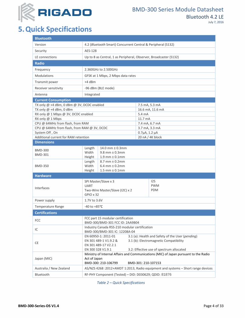
5. Quick Specifications Bluetooth
Version 4.2 (Bluetooth Smart) Concurrent Central & Peripheral (S132)
Security AES-128
LE connections Up to 8 as Central, 1 as Peripheral, Observer, Broadcaster (S132)
Radio
Frequency 2.360GHz to 2.500GHz
Modulations GFSK at 1 Mbps, 2 Mbps data rates
Transmit power +4 dBm
Receiver sensitivity -96 dBm (BLE mode)
Antenna Integrated
Current Consumption TX only @ +4 dBm, 0 dBm @ 3V, DCDC enabled 7.5 mA, 5.3 mA
TX only @ +4 dBm, 0 dBm 16.6 mA, 11.6 mA
RX only @ 1 Mbps @ 3V, DCDC enabled 5.4 mA
RX only @ 1 Mbps 11.7 mA
CPU @ 64MHz from flash, from RAM 7.4 mA, 6.7 mA
CPU @ 64MHz from flash, from RAM @ 3V, DCDC 3.7 mA, 3.3 mA
System Off , On 0.7µA, 1.2 µA
Additional current for RAM retention 20 nA / 4K block
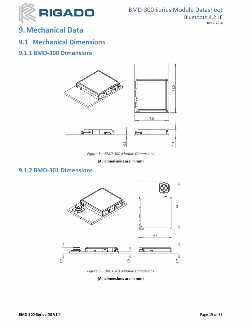
Dimensions
BMD-300 BMD-301
Length Width Height
14.0 mm ± 0.3mm 9.8 mm ± 0.3mm 1.9 mm ± 0.1mm
BMD-350 Length Width Height
8.7 mm ± 0.2mm 6.4 mm ± 0.2mm 1.5 mm ± 0.1mm
Hardware
Interfaces
SPI Master/Slave x 3 UART Two-Wire Master/Slave (I2C) x 2 GPIO x 32
I2S PWM PDM
Power supply 1.7V to 3.6V
Temperature Range -40 to +85°C
Certifications
FCC FCC part 15 modular certification BMD-300/BMD-301 FCC ID: 2AA9B04
IC Industry Canada RSS-210 modular certification BMD-300/BMD-301 IC: 12208A-04
CE
EN 60950-1: 2011-01 3.1 (a): Health and Safety of the User (pending) EN 301 489-1 V1.9.2 & 3.1 (b): Electromagnetic Compatibility EN 301 489-17 V2.2.1 EN 300 328 V1.9.1 3.2: Effective use of spectrum allocated
Japan (MIC) Ministry of Internal Affairs and Communications (MIC) of Japan pursuant to the Radio Act of Japan BMD-300: 210-106799 BMD-301: 210-107153
Australia / New Zealand AS/NZS 4268 :2012+AMDT 1:2013, Radio equipment and systems – Short range devices
Bluetooth RF-PHY Component (Tested) – DID: D030629; QDID: 81876
Table 2 – Quick Specifications
BMD-300 Series Module Datasheet Bluetooth 4.2 LE
July 7, 2016
BMD-300-Series-DS V1.4 Page 5 of 33
6. Pin Descriptions
6.1 BMD-300 / BMD-301
Figure 2 – BMD-300/301 Pin out (Top View)
Pin description
Pin Name Direction Description
6 P0.25 In/Out GPIO2
7 P0.26 In/Out GPIO2
8 P0.27 In/Out GPIO2
9 P0.28 In/Out GPIO/AIN42
10 P0.29 In/Out GPIO/AIN52
11 P0.30 In/Out GPIO/AIN62
12 P0.31 In/Out GPIO/AIN72
13 P0.00 In/Out GPIO/XTAL1 (32.768kHz)
14 P0.01 In/Out GPIO/XTAL2 (32.768kHz)
15 P0.02 In/Out GPIO/AIN0
19 P0.03 In/Out GPIO/AIN1
20 P0.04 In/Out GPIO/AIN2
21 P0.05 In/Out GPIO/AIN3
22 P0.06 In/Out GPIO
23 P0.07 In/Out GPIO
24 P0.08 In/Out GPIO
25 P0.09 In/Out GPIO/NFC1
26 P0.10 In/Out GPIO/NFC2
27 P0.11 In/Out GPIO
28 P0.12 In/Out GPIO
31 P0.13 In/Out GPIO
32 P0.14 In/Out GPIO/TRACEDATA[3]
33 P0.15 In/Out GPIO/TRACEDATA[2]
BMD-300 Series Module Datasheet Bluetooth 4.2 LE
July 7, 2016
BMD-300-Series-DS V1.4 Page 6 of 33
Pin Name Direction Description
34 P0.16 In/Out GPIO/TRACEDATA[1]
35 P0.17 In/Out GPIO
36 P0.18 In/Out GPIO/TRACEDATA[0]/SWO
37 P0.19 In/Out GPIO
38 P0.20 In/Out GPIO/TRACECLK
39 P0.21 In/Out GPIO/RESET
40 P0.22 In/Out GPIO2
41 P0.23 In/Out GPIO2
42 P0.24 In/Out GPIO2
43 SWCLK In SWD Clock
44 SWDIO In/Out SWD IO
17 VCC Power +1.7V to +3.6V1
1, 2, 3, 4, 5, 16, 18, 29, 30, 45, 46, 47
GND Power Electrical Ground
Note 1: An internal 4.7µF bulk capacitor is included on the module. However, it is good design practice to add additional bulk capacitance as required for your application, i.e. those with heavy GPIO usage and/or current draw.
Note 2: These pins are in close proximity to the nRF52 radio power supply and antenna pins. Radio performance parameters, such as sensitivity, may be affected by high frequency digital I/O with large sink/source current on these pins. Nordic recommends using only low frequency, low-drive functions when possible.
Table 3 – BMD-300/301 Pin Descriptions
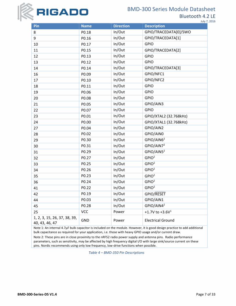
6.2 BMD-350
Figure 3 – BMD-350 Pin out (Top View)
Pin description
Pin Name Direction Description
4 SWCLK In SWD Clock
5 SWDIO In/Out SWD IO
6 P0.20 In/Out GPIO/TRACECLK
7 P0.21 In/Out GPIO
BMD-300 Series Module Datasheet Bluetooth 4.2 LE
July 7, 2016
BMD-300-Series-DS V1.4 Page 7 of 33
Pin Name Direction Description
8 P0.18 In/Out GPIO/TRACEDATA[0]/SWO
9 P0.16 In/Out GPIO/TRACEDATA[1]
10 P0.17 In/Out GPIO
11 P0.15 In/Out GPIO/TRACEDATA[2]
12 P0.13 In/Out GPIO
13 P0.12 In/Out GPIO
14 P0.14 In/Out GPIO/TRACEDATA[3]
16 P0.09 In/Out GPIO/NFC1
17 P0.10 In/Out GPIO/NFC2
18 P0.11 In/Out GPIO
19 P0.06 In/Out GPIO
20 P0.08 In/Out GPIO
21 P0.05 In/Out GPIO/AIN3
22 P0.07 In/Out GPIO
23 P0.01 In/Out GPIO/XTAL2 (32.768kHz)
24 P0.00 In/Out GPIO/XTAL1 (32.768kHz)
27 P0.04 In/Out GPIO/AIN2
28 P0.02 In/Out GPIO/AIN0
29 P0.30 In/Out GPIO/AIN62
30 P0.31 In/Out GPIO/AIN72
31 P0.29 In/Out GPIO/AIN52
32 P0.27 In/Out GPIO2
33 P0.25 In/Out GPIO2
34 P0.26 In/Out GPIO2
35 P0.23 In/Out GPIO2
36 P0.24 In/Out GPIO2
41 P0.22 In/Out GPIO2
42 P0.19 In/Out GPIO/RESET
44 P0.03 In/Out GPIO/AIN1
45 P0.28 In/Out GPIO/AIN42
25 VCC Power +1.7V to +3.6V1
1, 2, 3, 15, 26, 37, 38, 39, 40, 43, 46, 47
GND Power Electrical Ground
Note 1: An internal 4.7µF bulk capacitor is included on the module. However, it is good design practice to add additional bulk capacitance as required for your application, i.e. those with heavy GPIO usage and/or current draw.
Note 2: These pins are in close proximity to the nRF52 radio power supply and antenna pins. Radio performance parameters, such as sensitivity, may be affected by high frequency digital I/O with large sink/source current on these pins. Nordic recommends using only low frequency, low-drive functions when possible.
Table 4 – BMD-350 Pin Descriptions
BMD-300 Series Module Datasheet Bluetooth 4.2 LE
July 7, 2016
BMD-300-Series-DS V1.4 Page 8 of 33
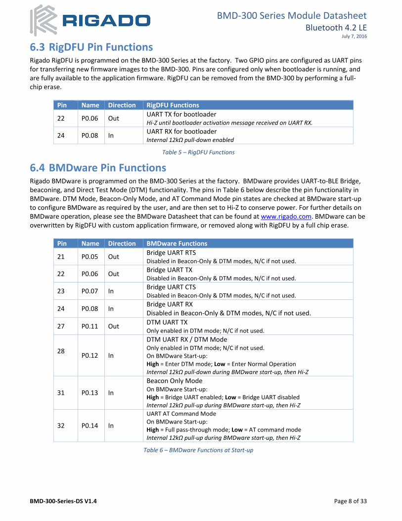
6.3 RigDFU Pin Functions Rigado RigDFU is programmed on the BMD-300 Series at the factory. Two GPIO pins are configured as UART pins for transferring new firmware images to the BMD-300. Pins are configured only when bootloader is running, and are fully available to the application firmware. RigDFU can be removed from the BMD-300 by performing a full-chip erase.
Pin Name Direction RigDFU Functions
22 P0.06 Out UART TX for bootloader Hi-Z until bootloader activation message received on UART RX.
24 P0.08 In UART RX for bootloader Internal 12kΩ pull-down enabled
Table 5 – RigDFU Functions
6.4 BMDware Pin Functions Rigado BMDware is programmed on the BMD-300 Series at the factory. BMDware provides UART-to-BLE Bridge, beaconing, and Direct Test Mode (DTM) functionality. The pins in Table 6 below describe the pin functionality in BMDware. DTM Mode, Beacon-Only Mode, and AT Command Mode pin states are checked at BMDware start-up to configure BMDware as required by the user, and are then set to Hi-Z to conserve power. For further details on BMDware operation, please see the BMDware Datasheet that can be found at www.rigado.com. BMDware can be overwritten by RigDFU with custom application firmware, or removed along with RigDFU by a full chip erase.
Pin Name Direction BMDware Functions
21 P0.05 Out Bridge UART RTS Disabled in Beacon-Only & DTM modes, N/C if not used.
22 P0.06 Out Bridge UART TX Disabled in Beacon-Only & DTM modes, N/C if not used.
23 P0.07 In Bridge UART CTS Disabled in Beacon-Only & DTM modes, N/C if not used.
24 P0.08 In Bridge UART RX Disabled in Beacon-Only & DTM modes, N/C if not used.
27 P0.11 Out DTM UART TX Only enabled in DTM mode; N/C if not used.
28
P0.12 In
DTM UART RX / DTM Mode Only enabled in DTM mode; N/C if not used. On BMDware Start-up: High = Enter DTM mode; Low = Enter Normal Operation Internal 12kΩ pull-down during BMDware start-up, then Hi-Z
31 P0.13 In
Beacon Only Mode On BMDware Start-up: High = Bridge UART enabled; Low = Bridge UART disabled Internal 12kΩ pull-up during BMDware start-up, then Hi-Z
32 P0.14 In
UART AT Command Mode On BMDware Start-up: High = Full pass-through mode; Low = AT command mode Internal 12kΩ pull-up during BMDware start-up, then Hi-Z
7.1 Absolute Maximum Ratings Symbol Parameter Min. Max. Unit
VCC_MAX Voltage on supply pin -0.3 3.9 V
VIO_MAX Voltage on GPIO pins (VCC > 3.6V) -0.3 3.9 V
VIO_MAX Voltage on GPIO pins (VCC ≤ 3.6V) -0.3 VCC + 0.3V V
TS Storage Temperature Range -40 125 °C
Table 7 – Absolute Maximum Ratings
7.2 Operating Conditions Symbol Parameter Min. Typ. Max. Unit
VCC Operating supply voltage 1.7 3.0 3.6 V
TR_VCC Supply rise time (0V to 1.7V) - - 60 ms
TA Operating Ambient Temperature Range -40 25 85 °C
Table 8 – Operating Conditions
7.3 General Purpose I/O The general purpose I/O is organized as one port enabling access and control of the 32 available GPIO pins through one port. Each GPIO can be accessed individually with the following user configurable features:
Input/output direction
Output drive strength
Internal pull-up and pull-down resistors
Wake-up from high or low level triggers on all pins
Trigger interrupt on all pins
All pins can be used by the PPI task/event system; the maximum number of pins that can be interfaced through the PPI at the same time is limited by the number of GPIOTE channels
All pins can be individually configured to carry serial interface or quadrature demodulator signals
Symbol Parameter Min. Typ. Max. Unit
VIH Input High Voltage 0.7 x VCC - VCC V
VIL Input Low Voltage VSS - 0.3 x VCC V
VOH Output High Voltage VCC − 0.4 - VCC V
VOL Output Low Voltage VSS - VSS + 0.4 V
RPU Pull-up Resistance 11 13 16 kΩ
RPD Pull-down Resistance 11 13 16 kΩ
Table 9 – GPIO
7.4 Module RESET GPIO pin P0.21 may be used for a hardware reset. In order to utilize P0.21 as a hardware reset, the UICR registers PSELRESET[0] and PSELRESET[1] must be set alike, to the value of 0x7FFFFF15. When P0.21 is programmed as RESET , the internal pull-up is automatically enabled. Rigado and Nordic example applications and development kits program P0.21 as RESET .
BMD-300 Series Module Datasheet Bluetooth 4.2 LE
July 7, 2016
BMD-300-Series-DS V1.4 Page 10 of 33
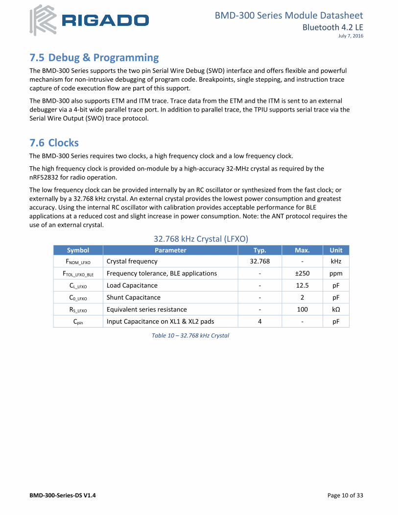
7.5 Debug & Programming The BMD-300 Series supports the two pin Serial Wire Debug (SWD) interface and offers flexible and powerful mechanism for non-intrusive debugging of program code. Breakpoints, single stepping, and instruction trace capture of code execution flow are part of this support.
The BMD-300 also supports ETM and ITM trace. Trace data from the ETM and the ITM is sent to an external debugger via a 4-bit wide parallel trace port. In addition to parallel trace, the TPIU supports serial trace via the Serial Wire Output (SWO) trace protocol.
7.6 Clocks The BMD-300 Series requires two clocks, a high frequency clock and a low frequency clock.
The high frequency clock is provided on-module by a high-accuracy 32-MHz crystal as required by the nRF52832 for radio operation.
The low frequency clock can be provided internally by an RC oscillator or synthesized from the fast clock; or externally by a 32.768 kHz crystal. An external crystal provides the lowest power consumption and greatest accuracy. Using the internal RC oscillator with calibration provides acceptable performance for BLE applications at a reduced cost and slight increase in power consumption. Note: the ANT protocol requires the use of an external crystal.
32.768 kHz Crystal (LFXO) Symbol Parameter Typ. Max. Unit
FNOM_LFXO Crystal frequency 32.768 - kHz
FTOL_LFXO_BLE Frequency tolerance, BLE applications - ±250 ppm
CL_LFXO Load Capacitance - 12.5 pF
C0_LFXO Shunt Capacitance - 2 pF
RS_LFXO Equivalent series resistance - 100 kΩ
Cpin Input Capacitance on XL1 & XL2 pads 4 - pF
Table 10 – 32.768 kHz Crystal
BMD-300 Series Module Datasheet Bluetooth 4.2 LE
July 7, 2016
BMD-300-Series-DS V1.4 Page 11 of 33
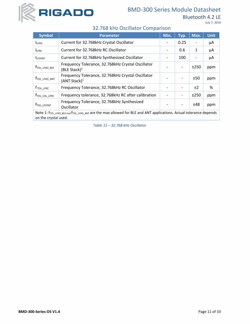
32.768 kHz Oscillator Comparison Symbol Parameter Min. Typ. Max. Unit
ILFXO Current for 32.768kHz Crystal Oscillator - 0.25 - µA
ILFRC Current for 32.768kHz RC Oscillator - 0.6 1 µA
ILFSYNT Current for 32.768kHz Synthesized Oscillator - 100 - µA
fTOL_LFXO_BLE Frequency Tolerance, 32.768kHz Crystal Oscillator (BLE Stack)1
- - ±250 ppm
fTOL_LFXO_ANT Frequency Tolerance, 32.768kHz Crystal Oscillator (ANT Stack)1
- - ±50 ppm
f TOL_LFRC Frequency Tolerance, 32.768kHz RC Oscillator - - ±2 %
fTOL_CAL_LFRC Frequency tolerance, 32.768kHz RC after calibration - - ±250 ppm
fTOL_LFSYNT Frequency Tolerance, 32.768kHz Synthesized Oscillator
- - ±48 ppm
Note 1: fTOL_LFXO_BLE and fTOL_LFXO_ANT are the max allowed for BLE and ANT applications. Actual tolerance depends on the crystal used.
Table 11 – 32.768 kHz Oscillator
BMD-300 Series Module Datasheet Bluetooth 4.2 LE
July 7, 2016
BMD-300-Series-DS V1.4 Page 12 of 33
8. Firmware
8.1 Factory Image All modules are shipped with factory programmed firmware. The factory programmed firmware version is indicated on the label.
8.1.1 Firmware Version ‘AA’ Factory firmware version ‘AA’ contains the Rigado RigDFU OTA and Serial bootloader v3.2.0 (42), Nordic S132 SoftDevice v2.0.0, and Rigado BMDware v3.1.0 (50). Modules can be programmed with customer code via BLE and UART interfaces using the bootloader and Rigado provided tools, or with a full-chip erase via the SWD interface. Examples apps for iOS and Android are provided that utilize the Rigablue Library for easy OTA updates. Visit the BMD Software Suite page at www.rigado.com for more information. Note: A full chip erase will clear the Rigado assigned MAC address from memory; see section 8.3 “MAC Address Info” on how to retain it.
8.1.2 Firmware Version ‘AB’ Factory firmware version ‘AB’ contains the Rigado RigDFU OTA and Serial bootloader v3.2.1 (43), Nordic S132 SoftDevice v2.0.0, and Rigado BMDware v3.1.1 (51). Modules can be programmed with customer code via BLE and UART interfaces using the bootloader and Rigado provided tools, or with a full-chip erase via the SWD interface. Examples apps for iOS and Android are provided that utilize the Rigablue Library for easy OTA updates. Visit the BMD Software Suite page at www.rigado.com for more information. Note: A full chip erase will clear the Rigado assigned MAC address from memory; see section 8.3 “MAC Address Info” on how to retain it.
8.1.3 Module Programming and Read-Back Protection RigDFU allows for UART and OTA updates to RigDFU, the SoftDevice and application firmware. Read-back protection of the BMD-300 Series modules is enabled which prevents unauthorized access to the firmware and optional encryption keys through the SWD debug port. If the SWD port is required, for example when developing custom firmware, the nRF52 must be erased and recovered. This is accomplished with the Rigado BMD-300 Eraser and Recovery Utility at www.rigado.com, or with nrfjprog, which is provided with the Nordic Semiconductor command line utilities:
nrfjprog -f NRF52 ––recover
A full chip erase is performed, so all components will need re-loaded (RigDFU Bootloader, SoftDevice and application Firmware). The rigado/bootloader-tools repository on GitHub contains the utilities to load these items. Procedures are described in the RigDFU Datasheet at www.rigado.com for programming, firmware preparation, and update procedures. The BMD-300 Series modules may also be restored to the factory firmware versions noted above with the utilities available at the rigado/programming repository on GitHub. Access to the Rigado BMD Software Suite may be requested on the Rigado Website.
8.2 SoftDevices Nordic Semiconductor protocol stacks are known as SoftDevices. SoftDevices are pre-compiled, pre-linked binary files. SoftDevices can be programmed in nRF52 series SoCs and are downloadable from the Nordic website. The BMD-300 with the nRF52832 SoC supports the S132 (BLE Central & Peripheral), S212 (ANT) and S312 (ANT and BLE) SoftDevices.
8.2.1 S132 The S132 SoftDevice is a Bluetooth® low energy (BLE) Central and Peripheral protocol stack solution supporting up to three Central and one Peripheral simultaneous connections and concurrent Observer and Broadcaster roles. It integrates a low energy Controller and Host, and provides a full and flexible API for building Bluetooth low energy System on Chip (SoC) solutions. Key Features
Bluetooth 4.2 compliant low energy single-mode
protocol stack suitable for Bluetooth Smart products
Concurrent Central, Observer, Peripheral, and
Broadcaster roles with up to:
o Three connections as a central
o One connection as a peripheral
o Observer
o Broadcaster
Link layer
L2CAP, ATT, and SM protocols
GATT and GAP APIs
GATT Client and Server
Complementary nRF52 SDK including Bluetooth profiles
and example applications
Master Boot Record for over-the-air device firmware
update
Memory isolation between application and protocol
stack for robustness and security
Thread-safe supervisor-call based API
Asynchronous, event-driven behavior
No RTOS dependency
o Any RTOS can be used
No link-time dependencies
o Standard ARM® CortexTMM4F project
configuration for application development
Support for concurrent and non-concurrent
multiprotocol operation
o Concurrent with the Bluetooth stack using
concurrent multiprotocol timeslot API
Alternate protocol stack in application space
8.2.2 S212 The S212 SoftDevice is an ANT protocol stack solution that provides a full and flexible Application Programming Interface (API) for building ANT System on Chip (SoC) solutions for the nRF52832 chip. The S212 SoftDevice simplifies combining the ANT protocol stack and an application on the same CPU. Key Features
Advanced ANT stack
Simple to complex network topologies:
o Peer-to-peer, Star, Tree, Star-to-star and
more
Up to 15 logical channels, each with configurable:
o Channel type, ID and period
o RF frequency
o Networks
Broadcast, Acknowledged, and Burst Data modes
Device search, pairing and proximity support
Enhanced ANT features:
o Advanced Burst Transfer mode (up to 60
kbps)
o Up to 15 channels encryption (AES-128)
support
o Additional networks – up to 8
o Event Filtering and Selective Data Updates
o Asynchronous Transmission
o Fast Channel Initiation
BMD-300 Series Module Datasheet Bluetooth 4.2 LE
July 7, 2016
BMD-300-Series-DS V1.4 Page 14 of 33
SoftDevice features
Built-in NVM access and radio coexistence
management
Master Boot Record for over-the air device firmware
update
Memory isolation between application and protocol
stack for robustness and security
Thread-safe supervisor-call based API
Asynchronous, event-driven behavior
No RTOS dependency
o Any RTOS can be used
o No link-time dependencies
o Standard ARM® Cortex™ -M4F project
configuration for application development
Support for concurrent and non-concurrent
multiprotocol operation
Concurrent multiprotocol timeslot API
Alternate protocol stack running in application space
8.2.3 S332 The S332 SoftDevice is a combined ANT™ and Bluetooth® low energy (BLE) protocol stack solution. It supports all four Bluetooth low energy roles (central, peripheral, observer, broadcaster) and ANT. The S332 SoftDevice provides a full and flexible Application Programming Interface (API) for building concurrent ANT and BLE System on Chip (SoC) solutions. It simplifies combining an ANT and BLE protocol stack and an application on the same CPU, therefore eliminating the need for an added device to support concurrent multiprotocol.
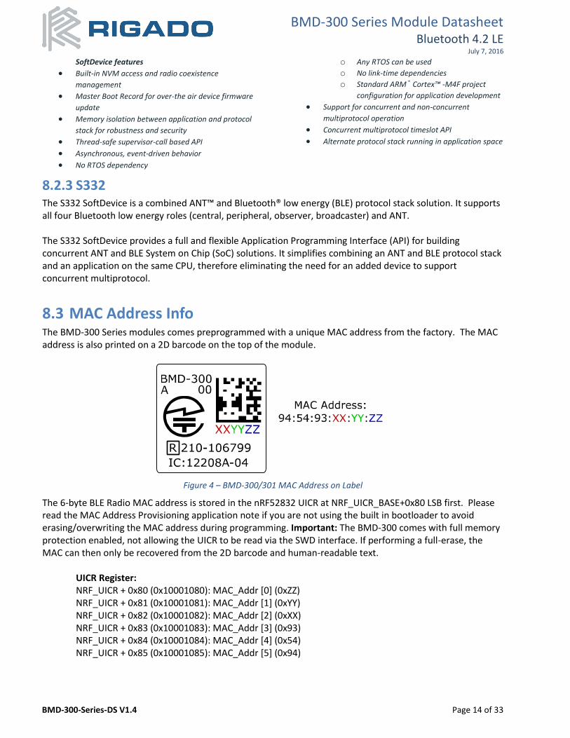
8.3 MAC Address Info The BMD-300 Series modules comes preprogrammed with a unique MAC address from the factory. The MAC address is also printed on a 2D barcode on the top of the module.
Figure 4 – BMD-300/301 MAC Address on Label
The 6-byte BLE Radio MAC address is stored in the nRF52832 UICR at NRF_UICR_BASE+0x80 LSB first. Please read the MAC Address Provisioning application note if you are not using the built in bootloader to avoid erasing/overwriting the MAC address during programming. Important: The BMD-300 comes with full memory protection enabled, not allowing the UICR to be read via the SWD interface. If performing a full-erase, the MAC can then only be recovered from the 2D barcode and human-readable text.
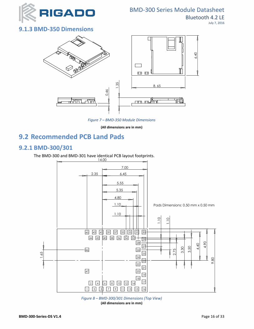
9.2.1 BMD-300/301 The BMD-300 and BMD-301 have identical PCB layout footprints.
Figure 8 – BMD-300/301 Dimensions (Top View)
(All dimensions are in mm)
BMD-300 Series Module Datasheet Bluetooth 4.2 LE
July 7, 2016
BMD-300-Series-DS V1.4 Page 17 of 33
9.2.2 BMD-350
Figure 9 – BMD-350 Dimensions (Top View)
(All dimensions are in mm)
10. Module Marking
10.1 BMD-300 Module Marking
Figure 10 – BMD-300 Module Marking – Rev A
BMD-300 Series Module Datasheet Bluetooth 4.2 LE
July 7, 2016
BMD-300-Series-DS V1.4 Page 18 of 33
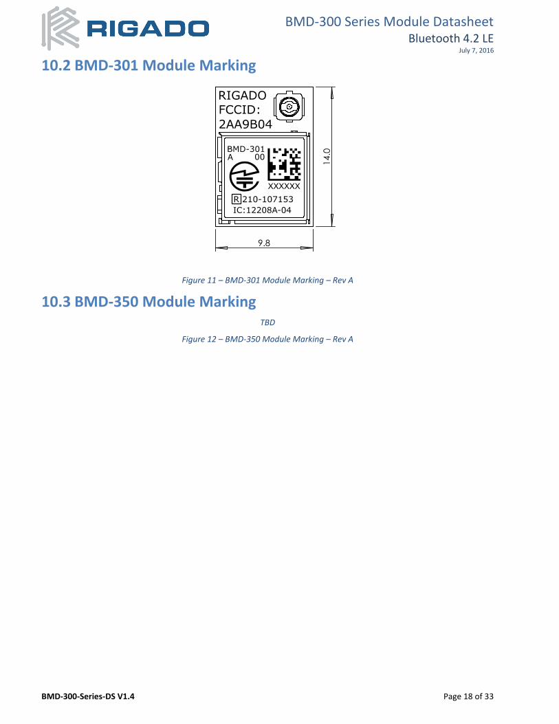
10.2 BMD-301 Module Marking
Figure 11 – BMD-301 Module Marking – Rev A
10.3 BMD-350 Module Marking TBD
Figure 12 – BMD-350 Module Marking – Rev A
BMD-300 Series Module Datasheet Bluetooth 4.2 LE
July 7, 2016
BMD-300-Series-DS V1.4 Page 19 of 33
11. RF Design Notes
11.1 Recommended RF Layout & Ground Plane
11.1.1 BMD-300 For the BMD-300, the integrated antenna requires a suitable ground plane to radiate effectively. The area under and extending out from the antenna portion of the module should be kept clear of copper and other metal. The module should be placed at the edge of the PCB with the antenna edge facing out. Reducing the ground plane from that shown in Figure 13 will reduce the effective radiated power. For example, a 27mm x 29mm board (about the size of a coin cell) has approximately 3dB lower output than the BMD-300 Evaluation Board.
Figure 13 – BMD-300 Recommended RF Layout
11.1.2 BMD-301 For the BMD-301, refer to the external antenna datasheet for antenna placement and grounding recommendations.
11.1.3 BMD-350 For the BMD-305, the integrated chip antenna requires a suitable ground plane to radiate effectively. The area under and extending out from the antenna portion of the module should be kept clear of copper and other metal. The module should be placed at the edge of the PCB with the antenna edge facing out.
Drawing TBD
Figure 14 – BMD-350 Recommended RF Layout
BMD-300 Series Module Datasheet Bluetooth 4.2 LE
July 7, 2016
BMD-300-Series-DS V1.4 Page 20 of 33
11.2 Mechanical Enclosure For the BMD-300 and BMD-350, care should be taken when designing and placing the module into an enclosure. Metal should be kept clear from the antenna area, both above and below. Any metal around the module can negatively impact RF performance. The module is designed and tuned for the antenna and RF components to be in free air. Any potting, epoxy fill, plastic over-molding, or conformal coating can negatively impact RF performance and must be evaluated by the customer. For the BMD-301, refer to the external antenna datasheet for placement in or on a mechanical enclosure.
BMD-300 Series Module Datasheet Bluetooth 4.2 LE
July 7, 2016
BMD-300-Series-DS V1.4 Page 21 of 33
11.3 Antenna Patterns
11.3.1 BMD-300 Antenna patterns are based off of the BMD-300 Evaluation Kit Version A with a ground plane size of 82mm x 56mm. X-Y-Z orientation is shown in Figure 15:
Figure 15 – X-Y-Z Antenna Orientation
11.3.1.1 X-Y Plane
Figure 16 – X-Y Plane Antenna Pattern
X Y
BMD-300 Series Module Datasheet Bluetooth 4.2 LE
July 7, 2016
BMD-300-Series-DS V1.4 Page 22 of 33
11.3.1.2 Y-Z Plane
Figure 17 – Y-Z Plane Antenna Pattern
11.3.1.3 Z-X Plane
Figure 18 – Z-X Plane Antenna Pattern
Z X
Y Z
BMD-300 Series Module Datasheet Bluetooth 4.2 LE
July 7, 2016
BMD-300-Series-DS V1.4 Page 23 of 33
11.3.2 BMD-350
11.3.2.1 X-Y Plane
Figure 19 – X-Y Plane Antenna Pattern
11.3.2.2 Y-Z Plane
Figure 20 – Y-Z Plane Antenna Pattern
BMD-300 Series Module Datasheet Bluetooth 4.2 LE
July 7, 2016
BMD-300-Series-DS V1.4 Page 24 of 33
11.3.2.3 Z-X Plane
Figure 21 – Z-X Plane Antenna Pattern
12. Evaluation Boards Rigado has developed full featured evaluation boards that provide a complete I/O pin out to headers, on-board programming and debug, 32.768 kHz crystal, power & virtual COM port over USB, 4 user LEDs, and 4 user buttons. The evaluation boards also provide the option to be powered from a CR2032 coin cell battery, and have current sense resistors and headers to allow for convenient current measurements. An Arduino Uno R3 style header is provided for easy prototyping of additional functions. The evaluation boards also support programming off-board BMD-300 Series modules. Evaluation kits are available
13. Custom Development Rigado is a full-service design house offering end-to-end product development from concept to manufacturing. We can provide custom modules and do electrical and mechanical design, end product manufacturing, firmware and mobile development, and web and cloud integration. Please contact Rigado at [email protected] or 1-866-6-RIGADO for custom engineering options and fees.
14. Bluetooth Qualification The BMD-300 Series modules are qualified as a Bluetooth Component (tested) for RF-PHY. This allows customers to use different SoftDevices that have been qualified by Nordic without the need to complete additional RF-PHY testing. To achieve Bluetooth End Product qualification, the Rigado RF-PHY QDID can be combined with Nordic QDIDs for the SoftDevice used when filing on the Bluetooth SIG website. The only testing required is for the Bluetooth profiles supported by the customer’s product. Products with only custom profiles do not require any additional testing.
BMD-300/BMD-301: Declaration ID D030629 / QDID 81876
BMD-350: Declaration ID TBD / QDID TBD
15. Regulatory Statements Note: All certifications for the BMD-350 are pending.
15.1 FCC Statement: This device has been tested and found to comply with part 15 of the FCC rules. These limits are designed to provide reasonable protection against harmful interference in a residential installation. This equipment generates, uses and can radiate radio frequency energy and, if not installed and used in accordance with the instructions, may cause harmful interference to radio communications. However, there is no guarantee that interference will not occur in a particular installation. If this equipment does cause harmful interference to radio or television reception, which can be determined by turning the equipment off and on, the user is encouraged to try to correct the interference by one or more of the following measures:
Reorient or relocate the receiving antenna.
Increase the separation between the equipment and the receiver
Connect the equipment into an outlet on a circuit different from that to which the receiver is connected.
Consult the dealer or an experienced radio/TV technician for help. Operation is subjected to the following two conditions: (1) This device may no cause harmful interference, and (2) this device must accept any interference received, including interference that may cause undesired operation. Note: Modification to this product will void the user’s authority to operate this equipment. Note: Modification to this product will void the users’ authority to operate this equipment.
15.2 FCC Important Notes: (1) FCC Radiation Exposure Statement This equipment complies with FCC RF radiation exposure limits set forth for an uncontrolled environment. This transmitter must not be co-located or operating in conjunction with any other antenna or transmitter. This equipment complies with Part 15 of the FCC Rules. Operation is subject the following two conditions: (1) This device may not cause harmful interference, and (2) This device must accept any interference received, including interference that may cause undesired operation. The devices must be installed and used in strict accordance with the manufacturer’s instructions as described in this document. Caution! The manufacturer is not responsible for any radio or TV interference caused by unauthorized modifications to
BMD-300 Series Module Datasheet Bluetooth 4.2 LE
July 7, 2016
BMD-300-Series-DS V1.4 Page 26 of 33
this equipment. Such modification could void the user authority to operate the equipment.
(2) Co-location Warning: This device and its antenna(s) must not be co-located or operating in conjunction with any other transmitter antenna.
(3) OEM integration instructions: This device is intended only for OEM integrators under the following conditions: The antenna and transmitter must not be co-located with any other transmitter or antenna. The module shall be only used with the integral antenna(s) that has been originally tested and certified with this module. As long as the two (2) conditions above are met, further transmitter testing will not be required. However, the OEM integrator is still responsible for testing their end-product for any additional compliance requirements with this module installed (for example, digital device emission, PC peripheral requirements, etc.) In the event that these conditions cannot be met (for example certain laptop configuration or co-location with another transmitter), then the FCC authorization for this module in combination with the host equipment is no longer considered valid and the FCC ID of the module cannot be used on the final product. In these and circumstance, the OEM integrator will be responsible for re-evaluating. The end product (including the transmitter) and obtaining a separate FCC authorization. Caution! The OEM is still responsible for verifying compliance with FCC Part 15, subpart B limits for unintentional radiators through an accredited test facility.
(4) End product labeling: The final end product must be labeled in a visible area with the following:
BMD-300: “Contains FCC ID: 2AA9B04”
BMD-301: “Contains FCC ID: 2AA9B04”
BMD-350: “Contains FCC ID: TBD” (pending)
Any similar wording that expresses the same meaning may be used. The FCC Statement below should also be included on the label. When not possible, the FCC Statement should be included in the User Manual of the host device.
“This device complies with part 15 of the FCC rules. Operation is subject to the following two conditions. (1) This device may not cause harmful interference. (2) This device must accept any interference received, including interference that may cause undesired operation.”
(5) Information regarding the end user manual: The OEM integrator has to be aware not to provide information to the end user regarding how to install or remove this RF module in the user’s manual of the end product which integrates this module. The end user manual shall include all required regulatory information/warning as show in this manual (Section 15.2(4)).
BMD-300 Series Module Datasheet Bluetooth 4.2 LE
July 7, 2016
BMD-300-Series-DS V1.4 Page 27 of 33
15.3 IC Statement: This device complies with Industry Canada license-exempt RSS standard(s). Operation is subject to the following two conditions: (1) this device may not cause interference, and (2) this device must accept any interference, including interference that may cause undesired operation of the device. Le présent appareil est conforme aux CNR d'Industrie Canada applicables aux appareils radio exempts de licence. L'exploitation est autorisée aux deux conditions suivantes : (1) l'appareil ne doit pas produire de brouillage, et (2) l'utilisateur de l'appareil doit accepter tout brouillage radioélectrique subi, même si le brouillage est susceptible d'en compromettre le fonctionnement. RF exposure warning: The equipment complies with RF exposure limits set forth for an uncontrolled environment. The antenna(s) used for this transmitter must not be co-located or operating in conjunction with any other antenna or transmitter. Avertissement d'exposition RF: L'équipement est conforme aux limites d'exposition aux RF établies pour un incontrôlés environnement. L'antenne (s) utilisée pour ce transmetteur ne doit pas être co-localisés ou onctionner en conjonction avec toute autre antenne ou transmetteur .
15.4 IC Important Notes: 1. The OEM integrator has to be aware not to provide information to the end user regarding how to install or remove this RF module in the user manual of the end product. The user manual which is provided by OEM integrators for end users must include the following information in a prominent location. 2. To comply with IC RF exposure compliance requirements, the antenna used for this transmitter must not be co‐located or operating in conjunction with any other antenna or transmitter, except in accordance with IC multi‐transmitter product procedures. 3. The final system integrator must ensure there is no instruction provided in the user manual or customer documentation indicating how to install or remove the transmitter module except such device has implemented two‐ways authentication between module and the host system. 4. The host device shall be properly labelled to identify the module within the host device. The final end product must be labeled in a visible area with the following:
BMD-300: “Contains IC: 12208A-04“
BMD-301: “Contains IC: 12208A-04“
BMD-350: “Contains IC: TBD“ (pending) Any similar wording that expresses the same meaning may be used. The IC Statement below should also be included on the label. When not possible, the IC Statement should be included in the User Manual of the host device.
“This device complies with Industry Canada license-exempt RSS standard(s). Operation is subject to the following two conditions: (1) this device may not cause interference, and (2) this device must accept any interference, including interference that may cause undesired operation of the device. Le présent appareil est conforme aux CNR d'Industrie Canada applicables aux appareils radio exempts de licence. L'exploitation est autorisée aux deux conditions suivantes : (1) l'appareil ne doit pas produire de brouillage, et (2) l'utilisateur de l'appareil doit accepter tout brouillage radioélectrique subi, même si le brouillage est susceptible d'en compromettre le onctionnement.”
BMD-300 Series Module Datasheet Bluetooth 4.2 LE
July 7, 2016
BMD-300-Series-DS V1.4 Page 28 of 33
15.5 CE Regulatory: The BMD-300 Series modules are tested and compliant against the following standards. OEM integrators should consult with qualified test house to verify all regulatory requirements have been met for their complete device. Note: Certifications for the BMD-350 are pending. From Directive 2006/95/EC:
EN 60950-1: 2006 + A11: 2009 + A1: 2010 + A12: 2011 (pending) From R&TTE Directive 1999/5/EC:
ETSI EN 300 328 V 1.9.1 From Directive 2004/108/EC:
ETSI EN 301 489-1 V1.9.2
ETSI EN 301 489-17 V2.2.1 Declarations of Conformity and supporting test reports are available at www.rigado.com.
15.6 Japan (MIC) The BMD-300 Series modules have received type certification and is labeled with its own technical conformity mark and certification number as required to conform to the technical standards regulated by the Ministry of Internal Affairs and Communications (MIC) of Japan pursuant to the Radio Act of Japan. Integration of this module into a final end product does not require additional radio certification provided installation instructions are followed and no modifications of the module are allowed. Additional testing may be required:
• If the host product is subject to electrical appliance safety (for example, powered from an AC mains), the host product may require Product Safety Electrical Appliance and Material (PSE) testing. The integrator should contact their conformance laboratory to determine if this testing is required.
• There is a voluntary Electromagnetic Compatibility (EMC) test for the host product administered by VCCI: http://www.vcci.jp/vcci_e/index.html
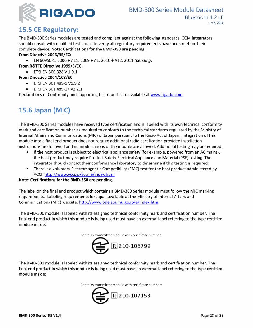
Note: Certifications for the BMD-350 are pending. The label on the final end product which contains a BMD-300 Series module must follow the MIC marking requirements. Labeling requirements for Japan available at the Ministry of Internal Affairs and Communications (MIC) website: http://www.tele.soumu.go.jp/e/index.htm. The BMD-300 module is labeled with its assigned technical conformity mark and certification number. The final end product in which this module is being used must have an external label referring to the type certified module inside:
Contains transmitter module with certificate number:
The BMD-301 module is labeled with its assigned technical conformity mark and certification number. The final end product in which this module is being used must have an external label referring to the type certified module inside:
Contains transmitter module with certificate number:
15.7 Australia / New Zealand Note: Certifications for the BMD-350 are pending. The BMD-300 Series modules have been tested to comply with the AS/NZS 4268 :2012+AMDT 1:2013, Radio equipment and systems – Short range devices – Limits and methods of measurement. The report may be downloaded from www.rigado.com, and may be used as evidence in obtaining permission to use the RCM. Information on registration as a Responsible Party, license and labeling requirements may be found at the following websites: Australia: http://www.acma.gov.au/theACMA/radiocommunications-short-range-devices-standard-2004
New Zealand: http://www.rsm.govt.nz/compliance The A-Tick and C-Tick marks are being migrated to the Regulatory Compliance Mark (RCM). Only Australian-based and New Zealand-based companies who are registered may be granted permission to use the RCM. An Australian-based or New Zealand-based agent or importer may also register as a Responsible Party to use the RCM on behalf of a company not in Australia or New Zealand.
15.8 Approved External Antennas The antennas listed below were tested for use with the BMD-301.
# Manufacturer Part Number Max Gain Type Size Approvals
16.1 Moisture Sensitivity Level The BMD-300 Series is rated for MSL 3, 168-hour floor life after opening.
17. Packaging and Labeling
17.1 Carrier Tape Dimensions
17.1.1 BMD-300 & BMD-301
Figure 23 – Carrier Tape Dimensions
BMD-300 Series Module Datasheet Bluetooth 4.2 LE
July 7, 2016
BMD-300-Series-DS V1.4 Page 31 of 33
17.1.2 BMD-350 Carrier tape dimensions are TBD.
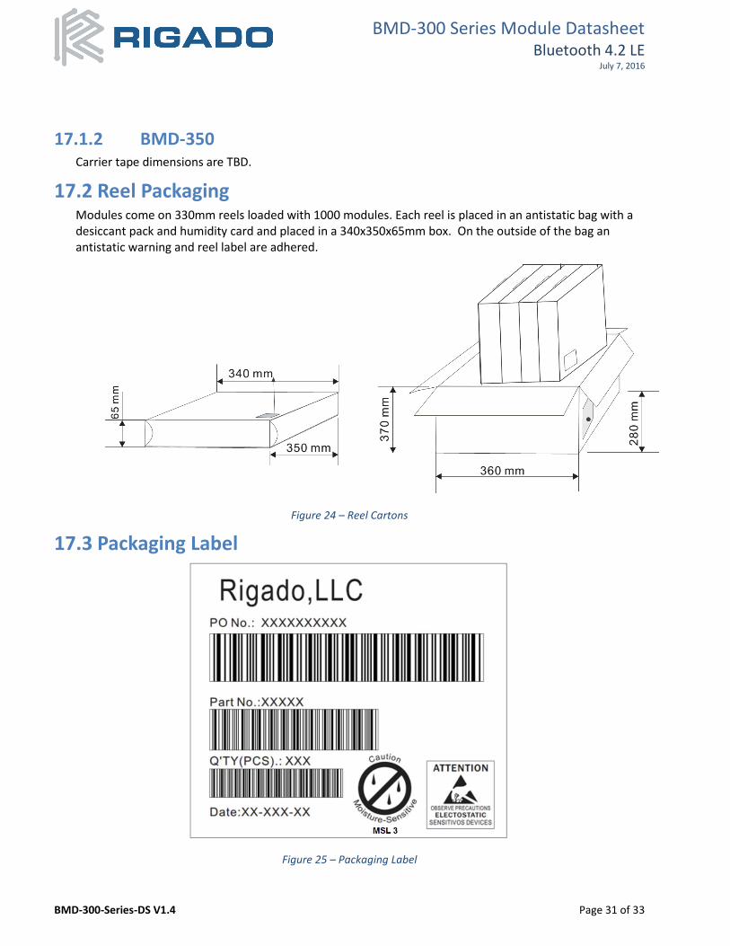
17.2 Reel Packaging Modules come on 330mm reels loaded with 1000 modules. Each reel is placed in an antistatic bag with a desiccant pack and humidity card and placed in a 340x350x65mm box. On the outside of the bag an antistatic warning and reel label are adhered.
Figure 24 – Reel Cartons
17.3 Packaging Label
Figure 25 – Packaging Label
BMD-300 Series Module Datasheet Bluetooth 4.2 LE
July 7, 2016
BMD-300-Series-DS V1.4 Page 32 of 33
18. Cautions 1) The guidelines of this document should be followed in order to assure proper performance of the
module. 2) This product is for use in office, business, and residential applications, but not medical devices. 3) This module may short-circuit. If a short circuit can result in serious damage or injury then failsafe
precautions should be used. This could be accomplished by redundant systems and protection circuits. 4) Supply voltage to the module should not be higher than the specified inputs or reversed. Additionally,
it should not contain noise, spikes, or AC ripple voltage. 5) Avoid use with other high frequency circuits. 6) Use methods to eliminate static electricity when working with the module as it can damage the
components. 7) Contact with wires, the enclosure, or any other objects should be avoided. 8) Refer to the recommended pattern when designing for this module. 9) If hand soldering is used, be sure to use the precautions outlined in this document. 10) This module should be kept away from heat, both during storage and after installation. 11) Do not drop or physically shock the module. 12) Do not damage the interface surfaces of the module. 13) The module should not be mechanically stressed at any time (storage, handling, installation). 14) Do not store or expose this module to:
Humid or salty air conditions
High concentrations of corrosive gasses.
Long durations of direct sunlight.
Temperatures lower than -40°C or higher than 125°C.
19. Life Support Policy This product is not designed to be used in a life support device or system, or in applications where there is potential for a failure or malfunction to, directly or indirectly, cause significant injury. By using this product in an application that poses these risks, such as described above, the customer is agreeing to indemnify Rigado for any damages that result.
20. Document History Revision Date Changes / Notes