Page 1
AP3585 Document number: DS36790 Rev. 1 - 2
1 of 16 www.diodes.com
April 2014 © Diodes Incorporated
AP3585
A Product Line of
Diodes Incorporated
SINGLE PHASE SYNCHRONOUS BUCK PWM CONTROLLER
Description
The AP3585 is a synchronous-rectified buck controller specifically
designed to operate from 4.5V to 13.2V supply voltage and deliver
high-quality output voltage as low as 0.6V. This device operates at
fixed 300kHz frequency and provides an optimal level of integration to
reduce size and cost of the power supply.
This controller integrates internal MOSFET drivers that support
12V+12V bootstrapped voltage for high-efficiency power conversion.
The bootstrap diode is built-in to simplify the circuit design and
minimize external part count.
This controller provides single feedback loop, voltage-mode control
with fast transient response. The error amplifier features a 10MHz
gain-bandwidth product and 6V/μs slew rate which enables high
converter bandwidth for fast transient performance.
Other features include internal soft-start, under voltage protection,
over current protection and shutdown function. With afore mentioned
functions, this part provides customers a compact, high efficiency,
well-protected and cost-effective solutions.
The AP3585 is available in SO-8 and SO-8EP packages.
Features
Supply Voltage: 4.5V to 13.2V
VIN Input Range: 3V to 13.2V
0.6V to 82% of VIN Output Range
Internal Reference: 0.6V
Simple Single-loop Control
Voltage-mode PWM Control
Duty Cycle: 0% to 82%
Fast Transient Response
10MHz High-bandwidth Error Amplifier with 6V/μs Slew Rate
Fixed Oscillator Frequency: 300kHz
Lossless, Programmable Over Current Protection
(Uses Lower MOSFET RDS(ON))
Start-up into Pre-biased Load
Built-in Thermal Shutdown
Built-in Soft-start
Over Current Protection
Over Voltage Protection
Under Voltage Protection
Integrated Boot Diode
Totally Lead-free & Fully RoHS Compliant (Note 1 & 2)
Halogen and Antimony Free. “Green” Device (Note 3)
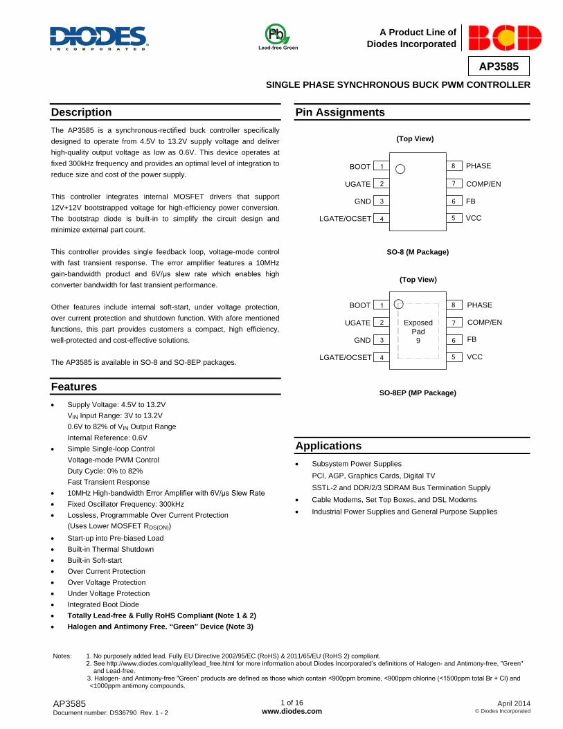
Pin Assignments
(Top View)
SO-8 (M Package)
(Top View)
SO-8EP (MP Package)
Applications
Subsystem Power Supplies
PCI, AGP, Graphics Cards, Digital TV
SSTL-2 and DDR/2/3 SDRAM Bus Termination Supply
Cable Modems, Set Top Boxes, and DSL Modems
Industrial Power Supplies and General Purpose Supplies
Notes: 1. No purposely added lead. Fully EU Directive 2002/95/EC (RoHS) & 2011/65/EU (RoHS 2) compliant. 2. See http://www.diodes.com/quality/lead_free.html for more information about Diodes Incorporated’s definitions of Halogen- and Antimony-free, "Green" and Lead-free. 3. Halogen- and Antimony-free "Green” products are defined as those which contain <900ppm bromine, <900ppm chlorine (<1500ppm total Br + Cl) and <1000ppm antimony compounds.
1
2
3
4
8
7
6
5
BOOT
UGATE
GND
PHASE
COMP/EN
FB
VCCLGATE/OCSET
1
2
3
4
8
7
6
5
BOOT
UGATE
GND
LGATE/OCSET
PHASE
COMP/EN
FB
VCC
Exposed
Pad
9
Page 2
AP3585 Document number: DS36790 Rev. 1 - 2
2 of 16 www.diodes.com
April 2014 © Diodes Incorporated
AP3585
A Product Line of
Diodes Incorporated
Typical Applications Circuit
VCC
COMP
/EN
FBGND
LGATE
/OCSET
PHASE
UGATE
BOOT1
2
3
4
5
6
7
8ON
OFF
Q3
2N7002
C2
15pF
C5 1mF
C1
10nF
R3
10kW
C4
0.1mF
Q2
NTD4965
Q1NTD4963
L1 1mH
ROCSET
COUT
1000mFX 2
VOUT
CIN1
10mF
CIN2
270mF
VIN
R5
2R2
VCC Supply
(5V to 12V)
R1 1kWR2
2kW
AP3585
Pin Descriptions
Pin Number Pin Name Function
SO-8 SO-8EP
1 1 BOOT Bootstrap pin. Connect a bootstrap capacitor from this pin to PHASE for creating a BOOT voltage suitable to drive a standard N-Channel MOSFET
2 2 UGATE Upper-gate drive pin. Connect this pin to the upper MOSFET gate providing the gate drive. This pin is monitored by the adaptive shoot-through protection circuitry to determine when the upper MOSFET has turned off
3 3 GND
Ground for the IC. All voltage levels are measured with respect to this pin. Connect this pin directly to the low side MOSFET source and ground plane with the lowest impedance. The exposed pad must be soldered to a large PCB and connected to GND for maximum power dissipation
4 4 LGATE/OCSET Low-side Gate Driver Output and Over-Current Setting Input. This pin is the gate driver for low-side MOSFET. It is also used to set the maximum inductor current. Refer to the section in “Function Description” for detail
5 5 VCC Bias supply pin. Provides a 4.5V to 13.2V bias supply for the chip from this pin. The pin should be bypassed with a capacitor to GND
6 6 FB
Feedback pin. This pin is the inverting input of the internal error amplifier. Use FB pin, in combination with the COMP pin, to compensate the voltage control feedback loop of the converter. A resistor divider from output to GND is used to set the output voltage
7 7 COMP/EN Compensation and disable pin. This pin is the output of the Error Amplifier. Pull COMP pin low will shut down the IC
8 8 PHASE This pin connects to the source of the upper MOSFET and the drain of the lower MOSFET. This pin is also monitored by the adaptive shoot-through protection circuitry to determine when the upper MOSFET has turned off
– 9 Exposed Pad Exposed Pad as ground pin
Page 3
AP3585 Document number: DS36790 Rev. 1 - 2
3 of 16 www.diodes.com
April 2014 © Diodes Incorporated
AP3585
A Product Line of
Diodes Incorporated
Functional Block Diagram
VREF 0.6V0.3V
Error Amplifier
OVP
Comparator
UVP
Comparator
VCC
GND
LGATE/
OCSET
PHASE
UGATE
BOOT
VCC
Sense Low Side
inhibit
2*VROCSET
PWM
Comparator
Disable
COMP/ENFB
+
-
+
-
+
-
+
-
-
+
+
+
-
0.4
0.8
Oscillator
Gate
Control
IZCMP+
-
Power-On-Reset
Soft-Start
And
Fault Logic
Sample
And
HoldRegulator
To LGATE
VREF
(0.6V Typ)
3V
IOCSET
(21.5mA typ)
VROCSET
Soft Start
5
1
2
8
4
376
Page 4
AP3585 Document number: DS36790 Rev. 1 - 2
4 of 16 www.diodes.com
April 2014 © Diodes Incorporated
AP3585
A Product Line of
Diodes Incorporated
Absolute Maximum Ratings (Note 4)
Symbol Parameter Rating Unit
VCC Supply Input Voltage -0.3 to 15 V
VBOOT-PHASE BOOT to PHASE Voltage -0.3 to 15 V
VUGATE UGATE to PHASE Voltage DC -0.3 to VBOOT-PHASE+0.3
V <200ns -5 to VBOOT-PHASE+5
VPHASE PHASE to GND Voltage DC -0.3 to 15
V <200ns -5 to 30
VLGATE LGATE to GND Voltage DC -0.3 to VCC+0.3
V <200ns -5 to VCC+5
– Other Pin Voltage -0.3 to 6 V
PD Power Dissipation SO-8 0.87
W SO-8EP 1.43
θJA Thermal Resistance (Junction to Ambient) SO-8 115
ºC/W SO-8EP 70
θJC Thermal Resistance (Junction to Case) SO-8 22
ºC/W SO-8EP 22
TJ Operating Junction Temperature -40 to +125 ºC
TSTG Storage Temperature -65 to +150 ºC
TLEAD Lead Temperature (Soldering, 10 sec) +260 ºC
– ESD (Human Body Model) (Note 5) 2000 V
– ESD (Machine Model) (Note 5) 200 V
Notes: 4. Stresses greater than those listed under “Absolute Maximum Ratings” may cause permanent damage to the device. These are stress ratings only, and functional operation of the device at these or any other conditions beyond those indicated under “Recommended Operating Conditions” is not implied. Exposure to “Absolute Maximum Ratings” for extended periods may affect device reliability.
5. Devices are ESD sensitive. Handling precaution is recommended.
Recommended Operating Conditions
Symbol Parameter Min Max Unit
VCC Supply Input Voltage 4.5 13.2 V
TA Operating Ambient Temperature -40 +85 C
Page 5
AP3585 Document number: DS36790 Rev. 1 - 2
5 of 16 www.diodes.com
April 2014 © Diodes Incorporated
AP3585
A Product Line of
Diodes Incorporated
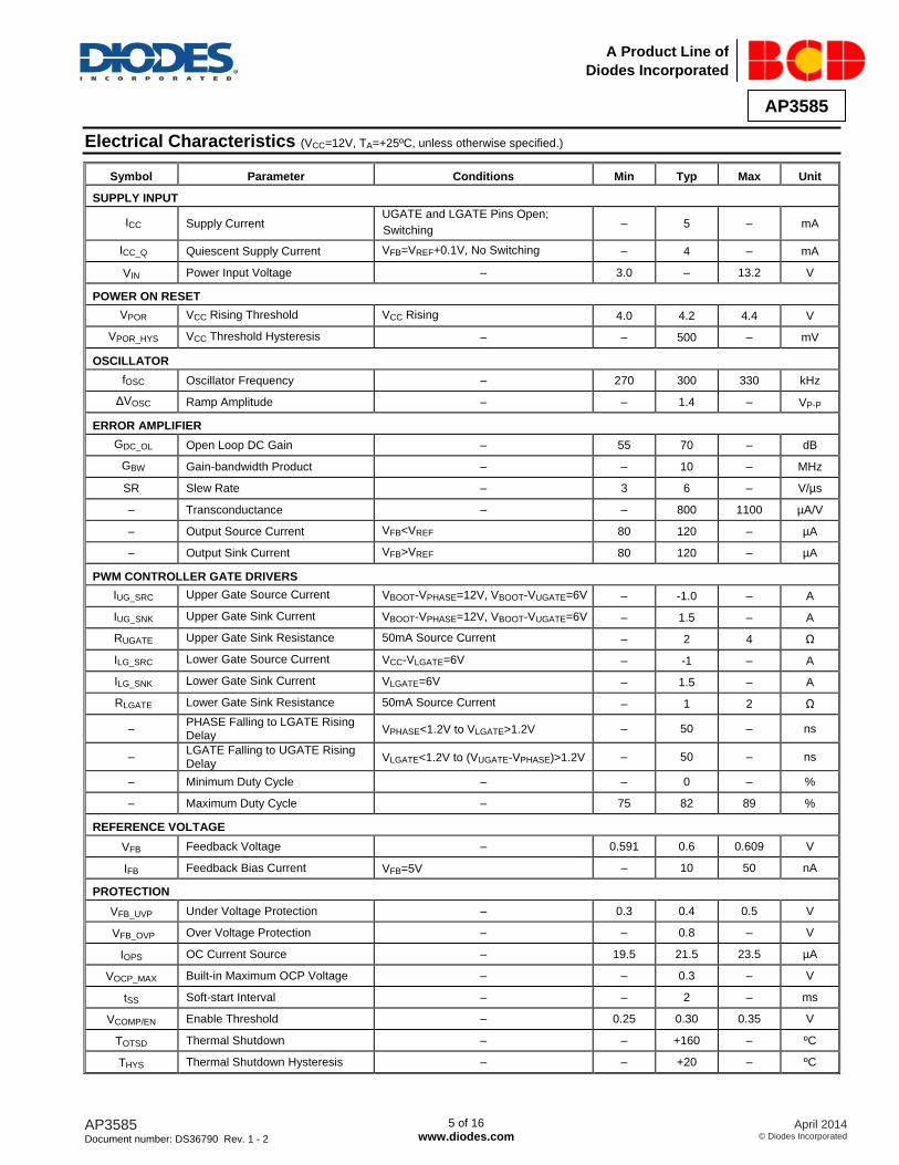
Electrical Characteristics (VCC=12V, TA=+25ºC, unless otherwise specified.)
Symbol Parameter Conditions Min Typ Max Unit
SUPPLY INPUT
ICC Supply Current UGATE and LGATE Pins Open;
Switching – 5 – mA
ICC_Q Quiescent Supply Current VFB=VREF+0.1V, No Switching – 4 – mA
VIN Power Input Voltage – 3.0 – 13.2 V
POWER ON RESET
VPOR VCC Rising Threshold VCC Rising 4.0 4.2 4.4 V
VPOR_HYS VCC Threshold Hysteresis – – 500 – mV
OSCILLATOR
fOSC Oscillator Frequency – 270 300 330 kHz
ΔVOSC Ramp Amplitude – – 1.4 – VP-P
ERROR AMPLIFIER
GDC_OL Open Loop DC Gain – 55 70 – dB
GBW Gain-bandwidth Product – – 10 – MHz
SR Slew Rate – 3 6 – V/µs
– Transconductance – – 800 1100 µA/V
– Output Source Current VFB<VREF 80 120 – µA
– Output Sink Current VFB>VREF 80 120 – µA
PWM CONTROLLER GATE DRIVERS
IUG_SRC Upper Gate Source Current VBOOT-VPHASE=12V, VBOOT-VUGATE=6V – -1.0 – A
IUG_SNK Upper Gate Sink Current VBOOT-VPHASE=12V, VBOOT-VUGATE=6V – 1.5 – A
RUGATE Upper Gate Sink Resistance 50mA Source Current – 2 4 Ω
ILG_SRC Lower Gate Source Current VCC-VLGATE=6V – -1 – A
ILG_SNK Lower Gate Sink Current VLGATE=6V – 1.5 – A
RLGATE Lower Gate Sink Resistance 50mA Source Current – 1 2 Ω
– PHASE Falling to LGATE Rising Delay
VPHASE<1.2V to VLGATE>1.2V – 50 – ns
– LGATE Falling to UGATE Rising Delay
VLGATE<1.2V to (VUGATE-VPHASE)>1.2V – 50 – ns
– Minimum Duty Cycle – – 0 – %
– Maximum Duty Cycle – 75 82 89 %
REFERENCE VOLTAGE
VFB Feedback Voltage – 0.591 0.6 0.609 V
IFB Feedback Bias Current VFB=5V – 10 50 nA
PROTECTION
VFB_UVP Under Voltage Protection – 0.3 0.4 0.5 V
VFB_OVP Over Voltage Protection – – 0.8 – V
IOPS OC Current Source – 19.5 21.5 23.5 µA
VOCP_MAX Built-in Maximum OCP Voltage – – 0.3 – V
tSS Soft-start Interval – – 2 – ms
VCOMP/EN Enable Threshold – 0.25 0.30 0.35 V
TOTSD Thermal Shutdown – – +160 – ºC
THYS Thermal Shutdown Hysteresis – – +20 – ºC
Page 6
AP3585 Document number: DS36790 Rev. 1 - 2
6 of 16 www.diodes.com
April 2014 © Diodes Incorporated
AP3585
A Product Line of
Diodes Incorporated
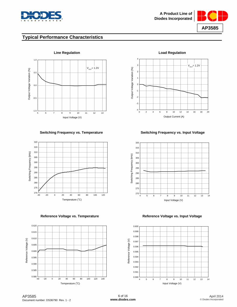
Typical Performance Characteristics
Line Regulation Load Regulation
Switching Frequency vs. Temperature Switching Frequency vs. Input Voltage
Reference Voltage vs. Temperature Reference Voltage vs. Input Voltage
5 6 7 8 9 10 11 12 13-1.0
-0.5
0.0
0.5
1.0
Ou
tpu
t V
olta
ge
Va
ria
tio
n (
%)
Input Voltage (V)
VOUT
= 1.2V
0 2 4 6 8 10 12 14 16 18 20-4
-3
-2
-1
0
1
2
3
4
Ou
tpu
t V
olta
ge
Va
ria
tio
n (
%)
Output Current (A)
VOUT
= 1.2V
-40 -20 0 20 40 60 80 100 120270
275
280
285
290
295
300
305
310
315
320
Sw
itch
ing
Fre
qu
en
cy (
kH
z)
Temperature (oC)
4 5 6 7 8 9 10 11 12 13 14270
275
280
285
290
295
300
305
310
315
320
Sw
itch
ing
Fre
qu
en
cy (
kH
z)
Input Voltage (V)
-40 -20 0 20 40 60 80 100 120 1400.580
0.585
0.590
0.595
0.600
0.605
0.610
0.615
0.620
Re
fere
nce
Vo
lta
ge
(V
)
Temperature (oC)
4 5 6 7 8 9 10 11 12 13 140.590
0.591
0.592
0.593
0.594
0.595
0.596
0.597
0.598
0.599
0.600
Re
fere
nce
Vo
lta
ge
(V
)
Input Voltage (V)
Page 7
AP3585 Document number: DS36790 Rev. 1 - 2
7 of 16 www.diodes.com
April 2014 © Diodes Incorporated
AP3585
A Product Line of
Diodes Incorporated
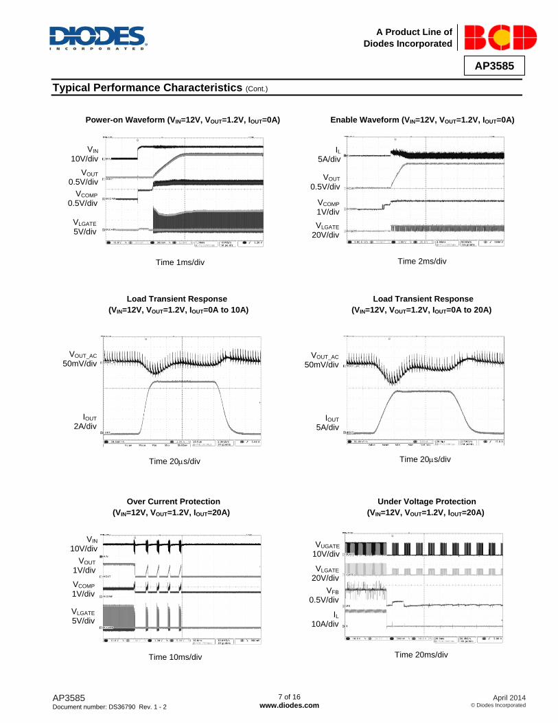
Typical Performance Characteristics (Cont.)
Power-on Waveform (VIN=12V, VOUT=1.2V, IOUT=0A) Enable Waveform (VIN=12V, VOUT=1.2V, IOUT=0A)
Load Transient Response Load Transient Response
(VIN=12V, VOUT=1.2V, IOUT=0A to 10A) (VIN=12V, VOUT=1.2V, IOUT=0A to 20A)
Over Current Protection Under Voltage Protection
(VIN=12V, VOUT=1.2V, IOUT=20A) (VIN=12V, VOUT=1.2V, IOUT=20A)
VIN 10V/div
VOUT 0.5V/div
Time 1ms/div
IL 5A/div
VCOMP 0.5V/div
VLGATE 5V/div
VOUT 0.5V/div
VCOMP 1V/div
VLGATE 20V/div
Time 2ms/div
VOUT_AC 50mV/div
IOUT 2A/div
Time 20ms/div
VOUT_AC 50mV/div
IOUT 5A/div
Time 20ms/div
VIN 10V/div
VUGATE 10V/div
VOUT 1V/div
VCOMP 1V/div
VLGATE 5V/div
Time 10ms/div
VLGATE 20V/div
VFB 0.5V/div
IL 10A/div
Time 20ms/div
Page 8
AP3585 Document number: DS36790 Rev. 1 - 2
8 of 16 www.diodes.com
April 2014 © Diodes Incorporated
AP3585
A Product Line of
Diodes Incorporated
Functional Descriptions
The AP3585 is a voltage-mode single phase synchronous buck controller with embedded MOSFET drivers. This part provides complete protection
functions such as over voltage protection, under voltage protection and over current protection. Inductor current information is sensed by RDS(ON)
of the low side MOSFET. The over current protection threshold can be simply programmed by a resistor.
Power on Reset and Chip Enable
A power on reset (POR) circuitry continuously monitors the supply voltage at VCC pin. Once the rising POR threshold is exceeded, the AP3585
sets itself to active state and is ready to accept chip enable command. The rising POR threshold is typically 4.2V at VCC rising.
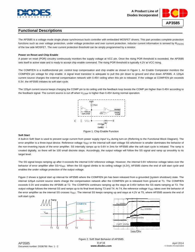
The COMP/EN is a multifunctional pin: control loop compensation and chip enable as shown in Figure 1. An Enable Comparator monitors the
COMP/EN pin voltage for chip enable. A signal level transistor is adequate to pull this pin down to ground and shut down AP3585. A 120µA
current source charges the external compensation network with 0.45V ceiling when this pin is released. If the voltage at COMP/EN pin exceeds
0.3V, the AP3585 initiates its soft start cycle.
The 120µA current source keeps charging the COMP pin to its ceiling until the feedback loop boosts the COMP pin higher than 0.45V according to
the feedback signal. The current source is cut off when VCOMP is higher than 0.45V during normal operation.
Figure 1. Chip Enable Function
Soft Start
A built-in Soft Start is used to prevent surge current from power supply input VIN during turn-on (Referring to the Functional Block Diagram). The
error amplifier is a three-input device. Reference voltage VREF or the internal soft start voltage SS whichever is smaller dominates the behavior of
the non-inverting inputs of the error amplifier. SS internally ramps up to 0.6V in 2ms for AP3585 after the soft start cycle is initiated. The ramp is
created digitally, so there will be 100 small discrete steps. Accordingly, the output voltage will follow the SS signal and ramp up smoothly to its
target level.
The SS signal keeps ramping up after it exceeds the internal 0.6V reference voltage. However, the internal 0.6V reference voltage takes over the
behavior of error amplifier after SS>VREF. When the SS signal climbs to its ceiling voltage (4.2V), AP3585 claims the end of soft start cycle and
enables the under voltage protection of the output voltage.
Figure 2 shows a typical start up interval for AP3585 where the COMP/EN pin has been released from a grounded (system shutdown) state. The
internal 120µA current source starts charge the compensation network after the COMP/EN pin is released from ground at T1. The COMP/EN
exceeds 0.3V and enables the AP3585 at T2. The COMP/EN continues ramping up the stays at 0.45V before the SS starts ramping at T3. The
output voltage follows the internal SS and ramps up to its final level during T3 and T4. At T4, the reference voltage VREF takes over the behavior of
the error amplifier as the internal SS crosses VREF. The internal SS keeps ramping up and stays at 4.2V at T5, where AP3585 asserts the end of
soft start cycle.
VIN 10V/Div
VOUT 0.5V/Div
COMP 0.5V/Div
LGATE 10V/Div
1ms/Div
Figure 2. Soft Start Behavior of AP3585
Page 9
AP3585 Document number: DS36790 Rev. 1 - 2
9 of 16 www.diodes.com
April 2014 © Diodes Incorporated
AP3585
A Product Line of
Diodes Incorporated
Functional Descriptions (Cont.)
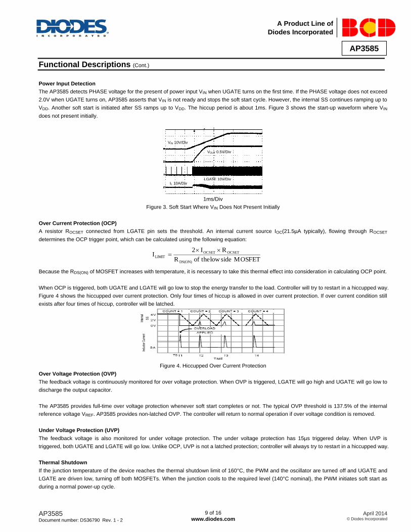
Power Input Detection
The AP3585 detects PHASE voltage for the present of power input VIN when UGATE turns on the first time. If the PHASE voltage does not exceed
2.0V when UGATE turns on, AP3585 asserts that VIN is not ready and stops the soft start cycle. However, the internal SS continues ramping up to
VDD. Another soft start is initiated after SS ramps up to VDD. The hiccup period is about 1ms. Figure 3 shows the start-up waveform where VIN
does not present initially.
VIN 10V/Div
VOUT 0.5V/Div
IL 10A/Div LGATE 10V/Div
1ms/Div
Figure 3. Soft Start Where VIN Does Not Present Initially
Over Current Protection (OCP)
A resistor ROCSET connected from LGATE pin sets the threshold. An internal current source IOC(21.5µA typically), flowing through ROCSET
determines the OCP trigger point, which can be calculated using the following equation:
Because the RDS(ON) of MOSFET increases with temperature, it is necessary to take this thermal effect into consideration in calculating OCP point.
When OCP is triggered, both UGATE and LGATE will go low to stop the energy transfer to the load. Controller will try to restart in a hiccupped way.
Figure 4 shows the hiccupped over current protection. Only four times of hiccup is allowed in over current protection. If over current condition still
exists after four times of hiccup, controller will be latched.
Figure 4. Hiccupped Over Current Protection
Over Voltage Protection (OVP)
The feedback voltage is continuously monitored for over voltage protection. When OVP is triggered, LGATE will go high and UGATE will go low to
discharge the output capacitor.
The AP3585 provides full-time over voltage protection whenever soft start completes or not. The typical OVP threshold is 137.5% of the internal
reference voltage VREF. AP3585 provides non-latched OVP. The controller will return to normal operation if over voltage condition is removed.
Under Voltage Protection (UVP)
The feedback voltage is also monitored for under voltage protection. The under voltage protection has 15µs triggered delay. When UVP is
triggered, both UGATE and LGATE will go low. Unlike OCP, UVP is not a latched protection; controller will always try to restart in a hiccupped way.
Thermal Shutdown
If the junction temperature of the device reaches the thermal shutdown limit of 160°C, the PWM and the oscillator are turned off and UGATE and
LGATE are driven low, turning off both MOSFETs. When the junction cools to the required level (140°C nominal), the PWM initiates soft start as
during a normal power-up cycle.
MOSFET sidelowtheofR
R I 2I
DS(ON)
OCSETOCSET
LIMIT
Page 10
AP3585 Document number: DS36790 Rev. 1 - 2
10 of 16 www.diodes.com
April 2014 © Diodes Incorporated
AP3585
A Product Line of
Diodes Incorporated
Functional Descriptions (Cont.)
Output Voltage Selection
The output voltage can be programmed to any level between the 0.6V internal reference to the 82% of VIN supply. The lower limitation of output
voltage is caused by the internal reference. The upper limitation of the output voltage is caused by the maximum available duty cycle (82%). This
is to leave enough time for over-current detection. Output voltage out of this range is not allowed.
A voltage divider sets the output voltage (Refer to the typical application circuit). In real applications, choose R1 in 100Ω to 10kΩ range and
choose appropriate R2 according to the desired output voltage.
PCB Layout Considerations
High speed switching and relatively large peak currents in a synchronous-rectified buck converter make the PCB layout a very important part of
design. Switching current from one power device to another can generate voltage spikes across the impedances of the interconnecting bond wires
and circuit traces. The voltage spikes can degrade efficiency and radiate noise, that results in over-voltage stress on devices. Careful component
placement layout a printed circuit design can minimize the voltage spikes induced in the converter.
Follow the below layout guidelines for optimal performance of AP3585.
1. The turn-off transition of the upper MOSFET prior to turn-off, the upper MOSFET was carrying the full load current. During turn-off, current stops
flowing in the upper MOSFET and is picked up by the low side MOSFET. Any inductance in the switched path generates a large voltage spike
during the switching interval. Careful component selections, layout of the critical components, and use shorter and wider PCB traces help in
minimizing the magnitude of voltage spikes.
2. The power components and the PWM controller should be placed firstly. Place the input capacitors, especially the high-frequency ceramic
decoupling capacitors, close to the power switches. Place the output inductor and output capacitors between the MOSFETs and the load. Also
locate the PWM controller near MOSFETs.
3. Use a dedicated grounding plane and use vias to ground all critical components to this layer. Use an immediate via to connect the component to
ground plane including GND of AP3585.
4. Apply another solid layer as a power plane and cut this plane into smaller islands of common voltage levels. The power plane should support
the input power and output power nodes. Use copper filled polygons on the top and bottom circuit layers for the PHASE node.
5. The PHASE node is subject to very high dV/dt voltages. Stray capacitance between this island and the surrounding circuitry tend to induce
current spike and capacitive noise coupling. Keep the sensitive circuit away from the PHASE node and keep the PCB area small to limit the
capacitive coupling. However, the PCB area should be kept moderate since it also acts as main heat convection path of the lower MOSFET.
6. The PCB traces between the PWM controller and the gate of MOSFET and also the traces connecting source of MOSFETs should be sized to
carry 2A peak currents.
R2
R2R10.6VVOUT
Page 11
AP3585 Document number: DS36790 Rev. 1 - 2
11 of 16 www.diodes.com
April 2014 © Diodes Incorporated
AP3585
A Product Line of
Diodes Incorporated
Ordering Information
AP3585 XX XX - XX
PackingPackage
TR : Tape & ReelM: SO-8
MP: SO-8EPG1 : Green
Product Name RoHS/Green
Diodes IC’s Pb-free products with "G1" suffix in the part number, are RoHS compliant and green.
Package Temperature Range Part Number Marking ID Packing
SO-8 -40°C to +85°C
AP3585MTR-G1 3585M-G1 4000/Tape & Reel
SO-8EP AP3585MPTR-G1 3585MP-G1 4000/Tape & Reel
Marking Information
First and Second Lines: Logo and Marking ID Third Line: Date Code Y: Year WW: Work Week of Molding M: Assembly House Code XX: 7
th and 8
th Digits of Batch No.
Page 12
AP3585 Document number: DS36790 Rev. 1 - 2
12 of 16 www.diodes.com
April 2014 © Diodes Incorporated
AP3585
A Product Line of
Diodes Incorporated
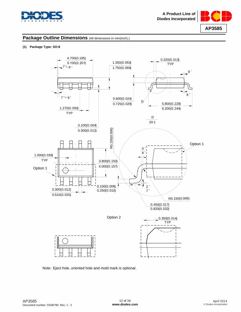
Package Outline Dimensions (All dimensions in mm(inch).)
(1) Package Type: SO-8
0°
8°
1°
7°
R0.150(0.006)
R0.1
50(0
.006)
1.000(0.039)
0.300(0.012)
0.510(0.020)
1.350(0.053)
1.750(0.069)
0.100(0.004)
0.300(0.012)
3.800(0.150)
4.000(0.157)
7°
7°
20:1
D
1.270(0.050)
TYP
0.150(0.006)
0.250(0.010)
8°
D5.800(0.228)
6.200(0.244)
0.600(0.024)
0.725(0.029)
0.320(0.013)
8°
0.450(0.017)
0.820(0.032)
4.700(0.185)
5.100(0.201)
Note: Eject hole , oriented hole and mold mark is optional.
Option 1
Option 1
Option 2 0.350(0.014)
TYP
TYP
TYP9°~
9°~
Page 13
AP3585 Document number: DS36790 Rev. 1 - 2
13 of 16 www.diodes.com
April 2014 © Diodes Incorporated
AP3585
A Product Line of
Diodes Incorporated
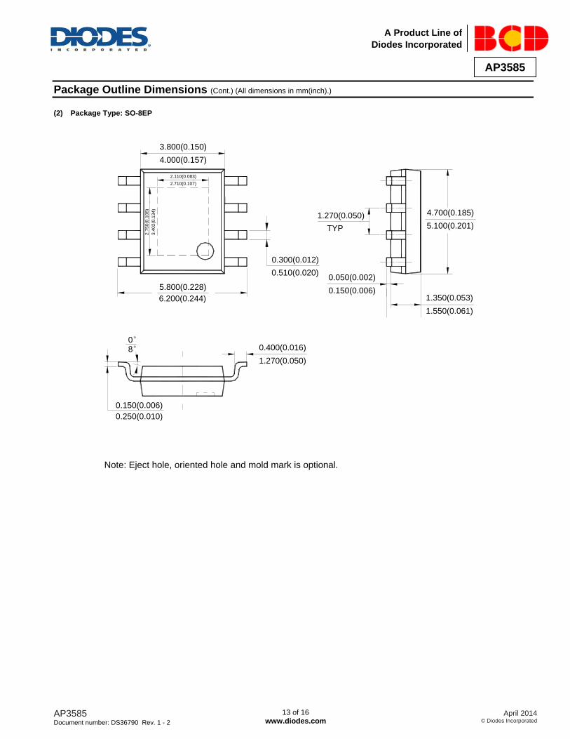
Package Outline Dimensions (Cont.) (All dimensions in mm(inch).)
(2) Package Type: SO-8EP
8°
5.800(0.228)
6.200(0.244)
1.270(0.050)
0.400(0.016)
3.800(0.150)
4.000(0.157)
0.510(0.020)0.050(0.002)
0.150(0.006)
4.700(0.185)1.270(0.050)
TYP
0°
0.250(0.010)
0.150(0.006)
1.350(0.053)
1.550(0.061)
2.110(0.083)
2.710(0.107)
2.7
50(0
.10
8)
3.4
02(0
.13
4)
5.100(0.201)
Note: Eject hole, oriented hole and mold mark is optional.
0.300(0.012)
Page 14
AP3585 Document number: DS36790 Rev. 1 - 2
14 of 16 www.diodes.com
April 2014 © Diodes Incorporated
AP3585
A Product Line of
Diodes Incorporated
Suggested Pad Layout
(1) Package Type: SO-8
Grid
placement
courtyard
ZG
Y
E X
Dimensions Z
(mm)/(inch) G
(mm)/(inch) X
(mm)/(inch) Y
(mm)/(inch) E
(mm)/(inch)
Value 6.900/0.272 3.900/0.154 0.650/0.026 1.500/0.059 1.270/0.050
Page 15
AP3585 Document number: DS36790 Rev. 1 - 2
15 of 16 www.diodes.com
April 2014 © Diodes Incorporated
AP3585
A Product Line of
Diodes Incorporated
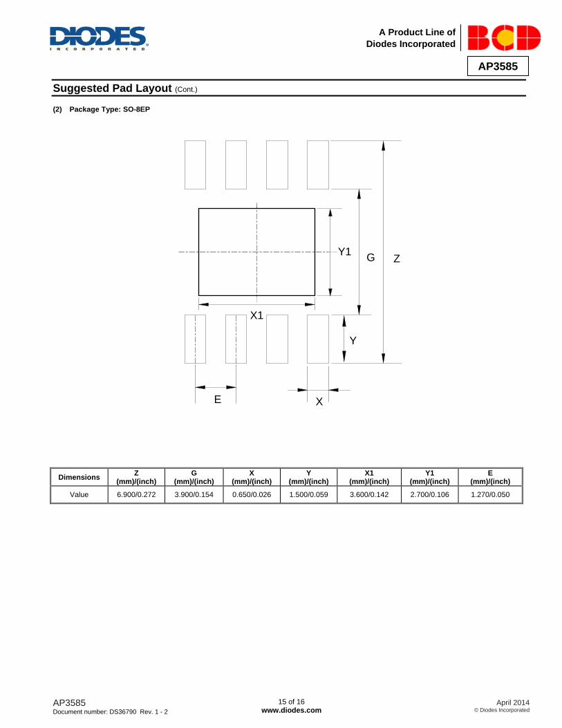
Suggested Pad Layout (Cont.)
(2) Package Type: SO-8EP
G
E X
X1
Y
Y1Z
Dimensions Z
(mm)/(inch) G
(mm)/(inch) X
(mm)/(inch) Y
(mm)/(inch) X1
(mm)/(inch) Y1
(mm)/(inch) E
(mm)/(inch)
Value 6.900/0.272 3.900/0.154 0.650/0.026 1.500/0.059 3.600/0.142 2.700/0.106 1.270/0.050
Page 16
AP3585 Document number: DS36790 Rev. 1 - 2
16 of 16 www.diodes.com
April 2014 © Diodes Incorporated
AP3585
A Product Line of
Diodes Incorporated
IMPORTANT NOTICE DIODES INCORPORATED MAKES NO WARRANTY OF ANY KIND, EXPRESS OR IMPLIED, WITH REGARDS TO THIS DOCUMENT, INCLUDING, BUT NOT LIMITED TO, THE IMPLIED WARRANTIES OF MERCHANTABILITY AND FITNESS FOR A PARTICULAR PURPOSE (AND THEIR EQUIVALENTS UNDER THE LAWS OF ANY JURISDICTION). Diodes Incorporated and its subsidiaries reserve the right to make modifications, enhancements, improvements, corrections or other changes without further notice to this document and any product described herein. Diodes Incorporated does not assume any liability arising out of the application or use of this document or any product described herein; neither does Diodes Incorporated convey any license under its patent or trademark rights, nor the rights of others. Any Customer or user of this document or products described herein in such applications shall assume all risks of such use and will agree to hold Diodes Incorporated and all the companies whose products are represented on Diodes Incorporated website, harmless against all damages. Diodes Incorporated does not warrant or accept any liability whatsoever in respect of any products purchased through unauthorized sales channel. Should Customers purchase or use Diodes Incorporated products for any unintended or unauthorized application, Customers shall indemnify and hold Diodes Incorporated and its representatives harmless against all claims, damages, expenses, and attorney fees arising out of, directly or indirectly, any claim of personal injury or death associated with such unintended or unauthorized application. Products described herein may be covered by one or more United States, international or foreign patents pending. Product names and markings noted herein may also be covered by one or more United States, international or foreign trademarks. This document is written in English but may be translated into multiple languages for reference. Only the English version of this document is the final and determinative format released by Diodes Incorporated.
LIFE SUPPORT Diodes Incorporated products are specifically not authorized for use as critical components in life support devices or systems without the express written approval of the Chief Executive Officer of Diodes Incorporated. As used herein: A. Life support devices or systems are devices or systems which: 1. are intended to implant into the body, or
2. support or sustain life and whose failure to perform when properly used in accordance with instructions for use provided in the labeling can be reasonably expected to result in significant injury to the user.
B. A critical component is any component in a life support device or system whose failure to perform can be reasonably expected to cause the failure of the life support device or to affect its safety or effectiveness. Customers represent that they have all necessary expertise in the safety and regulatory ramifications of their life support devices or systems, and acknowledge and agree that they are solely responsible for all legal, regulatory and safety-related requirements concerning their products and any use of Diodes Incorporated products in such safety-critical, life support devices or systems, notwithstanding any devices- or systems-related information or support that may be provided by Diodes Incorporated. Further, Customers must fully indemnify Diodes Incorporated and its representatives against any damages arising out of the use of Diodes Incorporated products in such safety-critical, life support devices or systems. Copyright © 2012, Diodes Incorporated www.diodes.com