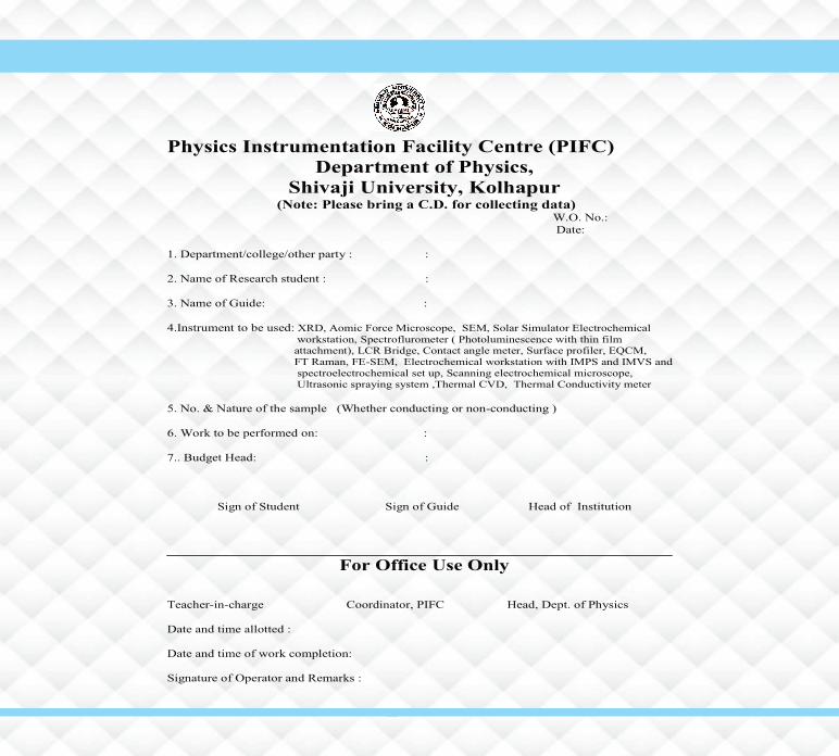
SHIVAJI UNIVERSITY KOLHAPUR DEPARTMENT OF HYSICS P Physics Instrumental Facility Center (PIFC) Facili available ties Scanning Electron Microscope (SEM) with EDS Field Emission Scanning Electron Microscope with EDS X- Ray Diffractometer (XRD) Atomic Force Microscope FT-IR Spectrometer Spectroscopic Ellipsometer LCR Meter Bridge Electrochemical Impedance Spectrometer (EIS) FT-RAMAN spectrometer Contact angle meter Surface area analyzer (BET) Solar Simulator Electrochemical Quartz Crystal Microbalance (EQCM) Scanning electrochemical microscope (SECM) IMPS/ IMVS (In situ Spectroelectrochemistry) Electrochemical workstation Spectroluorometer (PL) Surface Proiler Uv-Vis Spectrophotometer Electrometer
Transcript
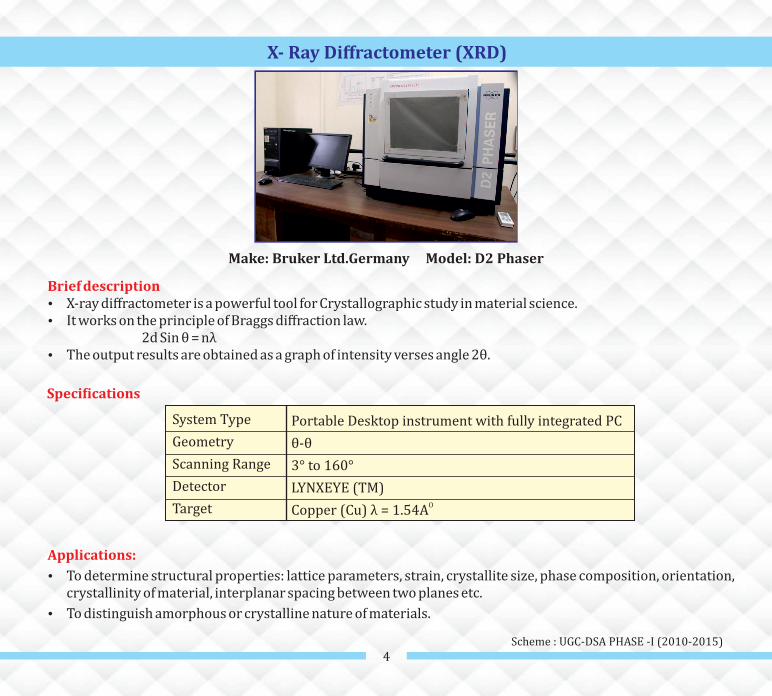
SHIVAJIUNIVERSITY KOLHAPUR
DEPARTMENT OF HYSICSPPhysics Instrumental Facility Center (PIFC)
Facili availableties
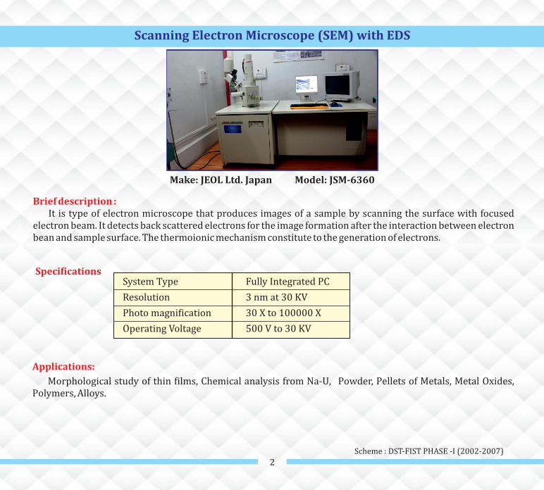
Scanning Electron Microscope (SEM) with EDS
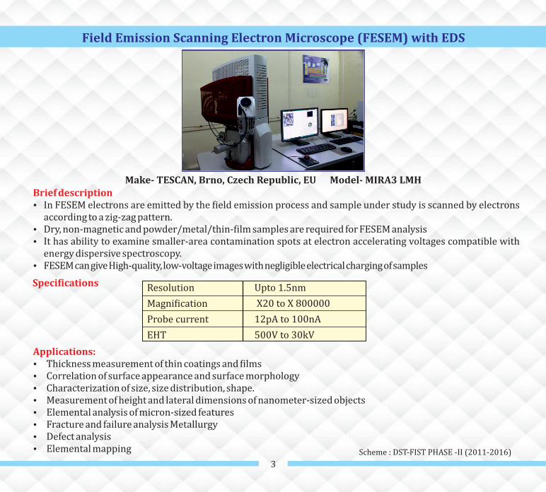
Field Emission Scanning Electron Microscope with EDS
crystallinity of material, interplanar spacing between two planes etc.
Applications:
� To distinguish amorphous or crystalline nature of materials.
System Type
Geometry
Scanning Range
Detector
Target
Portable Desktop instrument with fully integrated PC
θ-θ
3° to 160°
LYNXEYE (TM)
Copper (Cu) = 1.54Aλ O
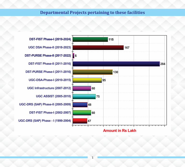
Scheme : UGC-DSA PHASE -I (2010-2015)
5
Atomic Force Microscope (AFM)
Scheme : UGC-DSA Phase-I (2010-15)
Make: USA Model: INOVVA 1B3BE
� AFM microscopes operate on the principle of surface sensing using an extremely sharp tip on a micromachined
silicon probe.
� Innova Atomic Force Microscope (AFM) delivers accurate, high-resolution imaging and a wide range of
functionality for advanced research in physical, life, and material sciences.
� It offers a unique, state-of-the-art closed-loop scan linearization system that ensures accurate measurements
and noise levels approaching those of open-loop operation.
Brief description
Applications:
� To determine the particle size and roughness of the sample in material science
� To capture 2D and 3D images of the surface
� In the !ield of stem cell and tissue engineering
Operating Mode
XY Scan Range
Z Scan Range
(1) Contact mode (2)Tapping Mode
1-90 µm
50 nm-7.5 µm
Speci!ications
6
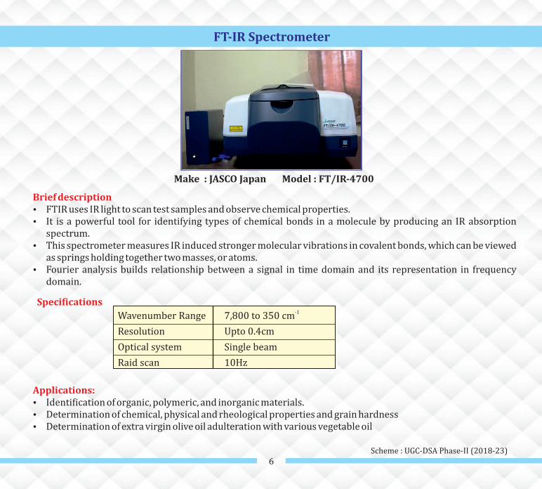
Make : JASCO Japan Model : FT/IR-4700
� It is a powerful tool for identifying types of chemical bonds in a molecule by producing an absorption
spectrum
IR
.
Brief description
� FTIR uses light to scan test samples and observe chemical properties.IR
� Fourier analysis builds relationship between a signal in time domain and its representation in frequency
domain.
� This spectrometer measures IR induced stronger molecular vibrations in covalent bonds, which can be viewed
as springs holding together two masses, or atoms.
� Dete mination chemical, physical and rheological properties and grain hardnessr of
Applications:
� Determination of extra virgin olive oil adulteration with various vegetable oil
� Identi!ication of organic, polymeric, and inorganic materials.
Speci!ications
Wave ange
Resolution
Optical system
Raid scan
number R 7,800 to 350 cm
Upto 0.4cm
Single beam
10Hz
-1
FT-IR Spectrometer
Scheme : UGC-DSA Phase- I (201 )I 8-23
7
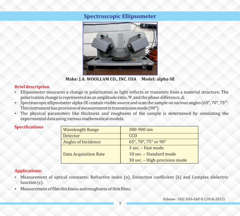
Spectroscopic Ellipsometer
Scheme : UGC-DSA-SAP-II (2018-2023)
Make: J.A. WOOLLAM CO., INC. USA Model: alpha-SE
� Ellipsometer measures a change in polarization as light re!lects or transmits from a material structure. The
polarization change is represented as an amplitude ratio, Ψ, and the phase difference, Δ.
Brief description
� Spectroscopic ellipsometer alpha-SE contain visible source and scan the sample on various angles (65 , 70 , 75
This instrument hasprovision ofmeasurement in transmission mode(90 )
# # #⁾.# .
� The physical parameters like thickness and roughness of the sample is determined by simulating the
experimental data using various mathematical models.
Speci!ications
Applications:
� Measurement of %ilm thickness and roughness of thin %ilms.
� Measurement of optical constants: Refractive index (n), Extinction coef!icient (k) and Complex dielectric
function (ε).
Wavelength Range
Detector
Angles of Incidence
Data Acquisition Rate
380-900 nm
CCD
65°, 70°, 75° or 90°
3 sec. – Fast mode
10 sec. – Standard mode
30 sec. – High-precision mode
8
Make: Hewlett Packard (HP) Model: 4284A
� It is basically inductance L , capacitance C, and resistance R measuring device.
� LCR Meter for electrical properties measurement with respect to frequencies are based on Auto balancing
bridge method.
Brief description
� LCR Meters are generally used for easy and accurate evaluation of components like capacitors, inductors,
transformers and electromechanical devices.
LCR Meter Bridge
Scheme : UGC-DRS PHASE-I (1999-2004)
:Applications
� Power inductor characterizations
� Semiconductor C-V evaluation
� Determination of Dielectric Constant
Frequency Range
Impedance Range
Measurement Terminals
Accuracy Z
D
Output Impedance
Measurement Time
20 Hz o 2 MHz
0.01m -99.9 m
t
Ω Ω
Four-terminal pair
0.05%
0.0005
100 , ±3%
40 m sec/190 m sec/830 msec
Ω
Speci!ications
9
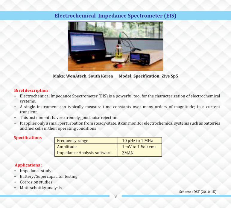
Make: WonAtech, South Korea Model: Speci!ication: Zive Sp5
Electrochemical Impedance Spectrometer (EIS)
Scheme : DST (2010-15)
� A single instrument can typically measure time constants over many orders of magnitude; in a currenttransient.
� Electrochemical Impedance Spectrometer (EIS) is a powerful tool for the characterization of electrochemicalsystems.
� This instruments have extremely good noise rejection.� It applies only a small perturbation from steady-state, it can monitor electrochemical systems such as batteries
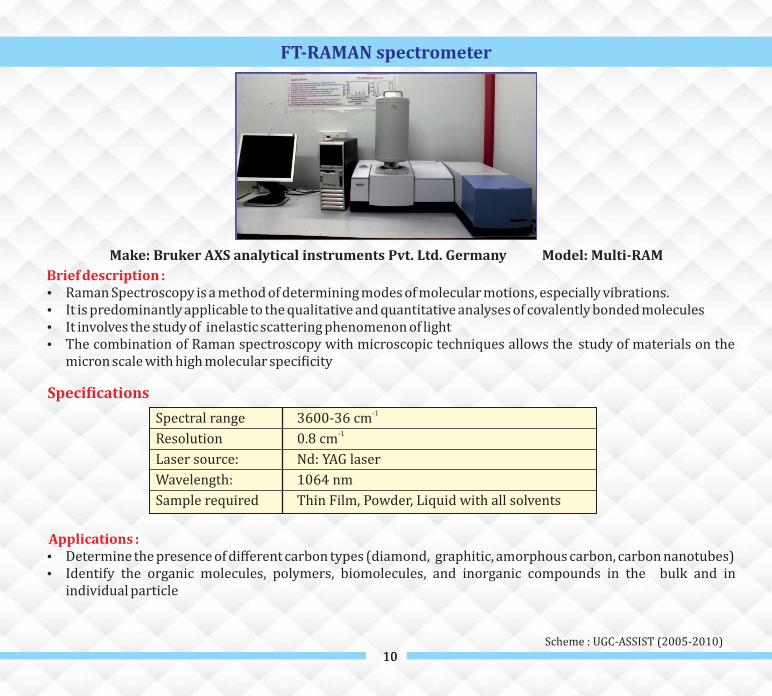
Make: Bruker AXS analytical instruments Pvt. Ltd. Germany Model: Multi-RAM
� Raman Spectroscopy is a method of determining modes of molecular motions, especially vibrations.� It is predominantly applicable to the qualitative and quantitative analyses of covalently bonded molecules
� The combination of Raman spectroscopy with microscopic techniques allows the study of materials on themicron scale with high molecular speci!icity
� It involves the study of inelastic scattering phenomenon of light
Brief description :
Applications :
� Identify the organic molecules, polymers, biomolecules, and inorganic compounds in the bulk and inindividual particle
� Determine the presence of different carbon types (diamond, graphitic, amorphous carbon, carbon nanotubes)
Speci!ications
Spectral range
Resolution
Laser source:
Wavelength:
Sample required
3600-36 cm
0.8 cm
Nd: YAG laser
1064 nm
Thin Film, Powder, Liquid with all solvents
-1
-1
10
FT-RAMAN spectrometer
Scheme : UGC-ASSIST (2005-2010)
11
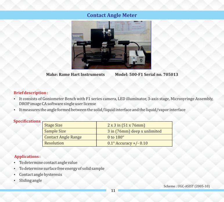
� It consists of Goniometer Bench with F1 series camera, LED illuminator, 3-axis stage, Microsyringe Assembly,DROP image CA software single user license
� It measures he angle formed between the solid/liquid interface and the liquid/vapor interfacet
Brief description :
Applications :
� To determine contact angle value
� To determine surface free energy of solid sample
� Contact angle hysteresis
� Sliding angle
Make: Rame Hart Instruments Model: 500-F1 Serial no. 705013
11
Contact Angle Meter
Scheme : UGC-ASIST (2005-10)
Speci!icationsStage Size
Sample Size
Contact Angle Range
Resolution
2 x 3 in (51 x 76mm)
3 in (76mm) deep x unlimited
0 to 180°
0.1° Accuracy +/- 0.10
12
Make: Anton paar, quanchrome instruments Mode: NOVA 1000e
� The BET theory applies to systems of multilayer adsorption and usually utilizes probing gases that do notchemically react with material surfaces (eg. N ) as adsorbates to quantify speci!ic surface area₂
� It helps to explain the physical adsorption of gas molecules on a solid surface
� Nitrogen is the most commonly employed gaseous adsorbate used for surface probing by BET methods
� It is an analysis technique for the measurement of the speci!ic surface area of materials
Brief description :
� Average pore size� Pore volume of all powder samples (~0.15 to 0.2 gm)
� Surface area
Applications :
It measures
Speci!ications
Operating temperature
Surface area range
Pore size range
Accuracy (% of span)
20-300°C
0.1 m /s to no known limit
0.35-400nm
±0.1
²
Surface Area Analyzer (BET)
Scheme : CSIR (2012-2015)
13
Make : Photo Emission Tech., Inc Model : CT 150 AAA
Brief description :
� It provides Selectable and adjustable constant intensity or constant power mode.� It includes Light intensity feedback system for stable light output intensity.
� A solar simulator (arti!icial sun) is a device that provides illumination approximating natural sunlight. Thepurpose of the solar simulator is to provide a controllable indoor test facility under laboratory conditions, usedfor the testing of solar cells, sun screen and other materials and devices.
� Determining the electric performance of the photovoltaic cells� Comparison of cell characteristics among the group of the cell� Repeated measurement of the same cell to study the life cycle
� Photovoltaic cell performanceApplications :
Max. illuminated area
Air mass
Range of light intensity
Phase/Voltage/Frequency
Power consumption
Operating working distance
6.14’’ × 6.14’’
AM0, AM1 and AM1.5
100 mW/cm 15%
Single phase/220VAC/50-60Hz
1.5 KVA
432 nm
² ,
Solar Simulator
Scheme : DST-PURSE PHASE-I (2011-2016)
Speci!ications
14
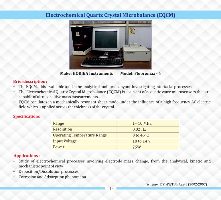
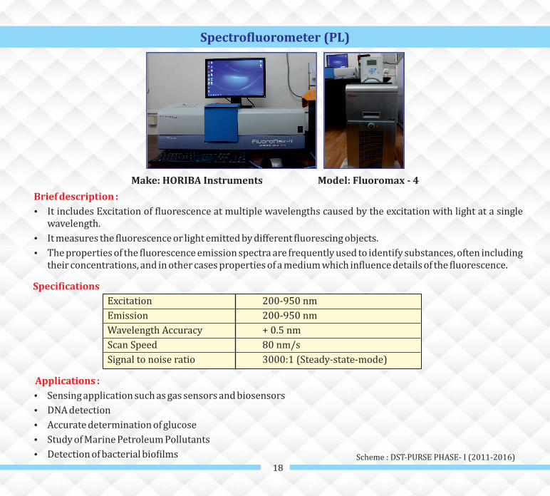
Make: HORIBA Instruments Model: Fluoromax - 4
� The Electrochemical Quartz Crystal Microbalance (EQCM) is a variant of acoustic wave microsensors that arecapable of ultrasensitive mass measurements.
Brief description :
� The EQCM adds a valuable tool in the analytical toolbox of anyone investigating interfacial processes.
� EQCM oscillates in a mechanically resonant shear mode under the in!luence of a high frequency AC electric!ield which is applied across the thickness of the crystal.
� Deposition/Dissolution processes
Applications :
� Study of electrochemical processes involving electrode mass change, from the analytical, kinetic andmechanistic point of view
Make: Metrohm Switerland Model: Autolab 302N with 32 FRA Sensolyte 0.045
Brief description :
� Scanning electrochemical microscopy (SECM) is a technique within the broader class of scanning probemicroscopy (SPM) that is used to measure the local electrochemical behavior of liquid/solid, liquid/gas andliquid/liquid interfaces.
� SECM has been employed to probe the topography and surface reactivity of solid-state materials, track thedissolution kinetics of ionic crystals in aqueous environments, screen electrocatalytic prospects, elucidateenzymatic activities, and investigate dynamic transport across synthetic/natural membranes and otherbiophysical systems.
� Corrosion
� Kinetics
Applications :
� Energy� Surface modi!ication
� Instrumental development
� Biological applications
Scanning Electrochemical Microscope (SECM)
Scheme : DST-FIST-PHASE-II (2011-16)
Compliance voltage
Resolution 20 nm with CCD Current
Frequency
Working area
±30 V
± 10 nA-1A
10μHz to 32 MHz
3.5×2.5×2.5 cm
Speci!ications
16
Applications :
� Electrochromism study
Make: Anton paar, quanchrome instruments Mode: NOVA 1000e
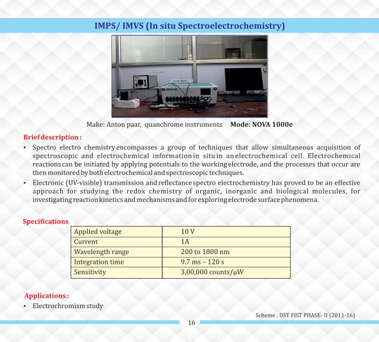
IMPS/ IMVS (In situ Spectroelectrochemistry)
Scheme : DST FIST PHASE- II (2011-16)
Brief description :
� Spectro electro chemistry encompasses a group of techniques that allow simultaneous acquisition ofspectroscopic and electrochemical information in situ in an electrochemical cell. Electrochemicalreactions can be initiated by applying potentials to the working electrode, and the processes that occur arethen monitored by both electrochemical and spectroscopic techniques.
� Electronic (UV-visible) transmission and re!lectance spectro electrochemistry has proved to be an effectiveapproach for studying the redox chemistry of organic, inorganic and biological molecules, forinvestigating reaction kinetics and mechanisms and for exploring electrode surface phenomena.
Speci!ications
Applied voltage
Current
Wavelength range
Integration time
Sensitivity
10 V
1A
200 to 1800 nm
9.7 ms – 120 s
3,00,000 counts/µW
17
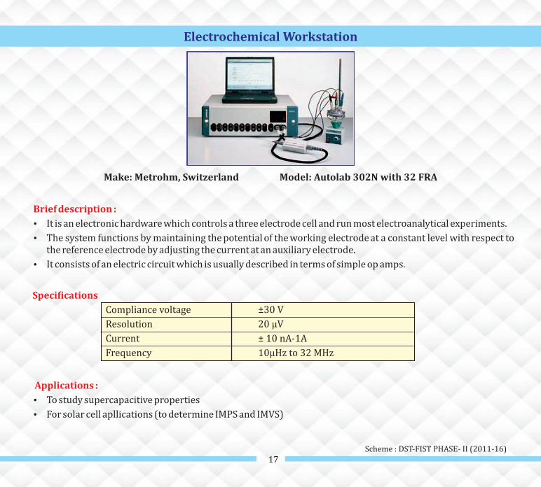
Applications :
� For solar cell apllications (to determine IMPS and IMVS)
� To study supercapacitive properties
Make: Metrohm, Switzerland Model: Autolab 302N with 32 FRA
Electrochemical Workstation
Scheme : DST-FIST PHASE- II (2011-16)
� It is an electronic hardware which controls a three electrode cell and run most electroanalytical experiments.
� The system functions by maintaining the potential of the working electrode at a constant level with respect tothe reference electrode by adjusting the current at an auxiliary electrode.
� It consists of an electric circuit which is usually described in terms of simple op amps.
Brief description :
Speci!ications
Compliance voltage
Resolution
Current
Frequency
±30 V
20 μV
± 10 nA-1A
10μHz to 32 MHz
18
� Accurate determination of glucose
� DNA detection
Applications :
� Study of Marine Petroleum Pollutants
� Detection of bacterial bio!ilms
� Sensing application such as gas sensors and biosensors
Make: HORIBA Instruments Model: Fluoromax - 4
Spectro!luorometer (PL)
Scheme : DST-PURSE PHASE- I (2011-2016)
� The properties of the !luorescence emission spectra are frequently used to identify substances, often includingtheir concentrations, and in other cases properties of a medium which in!luence details of the !luorescence.
� It measures the !luorescence or light emitted by different !luorescing objects.
Brief description :
� It includes Excitation of !luorescence at multiple wavelengths caused by the excitation with light at a singlewavelength.
Speci!ications
Excitation
Emission
Wavelength Accuracy
Scan Speed
Signal to noise ratio
200-950 nm
200-950 nm
+ 0.5 nm
80 nm/s
3000:1 (Steady-state-mode)
19
� The pro!iler incorporates an optical de!lection height measurement mechanism and magneto static forcecontrol system
� The XP-1 uses a diamond stylus to lightly contact the surface
Brief description :
� Advanced computer controlled Stylus Pro!iling System for morphology/topography characterization ofsamples
Applications :
� Measures roughness, waviness and height (thickness) in variety of application
� Ability to measure precision step height from 10 angstroms to 100 microns
Make : Ambios technology(USA) Model : XP-1
Surface Pro!iler
Scheme : DST-FIST PHASE- I (2002-2007)
Speci!icationsSample stage diameter
M
Lateral resolution
Operating temperature
Vertical resolution
ax Power Requirements
170mm
100nm
11 to 21°C
1.5A-
220V
20
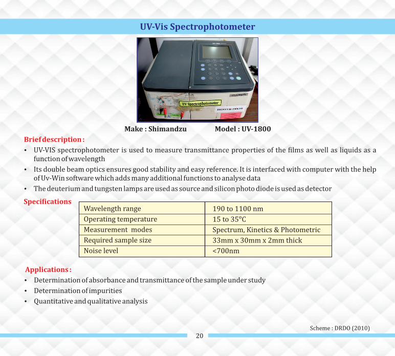
Brief description :
� UV-VIS spectrophotometer is used to measure transmittance properties of the !ilms as well as liquids as afunction of wavelength
� Its double beam optics ensures good stability and easy reference. It is interfaced with computer with the helpof Uv-Win software which adds many additional functions to analyse data
� The deuterium and tungsten lamps are used as source and silicon photo diode is used as detector
Applications :
� Determination of absorbance and transmittance of the sample under study
� Quantitative and qualitative analysis
� Determination of impurities
Make : Shimandzu Model : UV-1800
UV-Vis Spectrophotometer
Scheme : DRDO (2010)
Speci!icationsWavelength range
Operating temperature
Measurement modes
Required sample size
Noise level
190 to 1100 nm
15 to 35 C
Spectrum, Kinetics & Photometric
33mm x 30mm x 2mm thick
<700nm
.
21
� The 5½-digit Model 6514 is designed for applications that demand fast, yet precise measurements of low
currents, voltages from high resistance sources, charges, or high resistances
Brief description :
� The Model 6514 Electrometer combines !lexible interfacing capabilities with current sensitivity, charge