Vineet Pancholi, Sr Director, Test Technology Amkor Technology, Inc. AS DIGITAL SEMICONDUCTOR devices have become more powerful and the number of devices per system have grown, there is an increased need to move larger amounts of data at higher speeds between the devices and the external world. This has led to an explo- sion in the number and types of high- speed digital serial interfaces. In addi- tion, all popular high-speed digital serial interface standards have increasing data rate roadmaps. As each new generation of these interfaces have ever increasing performance and functionality, they pose significant test challenges. These high-speed digital serial interfaces for logical processors include Peripheral Component Interconnect Express (PCI Express or PCIe), Ether- net, Interlaken, Display Serial Interface (DSI), MIPI DigRF (M-PHY, D-PHY, C-PHY), Thunderbolt and others. Another important digital interface for processors is JEDEC’s Wide I/O vola- tile memory controller interface. Logic processors are employed in a variety of applications which include but are not limited to computer processors, network processors, graphics processors, artificial intelligence (AI) processors, applications processors found on mobile devices and embedded processors found in applica- tions like point-of-sale systems. PCIe is by far the most popular high-speed digi- tal serial test interface for inter-IC com- munications. The PCIe standard allows the single root complex processor to send and receive data to multiple peripheral component end points [1] . With the ever- increasing demand for faster and faster compute capabilities, the need to transmit and receive data between the processor and peripherals within the application has increased as well. PCIe data rates have increased with every release generation, 2.5 Gbps, 5 Gbps, 8 Gbps, 16 Gbps and Challenges of Advanced High-Speed Digital Product Test TECHNOLOGY based functional test (SBFT), built in self-test (BIST), and custom content, the physical layer (PHY, physical front end – Tx and Rx) is production tested with an on-load board loop back Design For Excellence (DFX) technique. Typical, production load boards utilize low-loss relays to allow switching between loop back signal paths and DC test of the I/O. HIGH-SPEED DIGITAL I/O LOGIC The Serializer/Deserializer (SerDes I/Os have transaction, data link and the physical blocks that are responsible for formatting the transmitted and received data (See Figure 2). are expected to hit 32 Gbps in the not-so- distant future. Similar increases in data rates have also been observed for non- PCIe high-speed digital serial interfaces. Recently, USB3.x and Thunderbolt with their higher data rates have gained popu- larity for externally pluggable power, storage and display peripherals to the application platform. Figure 1 shows an example of possible processor outputs. None of these high-speed serial digital interfaces full signal chains are functionally tested in production at their native data rate with a matching automat- ic test equipment (ATE) digital instru- mentation. Popular ATEs include tester platforms from vendors like Advantest, Teradyne, Cohu and others. The data rate sweet spot of pin electronics for digital instrumentation on these tester platforms is between 1.6 Gbps and 3.2 Gbps. This data rate is sufficient to drive scan test content used to test the logic cells on these processors. While most of the die’s logic area is tested with scan, structural SPRING 2021 MEPTEC REPORT | 13 meptec.org Figure 2. PCIe high-level block diagram [2] . Ethernet Tx P/N [0,1] Ethernet Rx P/N [0,1] Pure Clock (100 MHz) D+ Pure Clock (100 MHz) D- PCIe Tx P/N [0,3] PCIe Rx P/N [0,3] USB3 Rx P/N [0,3] USB3 Tx P/N [0,3] V REF Interlaken Tx P/N [0,15] Slow Speed Serial I 2 C. SPI. UART JTAG TAP Display Tx P/N Display Rx P/N DUT Ground Interlaken Rx P/N [0,15] FIVR Input Voltage Rails DDQ Bus 64 Bit I/O [0,1] DDQ Strobe Bus Processor (DUT) Figure 1. High-level block diagram and interfaces including fully integrated voltage regulator (FIVR) input.
Transcript
Vineet Pancholi, Sr Director, Test TechnologyAmkor Technology, Inc.
AS DIGITAL SEMICONDUCTOR devices have become more powerful and the number of devices per system have grown, there is an increased need to move larger amounts of data at higher speeds between the devices and the external world. This has led to an explo-sion in the number and types of high-speed digital serial interfaces. In addi-tion, all popular high-speed digital serial interface standards have increasing data rate roadmaps. As each new generation of these interfaces have ever increasing performance and functionality, they pose significant test challenges. These high-speed digital serial interfaces for logical processors include Peripheral Component Interconnect Express (PCI Express or PCIe), Ether-net, Interlaken, Display Serial Interface (DSI), MIPI DigRF (M-PHY, D-PHY, C-PHY), Thunderbolt and others. Another important digital interface for processors is JEDEC’s Wide I/O vola-tile memory controller interface. Logic processors are employed in a variety of applications which include but are not limited to computer processors, network processors, graphics processors, artificial intelligence (AI) processors, applications processors found on mobile devices and embedded processors found in applica-tions like point-of-sale systems. PCIe is by far the most popular high-speed digi-tal serial test interface for inter-IC com-munications. The PCIe standard allows the single root complex processor to send and receive data to multiple peripheral component end points [1]. With the ever-increasing demand for faster and faster compute capabilities, the need to transmit and receive data between the processor and peripherals within the application has increased as well. PCIe data rates have increased with every release generation, 2.5 Gbps, 5 Gbps, 8 Gbps, 16 Gbps and
Challenges of Advanced High-SpeedDigital Product Test
TECHNOLOGY
based functional test (SBFT), built in self-test (BIST), and custom content, the physical layer (PHY, physical front end – Tx and Rx) is production tested with an on-load board loop back Design For Excellence (DFX) technique. Typical, production load boards utilize low-loss relays to allow switching between loop back signal paths and DC test of the I/O.
HIGH-SPEED DIGITAL I/O LOGIC The Serializer/Deserializer (SerDes I/Os have transaction, data link and the physical blocks that are responsible for formatting the transmitted and received data (See Figure 2).
are expected to hit 32 Gbps in the not-so-distant future. Similar increases in data rates have also been observed for non-PCIe high-speed digital serial interfaces. Recently, USB3.x and Thunderbolt with their higher data rates have gained popu-larity for externally pluggable power, storage and display peripherals to the application platform. Figure 1 shows an example of possible processor outputs. None of these high-speed serial digital interfaces full signal chains are functionally tested in production at their native data rate with a matching automat-ic test equipment (ATE) digital instru-mentation. Popular ATEs include tester platforms from vendors like Advantest, Teradyne, Cohu and others. The data rate sweet spot of pin electronics for digital instrumentation on these tester platforms is between 1.6 Gbps and 3.2 Gbps. This data rate is sufficient to drive scan test content used to test the logic cells on these processors. While most of the die’s logic area is tested with scan, structural
SPRING 2021 MEPTEC REPORT | 13meptec.org
Figure 2. PCIe high-level block diagram [2].
Ethernet Tx P/N [0,1]
Ethernet Rx P/N [0,1]
Pure Clock (100 MHz) D+
Pure Clock (100 MHz) D-
PCIe Tx P/N [0,3]
PCIe Rx P/N [0,3]
USB3 Rx P/N [0,3]
USB3 Tx P/N [0,3]
VREF
Interlaken Tx P/N [0,15]
Slow Speed SerialI2C. SPI. UART
JTAG TAP
Display Tx P/N
Display Rx P/N
DUT Ground
Interlaken Rx P/N [0,15]
FIVR InputVoltage Rails
DDQ Bus 64 Bit I/O [0,1]
DDQ Strobe Bus
Processor(DUT)
Figure 1. High-level block diagram and interfaces including fully integrated voltage regulator (FIVR) input.
The physical block includes the SerDes and data encoder/decoder seg-ments. The logic implementation layers are tested with scan, BIST and SBFT logic content.
HIGH-SPEED DIGITAL I/O SIGNALS Production testing of the high-speed SerDes interface requires load board development that presents a test environ-ment which mimics the application’s design environment in terms of signal path impedance loading. This means that the device under test (DUT) is powered with a clean power source and reference clocks (not shown in Figure 2). Typical test methodologies use common refer-ence clock Rx architectures, which dis-tribute the single common clock to both the Tx phase-locked loop (PLL) and Rx PLL. The loop back differential signal traces connecting the Tx to the Rx are matched within reason and present a bal-anced 100-Ω differential pair trace width. AC-coupled paths include capacitors in the loop back paths.
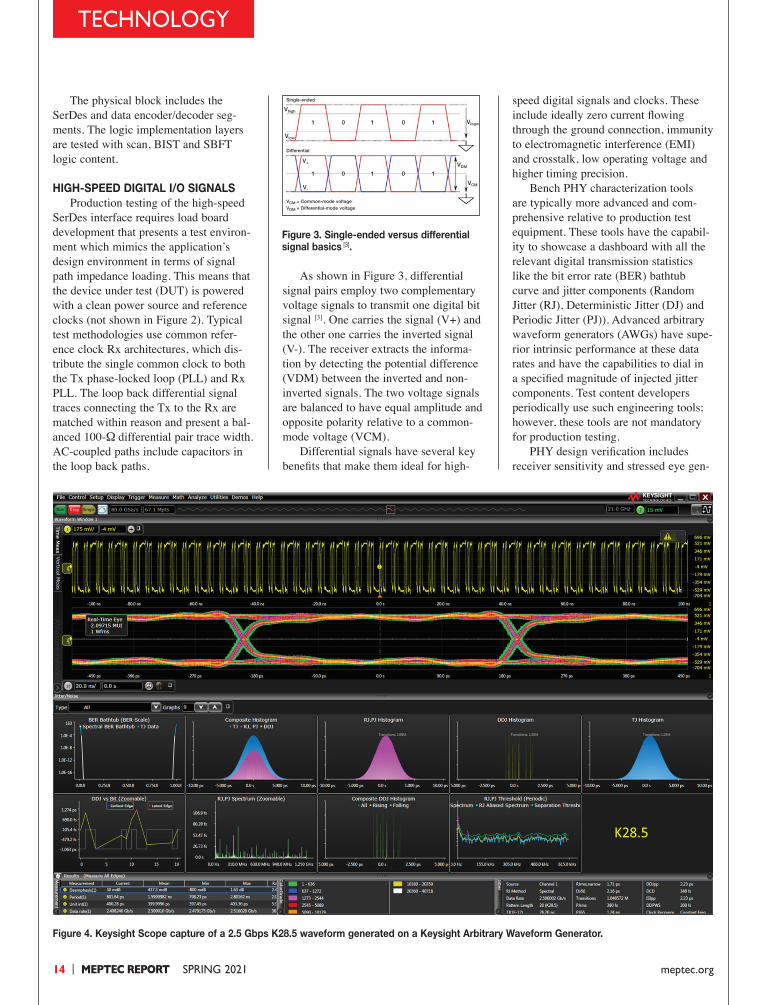
Figure 4. Keysight Scope capture of a 2.5 Gbps K28.5 waveform generated on a Keysight Arbitrary Waveform Generator.
As shown in Figure 3, differential signal pairs employ two complementary voltage signals to transmit one digital bit signal [3]. One carries the signal (V+) and the other one carries the inverted signal (V-). The receiver extracts the informa-tion by detecting the potential difference (VDM) between the inverted and non-inverted signals. The two voltage signals are balanced to have equal amplitude and opposite polarity relative to a common-mode voltage (VCM). Differential signals have several key benefits that make them ideal for high-
speed digital signals and clocks. These include ideally zero current flowing through the ground connection, immunity to electromagnetic interference (EMI) and crosstalk, low operating voltage and higher timing precision. Bench PHY characterization tools are typically more advanced and com-prehensive relative to production test equipment. These tools have the capabil-ity to showcase a dashboard with all the relevant digital transmission statistics like the bit error rate (BER) bathtub curve and jitter components (Random Jitter (RJ), Deterministic Jitter (DJ) and Periodic Jitter (PJ)). Advanced arbitrary waveform generators (AWGs) have supe-rior intrinsic performance at these data rates and have the capabilities to dial in a specified magnitude of injected jitter components. Test content developers periodically use such engineering tools; however, these tools are not mandatory for production testing. PHY design verification includes receiver sensitivity and stressed eye gen-
Figure 3. Single-ended versus differential signal basics [3].
Vlogic
Vlow
Vhigh
VCM
VDM
Single-ended
V+
V-
Differential
VCM = Common-mode voltageVDM = Differential-mode voltage
eration, transmitter tests, DC tests and timing verification (See Figure 4). Signal bus timing and levels are tested during production testing, while intrinsic jitter and the impact of injected jitter are most-ly characterized on the bench. The test methodology (and hence the Tx and Rx test list) does depend on the process technology and the end application. High data rate or high clock rate differ-ential signals have a smaller eye height and width - the higher the data rate, the higher the transmission parasitic losses. Therefore, signal path optimization is critical. Also, Table 1 shows how test intervals tighten with increasing data rate.
HIGH-SPEED PRODUCTION ASSEMBLY PACKAGES Several advanced packages such as flip chip ball grid array (FCBGA), Flip Chip chip scale packaging (fcCSP) and other qualified packages support all the high-speed digital requirements. The die package includes parasitic components including impairments added to the Tx and Rx signal paths from the bump or bond wire, the substrate trace and the solder ball [4, 5] as modeled in Figure 5. Advanced packages require a rigor-ous package qualification process. This process includes all thermal, mechani-cal and electrical package performance aspects of qualification. As part of electrical package qualification, all new performance envelope extensions are simulated and then verified with an elec-trical verification loop. Each customer product has unique application require-ments in terms of operating frequencies and bandwidth. The package design team routinely performs custom simula-tions for high-speed digital signal paths. Critical shapes, geometrical dimensions, package assembly processing and mate-rial type determine the overall package performance [6]. The simulations ensure right-the-first-time success with perfor-mance targets of insertion loss better than
-3 dB, return loss better than -10 dB and the signal-to-signal crosstalk better than -45 dB at specific operating regions.
HIGH-SPEED PRODUCTION TEST ENVIRONMENT Potential impairments to the signal path are an integral part of the produc-tion test tooling environment. The socket pogo pin, the material type, the signal pads, the surface traces and vias on the load board impact the overall perfor-mance metrics. These design consider-ations are important even to implement loop back of these signals (see Figure 6). Improper ground shielding of differential pairs, via stubs and inadequate equiva-
lent series resistance (ESR) surface mount components can result in sub-par performance. The socket and printed circuit board (PCB) material type play an important role. Good trace layout design guidelines, like top layer traces without vias and ground stitches along the trace path, can ensure minimal crosstalk. Higher and higher data rates exacerbate the impacts of all these impairments. Test development teams work closely with the probe card and load board design house to ensure all production test requirements are met. The requirements for different appli-cations can vary greatly. For example. server applications are data transaction
Table 1. Unit intervals for popular data rates.
Figure 6. PCIe on load board loop back to enable production testing of the PHY [7].
S-BallTx+
S-BallTx-
S-BallRx+
S-BallRx-
PadTx+
PadTx-
PadRx+
PadRx-
Load Board
100Ω PCBDifferential Traces
DU
T P
in
Socket Pin
Socket
Socket Pin
Socket Pin
Socket Pin
Pcle Tx-
Pcle Tx+
Pcle Tx-
Pcle Tx+
Figure 5. Die-to-package pin out parasitic components contributing to the performance.
intensive with several concurrent high-speed channels for effective bandwidth. Desktop applications are not as power hungry and may require fewer high-speed digital transmit and receive ports. Mobile applications (handhelds and wearables) are battery powered and have a limited number of extreme data rate requirements. By design, server and desktop applications may be able to afford molded packages like FCBGA and fcCSP or stacked die within a Package-on-Package (PoP), while mobile applica-tions may require die or Wafer Level Chip Scale Packaging (WLCSP) designs. In some cases, the end application may also mandate extended temperature and humidity operation. For example, auto-motive and military ranges are more stringent relative to consumer, com-mercial and industrial operation. These variations require production testers and material handling (prober and handler) capabilities for the whole gamut of pack-age types and applications. An experienced test development team carefully architect the test pro-gram’s test list sequence to ensure each functional block is tested to enable streamlined and efficient test execution flow. The purpose of structural scan test pattern content is to identify silicon IC fabrication and assembly packaging defects. The typical high-level production test flow includes these test insertions – Wafer Probe, Burn In, Final Test and System Level Test – prior to customer-specific backend processing and shipping instructions. The end user application noted above may mandate customization of the test flow and test limits. Crosstalk between multiple I/O lanes may be mini-mized by testing these lanes sequentially, if the number of lanes to test are small and the test time for each lane is small. In the case of PCIe, the end applica-tion for the customer part might be a root complex, a bridge or an end point. The high-speed digital production test inter-face handling is similar. Experienced test development teams have the expertise to develop test content and production test-ing for each product application type. Most processor architectures in this category implement a dedicated Design for Test (DFT) Test Access Port (TAP), which is IEEE 1149.1 compliant [8]. This five-pin serial I/O interface is typically
dedicated for test access to the DUT. The standard allows implementation of both public and private instructions with access to custom device test features. With increasing digital logic and hence the need of additional test content, a new higher speed TAP interface has recently been proposed with the IEEE 1149.10
[9] standard. IEEE 1149.1 TCK rates of up to 100 MHz have served the industry well for over two decades. In some cases, TAP is used to write specific device fuse bits or to load test content via test pat-terns into the DUT to initiate tests like BIST or to read out scan results. The TAP may include DFX access to high-speed I/O structures in addition to other useful test features not mentioned in this article. Test developers may use such DFX device features for production test-ing of these high-speed interfaces. Advanced production testers include digital sub-system instrumentation from vendors like Advantest, Teradyne, Cohu, NI and others. Advantest’s V93K and T2000 testers, Teradyne’s UFlex, J750 and other family of testers, Cohu’s Diamondx and PAx testers each have digital pin electronics with a slightly different scan test implementation. Dif-ferent performance envelopes of these testers cater to the variety of customer products with a variety of scan data I/O clock rates over 500 MHz, modulo 2, 4, 8, 16 channels, memory depths over 10s of giga-vectors, impacts to load board designs and multisite capabilities. This results in offering scan content solutions at a variety of price points. The objective is to make testing easier by providing a simple way to set and observe every flip-flop in the DUT. Full scan design implementations use automatic test pat-tern generation (ATPG). These designs do not require sequential pattern genera-tion and combinatorial tests are much easier to generate by the device designer, for adequate test coverage. Experienced production test developers routinely help implement such tests for customer devices.
SUMMARY High-speed serial digital interface I/O test data rates continue to increase towards 32 Gbps. The present ATEs do not provide test solutions for production test of these interfaces at their native
speeds, primarily relying on scan to test out fabrication defects. While bench characterization using differential sig-nal techniques can verify designs, they cannot be deployed as production test solutions. Experienced test development teams can circumvent the ATE deficien-cies that may be expensive to address by implementing DFX, BIST and signal path calibration. The loop back technique extends the ATE life and enables testing at native data rates. This requires extend-ing the calibration plane on the probe cards, load-boards and sockets to the device under test. When implemented, this technique provides an accurate, at-speed and cost-competitive test solution. Production test equipment cost is kept in control with DFX test methods that allow testing the PHY with on load board loop back. With its experience as a leading packaging supplier, Amkor has the nec-essary test tools to help customers with advanced production test implementa-tions. ◆
REFERENCES
[1] PCI Express® Base Specification, Revision 3.1a.
[2] PCI Express® Test Attribute Specification comparison by generation, Internet Source.
[3] Differential signal, Internet Source.
[4] High-Speed Differential Interconnection Design for Flip-Chip BGA Packages, Internet Source.
[5] Package Model Proposal, Internet Source.
[6] M. F. Caggiano, J. Ou, S. Bulumulla and D. Lischner, “RF electrical measurements of fine pitch BGA packages,” in IEEE Transactions on Components and Packag- ing Technologies, vol. 24, no. 2, pp. 233-240, June 2001, doi:10.1109/ 6144.926388.
[7] S. Arora, A. Aflaki, S. Biswas and M. Shimanouchi, “SERDES external loop back test using production parametric-test hardware,” 2016 IEEE International Test Conference (ITC), Fort Worth, TX, 2016, pp. 1-7, doi: 10.1109/TEST.2016.7805841.
[8] IEEE 1149.1-2013 - IEEE Standard for Test Access Port and Boundary-Scan Architecture, Internet Source.
[9] IEEE 1149.10-2017 - IEEE Standard for High-Speed Test Access Port and On-Chip Distribution Architecture, Internet Source.