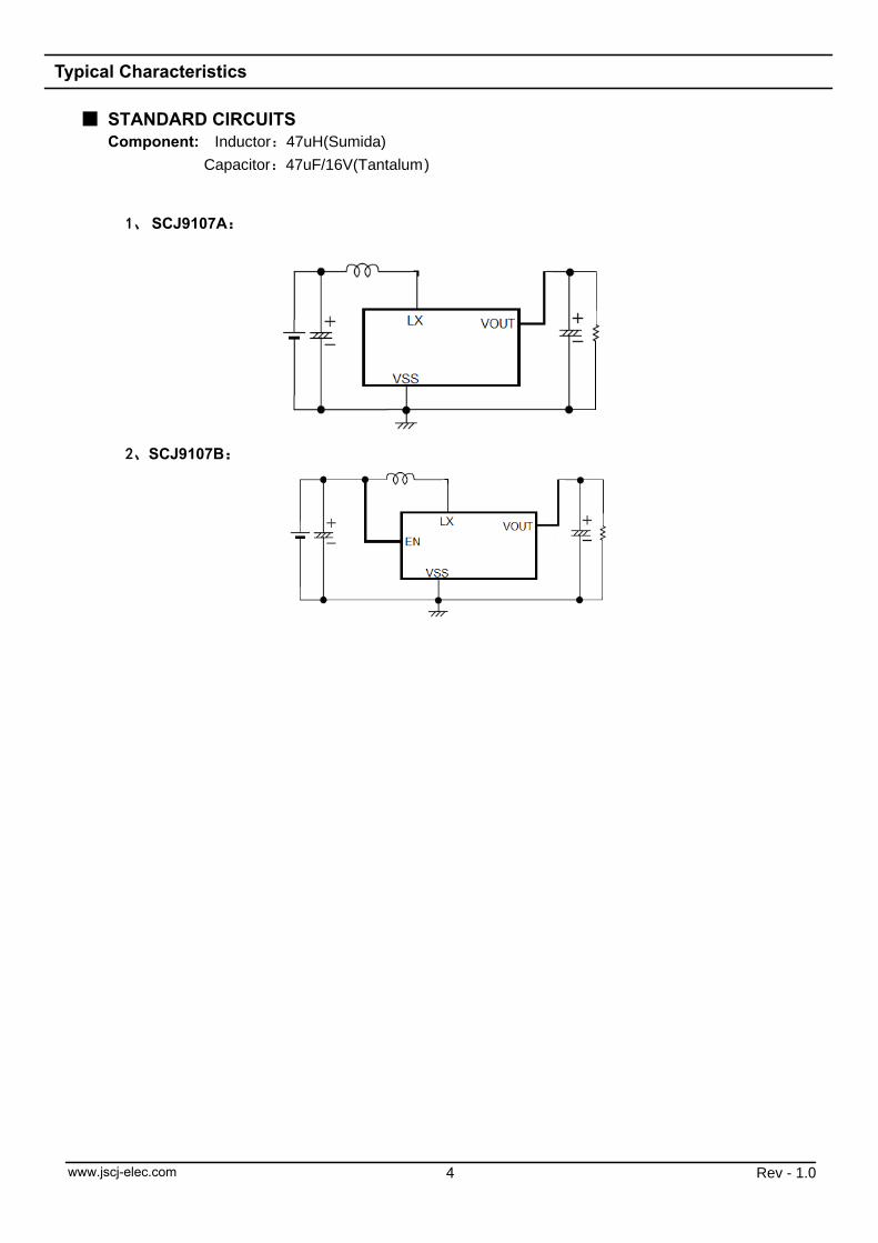
INTRODUCTION The CJ9107 Series is a Synchronous step-up DC/DC Converter with PFM Control. With the CJ9107 Series, a step-up switching DC/DC converter can be configured by using an external coil, capacitor. The built-in MOSFET is turned off by a protection circuit when the voltage at the LX pin exceeds the limit to prevent it from being damaged. FEATURES External parts: Coil, capacitor Output voltage: Settable to between 2.1V to 5.5 V in 0.1 V steps Maximum Oscillation frequency:300KHz Accuracy of ±2% High efficiency:95% APPLICATIONS Digital cameras Electronic notebooks and PDAs Portable CD/MD players Cameras, video equipment, Communications equipment Power supply for microcomputers BLOCK DIAGRAM LX EN VOUT VSS Current Limiting comparator buffer PFM control OSC Chip Enable ref Error Amplifier DESIGNATOR SYMBOL DESCRIPTION ① A Standard LX B With shutdown, LX ②③ Integer Output Voltage (2.1~5.5) e.g.:3.0V=②:3 ; ③:0 ④ T3/T5 Package:SOT-23-3/5L K Package:SOT-23 R Package:SOT-89-3L L Package:TO-92 Synchronous Step-Up DC/DC Converter with PFM Control CJ9107 Series DEVICE INFORMATION: 1 Rev - 1.0 CJ9107 ①②③④ JIANGSU CHANGJING ELECTRONICS TECHNOLOGY CO., LTD www.jscj-elec.com
Transcript
INTRODUCTIONThe CJ9107 Series is a Synchronous
step-up DC/DC Converter with PFM Control.
With the CJ9107 Series, a step-up
switching DC/DC converter can be configured
by using an external coil, capacitor. The
built-in MOSFET is turned off by a protection
circuit when the voltage at the LX pin exceeds
the limit to prevent it from being damaged.
FEATURES External parts: Coil, capacitor
Output voltage: Settable to between 2.1V
to 5.5 V in 0.1 V steps
Maximum Oscillation frequency:300KHz
Accuracy of ±2%
High efficiency:95%
APPLICATIONS Digital cameras
Electronic notebooks and PDAs
Portable CD/MD players
Cameras, video equipment,
Communications equipment
Power supply for microcomputers
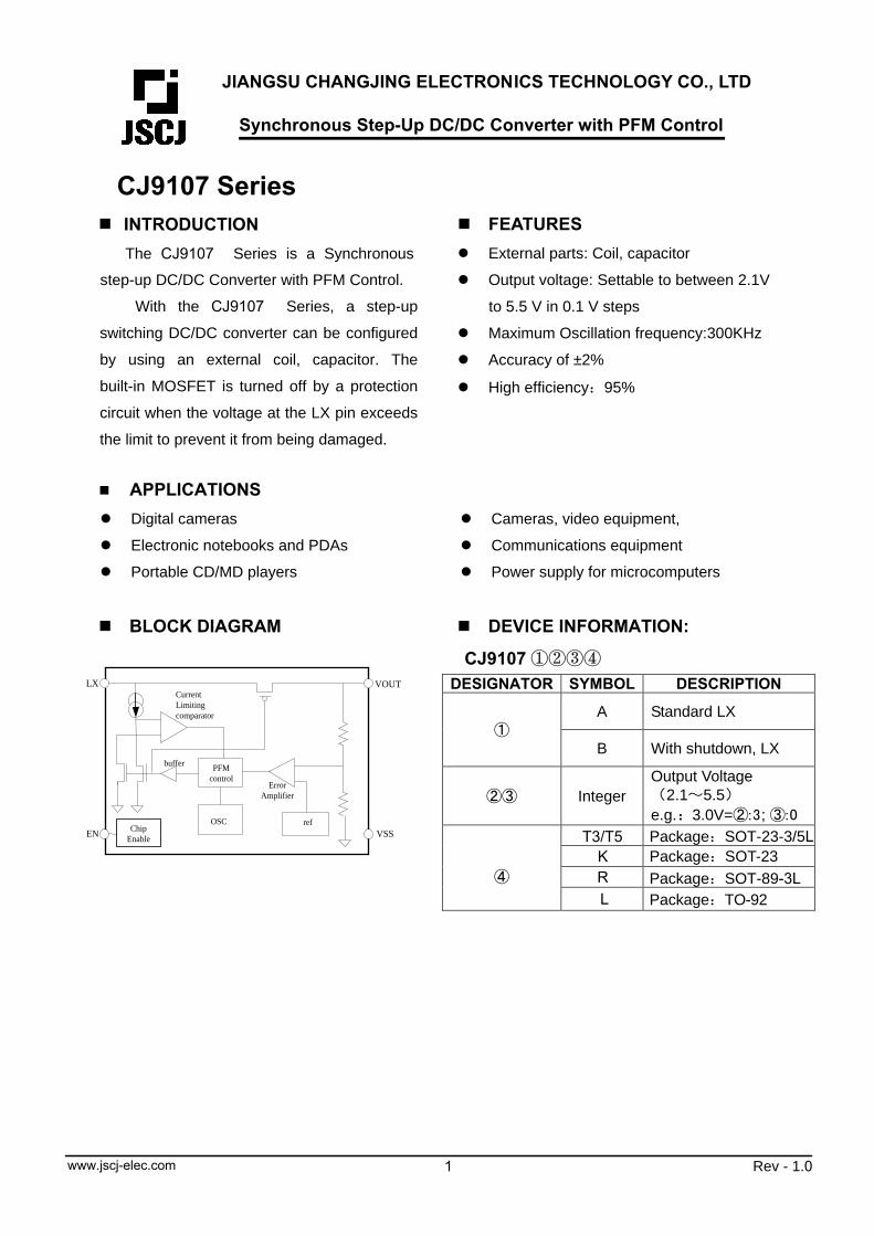
BLOCK DIAGRAM
LX
EN
VOUT
VSS
CurrentLimitingcomparator
buffer PFMcontrol
OSCChip
Enable
ref
ErrorAmplifier
DESIGNATOR SYMBOL DESCRIPTION
①A Standard LX
B With shutdown, LX
②③ Integer Output Voltage (2.1~5.5) e.g.:3.0V=②:3; ③:0
④
T3/T5 Package:SOT-23-3/5L K Package:SOT-23 R Package:SOT-89-3L L Package:TO-92
Synchronous Step-Up DC/DC Converter with PFM Control
CJ9107 Series
DEVICE INFORMATION:
1 Rev - 1.0
CJ9107①②③④
JIANGSU CHANGJING ELECTRONICS TECHNOLOGY CO., LTD
www.jscj-elec.com
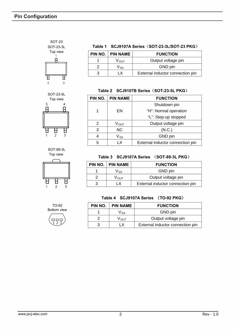
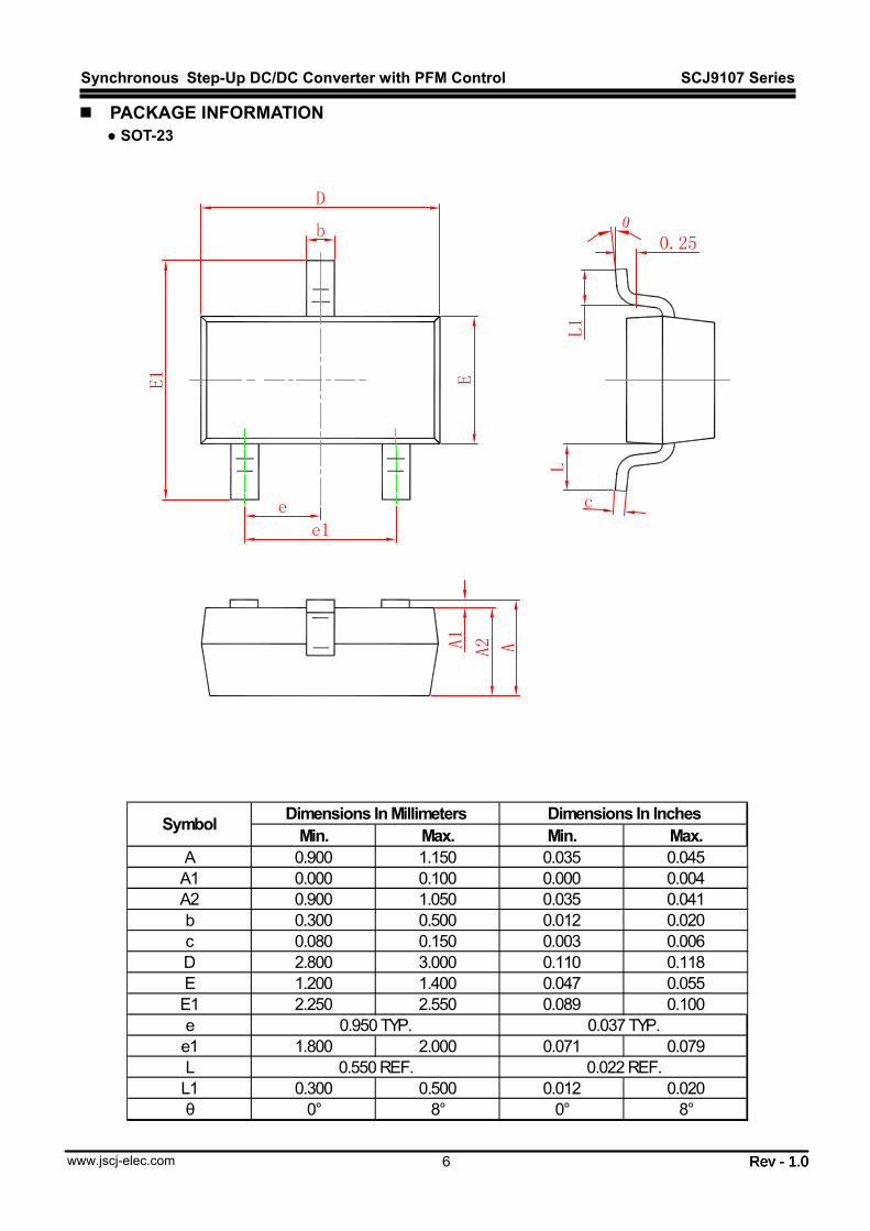
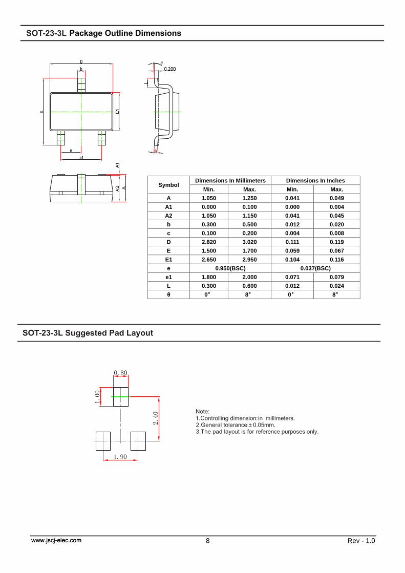
Table 1 SCJ9107A Series(SOT-23-3L/SOT-23 PKG)
PIN NO. PIN NAME FUNCTION 1 V Output voltage pin OUT 2 V GND pin SS 3 LX External inductor connection pin
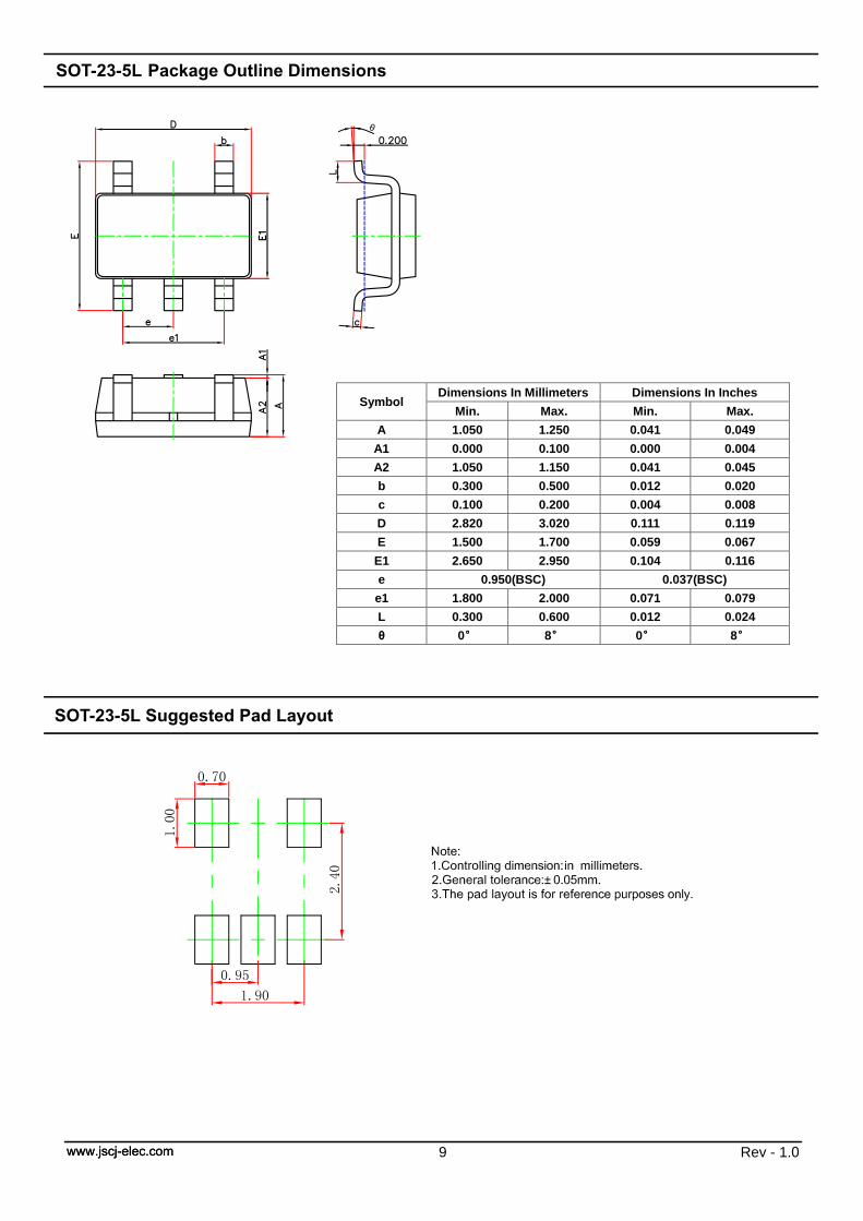
Table 2 SCJ9107B Series(SOT-23-5L PKG)
PIN NO. PIN NAME FUNCTION
1 EN Shutdown pin
“H”: Normal operation “L”: Step-up stopped
2 V Output voltage pin OUT 3 NC (N.C.) 4 V GND pin SS 5 LX External inductor connection pin
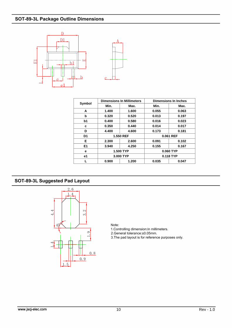
Table 3 SCJ9107A Series (SOT-89-3L PKG)
PIN NO. PIN NAME FUNCTION 1 V GND pin SS 2 V Output voltage pin OUT 3 LX External inductor connection pin
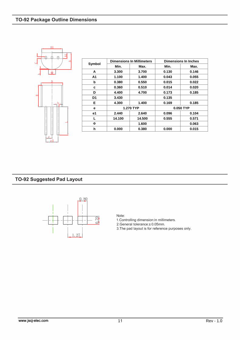
Table 4 SCJ9107A Series (TO-92 PKG)
PIN NO. PIN NAME FUNCTION 1 V GND pin SS 2 V Output voltage pin OUT 3 LX External inductor connection pin 1 2 3
TO-92 Bottom view
2 Rev - 1.0
SOT-23SOT-23-3L Top view
SOT-23-5L Top view
SOT-89-3L Top view
Pin�$onfiguration
www.jscj-elec.com
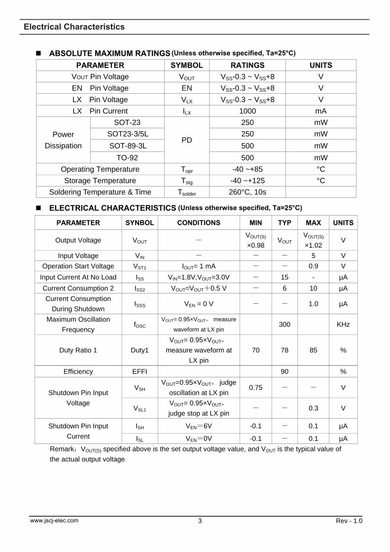
ABSOLUTE MAXIMUM RATINGSPARAMETER SYMBOL RATINGS UNITS
VOUT Pin Voltage VOUT VSS-0.3 ~ VSS+8 V EN Pin Voltage EN VSS-0.3 ~ VSS+8 V LX Pin Voltage VLX VSS-0.3 ~ VSS+8 V LX Pin Current ILX 1000 mA
Power Dissipation
SOT-23
PD
250 mW SOT23-3/5L 250 mW SOT-89-3L 500 mW
TO-92 500 mW Operating Temperature Topr -40 ~+85 °C Storage Temperature Tstg -40 ~+125 °C
IMPORTANT NOTICE, PLEASE READ CAREFULLYThe information in this data sheet is intended to describe the operation and characteristics of our products. JSCJ has the right to make any modification, enhancement, improvement, correction or other changes to any content in this data sheet, including but not limited to specification parameters, circuit design and application information, without prior notice. Any person who purchases or uses JSCJ products for design shall: 1. Select products suitable for circuit application and design; 2. Design, verify and test the rationality of circuit design; 3. Procedures to ensure that the design complies with relevant laws and regulations and the requirements of such laws and regulations. JSCJ makes no warranty or representation as to the accuracy or completeness of the information contained in this data sheet and assumes no responsibility for the application or use of any of the products described in this data sheet. Without the written consent of JSCJ, this product shall not be used in occasions requiring high quality or high reliability, including but not limited to the following occasions: medical equipment, automotive electronics, military facilities and aerospace. JSCJ shall not be responsible for casualties or property losses caused by abnormal use or application of this product.