CMOS LNA DESIGN FOR MULTI-STANDARD APPLICATIONS Masters thesis performed at Electonic Devices Linköpings Institute of Technology by Muhammad Wasim Reg nr: LiTH-ISY-EX--06/3813--SE Linköping 2006-09-26
Transcript
CMOS LNA DESIGN FOR MULTI-STANDARD APPLICATIONS
Masters thesis performed at Electonic Devices
Linköpings Institute of Technology
by
Muhammad Wasim
Reg nr: LiTH-ISY-EX--06/3813--SE
Linköping 2006-09-26
CMOS LNA DESIGN FOR MULTI-STANDARD APPLICATIONS
Masters thesis performed at Electonic Devices
Linköpings Institute of Technology
by
Muhammad Wasim
Reg nr: LiTH-ISY-EX--06/3813--SE
Supervisor: Assoc. Prof. Jerzy Dabrowski
Examiner: Assoc. Prof. Jerzy Dabrowski
Linköping, 11 November 2006.
Presentation Date
2006-09-26Publishing Date (Electronic version)
2006-11-13
Department and DivisionElectronic DevicesDepartment of Electrical Engineering
URL, Electronic Versionhttp://www.ep.liu.se
Publication Title
CMOS LNA Design for Multi-standard applications
Author(s)
Muhammad Wasim
Abstract
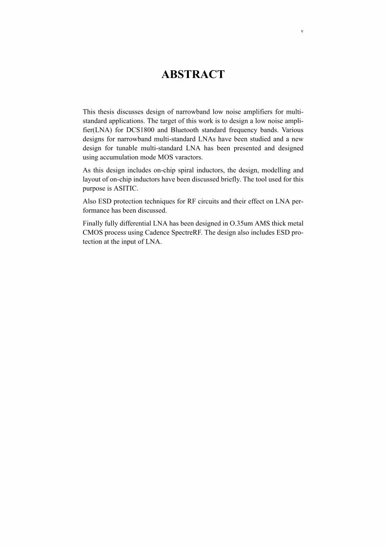
This thesis discusses design of narrowband low noise amplifiers for multistandard applications. The target of this work is to design a low noise amplifier(LNA) for DCS1800 and Bluetooth standard frequency bands. Various designs for narrowband multi-standard LNAs have been studied and a new design for tunable multi-standard LNA has been presented and designed using accumulation mode MOS varactors.
As this design includes on-chip spiral inductors, the design, modelling and layout of on-chip inductors have been discussed briefly. The tool used for this purpose is ASITIC.
Also ESD protection techniques for RF circuits and their effect on LNA performance has been discussed.
Finally fully differential LNA has been designed in O.35um AMS thick metal CMOS process using Cadence SpectreRF. The design also includes ESD protection at the input of LNA.
KeywordsLow noise amplifier, Radio frequency, ESD protection, Spiral inductors, DCS1800, Bluetooth
This thesis discusses design of narrowband low noise amplifiers for multi-standard applications. The target of this work is to design a low noise ampli-fier(LNA) for DCS1800 and Bluetooth standard frequency bands. Various designs for narrowband multi-standard LNAs have been studied and a new design for tunable multi-standard LNA has been presented and designed using accumulation mode MOS varactors.
As this design includes on-chip spiral inductors, the design, modelling and layout of on-chip inductors have been discussed briefly. The tool used for this purpose is ASITIC.
Also ESD protection techniques for RF circuits and their effect on LNA per-formance has been discussed.
Finally fully differential LNA has been designed in O.35um AMS thick metal CMOS process using Cadence SpectreRF. The design also includes ESD pro-tection at the input of LNA.
vi
vii
AKNOWLEDGEMENTS
First of all I would like to thank Professor Jerzy Dabrowski for providing me an opportunity to work on this project under his supervision and guiding me throughout the project.
I would also like to thank Rashad M. Ramzan for the help and advice throughout the project. I am also thankful to all members of Electronic Devices for their help during my thesis work.
I also wish to thank my family for their continious support and encourage-ment throughout my studies. I especially wish to thank my father Khalid Hus-sain, my mother, uncle Abdul Basit and elder brother Dr. Nadeem Sultan for continuous encouragement.
I am also thankful to my friends at Linköping for encouraging and supporting me when I needed their help.
6 Layout Issues 557 Conclusion and Future Work 578 References 59
1
1 INTRODUCTION
1.1 BACKGROUND
The growing demand of wireless application products demands low cost and highly integrable ICs for transceivers. The increasing number of wireless communication standards require transceivers that can handle multiple fre-quency bands and applications.
The first component of a wireless receiver front-end is a low noise amplifier. Its main function is to amplify the signal to suppress the noise of subsequent stages while adding as little noise as possible. For multi-standard receivers various wideband and concurrent dual-band low noise amplifier designs have been previously presented.
Inductive source degenerated low noise amplifiers are consider the best as they provide the best noise performance and gain however they operate in the narrow band of frequency of interest. In this thesis work an inductive source degenerated fully differential low noise amplifier has been presented which can be tuned to the required frequency of interest.
1.2 PURPOSE AND MOTIVATION
The purpose of this thesis is to study different architectures of LNA designs for multi-standard receiver front end and design LNA that can be used in the frequency range of 1.8GHz to 2.4GHz. The following goals are included in the design. • LNA should be switchable between the two frequency bands i.e. 1.8GHz
and 2.4GHz.• It should be process and temperature variation tolerant and should be able
to be tuned to required frequency.
2 CMOS LNA Design for Multi-standard Applications
• ESD protection methodology in accordance with 2kV human body model is to be studied and included in the design.
1.3 TARGET SPECIFICATIONS
The project consists of LNA design for reconfigurability in 0.35um CMOS process. The following target specs were set for this purpose
1.4 OUTLINE OF THESIS.
• Chapter 2- RF Basic concepts and receiver architecture short descrip-tion of RF basic fundamental, performance measures and receivers archi-tecture is discussed.
• Chapter 4- Reconfigureable LNA Design some previously designed multiband receiver LNAs are discussed and design for this LNA is pre-sented.
• Chapter 5- modelling, simulation and layout of inductors provides brief description of on-chip spiral inductors modelling and layout
• Chapter 6- Layout issues
• Chapter 7- Conclusion and future work
Narrow band Reconfigureable LNA design
Parameters Specificationsoperating frequency 1.8GHz -2.4GHzGain >15dBnoise figure <2.5dBInput matching 50 ohms -15dBIIP3 -10dBmStability Factor should be unconditionally
stable
3
1.5 TERMINOLOGY
IC Integrated circuitsRF Radio frequencyLNA Low noise amplifierIIP3 Input referred third order intermodulation intercept pointOIP3 Output referred third order intermodulation intercept pointCMOS Complementary metal oxide semiconductorRFIC Radio frequency integrated circuitsESD Electrostatic dischargefT Unity gain frequencyMIM Metal-insulator-metalIF Intermediate FrequencyLPF Low pass filterSDF Spectral Density Function
4 CMOS LNA Design for Multi-standard Applications
5
2 RF BASIC CONCEPTS AND RECEIVER
ARCHITECTURES
2.1 NOISE FIGURE.
Noise figure is commonly used to define additive noise of a circuit or system. Noise figure is the ratio of SNR at input to the SNR at output. it is a measure of degradation of SNR of a signal by the internal noise of an electronic cir-cuit. It can be described by the equation
(2.1)
or simply by
(2.2)
where Nin is the reference noise and G is the power gain of the corresponding stage given by
(2.3)
NF 10Sin Nin⁄
Sout Nout⁄------------------------⎝ ⎠
⎛ ⎞log=
NF 10NoutGNin------------⎝ ⎠
⎛ ⎞log=
G Sout Sin⁄=
6 CMOS LNA Design for Multi-standard Applications
2.1.1 NOISE FIGURE OF CASCADED STAGES.
Figure 2.1: Cascaded noisy stages
The noise figure of cascades stages shown in Fig. 2.1 is given by the Frii,s Formula as
(2.4)
2.2 SCATTERING PARAMETERS.
In RF systems design S-parameters play an important role due to the fact that at radio frequencies usual open and short circuit measurements are no longer applicable. At radio frequencies a short circuit does not behave as the same due to inductance of wire and same is the case with open circuit where we have capacitive behaviour. Due to this normal h-parameters and z-parameters are difficult to use. Moreover we are interested in measurement of incident and reflected wave power in a two-port network for RF blocks. S-parameters are the best way to describe these parameters of two-port networks.
2.2.1 DEFINITION OF S-PARAMETERS
S-parameters are used to define input-output relation of a network in the form of incident and reflected power.
Figure 2.2: Two-port network
NF1G1
SinNin
NF2G2
NF3G3
NFkGk
SoutNout
NF NF1NF2 1–
G1-------------------
NF3 1–G1G2
------------------- …NFk 1–
G1G2…Gk---------------------------+ + + +=
T w o -p o rtne tw o rk
Z o Z oE i1 E i2
E r1 E r2
7
The two-port network shown in Fig. 2.2 can be described as
(2.5)
where an represents the power wave travelling towards the two-port network and bn is the power wave reflected back from the two-port network given by
(2.6)
(2.7)
(2.8)
(2.9)
Here Ei and Er are the incident and reflected wave power respectively. The normalization by square root of Zo makes the square of an and bn terms equal to power of the incident and reflected wave respectively[1]. S11 is the input reflection coefficient, S21 is the forward gain relating output to input, S12 is the reverse transmission gain and S22 is the output reflection coefficient. We may derive mathematical expressions for these terms from (2.5) as
(2.10)
(2.11)
b1
b2
s11 s12
s21 s22
a1
a2
=
a1Ei1
Zo----------=
a2Ei2
Zo----------=
b1Er1
Zo----------=
b2Er2
Zo----------=
s11b1a1-----
a2 0=
=
s21b2a1-----
a2 0=
=
8 CMOS LNA Design for Multi-standard Applications
(2.12)
(2.13)
2.3 STABILITY.
Stability is an important characteristic of an amplifier design. The stability of a circuit is characterized by Stern stability factor given in (2.14).
(2.14)
(2.15)
Another stability measures is described by the Bif factor given by (2.16)
(2.16)
A circuit is unconditionally stable if K > 1 and Bif > 0.
2.4 INPUT AND OUTPUT IMPEDANCE MATCHING.
Input and output matching is an important phenomena in RF circuits and it plays important role in its performance. Input and output impedance match-ing is given by the input and output return loss and is defined as
Linearity is another important design consideration along with noise, gain and impedance matching. Active RF devices can be considered nonlinear in operation. These devices can generate undesirable spurious signal when driven by large input signal. Nonlinearities result in intermodulation distor-tion, desensitization and blocking and cross modulation. When a signal is applied to input of nonlinear system the output contains several harmonics of input signal which are integral multiples of input signal frequency. For exam-ple if input
(2.19)
is applied to nonlinear system, the output is given by
(2.20)
(2.21)
The term with the input frequency is called the fundamental and the higher order are called harmonics.
Two important measures of linearity of RF circuits are 1-dB compression point and third-order intercept point(IP3).
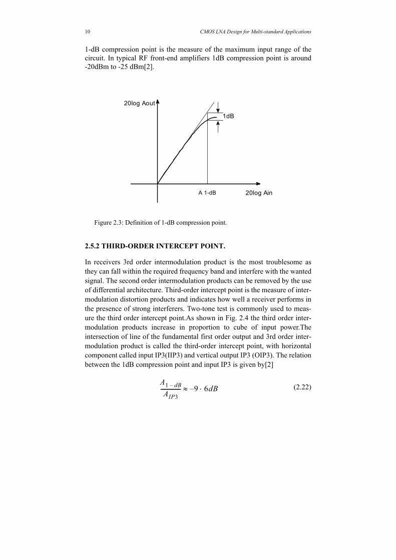
2.5.1 1-DB COMPRESSION POINT
If an amplifier is driven by a sufficient high input signal, the gain of the amplifier starts to drop at a certain level of input. This phenomenon is known as gain compression. 1-dB compression point is the measure of gain compres-sion and is defined as the input signal level for which the gain of the amplifier drops by 1-dB as seen in Fig. 2.3.
20 Γoutlog 20 s22log=
x t( ) A ωtcos=
y t( ) α1A ωtcos α2A2cos2ωt α3A3cos3ωt+ +=
y t( ) α2A2
2------------ α1A 3α3
4---------+⎝ ⎠⎛ ⎞ ωtcos
α2A2
2------------ 2ωtcosα3A3
4------------ 3ωtcos+ + +=
10 CMOS LNA Design for Multi-standard Applications
1-dB compression point is the measure of the maximum input range of the circuit. In typical RF front-end amplifiers 1dB compression point is around -20dBm to -25 dBm[2].
Figure 2.3: Definition of 1-dB compression point.
2.5.2 THIRD-ORDER INTERCEPT POINT.
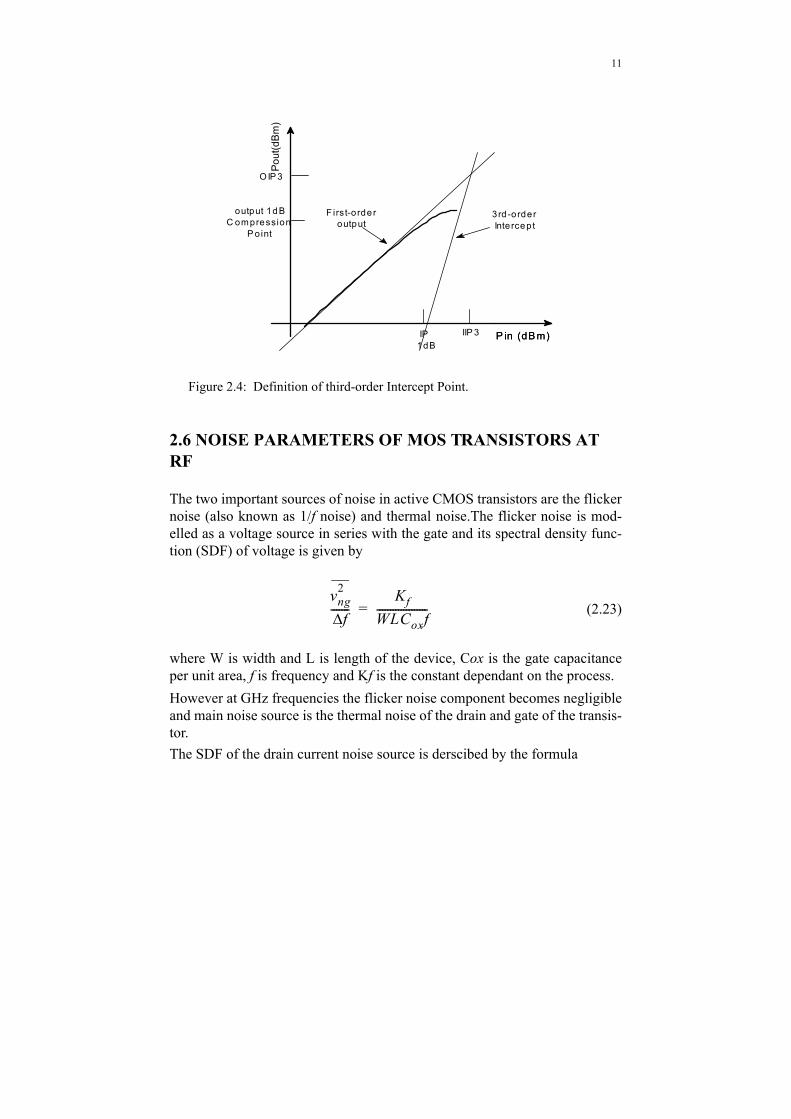
In receivers 3rd order intermodulation product is the most troublesome as they can fall within the required frequency band and interfere with the wanted signal. The second order intermodulation products can be removed by the use of differential architecture. Third-order intercept point is the measure of inter-modulation distortion products and indicates how well a receiver performs in the presence of strong interferers. Two-tone test is commonly used to meas-ure the third order intercept point.As shown in Fig. 2.4 the third order inter-modulation products increase in proportion to cube of input power.The intersection of line of the fundamental first order output and 3rd order inter-modulation product is called the third-order intercept point, with horizontal component called input IP3(IIP3) and vertical output IP3 (OIP3). The relation between the 1dB compression point and input IP3 is given by[2]
(2.22)
1dB
20log Ain
20log Aout
A 1-dB
A1 dB–AIP3
--------------- 9– 6dB⋅≈
11
Figure 2.4: Definition of third-order Intercept Point.
2.6 NOISE PARAMETERS OF MOS TRANSISTORS AT RF
The two important sources of noise in active CMOS transistors are the flicker noise (also known as 1/f noise) and thermal noise.The flicker noise is mod-elled as a voltage source in series with the gate and its spectral density func-tion (SDF) of voltage is given by
(2.23)
where W is width and L is length of the device, Cox is the gate capacitance per unit area, f is frequency and Kf is the constant dependant on the process. However at GHz frequencies the flicker noise component becomes negligible and main noise source is the thermal noise of the drain and gate of the transis-tor. The SDF of the drain current noise source is derscibed by the formula
P in (dB m)P in (dB m)
Pout
(dB
m)
O IP 3
IIP 3
F irst-orderoutput
3rd-order Intercept
output 1d BC ompression
P o int
IP 1dB
vng2
f∆-------
KfWLCoxf-------------------=
12 CMOS LNA Design for Multi-standard Applications
(2.24)
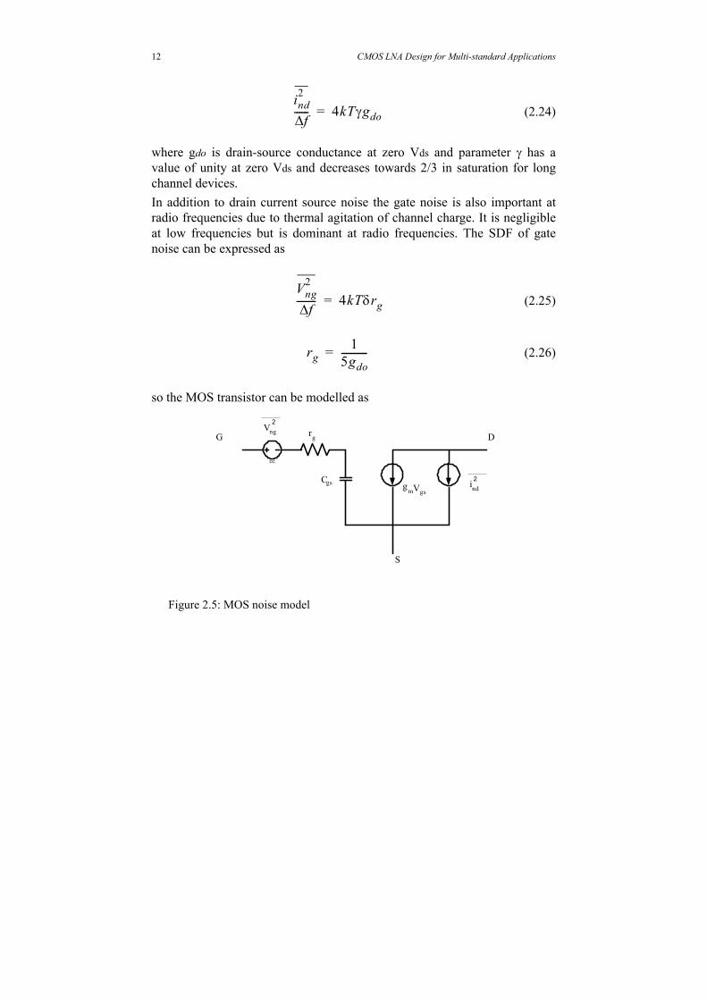
where gdo is drain-source conductance at zero Vds and parameter γ has a value of unity at zero Vds and decreases towards 2/3 in saturation for long channel devices.In addition to drain current source noise the gate noise is also important at radio frequencies due to thermal agitation of channel charge. It is negligible at low frequencies but is dominant at radio frequencies. The SDF of gate noise can be expressed as
(2.25)
(2.26)
so the MOS transistor can be modelled as
Figure 2.5: MOS noise model
ind2
f∆------ 4kTγgdo=
Vng2
f∆-------- 4kTδrg=
rg1
5gdo-----------=
DC
G
S
D
gmVgs
rg
Cgs
Vng2
ind2
13
2.7 RECEIVER ARCHITECTURES.
2.7.1 HETERODYNE RECEIVERS.
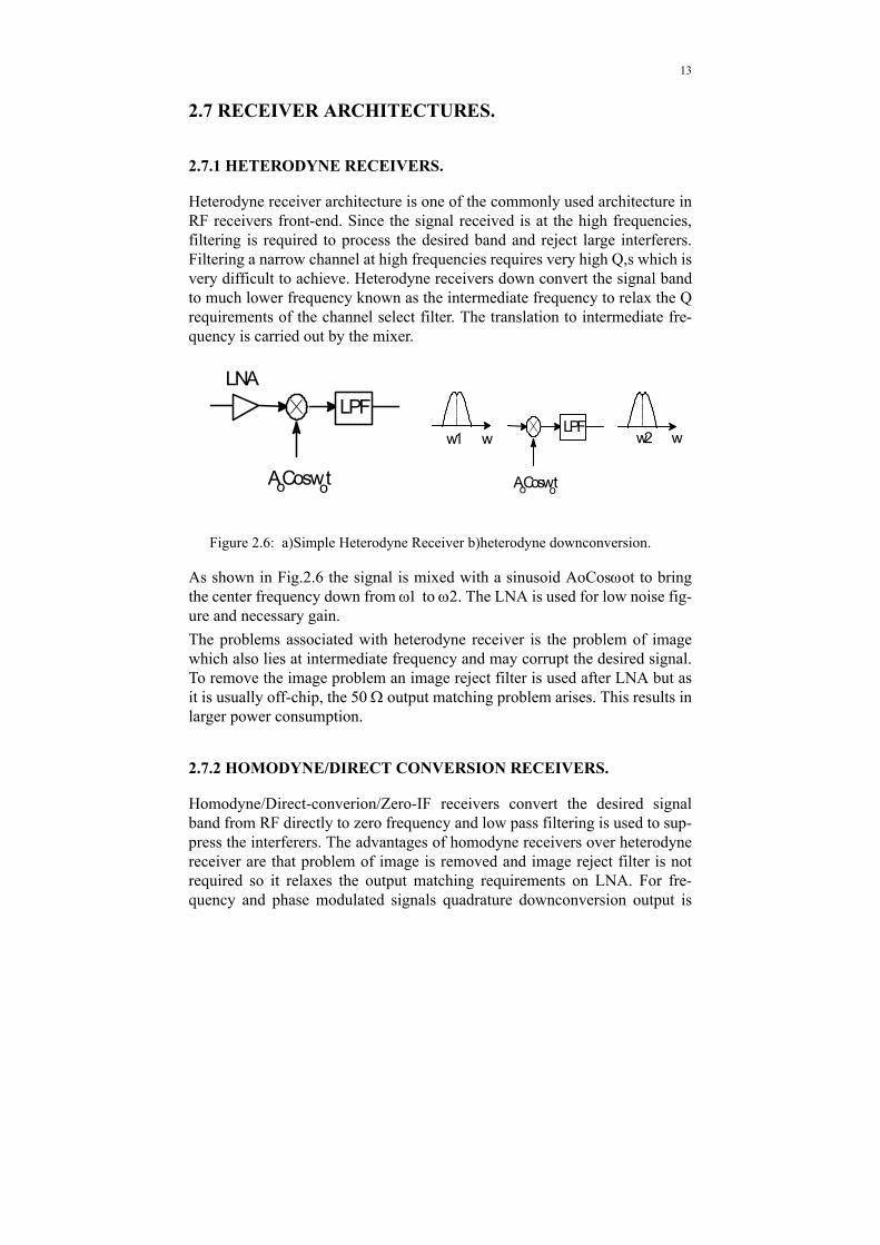
Heterodyne receiver architecture is one of the commonly used architecture in RF receivers front-end. Since the signal received is at the high frequencies, filtering is required to process the desired band and reject large interferers. Filtering a narrow channel at high frequencies requires very high Q,s which is very difficult to achieve. Heterodyne receivers down convert the signal band to much lower frequency known as the intermediate frequency to relax the Q requirements of the channel select filter. The translation to intermediate fre-quency is carried out by the mixer.
As shown in Fig.2.6 the signal is mixed with a sinusoid AoCosωot to bring the center frequency down from ω1 to ω2. The LNA is used for low noise fig-ure and necessary gain.The problems associated with heterodyne receiver is the problem of image which also lies at intermediate frequency and may corrupt the desired signal. To remove the image problem an image reject filter is used after LNA but as it is usually off-chip, the 50 Ω output matching problem arises. This results in larger power consumption.
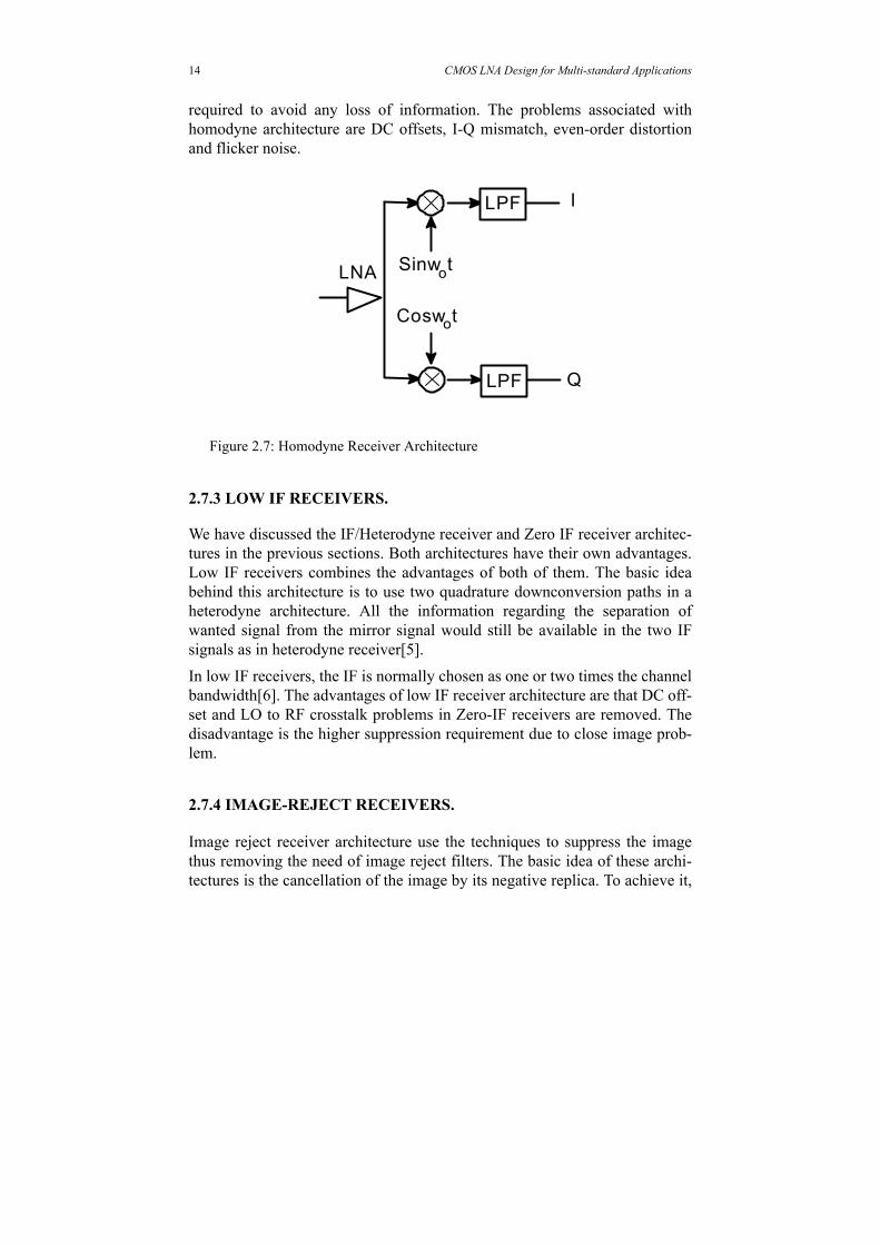
2.7.2 HOMODYNE/DIRECT CONVERSION RECEIVERS.
Homodyne/Direct-converion/Zero-IF receivers convert the desired signal band from RF directly to zero frequency and low pass filtering is used to sup-press the interferers. The advantages of homodyne receivers over heterodyne receiver are that problem of image is removed and image reject filter is not required so it relaxes the output matching requirements on LNA. For fre-quency and phase modulated signals quadrature downconversion output is
A Cosw to o
LPFLNA
A Cosw to o
w1 w w2 wLPF
14 CMOS LNA Design for Multi-standard Applications
required to avoid any loss of information. The problems associated with homodyne architecture are DC offsets, I-Q mismatch, even-order distortion and flicker noise.
Figure 2.7: Homodyne Receiver Architecture
2.7.3 LOW IF RECEIVERS.
We have discussed the IF/Heterodyne receiver and Zero IF receiver architec-tures in the previous sections. Both architectures have their own advantages. Low IF receivers combines the advantages of both of them. The basic idea behind this architecture is to use two quadrature downconversion paths in a heterodyne architecture. All the information regarding the separation of wanted signal from the mirror signal would still be available in the two IF signals as in heterodyne receiver[5]. In low IF receivers, the IF is normally chosen as one or two times the channel bandwidth[6]. The advantages of low IF receiver architecture are that DC off-set and LO to RF crosstalk problems in Zero-IF receivers are removed. The disadvantage is the higher suppression requirement due to close image prob-lem.
2.7.4 IMAGE-REJECT RECEIVERS.
Image reject receiver architecture use the techniques to suppress the image thus removing the need of image reject filters. The basic idea of these archi-tectures is the cancellation of the image by its negative replica. To achieve it,
Cosw t
o
o
LPF
LNA
LPF
Sinw t
I
Q
15
the signal and the image are processed differently as the two lie on different sides of LO frequency.
Hartley Architecture.
In Hartley Architecture the RF signal is mixed with the quadrature phase of local oscillator and after passing it through low pass filter one side is shifted by 90 degree to produce the same polarity for the signal and opposite for image. By adding the two sides image is rejected
Figure 2.8: Hartley Image Reject Architecture
Weaver Architecture.In weaver architecture both sides after passing through low pass filter are again mixed with second local oscillator frequency and then subtracted one from the other to reject the image and get the desired IF signal.
LPF
LPF
RF IFcoswtsinwto
o
90o
16 CMOS LNA Design for Multi-standard Applications
17
3 INDUCTIVE SOURCE DEGENERATED
LNA DESIGN
LNA is the first stage of radio receiver whose main function is to amplify the signal while adding as little noise as possible. The noise figure of LNA is the main factor in overall noise figure of receiver and noise of subsequent stage is suppressed by the factor of gain of LNA as given by Frii,s formula. Inductive source degenerated LNA topology is considered the optimum choice due to its low noise figure and good gain. Design aspects of inductive source degenated LNA are discussed here.
3.1 INPUT MATCHING.
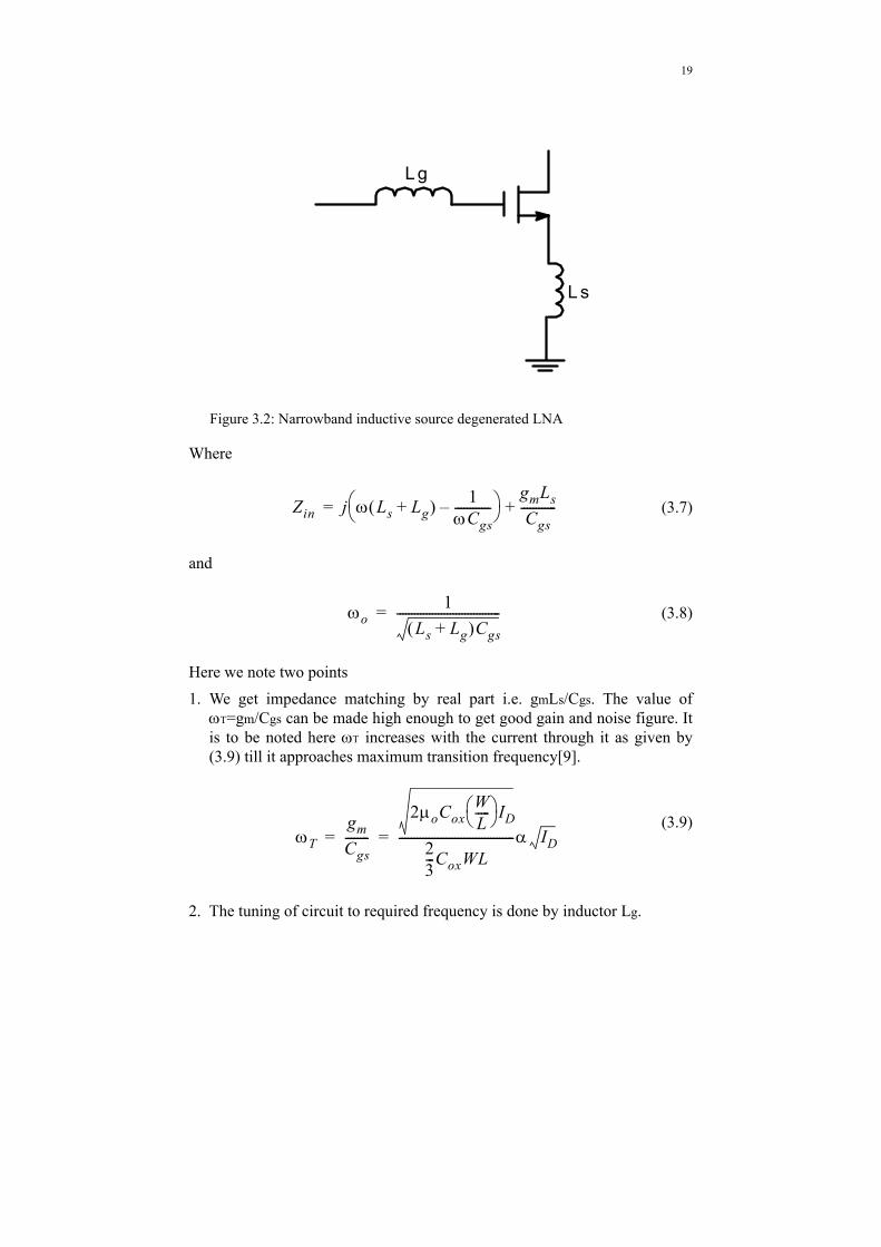
The basic principle of inductive source degenated LNA input matching is shown below
Figure 3.1: a) Inductive source degenerated LNA input stage b)equivalent small signal model
L s
g m Vg sVg sC g s
L s
18 CMOS LNA Design for Multi-standard Applications
Applying a voltage V at input and solving for current I in small signal model gives
(3.1)
where
(3.2)
which gives input impedance as
(3.3)
(3.4)
(3.5)
where
(3.6)
which is unity current gain magnitude frequency. A higher value of unity cur-rent gain frequency (fT) is desirable both for good gain and low noise figure.The imaginary part in (3.14) cancels at frequency of resonance and we get the input matching of 50 ohms from the real part. However to cancel out the imaginary part at the required frequency of resonance we need a large value of Cgs for example for matching at 2.4GHz with Ls of 5nH we need Cgs = 881fF for which we need 829um wide transistor in 0.35um CMOS technol-ogy which is quite large.Also to match to 50ohms gm is 8.8mS. So, an induc-tor is added in series with gate of input transistor to get required resonant frequency. The modified circuit is shown in Fig. 3.2.
Here we note two points1. We get impedance matching by real part i.e. gmLs/Cgs. The value of
ωT=gm/Cgs can be made high enough to get good gain and noise figure. It is to be noted here ωΤ increases with the current through it as given by (3.9) till it approaches maximum transition frequency[9].
(3.9)
2. The tuning of circuit to required frequency is done by inductor Lg.
L s
L g
Zin j ω Ls Lg+( ) 1ωCgs------------–⎝ ⎠
⎛ ⎞ gmLsCgs
------------+=
ωo1
Ls Lg+( )Cgs-----------------------------------=
ωTgmCgs--------
2µoCoxWL-----⎝ ⎠
⎛ ⎞ ID
23---CoxWL
---------------------------------------α ID= =
20 CMOS LNA Design for Multi-standard Applications
3.2 GAIN.
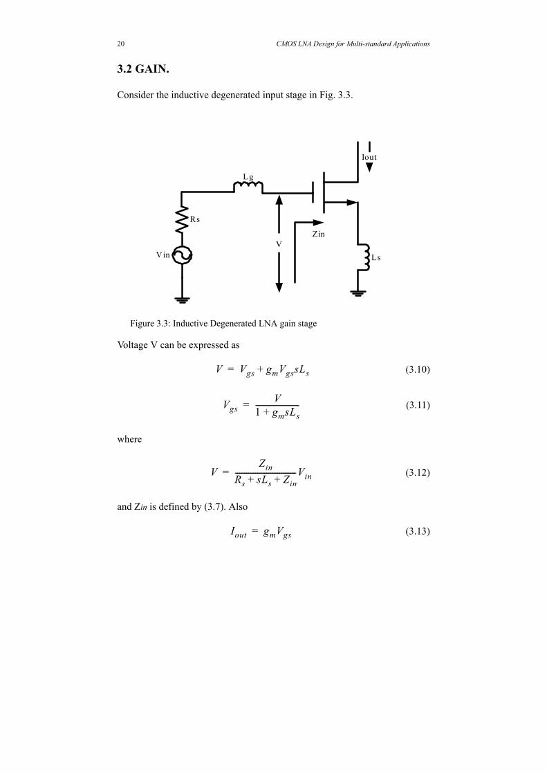
Consider the inductive degenerated input stage in Fig. 3.3.
putting V from (3.12) into (3.14) and putting value of Zin from (3.7) we get
(3.15)
from above equation at resonance
(3.16)
solving for the stage transconductance gain gives
(3.17)
An interesting point to note here is that the transconductance gain of the stage is not dependent on gm of input transistor but is related to its unity current gain frequency fT We will use this result in the analysis of noise figure in next section.
3.3 NOISE FIGURE.
Considering the LNA input stage in Fig. 3.2. There are two noise sources at the input, tunable inductor and input transistor. The noise due to inductor series resistance can be reduced by methods to improve the Q of inductor however Q of on-chip inductor in CMOS is low (normally in the range of 6-10) and adds significantly to noise figure.
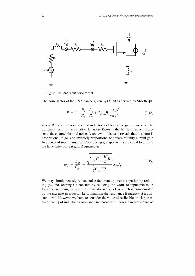
The other noise source at the input of LNA is the input transistor. The noise of input transistor is due to thermal noise of its drain and gate. The equivalent circuit for input stage noise calculation is given in Fig. 3.4
Ioutgm
1 gmsLs+------------------------V=
Iout1 ωTLsCgs LsCgss
2+ +
1 Rs ωTLs+( )sCgs Lg Ls+( )s2Cgs+ +---------------------------------------------------------------------------------------------
22 CMOS LNA Design for Multi-standard Applications
Figure 3.4: LNA input noise Model
The noise factor of the LNA can be given by (3.18) as derived by Shaeffer[8]
(3.18)
where Rl is series resistance of inductor and Rg is the gate resistance.The dominant term in the equation for noise factor is the last term which repre-sents the channel thermal noise. A review of this term reveals that this term is proportional to gdo and inversely proportional to square of unity current gain frequency of input transistor. Considering gdo approximately equal to gm and we have unity current gain frequency as
(3.19)
We may simultaneously reduce noise factor and power dissipation by reduc-ing gdo and keeping ωT constant by reducing the width of input transistor. However reducing the width of transistor reduces Cgs which is compensated by the increase in inductor Lg to maintain the resonance frequency at a con-stant level. However we have to consider the value of realizable on-chip tran-sistor and Q of inductor as resistance increases with increase in inductance as
Ls
Lg
Rs
Vin
Iout
RgRl
i d2
v rg2
vrl2
F 1RlRs-----
RgRs------ ϒgdoRs
ωoωT------⎝ ⎠
⎛ ⎞2
+ + +=
ωTgmCgs--------
2µoCoxWL-----⎝ ⎠
⎛ ⎞ ID
23---CoxWL
---------------------------------------α ID= =
23
larger coil is required and practical on-chip inductor value is limited to around 10nH. Another impact of this strategy is that it tends to degrade the linearity due to increased signal levels across Cgs[8]. The inverse dependence of noise factor on square of unity current gain frequency also shows the as we scale down in technology fT of transistor is increasing so noise figure should improve with scaling down[8].
As we have discussed a narrow device has high fT which improves noise fig-ure but there is also another factor i.e. gate noise which is prominent at nar-row device size and tends to degrade noise figure as discussed in chapter 2 with relation to noise in MOS devices at high frequency.
24 CMOS LNA Design for Multi-standard Applications
25
4 DESIGN OF MULTISTANDARD LNA
4.1 PREVIOUS WORK
The frequency bands of 1.8GHz and 2.4GHz are widely being used in com-munication systems. Frequency band of 1.8GHz is used in DCS1800 and GSM while 2.4GHz frequency band is WLAN 802.11b standards and is also frequency band for Bluetooth. These standards are the most used standards in modern communication systems and there is a great need for transceivers capable of working with both frequency standards. In this chapter we will dis-cuss some previously designed dual band LNAs and then the new design strategy for tunable LNA will be presented.
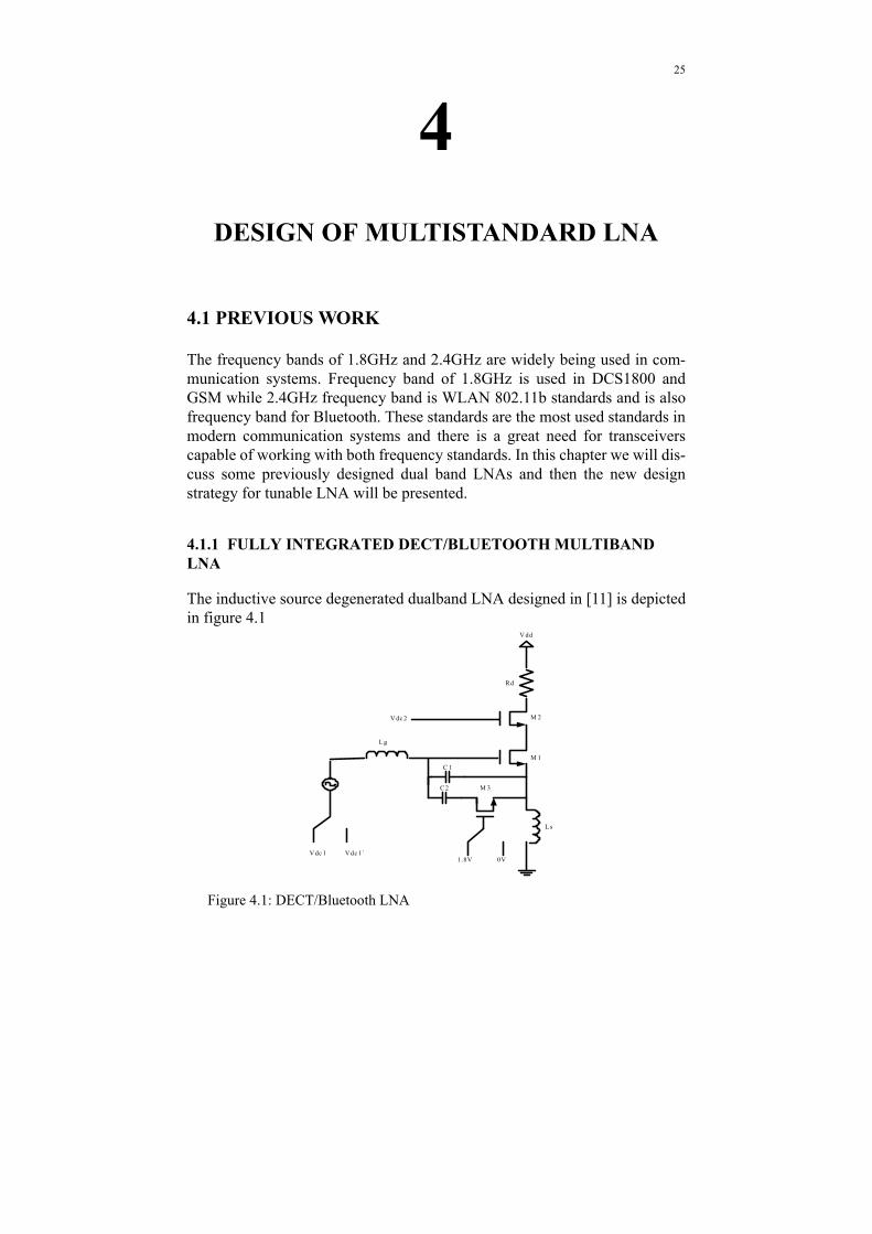
The inductive source degenerated dualband LNA designed in [11] is depicted in figure 4.1
Figure 4.1: DECT/Bluetooth LNA
C 1
C 2
V dc 2
Lg
Ls
V dc 1 Vdc 1´1.8V 0V
M 1
M 2
M 3
V dd
Rd
26 CMOS LNA Design for Multi-standard Applications
In this LNA frequency tuning is done by capacitors C1 and C2.When switch M3 is turned on, capacitor C2 is added in parallel with Cgs and operating fre-quency is lowered. If we derive the input impedance its expression is
(4.1)
where
(4.2)
We see here that as we make Cgs(eff) larger to tune LNA to lower frequency the effective real part ´decreases so to keep the input impedance matching gmhas to be increased which has been done by increasing the current through LNA. While it is an effective way to tune between two frequency bands, the power consumption is not the same for both standards.
4.1.2 CONCURRENT DUALBAND LNA
The concurrent dualband LNA presented in [12] is designed for WLAN 802.11a/b standards and is given in Fig. 4.2.
Figure 4.2: Concurrent dualband LNA
Zin j ω Ls Lg+( ) 1ωCgs eff( )---------------------–⎝ ⎠
⎛ ⎞ gmLsCgs eff( )-----------------+=
Cgs eff( ) Cgs C1 C2+ +=
27
In this LNA the input matching for two frequency bands has been achieved by off chip parallel LC circuit and bond wire inductance by using the two tones of resonant circuit. This LNA performs operation at 2.4GHz and 5.5GHz and also there are off-chip components.
4.1.3 A COMPACT 2.4/5.2GHZ CMOS DUALBAND LOW NOISE AMPLIFIER.
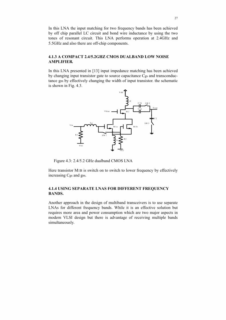
In this LNA presented in [13] input impedance matching has been achieved by changing input transistor gate to source capacitance Cgs and transconduc-tance gm by effectively changing the width of input transistor. the schematic is shown in Fig. 4.3.
Figure 4.3: 2.4/5.2 GHz dualband CMOS LNA
Here transistor M1B is switch on to switch to lower frequency by effectively increasing Cgs and gm.
4.1.4 USING SEPARATE LNAS FOR DIFFERENT FREQUENCY BANDS.
Another approach in the design of multiband transceivers is to use separate LNAs for different frequency bands. While it is an effective solution but requires more area and power consumption which are two major aspects in modern VLSI design but there is advantage of receiving multiple bands simultaneously.
Ld
Ls
c
C 1b
C 1 a
C 2
V dd
c
R 1
R 2
V bias
V b 1
V b 2
V inM 1 a M 1b
M 2
S W 1
S W 2
S W 3Lg
V o ut
28 CMOS LNA Design for Multi-standard Applications
4.2 INDUCTIVE SOURCE DEGENERATED TUNABLE LNA
In this thesis work an inductive source degenated low noise amplifier has been designed for the frequency bands of 1.8GHz and 2.4GHz. Inductive source degeration topology has been selected as it presents best noise figure in a narrowband frequency of interest. Design strategy for multiband function is discussed here.
4.2.1 INPUT MATCHING WITH TUNABILITY
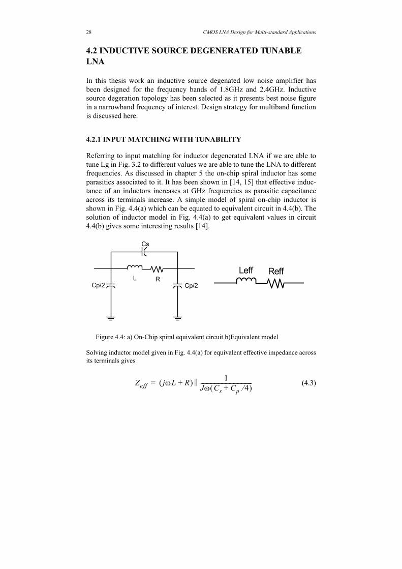
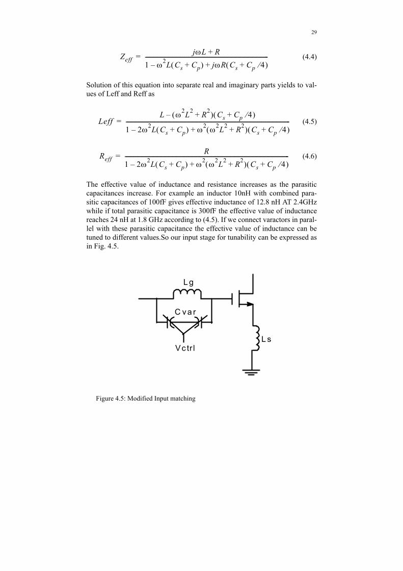
Referring to input matching for inductor degenerated LNA if we are able to tune Lg in Fig. 3.2 to different values we are able to tune the LNA to different frequencies. As discussed in chapter 5 the on-chip spiral inductor has some parasitics associated to it. It has been shown in [14, 15] that effective induc-tance of an inductors increases at GHz frequencies as parasitic capacitance across its terminals increase. A simple model of spiral on-chip inductor is shown in Fig. 4.4(a) which can be equated to equivalent circuit in 4.4(b). The solution of inductor model in Fig. 4.4(a) to get equivalent values in circuit 4.4(b) gives some interesting results [14].
Figure 4.4: a) On-Chip spiral equivalent circuit b)Equivalent model
Solving inductor model given in Fig. 4.4(a) for equivalent effective impedance across its terminals gives
Solution of this equation into separate real and imaginary parts yields to val-ues of Leff and Reff as
(4.5)
(4.6)
The effective value of inductance and resistance increases as the parasitic capacitances increase. For example an inductor 10nH with combined para-sitic capacitances of 100fF gives effective inductance of 12.8 nH AT 2.4GHz while if total parasitic capacitance is 300fF the effective value of inductance reaches 24 nH at 1.8 GHz according to (4.5). If we connect varactors in paral-lel with these parasitic capacitance the effective value of inductance can be tuned to different values.So our input stage for tunability can be expressed as in Fig. 4.5.
30 CMOS LNA Design for Multi-standard Applications
The choice and implementation of varactors will be discussed later in next section.
4.2.2 VARACTOR DESIGN.
There are two type of varactors commonly used, diode varactor and MOS varactor. In both cases the devices are placed in separate wells and well potential is used as the tuning voltage, so commonly used devices for varactor design are therefore pn diode and PMOS [18].
The reverse bias diode varactors have been commonly used but they suffer due to the low quality factor Q and thus would be an additional noise source at the input of LNA so they has not been considered to be used in this design. MOS varactors have been used in designing of various circuits like VCOs[16]. The commonly used device is PMOS either in inversion mode or accumulation mode known as inversion-mode MOS capacitor and accumula-tion mode MOS capacitors respectively. Both type of MOS varactors are briefly discussed here.
MOS VARACTORS.
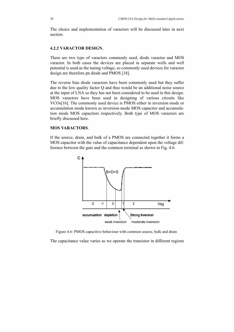
If the source, drain, and bulk of a PMOS are connected together it forms a MOS capacitor with the value of capacitance dependent upon the voltage dif-ference between the gate and the common terminal as shown in Fig. 4.6.
Figure 4.6: PMOS capacitive behaviour with common source, bulk and drain
The capacitance value varies as we operate the transistor in different regions
accumulation depletion Strong Inversion
B=D=S
Vsg
CC
-2 -1 0 1 2
accumulation depletion Strong Inversion
weak inversion moderate inversion
31
on both sides of value of Vsg.
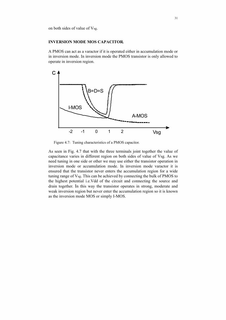
INVERSION MODE MOS CAPACITOR.
A PMOS can act as a varactor if it is operated either in accumulation mode or in inversion mode. In inversion mode the PMOS transistor is only allowed to operate in inversion region.
Figure 4.7: Tuning characteristics of a PMOS capacitor.
As seen in Fig. 4.7 that with the three terminals joint together the value of capacitance varies in different region on both sides of value of Vsg. As we need tuning in one side or other we may use either the transistor operation in inversion mode or accumulation mode. In inversion mode varactor it is ensured that the transistor never enters the accumulation region for a wide tuning range of Vsg. This can be achieved by connecting the bulk of PMOS to the highest potential i.e.Vdd of the circuit and connecting the source and drain together. In this way the transistor operates in strong, moderate and weak inversion region but never enter the accumulation region so it is known as the inversion mode MOS or simply I-MOS.
I-MOS
A-MOS
B=D=S
Vsg
CC
-2 -1 0 1 2
32 CMOS LNA Design for Multi-standard Applications
Figure 4.8: Inversion-Mode MOS Capacitor
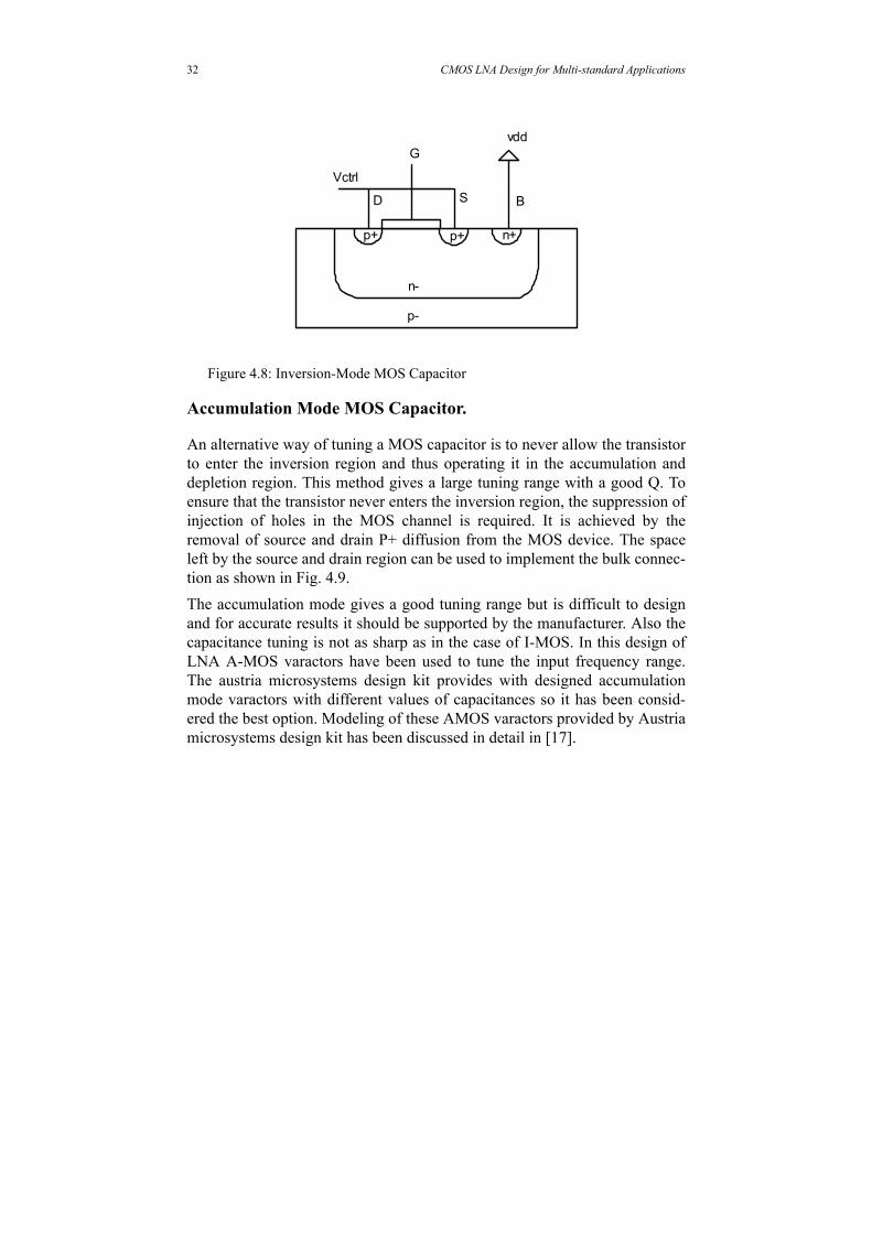
Accumulation Mode MOS Capacitor.
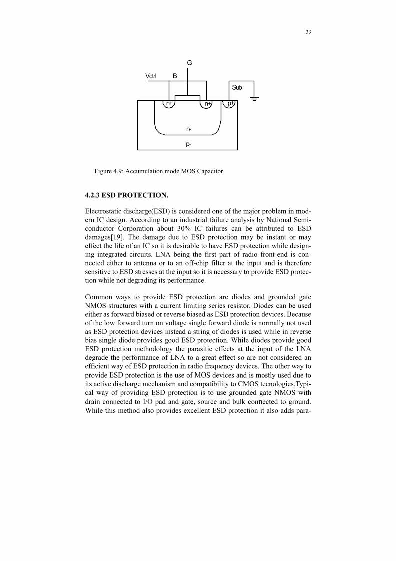
An alternative way of tuning a MOS capacitor is to never allow the transistor to enter the inversion region and thus operating it in the accumulation and depletion region. This method gives a large tuning range with a good Q. To ensure that the transistor never enters the inversion region, the suppression of injection of holes in the MOS channel is required. It is achieved by the removal of source and drain P+ diffusion from the MOS device. The space left by the source and drain region can be used to implement the bulk connec-tion as shown in Fig. 4.9.The accumulation mode gives a good tuning range but is difficult to design and for accurate results it should be supported by the manufacturer. Also the capacitance tuning is not as sharp as in the case of I-MOS. In this design of LNA A-MOS varactors have been used to tune the input frequency range. The austria microsystems design kit provides with designed accumulation mode varactors with different values of capacitances so it has been consid-ered the best option. Modeling of these AMOS varactors provided by Austria microsystems design kit has been discussed in detail in [17].
n-
p-
p+ n+
G
B
p+
SD
vdd
Vctrl
33
Figure 4.9: Accumulation mode MOS Capacitor
4.2.3 ESD PROTECTION.
Electrostatic discharge(ESD) is considered one of the major problem in mod-ern IC design. According to an industrial failure analysis by National Semi-conductor Corporation about 30% IC failures can be attributed to ESD damages[19]. The damage due to ESD protection may be instant or may effect the life of an IC so it is desirable to have ESD protection while design-ing integrated circuits. LNA being the first part of radio front-end is con-nected either to antenna or to an off-chip filter at the input and is therefore sensitive to ESD stresses at the input so it is necessary to provide ESD protec-tion while not degrading its performance.
Common ways to provide ESD protection are diodes and grounded gate NMOS structures with a current limiting series resistor. Diodes can be used either as forward biased or reverse biased as ESD protection devices. Because of the low forward turn on voltage single forward diode is normally not used as ESD protection devices instead a string of diodes is used while in reverse bias single diode provides good ESD protection. While diodes provide good ESD protection methodology the parasitic effects at the input of the LNA degrade the performance of LNA to a great effect so are not considered an efficient way of ESD protection in radio frequency devices. The other way to provide ESD protection is the use of MOS devices and is mostly used due to its active discharge mechanism and compatibility to CMOS tecnologies.Typi-cal way of providing ESD protection is to use grounded gate NMOS with drain connected to I/O pad and gate, source and bulk connected to ground. While this method also provides excellent ESD protection it also adds para-
n-
p-
n+ n+
G
Vctrl B
p+
Sub
34 CMOS LNA Design for Multi-standard Applications
sitics at the input of LNA which is undesirable and may degrade the perfor-mance of LNA.
One common way to provide ESD protection in LNA as proposed by many researchers is the use of inductors [20, 21]. The ESD currents occur normally at low frequency compared to RF signal so any device which acts as low pass filter can be used and inductor is the device with such characteristics [20]. In addition to providing ESD protection inductor also tunes out the parasitic capacitance due to pad, line etc. at the operating frequency thus improving its performance.
From ESD protection point of view, the on-resistance of inductor determines the voltage across it so an inductor with small on-resistance is preferable to limit the voltage at the gate of transistor. Moreover it should provide large resistance to ground at RF frequency. As it is discussed that if inductor forms parallel resonant circuit with parasitic capacitance it is desired to act as a bandstop filter at the required RF frequency. An inductor with self resonance frequency close to desired frequency band would therefore be a good option. At resonance the equivalent parasitic resistance of ESD inductor is given by [21]
(4.7)
where Resd is parasitic series resistance, if this parallel resistance at required frequency band is very large compared to Rs, this would have no effect at the input and classical source degeneration matching theory holds. The noise contribution of this ESD protection is estimated as[21]
(4.8)
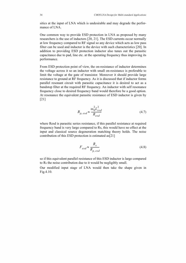
so if this equivalent parallel resistance of this ESD inductor is large compared to Rs the noise contribution due to it would be negligibly small.Our modified input stage of LNA would then take the shape given in Fig.4.10.
Rp esd,ω0
2Lesd2
Resd-----------------≈
FesdRs
Rp esd,--------------≈
35
Figure 4.10: ESD protected input stage of LNA
where Cpar represents the parasitic capacitance of pad and wires and Lesd is the ESD protection inductor.
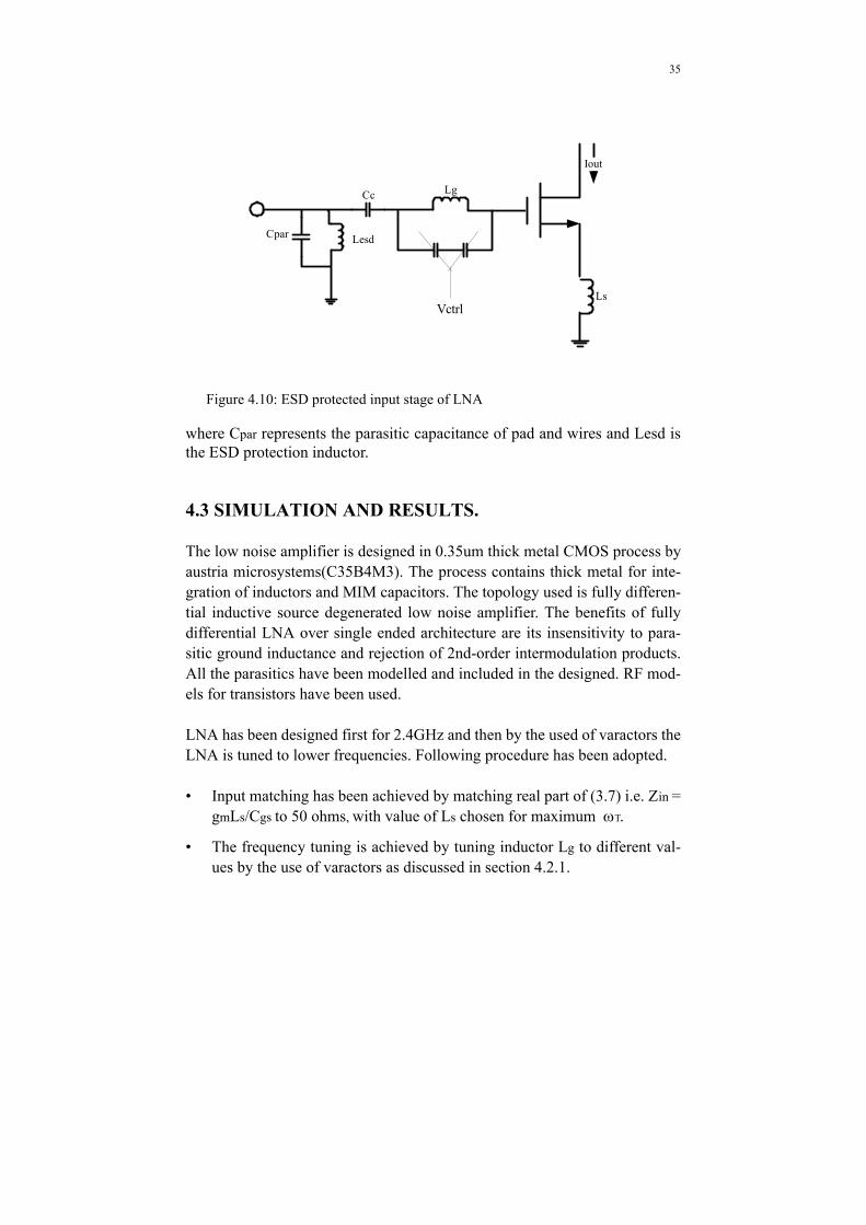
4.3 SIMULATION AND RESULTS.
The low noise amplifier is designed in 0.35um thick metal CMOS process by austria microsystems(C35B4M3). The process contains thick metal for inte-gration of inductors and MIM capacitors. The topology used is fully differen-tial inductive source degenerated low noise amplifier. The benefits of fully differential LNA over single ended architecture are its insensitivity to para-sitic ground inductance and rejection of 2nd-order intermodulation products. All the parasitics have been modelled and included in the designed. RF mod-els for transistors have been used.
LNA has been designed first for 2.4GHz and then by the used of varactors the LNA is tuned to lower frequencies. Following procedure has been adopted.
• Input matching has been achieved by matching real part of (3.7) i.e. Zin = gmLs/Cgs to 50 ohms, with value of Ls chosen for maximum ωT.
• The frequency tuning is achieved by tuning inductor Lg to different val-ues by the use of varactors as discussed in section 4.2.1.
Ls
Lg
Iout
Cc
Vctrl
LesdCpar
36 CMOS LNA Design for Multi-standard Applications
• Transistor sizing has been done for minimum noise figure and acceptable gain. It has been considered to have a realizable on-chip inductance value for inductor Lg i.e. not more than 10nH.
The fully differential LNA designed is shown in figure 4.11.
Figure 4.11: Fully differential Tunable LNA
Values of different components are first derived from mathematical formulas for 2.4GHz frequency. The optimum width of the input transistors can be determined by (4.9) derived for power constrained noise optimization in [1]
(4.9)
For 2.4GHz frequency with L =0.35um and for 50ohms input resistance, we get optimal width of input transistor as
(4.10)
as we know that
inp inn
outpoutn
VDD
Vbias
Vctrl Vctrl
M1 M2
M3 M4
Ld Ld
Lg Lg
CvarCvar
LsLs
Lesd Lesd
Wopt1
3ωLCoxRs--------------------------=
Wopt 274um=
37
(4.11)
For 0.35um CMOS process we have
(4.12)
plugging values of Cox, W and L in (4.11) we get the value of Cgs as
(4.13)
which gives
(4.14)
Now we may calculate the value of source degenerated inductor and gate inductor from (3.8)
(4.15)
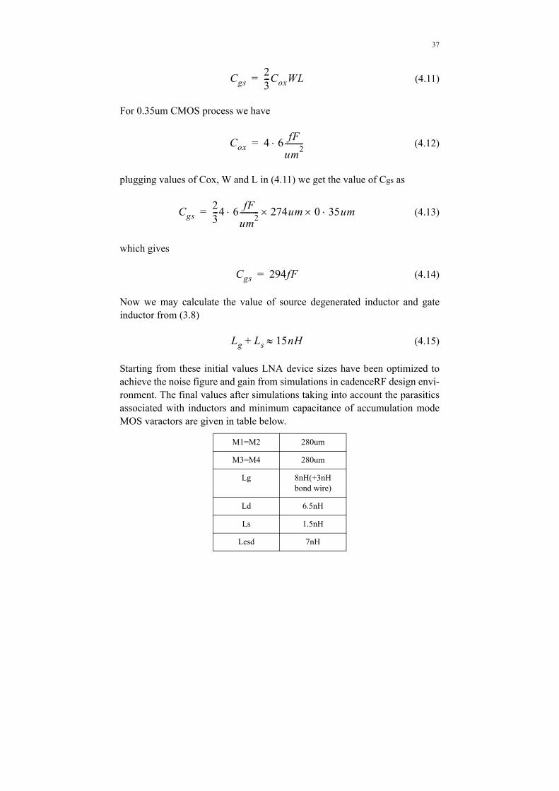
Starting from these initial values LNA device sizes have been optimized to achieve the noise figure and gain from simulations in cadenceRF design envi-ronment. The final values after simulations taking into account the parasitics associated with inductors and minimum capacitance of accumulation mode MOS varactors are given in table below.
M1=M2 280um
M3=M4 280um
Lg 8nH(+3nH bond wire)
Ld 6.5nH
Ls 1.5nH
Lesd 7nH
Cgs23---CoxWL=
Cox 4 6 fFum2----------⋅=
Cgs23---4 6 fF
um2---------- 274um 0 35um⋅××⋅=
Cgs 294fF=
Lg Ls 15nH≈+
38 CMOS LNA Design for Multi-standard Applications
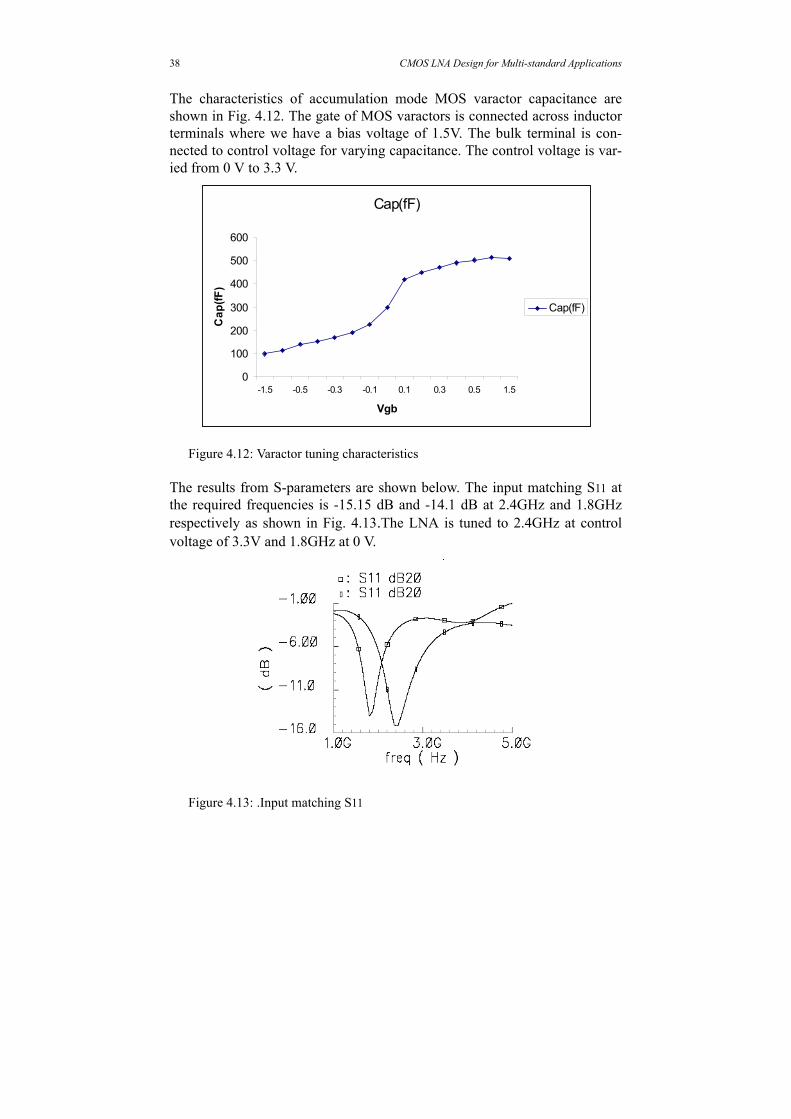
The characteristics of accumulation mode MOS varactor capacitance are shown in Fig. 4.12. The gate of MOS varactors is connected across inductor terminals where we have a bias voltage of 1.5V. The bulk terminal is con-nected to control voltage for varying capacitance. The control voltage is var-ied from 0 V to 3.3 V.
Figure 4.12: Varactor tuning characteristics
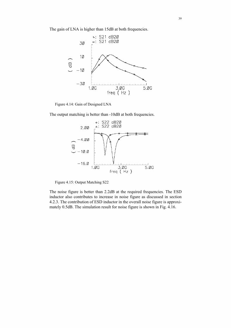
The results from S-parameters are shown below. The input matching S11 at the required frequencies is -15.15 dB and -14.1 dB at 2.4GHz and 1.8GHz respectively as shown in Fig. 4.13.The LNA is tuned to 2.4GHz at control voltage of 3.3V and 1.8GHz at 0 V.
Figure 4.13: .Input matching S11
Cap(fF)
0
100
200
300
400
500
600
-1.5 -0.5 -0.3 -0.1 0.1 0.3 0.5 1.5
Vgb
Cap(fF)
Cap(fF)
39
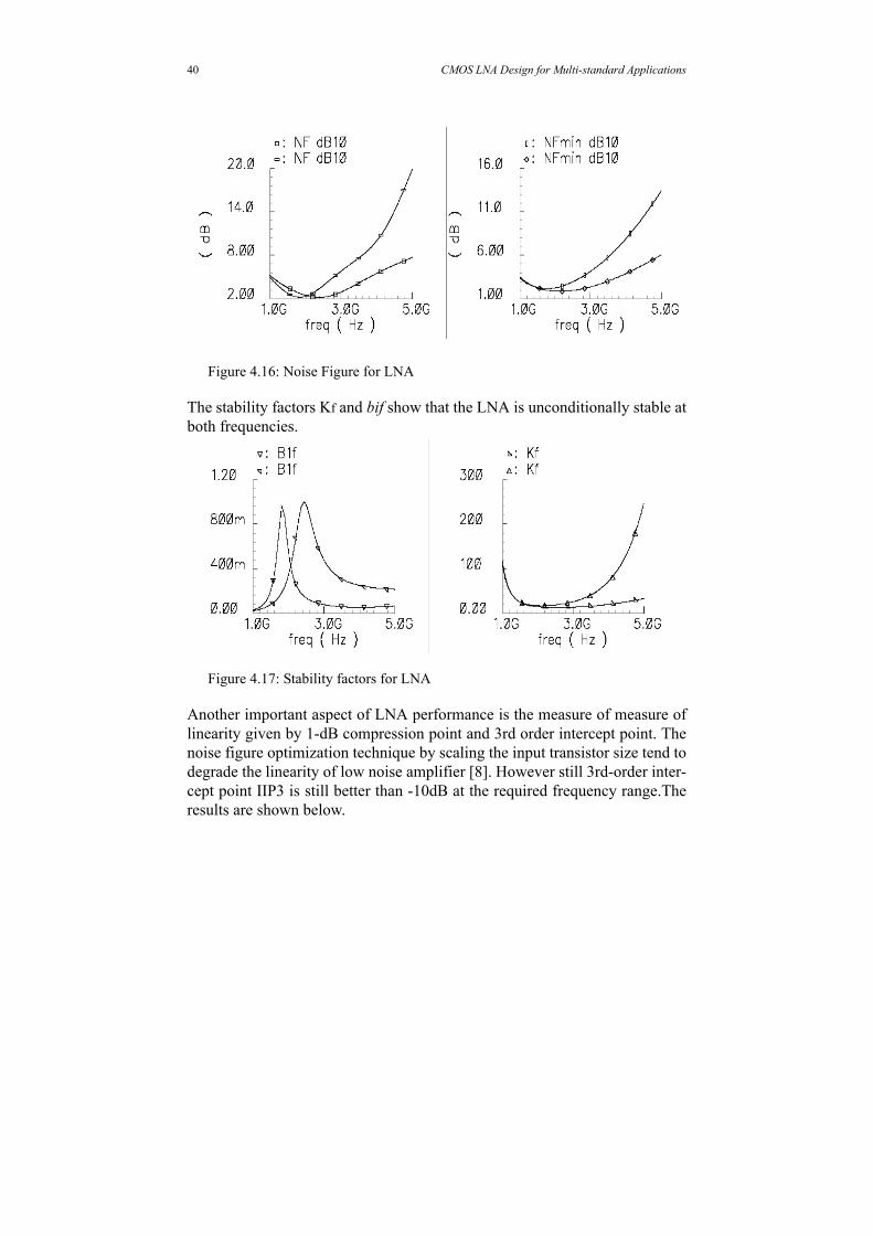
The gain of LNA is higher than 15dB at both frequencies.
Figure 4.14: Gain of Designed LNA
The output matching is better than -10dB at both frequencies.
Figure 4.15: Output Matching S22
The noise figure is better than 2.2dB at the required frequencies. The ESD inductor also contributes to increase in noise figure as discussed in section 4.2.3. The contribution of ESD inductor in the overall noise figure is approxi-mately 0.5dB. The simulation result for noise figure is shown in Fig. 4.16.
40 CMOS LNA Design for Multi-standard Applications
Figure 4.16: Noise Figure for LNA
The stability factors Kf and bif show that the LNA is unconditionally stable at both frequencies.
Figure 4.17: Stability factors for LNA
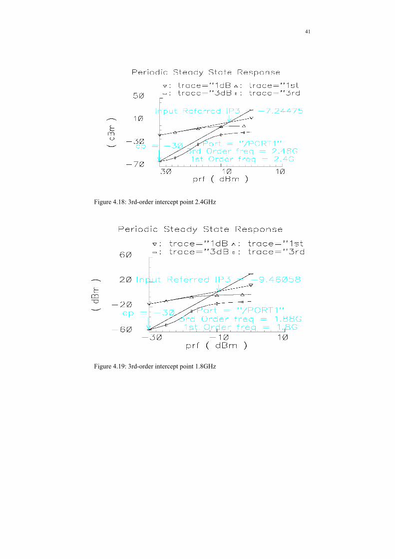
Another important aspect of LNA performance is the measure of measure of linearity given by 1-dB compression point and 3rd order intercept point. The noise figure optimization technique by scaling the input transistor size tend to degrade the linearity of low noise amplifier [8]. However still 3rd-order inter-cept point IIP3 is still better than -10dB at the required frequency range.The results are shown below.
41
Figure 4.18: 3rd-order intercept point 2.4GHz
Figure 4.19: 3rd-order intercept point 1.8GHz
42 CMOS LNA Design for Multi-standard Applications
Figure 4.20: 1-DB Compression point 2.4GHz
Figure 4.21: 1-dB Compression point 1.8GHz
43
4.3.1 ESD PROTECTION RESULTS.
ESD protection at the gate of input transistor was simulated by applying a current of 1.34A(2KV HBM standard) at the input of LNA with a sharp rise time of <10nS and a slow fall time as shown below. The voltage at the gate of input transistor is limited to 5V which is the breakdown limit. The results are shown below.
Figure 4.22: ESD Protection Simulation results.
44 CMOS LNA Design for Multi-standard Applications
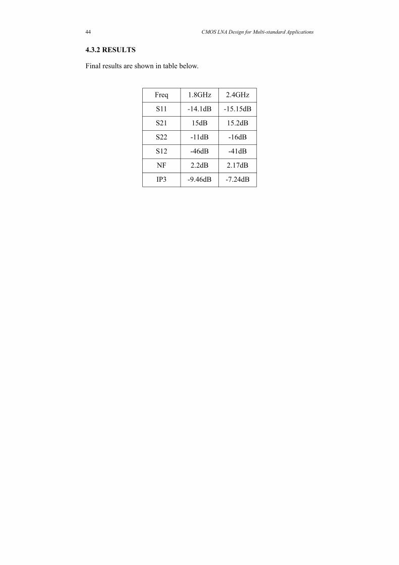
4.3.2 RESULTS
Final results are shown in table below.
Freq 1.8GHz 2.4GHz
S11 -14.1dB -15.15dB
S21 15dB 15.2dB
S22 -11dB -16dB
S12 -46dB -41dB
NF 2.2dB 2.17dB
IP3 -9.46dB -7.24dB
45
5 DESIGN, MODELLING AND LAYOUT
OF INDUCTORS
5.1 INTRODUCTION.
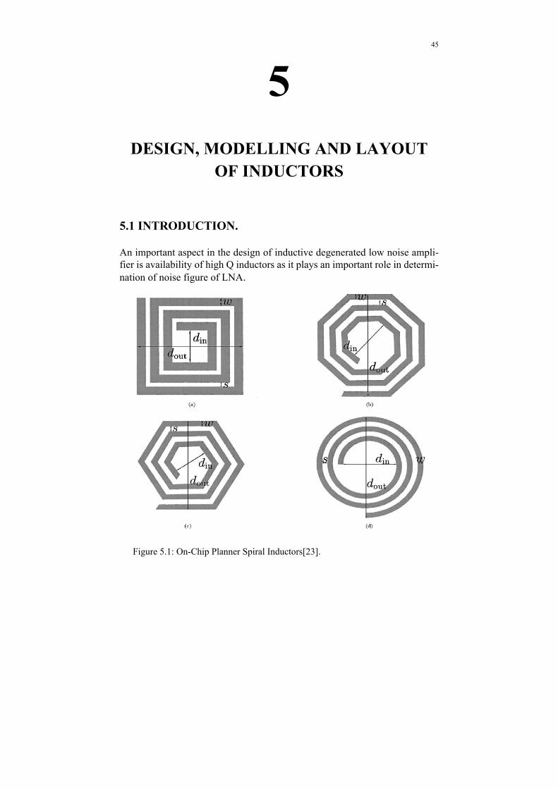
An important aspect in the design of inductive degenerated low noise ampli-fier is availability of high Q inductors as it plays an important role in determi-nation of noise figure of LNA.
Figure 5.1: On-Chip Planner Spiral Inductors[23].
46 CMOS LNA Design for Multi-standard Applications
Planner spirals are most commonly used as on-chip inductors. These induc-tors are constructed in the top metal layer of CMOS process due to its maxi-mum distance from the substrate which results in low parasitic capacitance between inductor and substrate. Also most IC processes provide the thick top metal layer for layout of inductors. The Q factor of such inductors depends upon the conductivity of metal layer and other parasitic components which would be discussed in this chapter. Planner spirals can be of different shapes i.e. square, hexagonal, octagonal and circular as shown in Fig. 5.1.
The choice of inductor shape normally depends upon the availability of lay-out tool for a particular shape. Rectangular/square spirals are the most widely used spirals due to easy layout and commonly available tools, however octag-onal and circular spirals exhibit a little better performance the range of 10% than square spirals[1]
5.2 MODELLING OF A SPIRAL INDUCTOR.
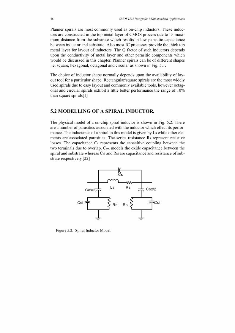
The physical model of a on-chip spiral inductor is shown in Fig. 5.2. There are a number of parasitics associated with the inductor which effect its perfor-mance. The inductance of a spiral in this model is given by Ls while other ele-ments are associated parasitics. The series resistance Rs represent resistive losses. The capacitance Cs represents the capacitive coupling between the two terminals due to overlap. Cox models the oxide capacitance between the spiral and substrate whereas Csi and Rsi are capacitance and resistance of sub-strate respectively.[22]
Figure 5.2: Spiral Inductor Model.
Cs
Ls Rs
Rsi Rsi
Cox/2 Cox/2
Csi Csi
47
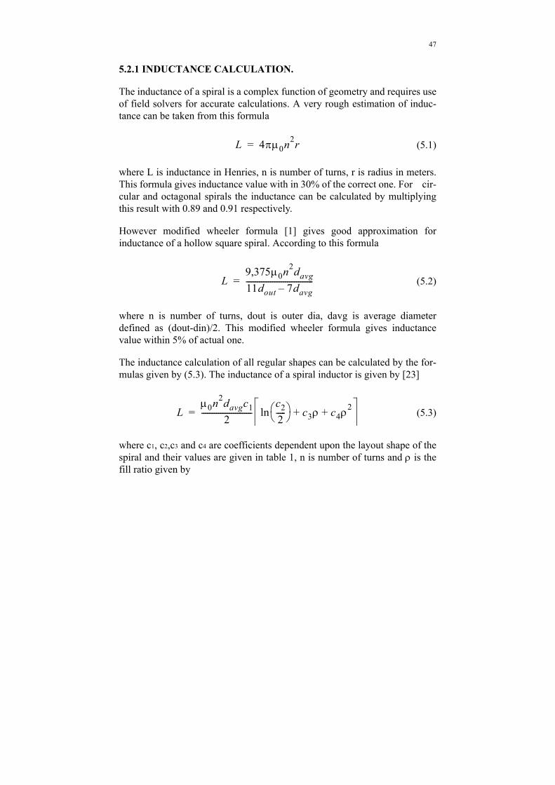
5.2.1 INDUCTANCE CALCULATION.
The inductance of a spiral is a complex function of geometry and requires use of field solvers for accurate calculations. A very rough estimation of induc-tance can be taken from this formula
(5.1)
where L is inductance in Henries, n is number of turns, r is radius in meters. This formula gives inductance value with in 30% of the correct one. For cir-cular and octagonal spirals the inductance can be calculated by multiplying this result with 0.89 and 0.91 respectively.
However modified wheeler formula [1] gives good approximation for inductance of a hollow square spiral. According to this formula
(5.2)
where n is number of turns, dout is outer dia, davg is average diameter defined as (dout-din)/2. This modified wheeler formula gives inductance value within 5% of actual one.
The inductance calculation of all regular shapes can be calculated by the for-mulas given by (5.3). The inductance of a spiral inductor is given by [23]
(5.3)
where c1, c2,c3 and c4 are coefficients dependent upon the layout shape of the spiral and their values are given in table 1, n is number of turns and ρ is the fill ratio given by
48 CMOS LNA Design for Multi-standard Applications
(5.4)
We see from these formulas that thickness of the metal layer presents little or no role in the inductance of spiral however it is important to have thick metal layer to have good Q as thick metal offers low resistance.
5.2.2 SERIES RESISTANCE
The series resistance Rs of a spiral inductor can be estimated by the formula
(5.5)
where l is length of winding, w is width, t is thickness, σ is conductivity of the material and δ is skin depth given by
(5.6)
The resistance of a metal also increases due to the skin effect at high frequen-cies. Skin effect may be defined as the tendency of the current to flow on the skin of the metal at high frequency thereby effectively reducing the width and increasing resistance.
wσδ 1 e t δ⁄––( )-------------------------------------=
δ 2wσµ0--------------=
49
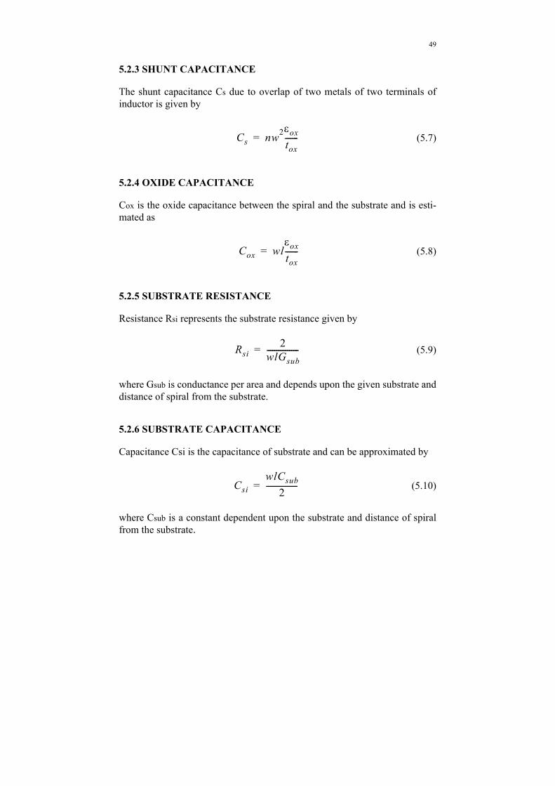
5.2.3 SHUNT CAPACITANCE
The shunt capacitance Cs due to overlap of two metals of two terminals of inductor is given by
(5.7)
5.2.4 OXIDE CAPACITANCE
Cox is the oxide capacitance between the spiral and the substrate and is esti-mated as
(5.8)
5.2.5 SUBSTRATE RESISTANCE
Resistance Rsi represents the substrate resistance given by
(5.9)
where Gsub is conductance per area and depends upon the given substrate and distance of spiral from the substrate.
5.2.6 SUBSTRATE CAPACITANCE
Capacitance Csi is the capacitance of substrate and can be approximated by
(5.10)
where Csub is a constant dependent upon the substrate and distance of spiral from the substrate.
Cs nw2εoxtox-------=
Cox wlεoxtox-------=
Rsi2
wlGsub-----------------=
CsiwlCsub
2-----------------=
50 CMOS LNA Design for Multi-standard Applications
5.3 METHODS TO IMPROVE Q OF INDUCTORS.
With the above mentioned model we may optimize Q of the inductor keeping in view the operation frequency. One common method is to use hollow induc-tor as innermost turns of a spiral contribute negligibly to total flux but they contribute to overall loss thus minimizing Q.
Pattern ground shield has been described as an efficient method to increase the Q of inductor as it prevents coupling to lossy substrate thus effectively reducing the effect of the substrate terms Csi and Rsi. It also reduces the cou-pling of noise from the substrate to inductor and vice versa. The pattern ground shield is usually constructed with the polysilicon with slots. One neg-ative aspect of pattern ground shield is that it results in reduction of self reso-nant frequency due to the increased capacitance [24]
Another method is to place alternating wedges of n-well and substrate under the inductor to minimize the eddy currents. Magnetic current of the inductor induces eddy currents in the substrate which result in losses due to conductive silicon substrate. Eddy currents flow in opposite direction and thus reduce the electromagnetic field. A solution to this problem as presented by Stein-mair[26] is to create isolation barriers in the p-substrate by placing n-well structures and limiting eddy currents within small area. The eddy current den-sity increases with increasing the radius of an inductor so denser n-well would result in stronger isolation effect. Applying supply voltage to n-well further enhances the effect and results in further increase in quality factor and self resonant frequency [27].
5.4 INDUCTOR DESIGN USING ASITIC.
ASITIC is the inductance modelling and design tool used in this thesis for design and layout of inductors. The detailed description of ASITIC is pro-vided in [25]. The accuracy of designed inductors depends upon the process technology file which one has to write for a particular process. The technol-ogy file describes the substrate and metal layer of the process. The automati-cally generated layout in the form of a CIF file can be imported to cadence.The process used in this work is 0.35um thick metal CMOS by austria microsystems. It is described in Fig.5.3 [26].
51
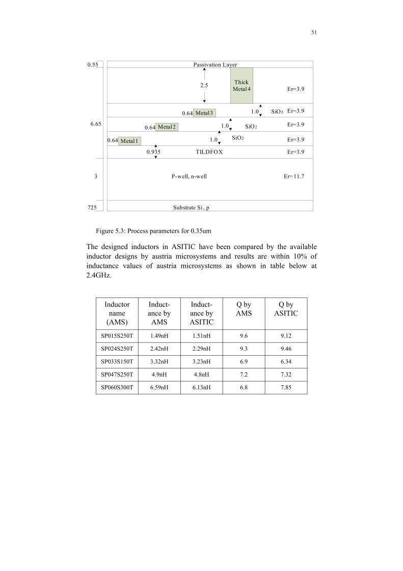
Figure 5.3: Process parameters for 0.35um
The designed inductors in ASITIC have been compared by the availableinductor designs by austria microsystems and results are within 10% of inductance values of austria microsystems as shown in table below at 2.4GHz.
Inductorname
(AMS)
Induct-ance by AMS
Induct-ance by ASITIC
Q by AMS
Q by ASITIC
SP015S250T 1.49nH 1.51nH 9.6 9.12
SP024S250T 2.42nH 2.29nH 9.3 9.46
SP033S150T 3.32nH 3.23nH 6.9 6.34
SP047S250T 4.9nH 4.8nH 7.2 7.32
SP060S300T 6.59nH 6.13nH 6.8 7.85
Metal1
Metal2
Metal3
ThickMetal 4
725
3
6.65
0.55
Substrate Si , p
P-well, n-well
TILDFOX0.935
0.64
0.64
0.64
SiO2
SiO2
SiO2
Er=11.7
Er=3.9
Er=3.9
Er=3.9
Er=3.9
Er=3.9
1.0
1.0
1.0
2.5
Passivation Layer
52 CMOS LNA Design for Multi-standard Applications
5.5 DESIGNED INDUCTORS.
In this work we designed two inductors needed in layout of LNA. The design aspects and value calculation is given below. The most important consider-ation of the designs are to have high Q while having a sufficient high self res-onant frequency. As we are operating in the frequency range of 1.8GHz to 2.4 GHz, it has been considered that the self resonating frequency of the inductor should be at least in the range of 4GHz or above. We may increase the width of metal to reduce the series resistance of inductor keeping in view the self resonant frequency. Following is the design procedure.• Circular spirals has been designed due to slightly better Q than square
spirals.
• The width of metal wire is < 10um as wider metal results in low self res-onant frequency due to increased substrate capacitance which is undesira-ble.
• For high Q hollow spiral layout is done. Also alternating wedges of n-well and substrate have been placed underneath the inductor to improve Q. Pattern ground shield has not been employed due to its effect on self resonant frequency.
Figure 5.4: a) 8 nH inductor b) 6.5 nH inductor
the inductors were designed using inductor modelling and layout tool ASITIC and then imported to cadence environment for simulation and layout.
The inductance value of inductor (a) provided by asitic is 8.02nH, with parameters wire width w=9um, spacing s= 3um,number of turns n=5,outer
53
dia dout=290um and inner diameter din= 161um. By using (5.3) we get inductance value of 7.59nH.
Inductor b has design parameters w=9um, s=3um, n=4.5, dout=270um and din=153um. the value of inductance calculated by asitic and (5.3) are respec-tively 6.4nH and 5.95nH. The values attained from asitic has been used in simulations of LNA with inductor model given in Fig. 5.2. The inductance value has been cross checked with above formulas. The values of parasitics has been included while simulating.
54 CMOS LNA Design for Multi-standard Applications
55
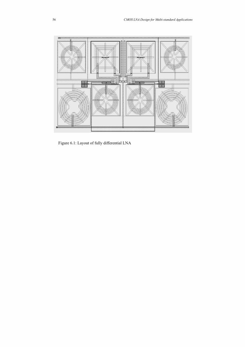
6 LAYOUT ISSUES
The layout of fully differential Low noise amplifier has been carried out in 0.35um CMOS Austria microsystems thick metal module. The layout of RF integrated circuits plays an important role in proper circuit functioning of a chip.The parasitics of wires for routing of signals degrade the performance of ICs and need to be minimized by proper layout. Following points were con-sidering while doing the layout of LNA.
• Fully symmetrical layout has been carried out for the fully differential LNA.
• Thick metal layer Metal4 has been used for realization of on-chip induc-tors and routing of input and output signals due to its low resistivity and maximum distance from the substrate which results in low parasitic capacitance.
• Guard rings have been placed around the inductors and sensitive circuitry to provide effective isolation and to reduce noise coupling. Large guard rings have been placed around inductors for isolation.
• It is recommended that multiple ground pads and bond wires should be used as ground of IC and PCB ground will not be at same potential due to inductance of bond wires. The effect can be minimized by using multiple bond wires and pad connected in parallel.
The layout of the designed fully differential low noise amplifiers given in Fig. 6.1.
56 CMOS LNA Design for Multi-standard Applications
Figure 6.1: Layout of fully differential LNA
57
7 CONCLUSION AND FUTURE WORK
7.1 CONCLUSION
In this thesis a new input matching topology for tunable narrowband LNAs has been discussed and a fully differential tunable LNA has been designed in 0.35um AMS process. The design has been validated through Cadence Spec-treRF simulation tool. The simulations show good results for the frequency range 1.8GHz to 2.4GHz. The tunability to frequencies in between 1.8GHz and 2.4GHz is limited due to sharp change in varactor capacitance from the accumulation to depletion mode. However at 1.8GHz and 2.4GHz the LNA provides stable operation with varactors operating fully in accumulation and depletion modes respectively.
ESD protection for RF circuits is also discussed in this thesis. The common ESD protection techniques using diodes and gate grounded transistor degrade the performance of LNA due to capacitive coupling of signal to ground. The use of inductor as ESD protection element at input of LNA not only tunes out the parasitics at the input due to pad and bond wires, it also provides excellent ESD protection. This design of LNA also includes ESD protection at the input of LNA.
As this LNA has all passive elements on-chip so on-chip spiral inductor mod-elling is discussed and circular spiral inductors are designed using ASITIC and used in this LNA.
Post layout simulations were not possible due to unavailability of inductance extraction however all parasitics were estimated through available documen-tation and included in the design.
58 CMOS LNA Design for Multi-standard Applications
7.2 FUTURE WORK
For verification the layout needs to be extracted with all parasitics and manu-factured. Also further study can be performed on inductance extraction of the designed inductors.
59
REFERENCES
[1] Thomas H. Lee “The Design of CMOS Radio-Frequency Integrated Circuits” 2nd Edition, Cambridge University Press, 2004.
[3] Rein Ludwig, Paulo Bretchko “RF Circuit Design: Theory and Applications” Prentice Hall 2000.
[4] Bosco H. Leung “VLSI for Wireless Communication” Prentice Hall, 2002.
[5] Crols, J. Steyeart, M.S.J. “Low-IF topologies for high-performance analog front ends of fully integrated receivers” IEEE Transactions on Circuits and Systems-II: Analog and Digital Signal Processing vol.45; No.3 March 1998.
[6] Mirabbasi S., Martin K. “Classical and modern receiver architectures” IEEE Communication Magazine November 2000.
[7] Razavi B. “Architectures and circuits for RF CMOS receivers” IEEE Custom Integrated Circuit Conference 1998
[8] Shaeffer, D.K. Lee, T.H. “A 1.5-V, 1.5-GHz CMOS low noise amplifier” IEEE Journal of Solid-State Circuits vol.32 May 1997
[9] Gatta, F. Sacchi, E. Svelto, F. Vilmercati, P. Castello, R. “A 2-dB noise figure 900-MHz differential CMOS LNA” IEEE Journal of Solid-State Circuits October 2001
[10] Andreani, P. Sjoland, H. “Noise optimization of an inductively degenerated CMOS low noise amplifier” IEEE transactions on Circuits and Systems II: Analog and Digital Signal Processing September 2001
[11] Vidojkovic, V. van der Tang, J. Hanssen, E. Leeuwenburgh, A. van Roermund, A. “Fully-integrated DECT/Bluetooth multi-band LNA in 0.18 /spl mu/m CMOS” ISCAS 2004.
[12] Hashemi, H. Hajimiri, A. “Concurrent multiband low-noise amplifiers-theory, design, and applications” IEEE Transactions on Microwave Theory and Tech-niques, January 2002.
[13] Liang-Hung Lu, Hsieh-Hung Hsieh, Yu-Shun Wang “A compact 2.4/5.2-GHz CMOS dual-band low-noise amplifier” IEEE Microwave and Wireless Letters October 2005.
[14] Xiaomin Yang, Thomas X. Wu, John McMacken “Design of LNA at 2.4GHz
60 CMOS LNA Design for Multi-standard Applications
using 0.25um CMOS technology” Microwave and Optical Technology Letters February 2003.
[15] Mou Shouxian, Ma Jian-Guo, Yeo Kiat Seng, Do Manh Anh “A modified architecture used for input matching in CMOS low-noise amplifiers” IEEE Transactions on Circuits and Systems November 2005.
[16] Andreani, P. Mattisson, S. “On the use of MOS varactors in RF VCOs” IEEE Journal of Solid-State Circuits, June 2002.
[17] Molner, K. Rappitsch, G. Huszka, Z. Seebacher, E. “MOS varactor modeling with a subcircuit utilizing the BSIM3v3 model” IEEE Transactions on Elec-tronic Devices July 2002.
[18] Porret, A.S. Melly, T. Enz, C.C. Vittoz, E.A. “Design of high-Q varactors for low-power wireless applications using a standard CMOS process” IEEE Jour-nal of Solid-State Circuits March 2002.
[19] Wang, Albert, Z.H. “On-chip ESD protection for Integrated Circuits, An IC Design Perspective” Kluwer Academic Publishers 2002.
[20] Leroux, P. Steyaert, M. “High-performance 5.2 GHz LNA with on-chip induc-tor to provide ESD protection” Electronics Letters, March 2001.
[21] Linten, D. Thijs, S. Natarajan, M.I. Wambacq, P. Jeamsaksiri, W. Ramos, J. Mercha, A. Jenei, S. Donney, S. Decoutere, S. “A 5-GHz fully integrated ESD-protected low-noise amplifier in 90-nm RF CMOS” IEEE Journal of Solid-State Circuits July 2005.
[22] Yue, C.P. Wong, S.S. “Physical modeling of spiral inductors on silicon” IEEE Transactions on Electronics Devices March 2002.
[23] Mohan, S.S. del Mar Hershenson, M. Boyd,S.P. Lee, T.H. “Simple accurate expressions for planar spiral inductances” IEEE Journal of Solid-State Cir-cuits October 1999.
[24] Yue, C.P. Wong, S.S “On-chip spiral inductors with patterned ground shields for Si-based RF ICs” IEEE Journal of Solid State Circuits May 1998.
[25] Ali M. Niknejad, Robert G. Meyer “Design, Simulation and application of inductors and Transformers for Si RF ICs” Kluwer Academic Publishers 2000.
[26] Steinmaier, A. Mayer, M.L. Molnar, K. Ribic, N. Huszka, Z. Seebacher, E. Magerl, G. “Improvement of Differential Planar Spiral Inductors on a 0.35/spl mu/m BiCMOS Process” European Microwave Conference June 2005
[27] Maget, J. Kraus, R. Tiebout, M. “Voltage-controlled Substrate Structure for Integrated Inductors in Standard Digital CMOS Technologies” IEEE Solid State Devices Research Conference September 2002
[28] Martin, K. Johns, D.A. “Analog Integrated Circuit Design”. John Wiley & Sons Inc. 1997.
På svenska
Detta dokument hålls tillgängligt på Internet – eller dess framtida ersättare – under en längre tid från publiceringsdatum under förutsättning att inga extra-ordinära omständigheter uppstår.
Tillgång till dokumentet innebär tillstånd för var och en att läsa, ladda ner, skriva ut enstaka kopior för enskilt bruk och att använda det oförändrat för ickekommersiell forskning och för undervisning. Överföring av upphovsrätten vid en senare tidpunkt kan inte upphäva detta tillstånd. All annan användning av dokumentet kräver upphovsmannens medgivande. För att garantera äktheten, säkerheten och tillgängligheten finns det lösningar av teknisk och administrativ art.
Upphovsmannens ideella rätt innefattar rätt att bli nämnd som upphovsman i den omfattning som god sed kräver vid användning av dokumentet på ovan beskrivna sätt samt skydd mot att dokumentet ändras eller presenteras i sådan form eller i sådant sammanhang som är kränkande för upphovsmannens litterära eller konstnärliga anseende eller egenart.
För ytterligare information om Linköping University Electronic Press se förlagets hemsida http://www.ep.liu.se/
In English
The publishers will keep this document online on the Internet - or its possible replacement - for a considerable time from the date of publication barring exceptional circumstances.
The online availability of the document implies a permanent permission for anyone to read, to download, to print out single copies for your own use and to use it unchanged for any non-commercial research and educational purpose. Subsequent transfers of copyright cannot revoke this permission. All other uses of the document are conditional on the consent of the copyright owner. The publisher has taken technical and administrative measures to assure authenticity, security and accessibility.
According to intellectual property law the author has the right to be mentioned when his/her work is accessed as described above and to be protected against infringement.
For additional information about the Linköping University Electronic Press and its procedures for publication and for assurance of document integrity, please refer to its WWW home page: http://www.ep.liu.se/