Page 1
CMOS VLSI DESIGN
ROCHESTER INSTITUTE OF TECHNOLOGYMICROELECTRONIC ENGINEERING
CMOS VLSI DESIGN
Dr. Lynn FullerWebpage: http://people.rit.edu/~lffeee
Microelectronic Engineering
© December 26, 2011 Dr. Lynn Fuller
Rochester Institute of Technology
Microelectronic Engineering
Page 1
Microelectronic EngineeringRochester Institute of Technology
82 Lomb Memorial DriveRochester, NY 14623-5604
Tel (585) 475-2035Fax (585) 475-5041
Email: [email protected] webpage: http://www.microe.rit.edu
12-26-2010 cmosvlsi2011.ppt
Page 2
CMOS VLSI DESIGN
OUTLINE
Design ApproachProcess TechnologyMOSIS Design RulesPrimitive Cells, Basic Cells, Macro CellsProjectsMaskmaking
© December 26, 2011 Dr. Lynn Fuller
Rochester Institute of Technology
Microelectronic Engineering
Page 2
MaskmakingReferencesHomework
Page 3
CMOS VLSI DESIGN
THE NEED FOR CAD
With millions of transistors per chip it is impossible todesign with no errors without computers to
© December 26, 2011 Dr. Lynn Fuller
Rochester Institute of Technology
Microelectronic Engineering
Page 3
design with no errors without computers to check layout, circuit performance, process design, etc.
Page 4
CMOS VLSI DESIGN
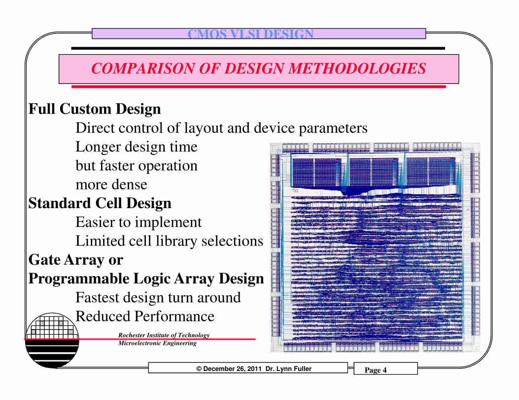
COMPARISON OF DESIGN METHODOLOGIES
Full Custom Design
Direct control of layout and device parametersLonger design timebut faster operationmore dense
Standard Cell Design
© December 26, 2011 Dr. Lynn Fuller
Rochester Institute of Technology
Microelectronic Engineering
Page 4
Standard Cell Design
Easier to implementLimited cell library selections
Gate Array or
Programmable Logic Array Design
Fastest design turn aroundReduced Performance
Page 5
CMOS VLSI DESIGN
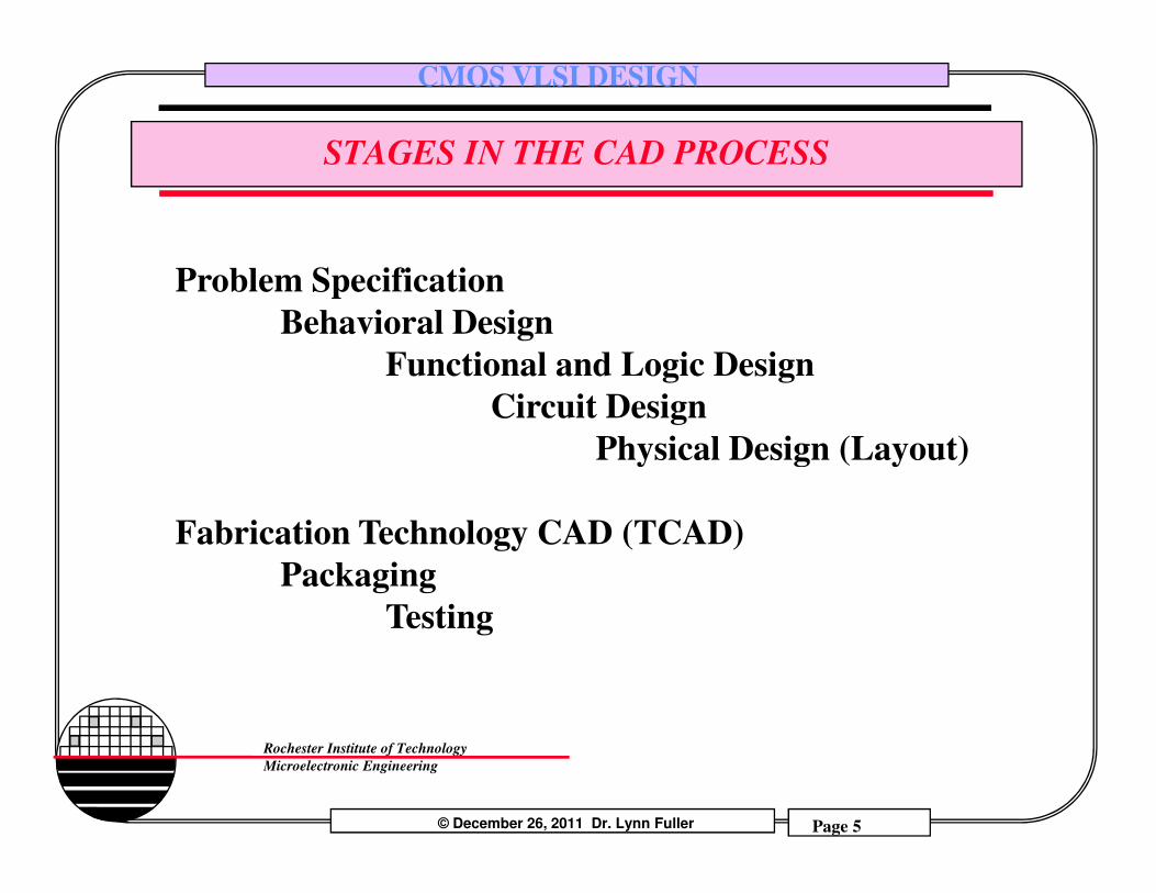
STAGES IN THE CAD PROCESS
Problem Specification
Behavioral Design
Functional and Logic Design
Circuit Design
Physical Design (Layout)
© December 26, 2011 Dr. Lynn Fuller
Rochester Institute of Technology
Microelectronic Engineering
Page 5
Physical Design (Layout)
Fabrication Technology CAD (TCAD)
Packaging
Testing
Page 6
CMOS VLSI DESIGN
DESIGN HEIRARCHY - LEVELS OF ABSTRACTION
A = B + C
if (A) then X: = Y
Block-Functional Model
Gate-Level Model
ALU
Behavioral Model
RAM
© December 26, 2011 Dr. Lynn Fuller
Rochester Institute of Technology
Microelectronic Engineering
Page 6
Gate-Level Model
Transistor level Model
Geometric Model
Page 7
CMOS VLSI DESIGN
PROCESS SELECTION
It is not necessary to know all process details to do CMOS integrated circuit design. However the process determines important circuit parameters such as supply voltage and maximum frequency of operation. It also determines if devices other than PMOS and NMOS transistors can be realized such as poly-to-poly capacitors and EEPROM transistors. The number of metal interconnect layers is also part of the process definition.
© December 26, 2011 Dr. Lynn Fuller
Rochester Institute of Technology
Microelectronic Engineering
Page 7
capacitors and EEPROM transistors. The number of metal interconnect layers is also part of the process definition.
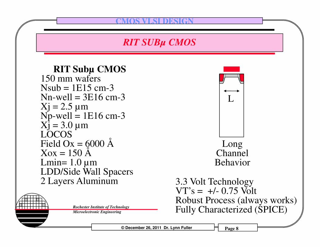
Page 8
CMOS VLSI DESIGN
RIT SUBµ CMOS
RIT Subµ CMOS150 mm wafersNsub = 1E15 cm-3Nn-well = 3E16 cm-3Xj = 2.5 µmNp-well = 1E16 cm-3Xj = 3.0 µm
L
© December 26, 2011 Dr. Lynn Fuller
Rochester Institute of Technology
Microelectronic Engineering
Page 8
Xj = 3.0 µmLOCOSField Ox = 6000 Å Xox = 150 ÅLmin= 1.0 µmLDD/Side Wall Spacers2 Layers Aluminum
LongChannelBehavior
3.3 Volt TechnologyVT’s = +/- 0.75 VoltRobust Process (always works)Fully Characterized (SPICE)
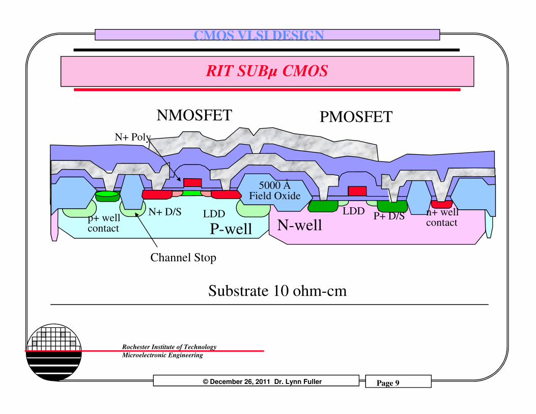
Page 9
CMOS VLSI DESIGN
RIT SUBµ CMOS
5000 ÅField Oxide
NMOSFET PMOSFETN+ Poly
N+ D/S LDD n+ well
© December 26, 2011 Dr. Lynn Fuller
Rochester Institute of Technology
Microelectronic Engineering
Page 9
Substrate 10 ohm-cm
P-well N-wellP+ D/SN+ D/S LDD LDD n+ well
contactp+ wellcontact
Channel Stop
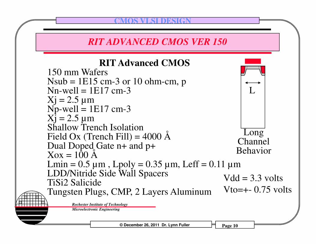
Page 10
CMOS VLSI DESIGN
RIT ADVANCED CMOS VER 150
RIT Advanced CMOS150 mm WafersNsub = 1E15 cm-3 or 10 ohm-cm, pNn-well = 1E17 cm-3Xj = 2.5 µmNp-well = 1E17 cm-3Xj = 2.5 µmShallow Trench Isolation
L
© December 26, 2011 Dr. Lynn Fuller
Rochester Institute of Technology
Microelectronic Engineering
Page 10
Xj = 2.5 µmShallow Trench IsolationField Ox (Trench Fill) = 4000 Å Dual Doped Gate n+ and p+Xox = 100 ÅLmin = 0.5 µm , Lpoly = 0.35 µm, Leff = 0.11 µmLDD/Nitride Side Wall SpacersTiSi2 SalicideTungsten Plugs, CMP, 2 Layers Aluminum
LongChannelBehavior
Vdd = 3.3 voltsVto=+- 0.75 volts
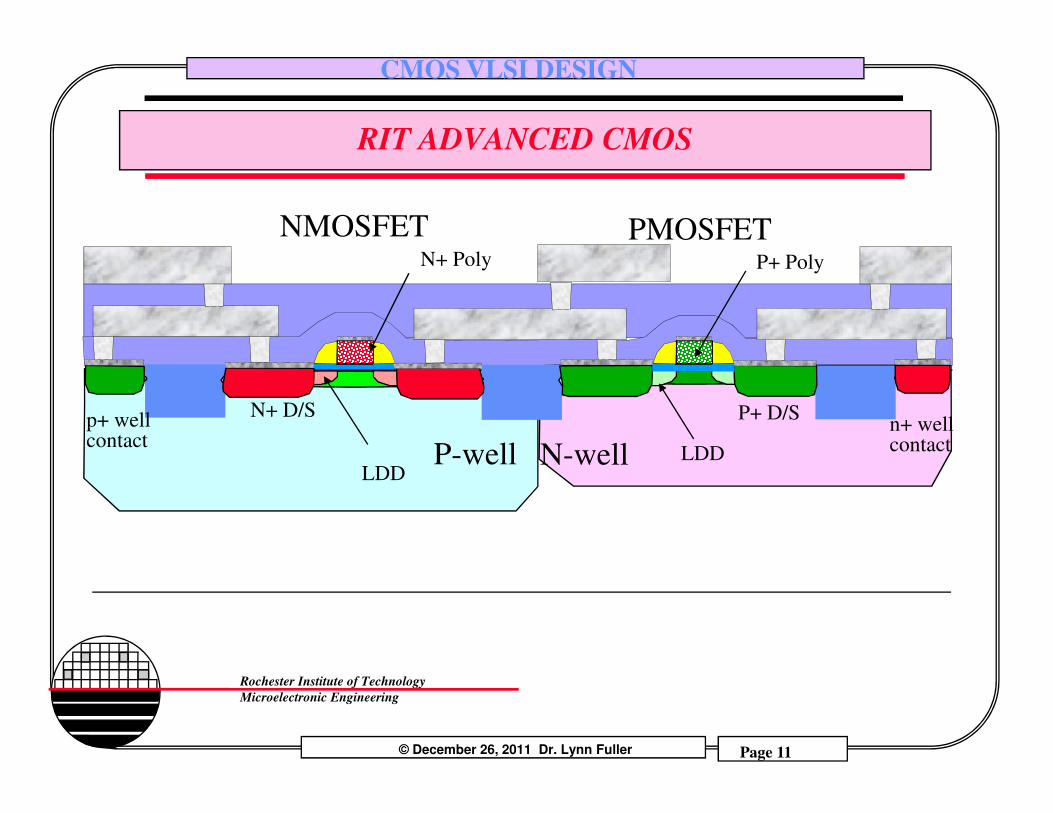
Page 11
CMOS VLSI DESIGN
RIT ADVANCED CMOS
NMOSFET PMOSFETN+ Poly
P+ D/SN+ D/S
P+ Poly
© December 26, 2011 Dr. Lynn Fuller
Rochester Institute of Technology
Microelectronic Engineering
Page 11
N-wellP-wellP+ D/SN+ D/S
LDDLDD
n+ wellcontact
p+ wellcontact
Page 12
CMOS VLSI DESIGN
LAMBDA, Lmin, Ldrawn, Lmask, Lpoly, Lint, Leff, L
Source at 0 VGate
LdrawnLmaskLpoly
Lmin = min drawn poly length, 2λ
Lresist after photo (resist trimming??)
Lmask = ? Depends on +/-bias
Lpoly after poly reoxidation
0.50µm
1.00µm x 5
0.50µm
0.35µmLpoly after poly etch 0.40µm
Lambda = design rule parameter, λ, ie 0.25µm
© December 26, 2011 Dr. Lynn Fuller
Rochester Institute of Technology
Microelectronic Engineering
Page 12
LeffL
Drain at 3.3V
Internal Channel Length, Lint =distance between junctions, including under diffusionEffective Channel Length, Leff = distance between space charge layers,Vd = Vs= 0Channel Length, L, = distance between space charge layers, when Vd= what it isExtracted Channel Length Parameters = anything that makes the fit good (not real)
Lint0.30µm
0.20µm
0.11µmLdrawn = what was drawn
Page 13
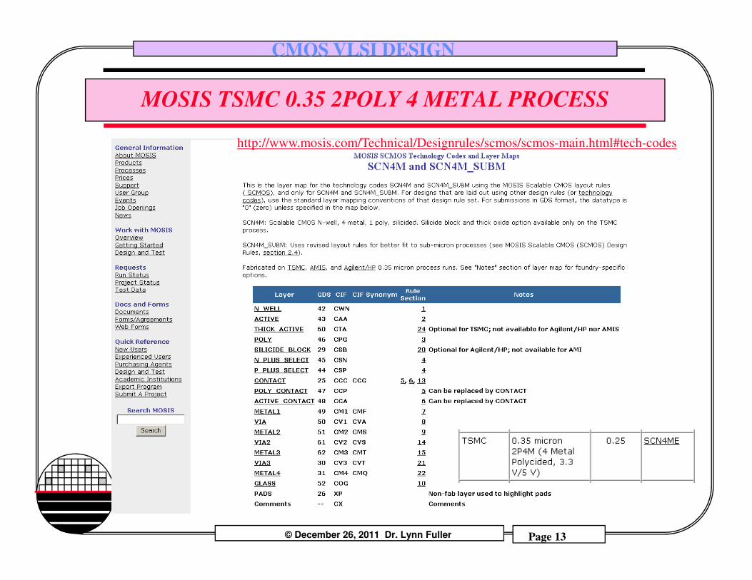
CMOS VLSI DESIGN
MOSIS TSMC 0.35 2POLY 4 METAL PROCESS
http://www.mosis.com/Technical/Designrules/scmos/scmos-main.html#tech-codes
© December 26, 2011 Dr. Lynn Fuller
Rochester Institute of Technology
Microelectronic Engineering
Page 13
Page 14
CMOS VLSI DESIGN
MOSIS TSMC 0.35 2-POLY 4-METAL LAYERS
MASK LAYER NAME
MENTOR NAME
GDS #
COMMENT
N WELL N_well.i 42
ACTIVE Active.i 43
POLY Poly.i 46
N PLUS N_plus_select.i 45
© December 26, 2011 Dr. Lynn Fuller
Rochester Institute of Technology
Microelectronic Engineering
Page 14
N PLUS N_plus_select.i 45
P PLUS P_plus_select.i 44
CONTACT Contact.i 25 Active_contact.i 48
poly_contact.i 47
METAL1 Metal1.i 49
VIA Via.i 50
METAL2 Metal2.i 51
Page 15
CMOS VLSI DESIGN
MORE LAYERS USED IN MASK MAKING
LAYER NAME GDS COMMENT
cell_outline.i 70 Not used
alignment 81 Placed on first level mask
nw_res 82 Placed on nwell level mask
active_lettering 83 Placed on active mask
© December 26, 2011 Dr. Lynn Fuller
Rochester Institute of Technology
Microelectronic Engineering
Page 15
channel_stop 84 Overlay/Resolution for Stop Mask
pmos_vt 85 Overlay/Resolution for Vt Mask
LDD 86 Overlay/Resolution for LDD Masks
p plus 87 Overlay/Resolution for P+ Mask
n plus 88 Overlay/Resolution for N+ Mask
Page 16
CMOS VLSI DESIGN
OTHER LAYERS
N-WELL (42)
ACTIVE (43)
POLY (46)
P-SELECT (44)
N-SELECT (45)
CC (25)
Design Layers Other Design LayersP+ Resolution (87)
STI Resolution (82)
Stop Resolution (84)
Vt Resolution (85)
Active Resolution (83)
N+ Resolution (88)
STI
8546
8143
44
© December 26, 2011 Dr. Lynn Fuller
Rochester Institute of Technology
Microelectronic Engineering
Page 16
CC (25)
METAL 1 (49)
VIA (50)
METAL 2 (51)
N+ Resolution (88)
2.0
1.5
1.0
2.0
1.5
1.0
2.0
1.5
1.0
2.0
1.5
1.0
Active Stop83
Nmos Vt Poly2.0
1.5
1.0
P+
2.0
1.5
1.0
N+
88
46
84 87
42 4549
44
25
Page 17
CMOS VLSI DESIGN
LAMBDA BASED DESIGN RULES
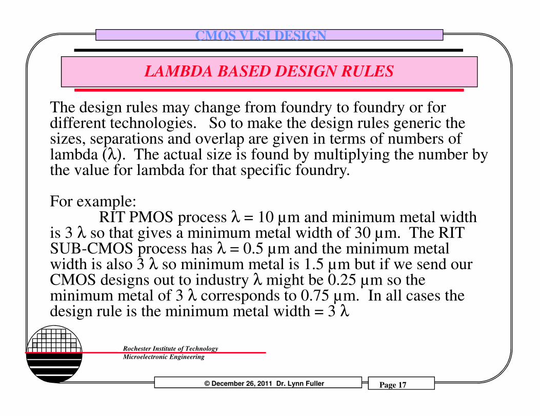
The design rules may change from foundry to foundry or for different technologies. So to make the design rules generic the sizes, separations and overlap are given in terms of numbers of lambda (λ). The actual size is found by multiplying the number by the value for lambda for that specific foundry.
For example:RIT PMOS process λ = 10 µm and minimum metal width
© December 26, 2011 Dr. Lynn Fuller
Rochester Institute of Technology
Microelectronic Engineering
Page 17
For example:RIT PMOS process λ = 10 µm and minimum metal width
is 3 λ so that gives a minimum metal width of 30 µm. The RIT SUB-CMOS process has λ = 0.5 µm and the minimum metal width is also 3 λ so minimum metal is 1.5 µm but if we send our CMOS designs out to industry λ might be 0.25 µm so the minimum metal of 3 λ corresponds to 0.75 µm. In all cases the design rule is the minimum metal width = 3 λ
Page 18
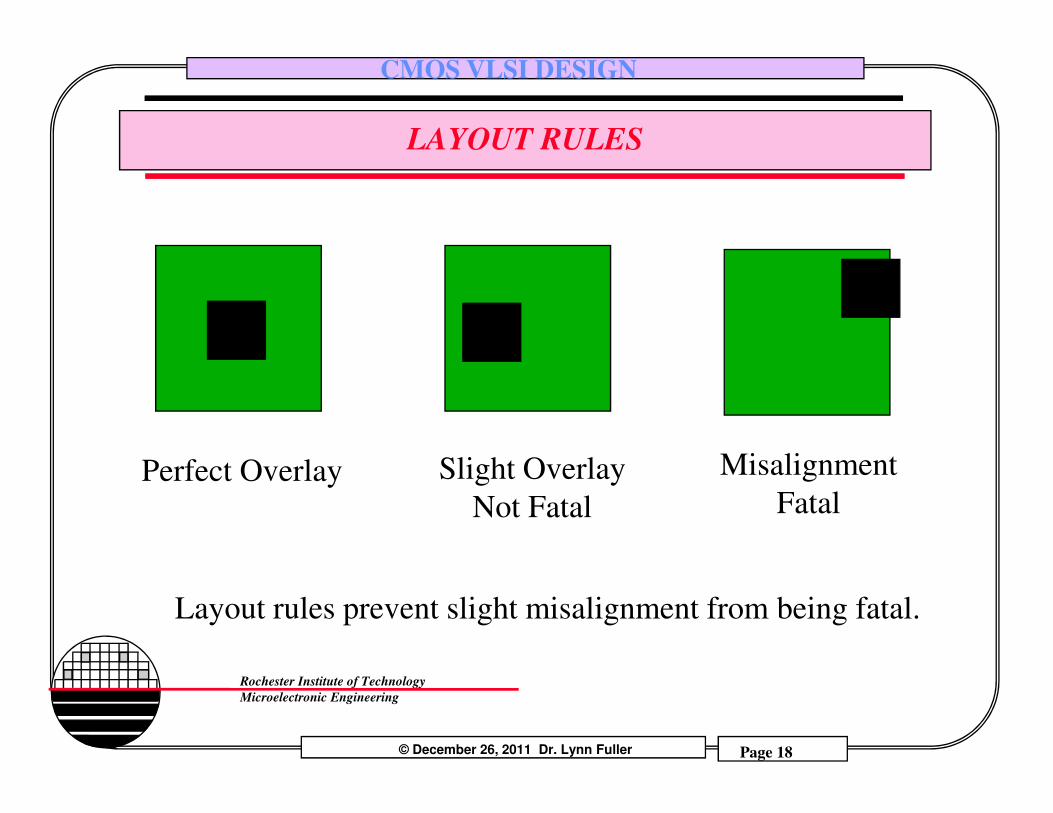
CMOS VLSI DESIGN
LAYOUT RULES
© December 26, 2011 Dr. Lynn Fuller
Rochester Institute of Technology
Microelectronic Engineering
Page 18
Perfect Overlay Slight OverlayNot Fatal
MisalignmentFatal
Layout rules prevent slight misalignment from being fatal.
Page 19
CMOS VLSI DESIGN
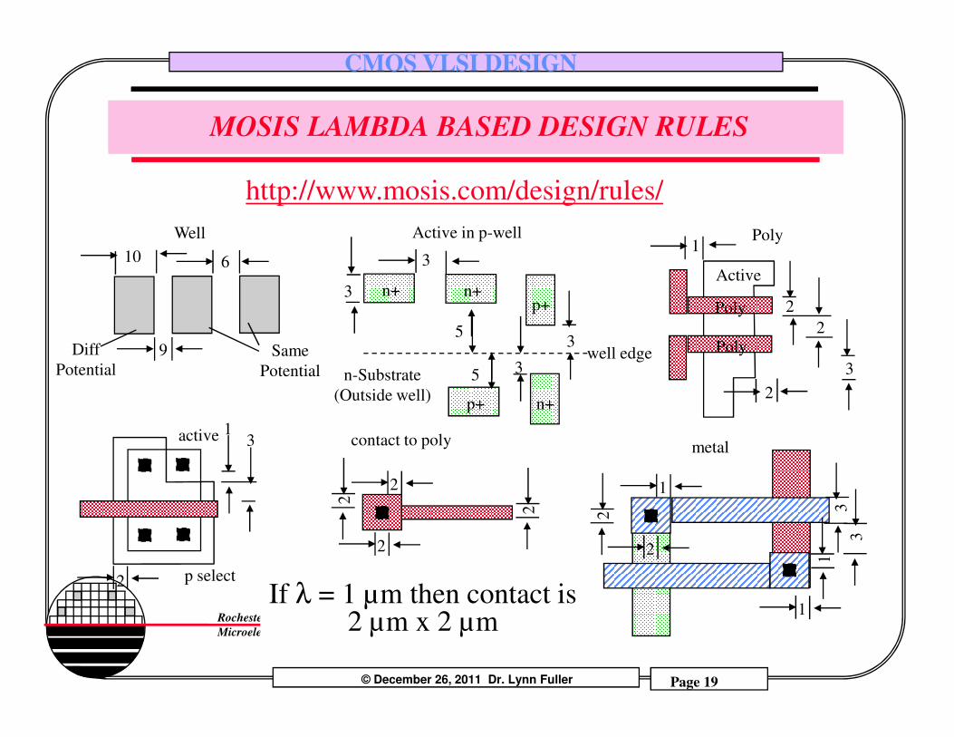
MOSIS LAMBDA BASED DESIGN RULES
10 6
9
Well
SamePotential
DiffPotential
3
3
3
Active in p-well
n+p+
n+
well edgen-Substrate
5
Poly
2
3
2
1
Poly
Poly
Active
5 3
http://www.mosis.com/design/rules/
© December 26, 2011 Dr. Lynn Fuller
Rochester Institute of Technology
Microelectronic Engineering
Page 19
PotentialPotential n-Substrate(Outside well) 2
3
1
p select
active
2
3 contact to poly
2
2
2
2
metal
2
1
2
33
1
1
If λ = 1 µm then contact is2 µm x 2 µm
p+
5
n+
3
Page 20
CMOS VLSI DESIGN
MOSIS LAMBDA BASED DESIGN RULES
metal two2
1
2
43
http://www.mosis.com/design/rules/
MOSIS Educational Program
© December 26, 2011 Dr. Lynn Fuller
Rochester Institute of Technology
Microelectronic Engineering
Page 20
4
1
1 Instructional Processes Include: AMI λ = 0.8 µm SCMOS RulesAMI λ = 0.35 µm SCMOS Rules
Research Processes:go down to poly length of 65nm
Page 21
CMOS VLSI DESIGN
MOSIS REQUIREMENTS
MOSIS requires that projects have successfully passed LVS (Layout Versus Schematic) and DRC (Design Rule Checking). Our MENTOR tools for LVS and DRC (as they are set up) require separate N-select and P-select levels in order to know an NMOS transistor from a PMOS transistor. Although either an N-well, P-well or both will work for a twin well process, we have set up our DRC to look for N-well.
© December 26, 2011 Dr. Lynn Fuller
Rochester Institute of Technology
Microelectronic Engineering
Page 21
look for N-well.
Page 22
CMOS VLSI DESIGN
RIT PROCESSES
At RIT we use the Sub-CMOS and ADV-CMOS processes for most designs. In these processes the minimum poly length is 1µm and 0.5µm respectively. We use scalable MOSIS design rules with lambda equal to 0.5µm and 0.25µm. These processes use one layer of poly and two layers of metal.
The examples on the following pages are designs that could be made
© December 26, 2011 Dr. Lynn Fuller
Rochester Institute of Technology
Microelectronic Engineering
Page 22
The examples on the following pages are designs that could be made with either of the above processes. As a result the designs are generous, meaning that larger than minimum dimensions are used. For example λ = 0.5µm and minimum poly is 2λ but designed at 2.5µm because our poly etch is isotropic.
The design approach for digital circuits is to design primitive cells and then use the primitive cells to design basic cells which are then used in the project designs. A layout approach is also used that allows for easy assembly of these cells into more complex cells.
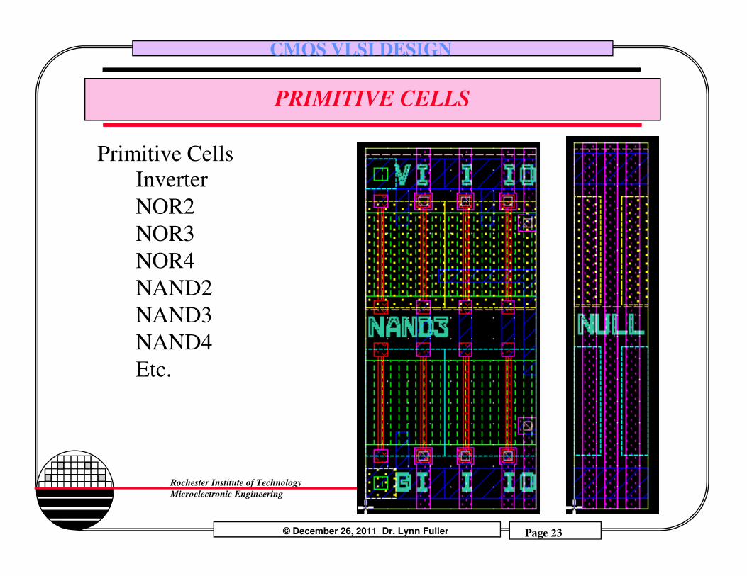
Page 23
CMOS VLSI DESIGN
PRIMITIVE CELLS
InverterNOR2NOR3NOR4NAND2
Primitive Cells
© December 26, 2011 Dr. Lynn Fuller
Rochester Institute of Technology
Microelectronic Engineering
Page 23
NAND2NAND3NAND4Etc.
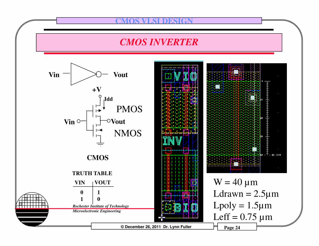
Page 24
CMOS VLSI DESIGN
CMOS INVERTER
Vin Vout
Vin
+V
Vout
Idd
PMOS
© December 26, 2011 Dr. Lynn Fuller
Rochester Institute of Technology
Microelectronic Engineering
Page 24
Vin
CMOS
Vout
TRUTH TABLE
VOUTVIN
0 1
1 0
NMOS
W = 40 µmLdrawn = 2.5µmLpoly = 1.5µmLeff = 0.75 µm
Page 25
CMOS VLSI DESIGN
NOR and NAND
VOUTVB
0 0 1
0 1 0
1 0 0
VA
VAVOUT
VB
+V
VOUTVB
0 0 1
0 1 1
1 0 1
VA
VAVOUT
VB
+V
© December 26, 2011 Dr. Lynn Fuller
Rochester Institute of Technology
Microelectronic Engineering
Page 25
1 0 0
1 1 0
VOUT
VA VB
1 0 1
1 1 0
+V
VOUTVA
VB
Page 26
CMOS VLSI DESIGN
OTHER LOGIC GATES
VAVOUT
VB
VOUTVB
0 0 0 0
VAVOUTVOUTVB
0 0 0
VA VB
0 0 0
VA
VB
VA
VOUT
ORAND 3 INPUT OR3 INPUT AND
VC VOUTVBVA
0 0 0 0
VC
VAVA
VB VB
VC VCVOUT VOUT
© December 26, 2011 Dr. Lynn Fuller
Rochester Institute of Technology
Microelectronic Engineering
Page 26
0 0 1 0
0 1 0 0
0 1 1 0
1 0 0 0
1 0 1 0
1 1 0 0
1 1 1 1
0 1 0
1 0 0
1 1 1
0 0 0
0 1 1
1 0 1
1 1 1
0 0 0 0
0 0 1 1
0 1 0 1
0 1 1 1
1 0 0 1
1 0 1 1
1 1 0 1
1 1 1 1
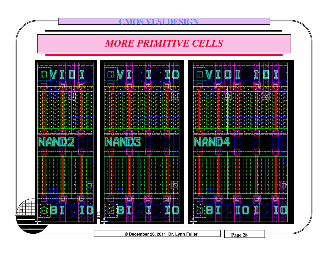
Page 27
CMOS VLSI DESIGN
MORE PRIMITIVE CELLS
© December 26, 2011 Dr. Lynn Fuller
Rochester Institute of Technology
Microelectronic Engineering
Page 27
Page 28
CMOS VLSI DESIGN
MORE PRIMITIVE CELLS
© December 26, 2011 Dr. Lynn Fuller
Rochester Institute of Technology
Microelectronic Engineering
Page 28
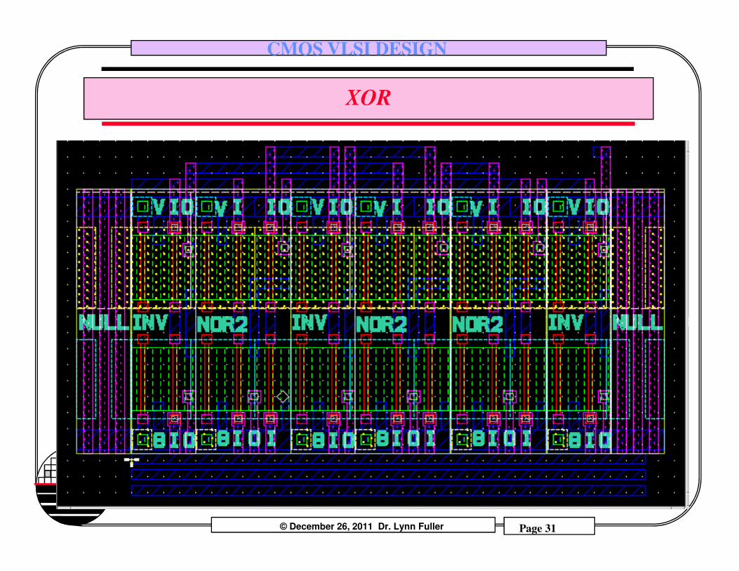
Page 29
CMOS VLSI DESIGN
BASIC CELLS
XORD FFJK FFData Latch
Basic Cells
XOR
A
© December 26, 2011 Dr. Lynn Fuller
Rochester Institute of Technology
Microelectronic Engineering
Page 29
B
Page 30
CMOS VLSI DESIGN
XOR
© December 26, 2011 Dr. Lynn Fuller
Rochester Institute of Technology
Microelectronic Engineering
Page 30
Page 31
CMOS VLSI DESIGN
XOR
© December 26, 2011 Dr. Lynn Fuller
Rochester Institute of Technology
Microelectronic Engineering
Page 31
Page 32
CMOS VLSI DESIGN
FILP-FLOPS
RS FLIP FLOP
QBARS
R QQS
0 0 Qn-1
0 1 1
1 0 0
1 1 INDETERMINATE
R
© December 26, 2011 Dr. Lynn Fuller
Rochester Institute of Technology
Microelectronic Engineering
Page 32
D FLIP FLOP
Q
QBARDATA
Q=DATA IF CLOCK IS HIGH
IF CLOCK IS LOW Q=PREVIOUS DATA VALUE
CLOCK
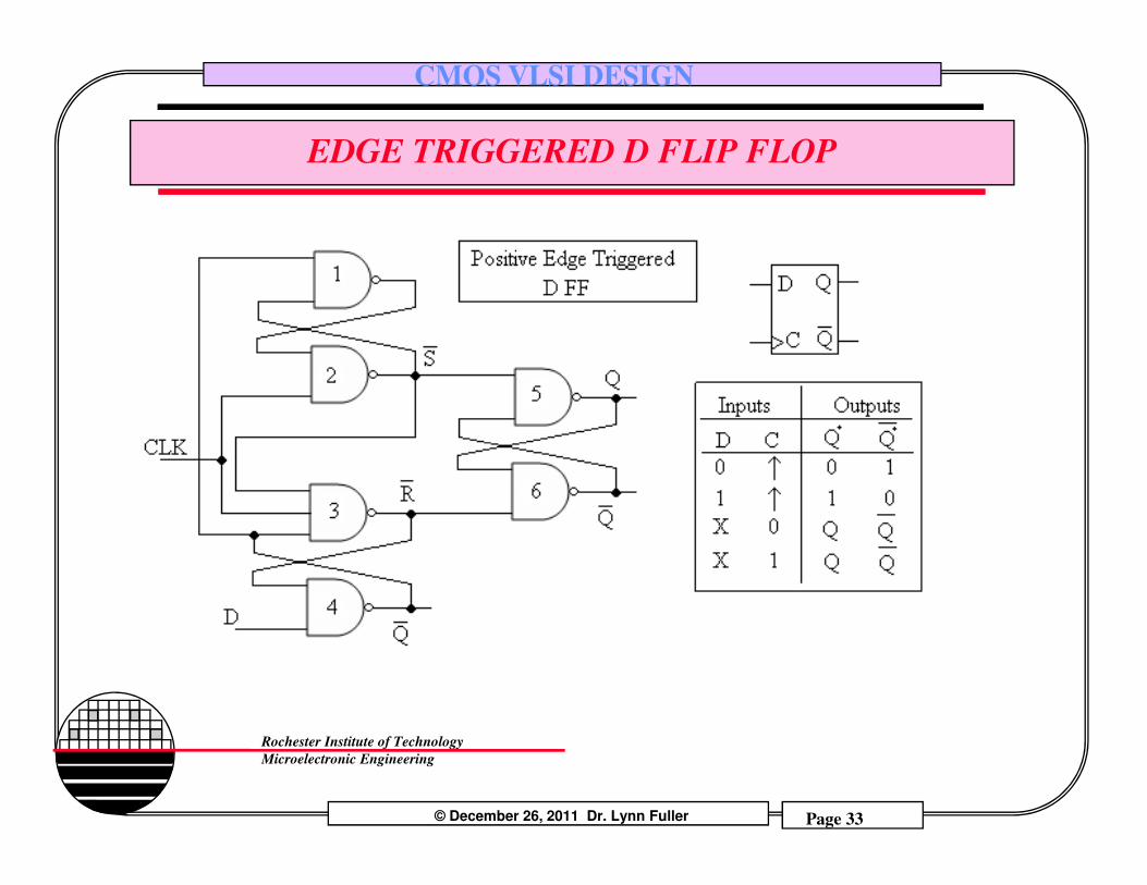
Page 33
CMOS VLSI DESIGN
EDGE TRIGGERED D FLIP FLOP
© December 26, 2011 Dr. Lynn Fuller
Rochester Institute of Technology
Microelectronic Engineering
Page 33
Page 34
CMOS VLSI DESIGN
EDGE TRIGGERED D FLIP FLOP
© December 26, 2011 Dr. Lynn Fuller
Rochester Institute of Technology
Microelectronic Engineering
Page 34
Page 35
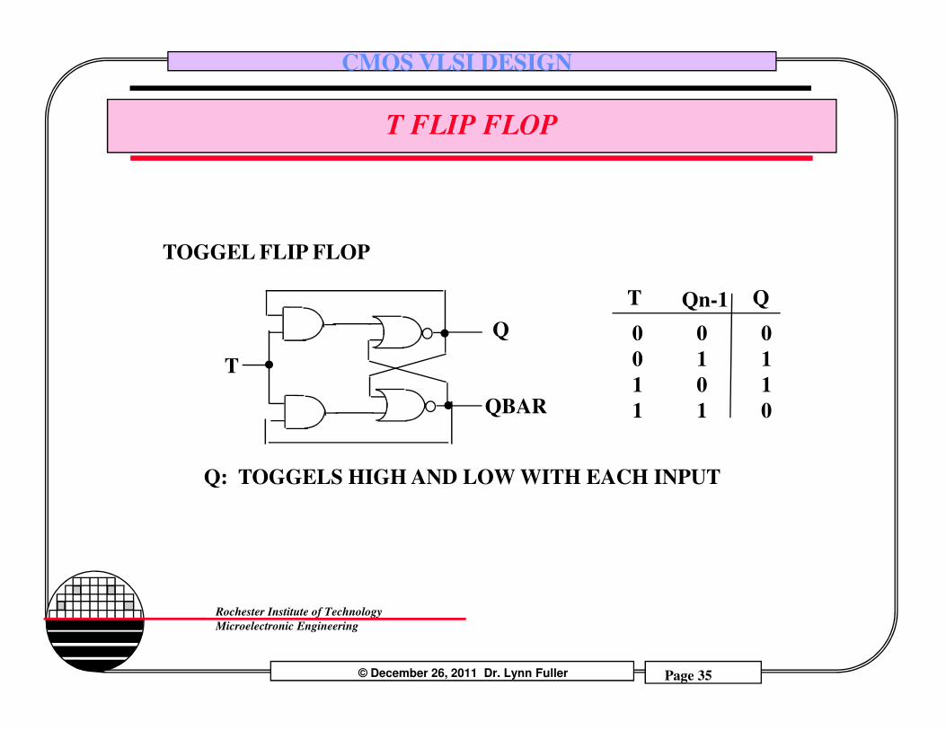
CMOS VLSI DESIGN
T FLIP FLOP
TOGGEL FLIP FLOP
Q
QQn-1
0 0 0
0 1 1
T
T
© December 26, 2011 Dr. Lynn Fuller
Rochester Institute of Technology
Microelectronic Engineering
Page 35
QBAR
Q: TOGGELS HIGH AND LOW WITH EACH INPUT
0 1 1
1 0 1
1 1 0
T
Page 36
CMOS VLSI DESIGN
JK FLIP FLOP
© December 26, 2011 Dr. Lynn Fuller
Rochester Institute of Technology
Microelectronic Engineering
Page 36
Page 37
CMOS VLSI DESIGN
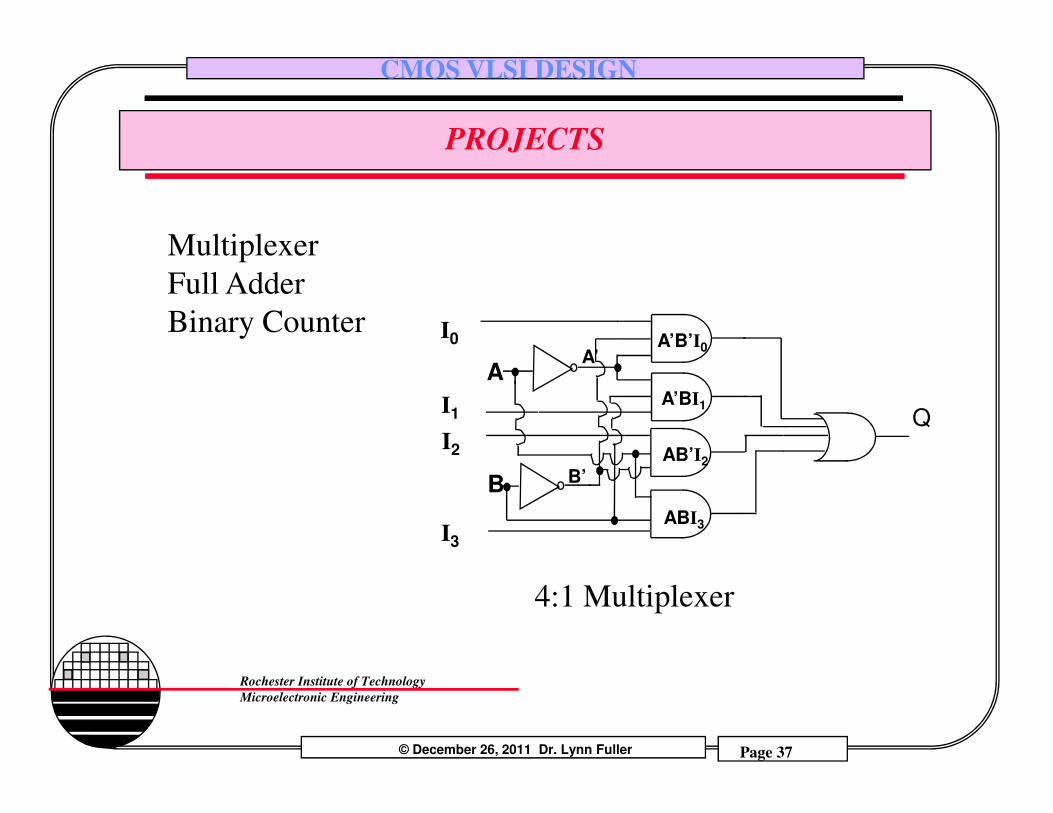
PROJECTS
MultiplexerFull AdderBinary Counter I0
I1 Q
AA’
A’B’I0
A’BI1
© December 26, 2011 Dr. Lynn Fuller
Rochester Institute of Technology
Microelectronic Engineering
Page 37
I1
I2
I3
Q
B B’
A’BI1
AB’I2
ABI3
4:1 Multiplexer
Page 38
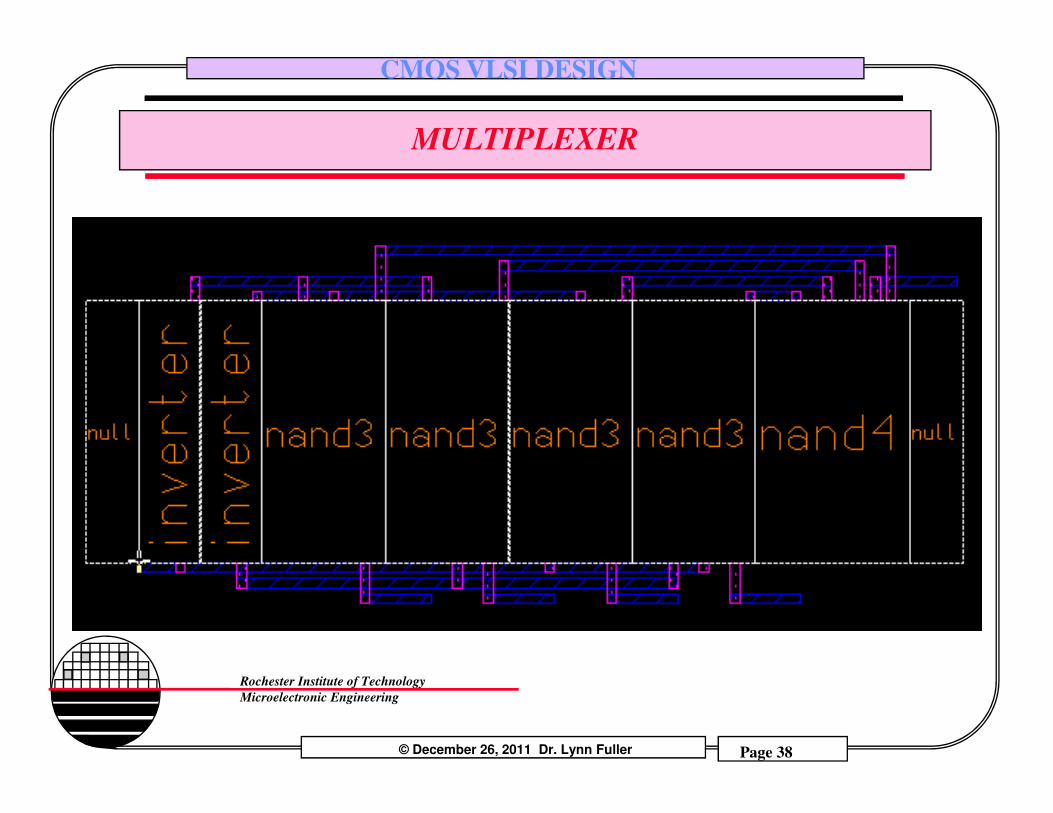
CMOS VLSI DESIGN
MULTIPLEXER
© December 26, 2011 Dr. Lynn Fuller
Rochester Institute of Technology
Microelectronic Engineering
Page 38
Page 39
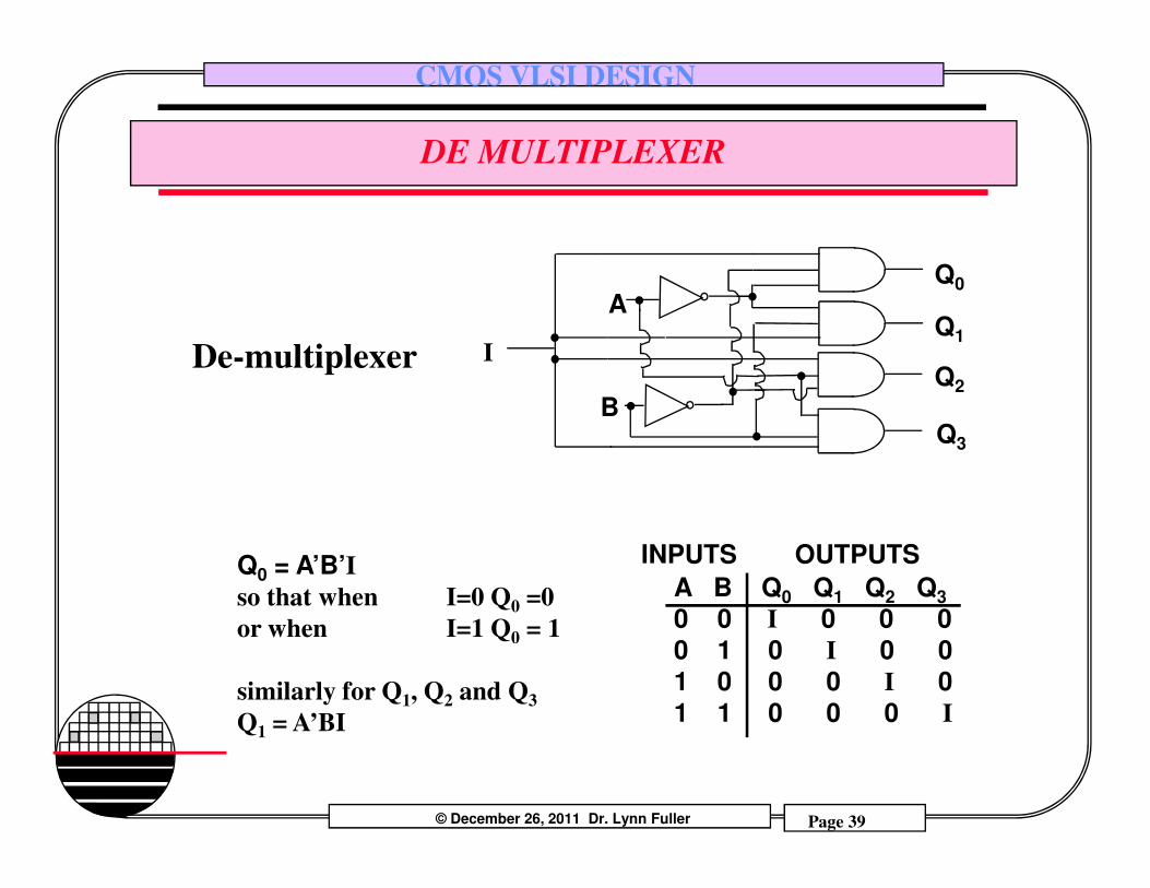
CMOS VLSI DESIGN
DE MULTIPLEXER
De-multiplexer
A
B
I
Q0
Q1
Q2
Q3
© December 26, 2011 Dr. Lynn Fuller
Rochester Institute of Technology
Microelectronic Engineering
Page 39
A B Q0 Q1 Q2 Q3
0 0 I 0 0 00 1 0 I 0 01 0 0 0 I 01 1 0 0 0 I
Q0 = A’B’I
so that when I=0 Q0 =0
or when I=1 Q0 = 1
similarly for Q1, Q2 and Q3
Q1 = A’BI
INPUTS OUTPUTS
Q3
Page 40
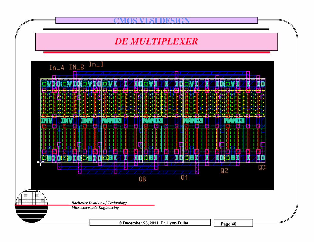
CMOS VLSI DESIGN
DE MULTIPLEXER
© December 26, 2011 Dr. Lynn Fuller
Rochester Institute of Technology
Microelectronic Engineering
Page 40
Page 41
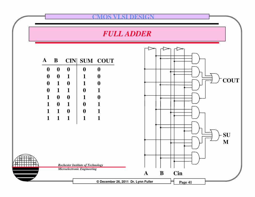
CMOS VLSI DESIGN
FULL ADDER
COUT
SUM COUTBA
0 0 0 0 0
0 0 1 1 0
0 1 0 1 0
0 1 1 0 1
1 0 0 1 0
CIN
© December 26, 2011 Dr. Lynn Fuller
Rochester Institute of Technology
Microelectronic Engineering
Page 41
A CinB
SU
M
1 0 0 1 0
1 0 1 0 1
1 1 0 0 1
1 1 1 1 1
Page 42
CMOS VLSI DESIGN
FULL ADDER
© December 26, 2011 Dr. Lynn Fuller
Rochester Institute of Technology
Microelectronic Engineering
Page 42
Page 43
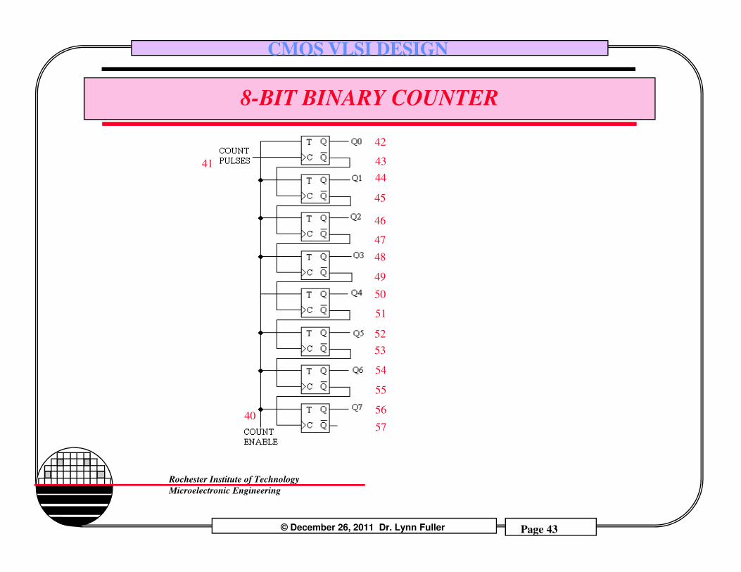
CMOS VLSI DESIGN
8-BIT BINARY COUNTER
42
43
44
45
46
47
48
49
41
© December 26, 2011 Dr. Lynn Fuller
Rochester Institute of Technology
Microelectronic Engineering
Page 43
50
51
52
53
54
55
56
5740
Page 44
CMOS VLSI DESIGN
8-BIT BINARY COUNTER
© December 26, 2011 Dr. Lynn Fuller
Rochester Institute of Technology
Microelectronic Engineering
Page 44
Page 45
CMOS VLSI DESIGN
FILE FORMATS
Mentor- ICGraph files (filename.iccel), all layers, polygons with up to 200 vertices
GDS2- CALMA files (old IC design tool) (filename.gds), all layers, polygons
© December 26, 2011 Dr. Lynn Fuller
Rochester Institute of Technology
Microelectronic Engineering
Page 45
layers, polygons
MEBES- files for electron beam maskmaking tool, each file one layer, trapezoids only
Page 46
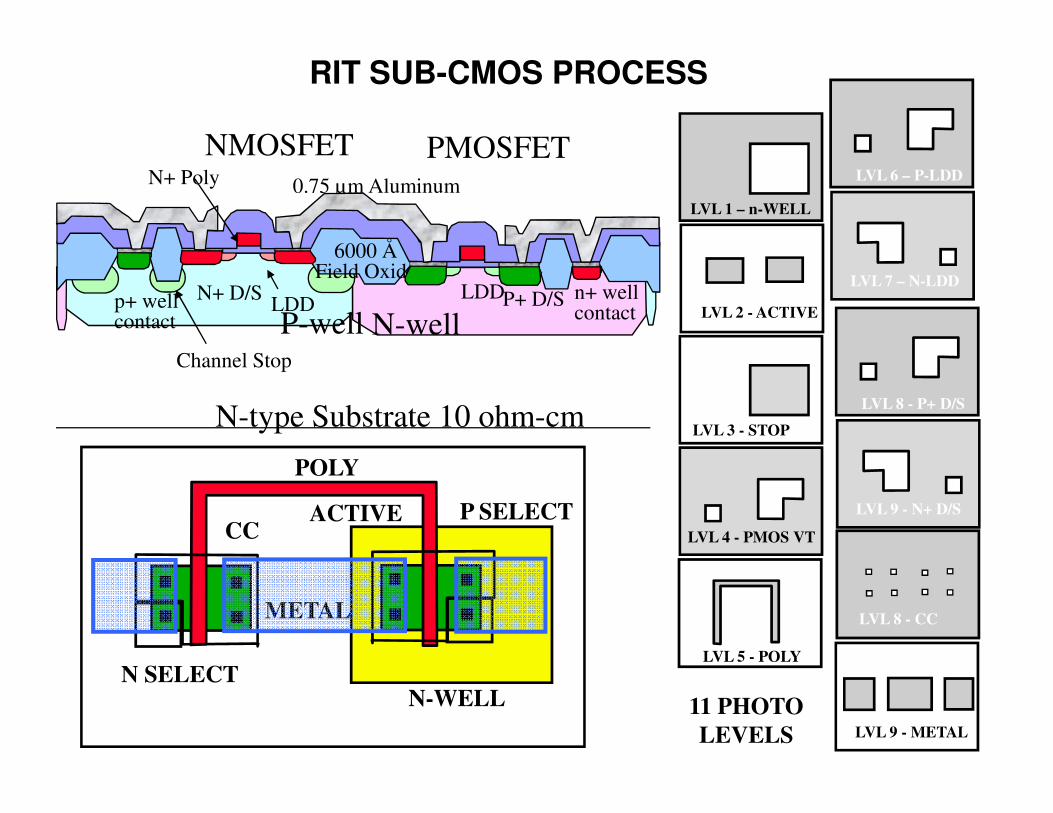
RIT SUB-CMOS PROCESS
0.75 µm Aluminum
N-type Substrate 10 ohm-cm
P-well N-well
6000 ÅField Oxide
NMOSFET PMOSFETN+ Poly
Channel Stop
P+ D/SN+ D/S LDDLDD n+ well
contactp+ wellcontact
LVL 1 – n-WELL
LVL 2 - ACTIVE
LVL 8 - P+ D/S
LVL 7 – N-LDD
LVL 6 – P-LDD
11 PHOTO
LEVELS
POLY
METAL
N-WELL
P SELECTCC
ACTIVE
N-type Substrate 10 ohm-cm
LVL 9 - METAL
LVL 4 - PMOS VT
LVL 9 - N+ D/S
LVL 8 - P+ D/S
LVL 3 - STOP
LVL 8 - CC
LVL 5 - POLY
N SELECT
Page 47
RIT ADVANCED CMOS
LVL 2 - NWell
LVL 3 - Pwell
LVL 8 - NLDD
LVL 9 – N+D/S
LVL 7 - PLDDNMOSFET PMOSFET
N-wellP-well
N+ Poly
P+ D/SN+ D/S
LDDLDD
n+ wellcontact
p+ wellcontact
P+ PolyLVL 1 - STI
12 PHOTO LEVELS + 2 FOR EACH ADDITIONAL
METAL LAYER
POLY
METAL
N-WELL
P SELECTCC
ACTIVE
N SELECT
LVL 6 - POLY
LVL 11 - CC
LVL 12 – METAL 1
LVL 10 – P+D/SLVL 4 - VTP
METAL LAYER
LVL 5 - VTN
Page 48
CMOS VLSI DESIGN
OTHER MASKMAKING FEATURES
Fiducial Marks-marks on the edge of the mask used to align the mask to the stepper
BarcodesTitlesAlignment Keys- marks on the die from a previous
© December 26, 2011 Dr. Lynn Fuller
Rochester Institute of Technology
Microelectronic Engineering
Page 48
Alignment Keys- marks on the die from a previous level used to align the wafer to the stepper
CD Resolution Targets- lines and spacesOverlay Verniers- structures that allow measurement
of x and y overlay accuracyTilingOptical Proximity Correction (OPC)
Page 49
CMOS VLSI DESIGN
REFERENCES
1. Silicon Processing for the VLSI Era, Volume 1 – Process Technology, 2nd, S. Wolf and R.N. Tauber, Lattice Press.
2. The Science and Engineering of Microelectronic Fabrication, Stephen A. Campbell, Oxford University Press, 1996.
3. MOSIS Scalable CMOS Design Rules for Generic CMOS Processes, www.mosis.org, and
© December 26, 2011 Dr. Lynn Fuller
Rochester Institute of Technology
Microelectronic Engineering
Page 49
Processes, www.mosis.org, and http://www.mosis.com/design/rules/
Page 50
CMOS VLSI DESIGN
HOMEWORK - CMOS VLSI DESIGN
1. Sketch and label the seven layout layers of a CMOS 2-input OR gate that uses the MOSIS lambda based design rules and uses minimum area. Calculate the area of the smallest rectangle to enclose the design in µm2 .
2. What lithographic layers are not drawn by the designer in the Adv-CMOS process? How are they created?
© December 26, 2011 Dr. Lynn Fuller
Rochester Institute of Technology
Microelectronic Engineering
Page 50
Adv-CMOS process? How are they created?3. For the SUB-CMOS layout shown below sketch the crossection
A-A’ just after level 5 lithography. 4. Does the designer put the
alignment marks, fiducial marks, barcode, resolution and overlay features on the design?
A’
A