CMOS devices and manufacturing technology. CMOS logic gates and their layout. Propagation delay, noise margins, and power dissipation. Combinational (e.g., arithmetic) and sequential circuit design. Memory circuit design.
Course goals
Ability to design and implement CMOS digital circuits and optimize them with respect to different constraints: size (cost), speed, power dissipation, and reliability
What is the most important invention for the last 50 years?
Sp13 CMPEN 411 L01 S7
The evolution of IC
When was the first transistor invented?
A. 1945 B. 1947 C. 1951 D. 1958
The inventors were in which company?
A. IBM B. Bell Lab C. TI D. Motorola
Sp13 CMPEN 411 L01 S8
The evolution of IC
When was the first transistor invented?
Modern-day electronics began with the invention in 1947 of the transfer resistor, also known as the bi-polar transistor by Bardeen et.al at Bell Laboratories
Sp13 CMPEN 411 L01 S9
The evolution of IC
When was the first IC invented?
A. 1956 B. 1958 C. 1959 D. 1961
The inventor was with which company?
A. IBM B. Bell Labs C. TI D. Motorola
Sp13 CMPEN 411 L01 S10
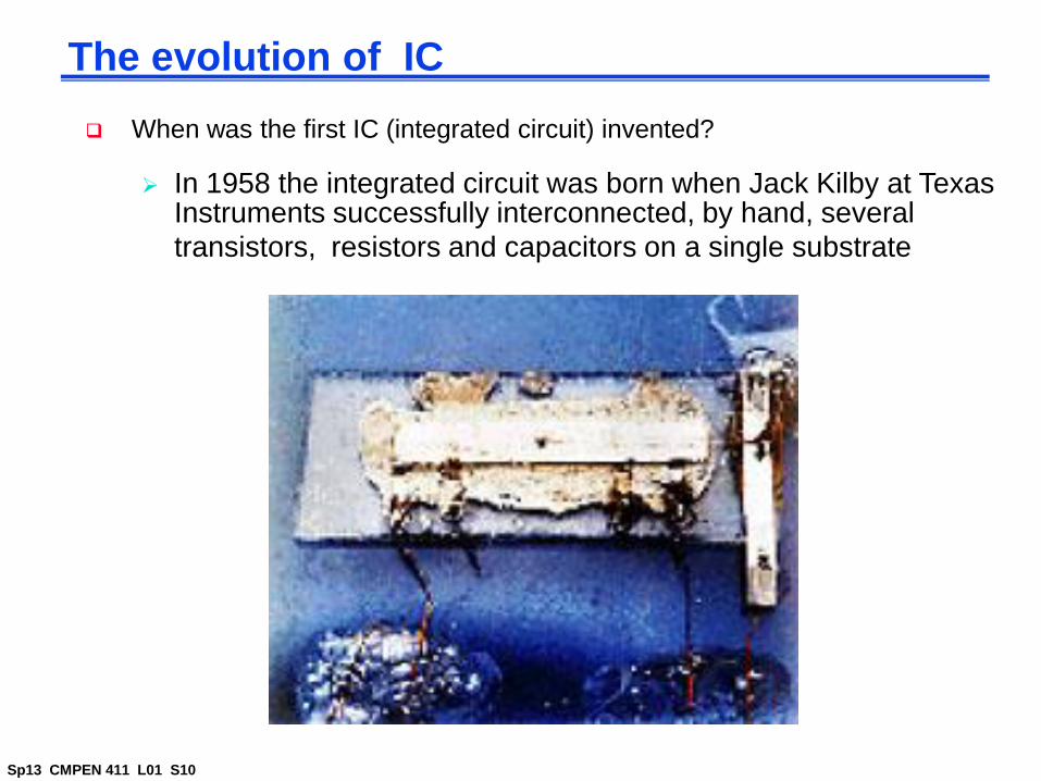
The evolution of IC
When was the first IC (integrated circuit) invented?
In 1958 the integrated circuit was born when Jack Kilby at Texas Instruments successfully interconnected, by hand, several
transistors, resistors and capacitors on a single substrate
Sp13 CMPEN 411 L01 S11
Transistor Revolution
Transistor –Bardeen et.al. (Bell Labs) in 1947
Bipolar transistor – Schockley in 1949
First bipolar digital logic gate – Harris in 1956
First monolithic IC – Jack Kilby in 1958
First commercial IC logic gates – Fairchild 1960
Sp13 CMPEN 411 L01 S12
MOSFET Technology
MOSFET transistor - Lilienfeld (Canada) in 1925 and Heil (England) in 1935
CMOS – 1960‟s, but plagued with manufacturing problems (used in watches due to their power limitations)
PMOS in 1960‟s (calculators)
NMOS in 1970‟s (4004, 8080) – for speed
CMOS in 1980‟s – preferred MOSFET technology because of power benefits
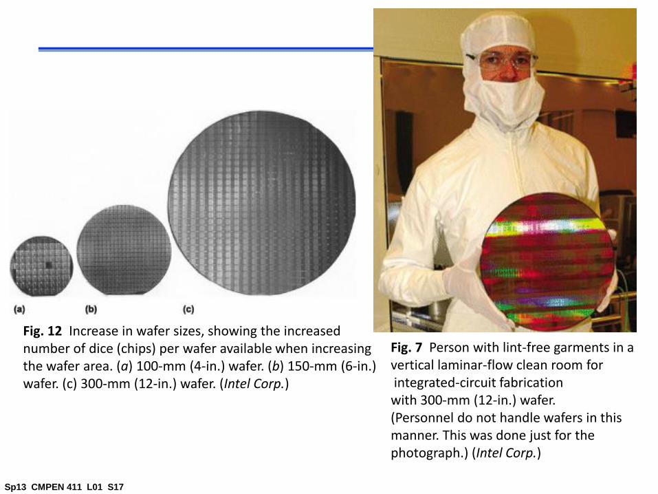
Fig. 12 Increase in wafer sizes, showing the increased number of dice (chips) per wafer available when increasing the wafer area. (a) 100-mm (4-in.) wafer. (b) 150-mm (6-in.) wafer. (c) 300-mm (12-in.) wafer. (Intel Corp.)
Fig. 7 Person with lint-free garments in a vertical laminar-flow clean room forintegrated-circuit fabrication with 300-mm (12-in.) wafer. (Personnel do not handle wafers in this manner. This was done just for the photograph.) (Intel Corp.)
Sp13 CMPEN 411 L01 S18
Sp13 CMPEN 411 L01 S19
Sp13 CMPEN 411 L01 S20
Sp13 CMPEN 411 L01 S21
Sp13 CMPEN 411 L01 S22
Sp13 CMPEN 411 L01 S23
Sp13 CMPEN 411 L01 S24
Sp13 CMPEN 411 L01 S25
Sp13 CMPEN 411 L01 S26
Sp13 CMPEN 411 L01 S27
Sp13 CMPEN 411 L01 S28
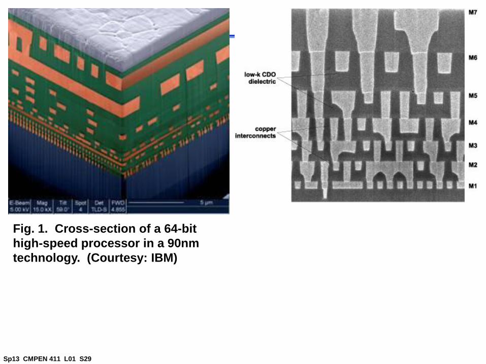
Sp13 CMPEN 411 L01 S29
Fig. 1. Cross-section of a 64-bit
high-speed processor in a 90nm
technology. (Courtesy: IBM)
Sp13 CMPEN 411 L01 S30
Sp13 CMPEN 411 L01 S31
Sp13 CMPEN 411 L01 S32
Sp13 CMPEN 411 L01 S33
Sp13 CMPEN 411 L01 S34
Sp13 CMPEN 411 L01 S35
Sp13 CMPEN 411 L01 S36
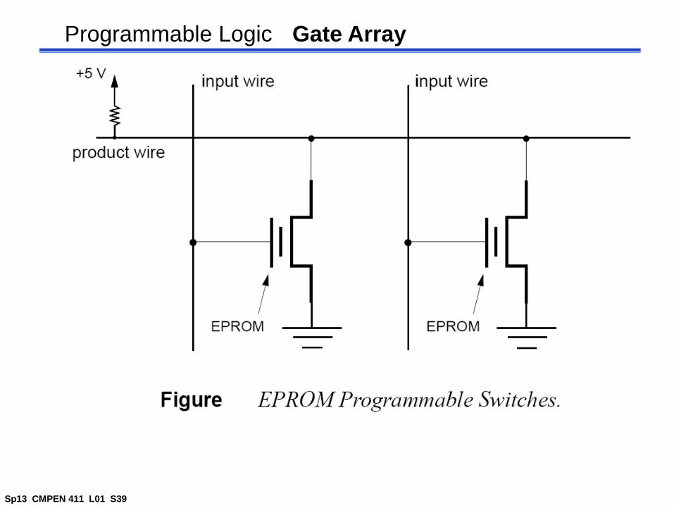
Programmable Logic Gate Array
Sp13 CMPEN 411 L01 S37
Programmable Logic Gate Array
Sp13 CMPEN 411 L01 S38
Programmable Logic Gate Array
Sp13 CMPEN 411 L01 S39
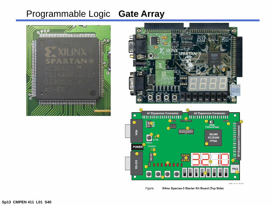
Programmable Logic Gate Array
Sp13 CMPEN 411 L01 S40
Programmable Logic Gate Array
Sp13 CMPEN 411 L01 S41
Programmable Logic Gate Array
Sp13 CMPEN 411 L01 S42
Sp13 CMPEN 411 L01 S43
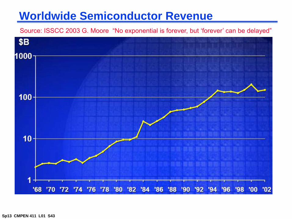
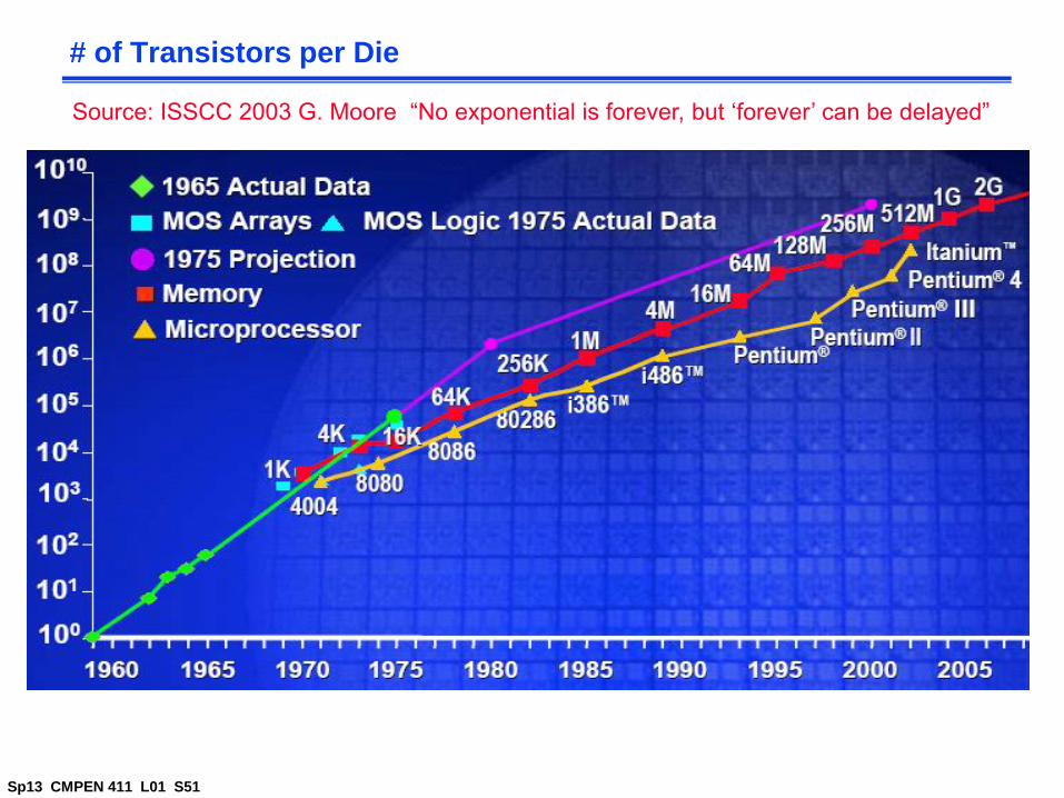
Worldwide Semiconductor RevenueSource: ISSCC 2003 G. Moore “No exponential is forever, but „forever‟ can be delayed”
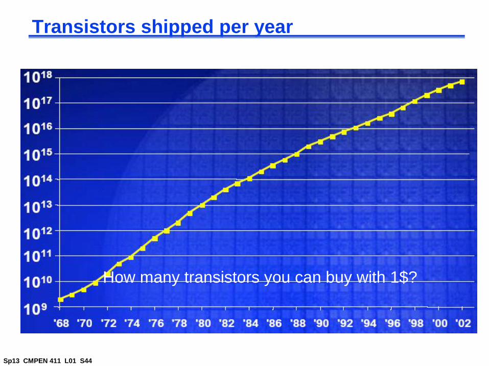
Sp13 CMPEN 411 L01 S44
Transistors shipped per year
How many transistors you can buy with 1$?
Sp13 CMPEN 411 L01 S45
Average Transistor Price by Year
Sp13 CMPEN 411 L01 S46
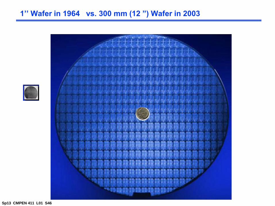
1’’ Wafer in 1964 vs. 300 mm (12 ”) Wafer in 2003
Sp13 CMPEN 411 L01 S47
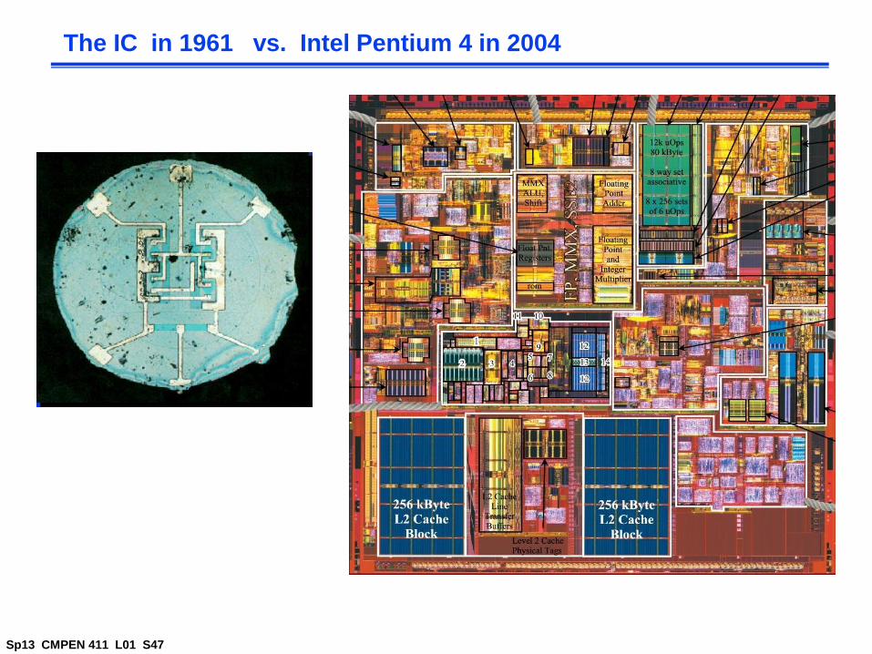
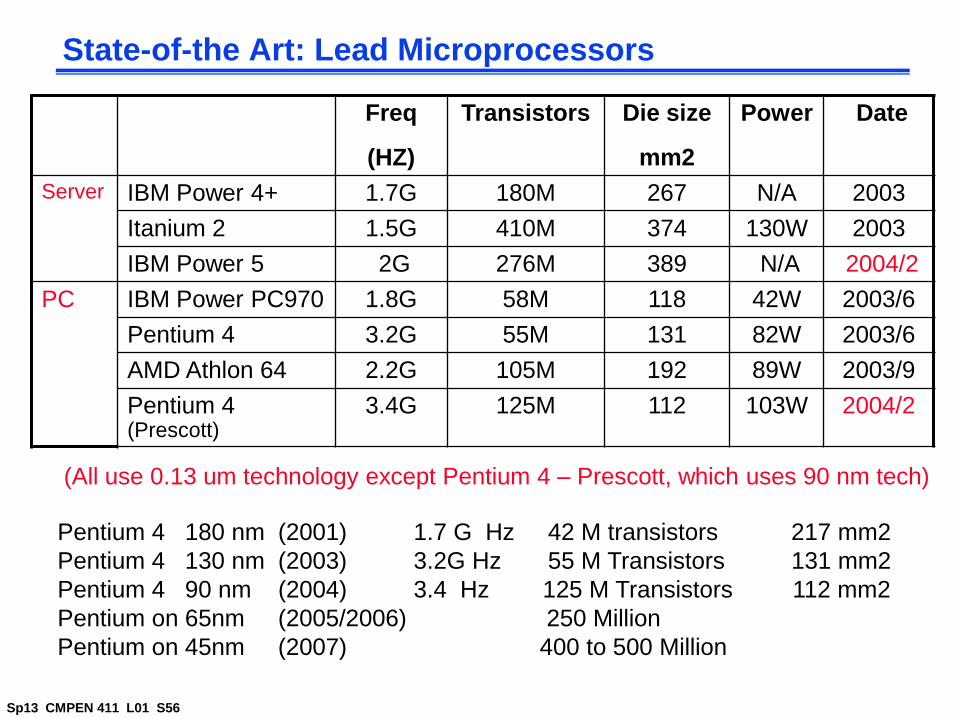
The IC in 1961 vs. Intel Pentium 4 in 2004
Sp13 CMPEN 411 L01 S48
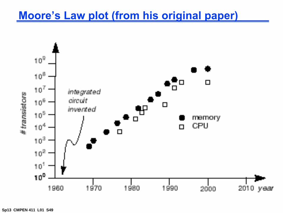
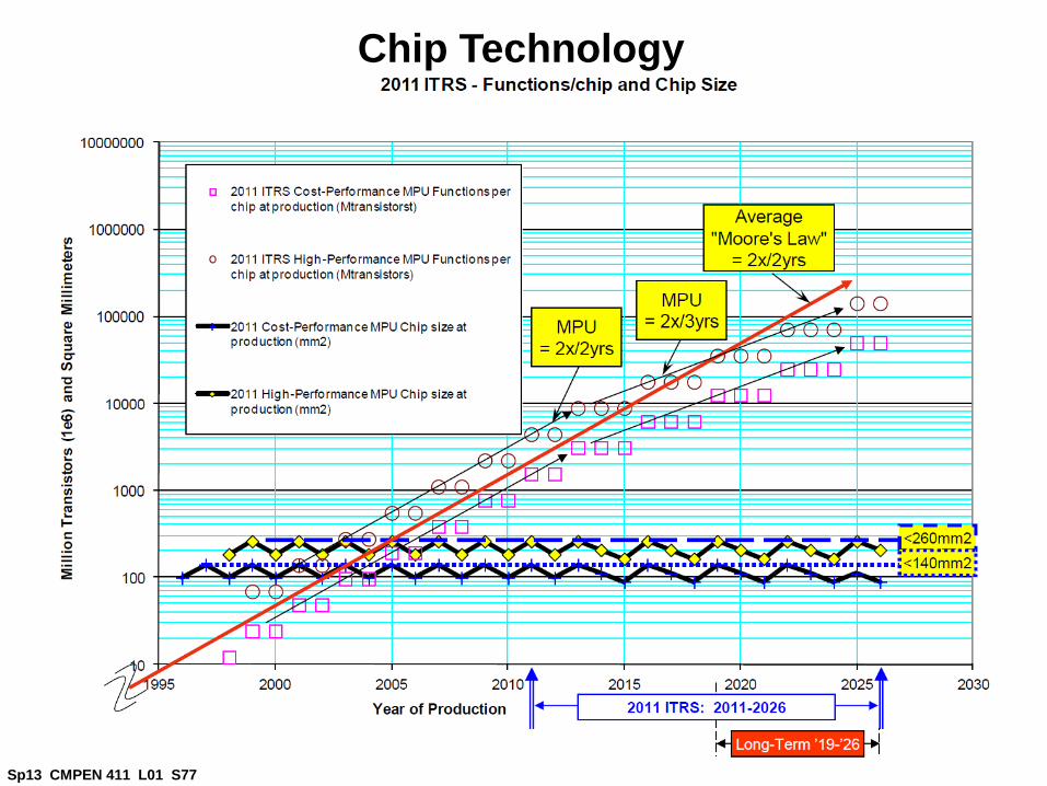
Moore’s Law
In 1965, Gordon Moore predicted that the number of transistors that can be integrated on a die would double every 18 months (i.e., grow exponentially with time).
Amazingly visionary – million transistor/chip barrier was crossed in the 1980‟s.