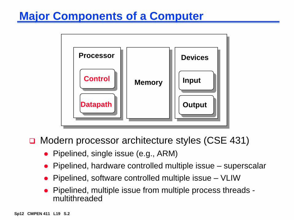
Pipelined, multiple issue from multiple process threads -multithreaded
Sp12 CMPEN 411 L19 S.3
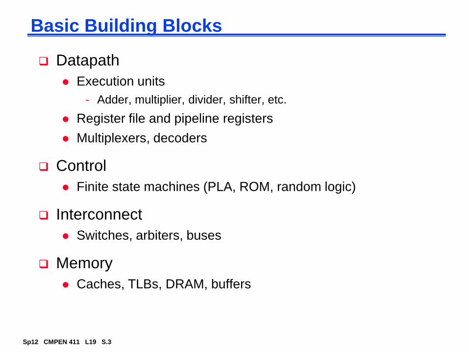
Basic Building Blocks
Datapath
Execution units
- Adder, multiplier, divider, shifter, etc.
Register file and pipeline registers
Multiplexers, decoders
Control
Finite state machines (PLA, ROM, random logic)
Interconnect
Switches, arbiters, buses
Memory
Caches, TLBs, DRAM, buffers
Sp12 CMPEN 411 L19 S.4
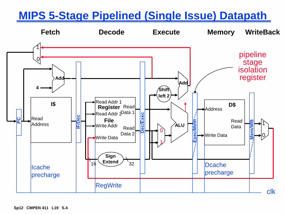
MIPS 5-Stage Pipelined (Single Issue) Datapath
Read
Address
I$
Add
PC
4
0
1
Write Data
Read Addr 1
Read Addr 2
Write Addr
Register
File
Read
Data 1
Read
Data 2
Sign
Extend16 32
ALU
1
0
Shift
left 2
Add
D$Address
Write Data
Read
Data1
0
IF/D
ec
De
c/E
xec
Ex
ec
/Mem
Me
m/W
B
pipelinestage
isolationregister
Fetch Decode Execute Memory WriteBack
clk
Icache
precharge
Dcache
precharge
RegWrite
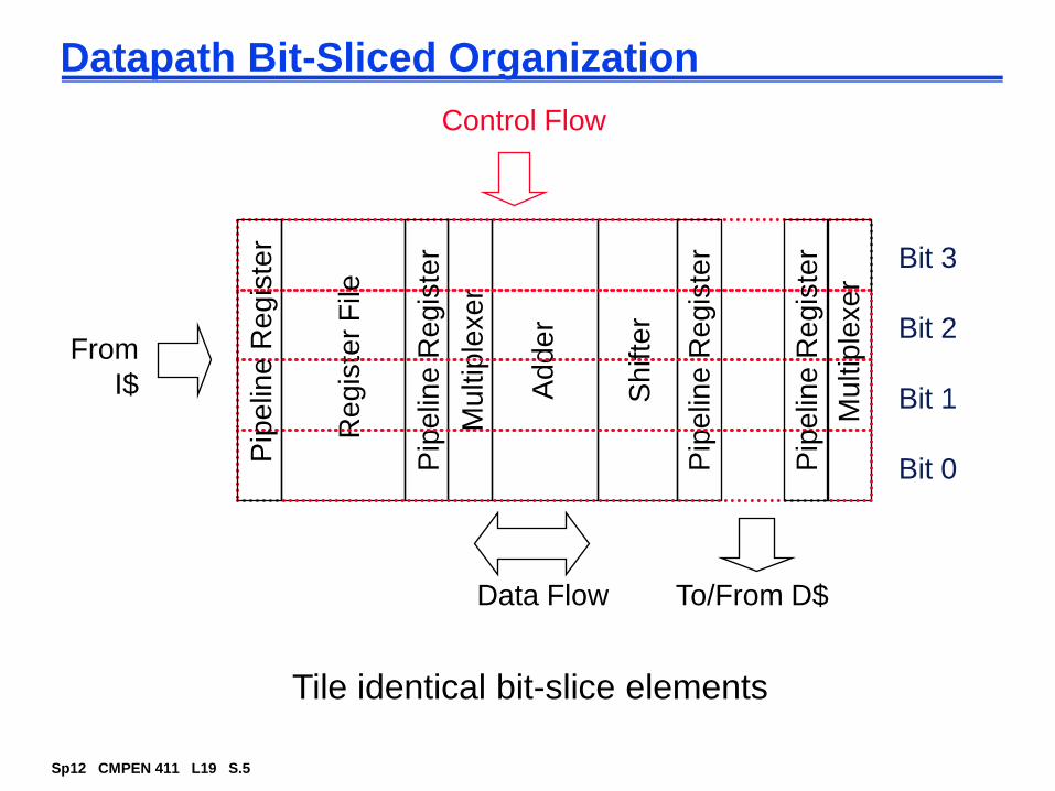
Sp12 CMPEN 411 L19 S.5
Datapath Bit-Sliced Organization
Control Flow
Bit 0
Bit 1
Bit 2
Bit 3
Tile identical bit-slice elements
Re
gis
ter
File
Pip
elin
e R
eg
iste
r
Adder
Sh
ifte
r
Pip
elin
e R
eg
iste
r
Mu
ltip
lexe
r
Mu
ltip
lexe
r
Data Flow
Pip
elin
e R
eg
iste
r
From
I$
Pip
elin
e R
eg
iste
r
To/From D$
Sp12 CMPEN 411 L19 S.6
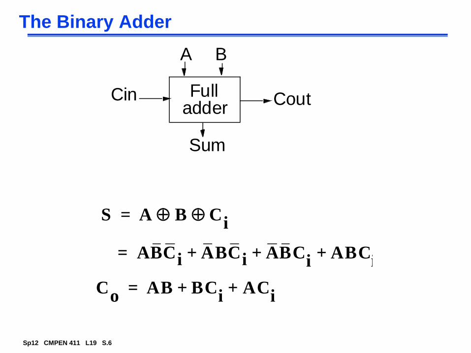
The Binary Adder
S A B Ci
=
A= BCi ABCi ABCi
ABCi
+ + +
Co
AB BCi
ACi
+ +=
A B
Cout
Sum
Cin Fulladder
Sp12 CMPEN 411 L19 S.7
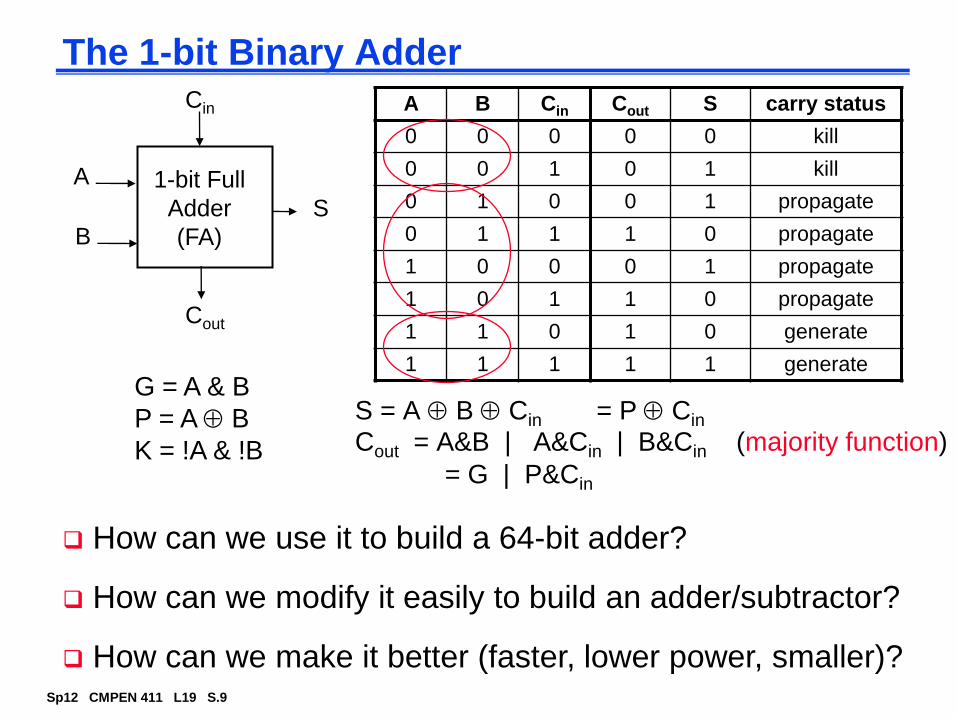
The 1-bit Binary Adder
1-bit Full
Adder
(FA)
A
B
S
Cin
S = A B Cin
Cout = A&B | A&Cin | B&Cin (majority function)
A VERY common operation –often in the critical path
A B Cin Cout S carry status
0 0 0 0 0 kill
0 0 1 0 1 kill
0 1 0 0 1 propagate
0 1 1 1 0 propagate
1 0 0 0 1 propagate
1 0 1 1 0 propagate
1 1 0 1 0 generate
1 1 1 1 1 generate
Cout
G = A & B
P = A B
K = !A & !B
= P Cin
= G | P&Cin
Sp12 CMPEN 411 L19 S.8
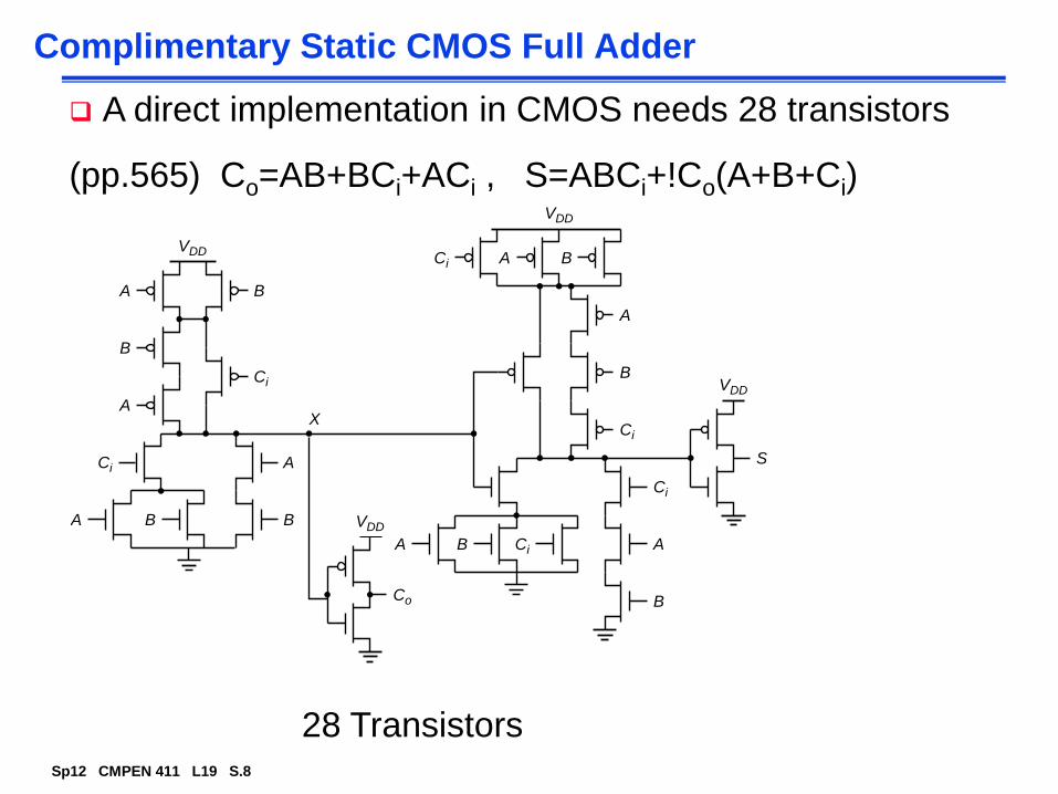
Complimentary Static CMOS Full Adder
28 Transistors
A B
B
A
Ci
Ci A
X
VDD
VDD
A B
Ci BA
B VDD
A
B
Ci
Ci
A
B
A CiB
Co
VDD
S
A direct implementation in CMOS needs 28 transistors
(pp.565) Co=AB+BCi+ACi , S=ABCi+!Co(A+B+Ci)
Sp12 CMPEN 411 L19 S.9
The 1-bit Binary Adder
1-bit Full
Adder
(FA)
A
B
S
Cin
S = A B Cin
Cout = A&B | A&Cin | B&Cin (majority function)
How can we use it to build a 64-bit adder?
How can we modify it easily to build an adder/subtractor?
How can we make it better (faster, lower power, smaller)?
A B Cin Cout S carry status
0 0 0 0 0 kill
0 0 1 0 1 kill
0 1 0 0 1 propagate
0 1 1 1 0 propagate
1 0 0 0 1 propagate
1 0 1 1 0 propagate
1 1 0 1 0 generate
1 1 1 1 1 generate
Cout
G = A & B
P = A B
K = !A & !B
= P Cin
= G | P&Cin
Sp12 CMPEN 411 L19 S.10
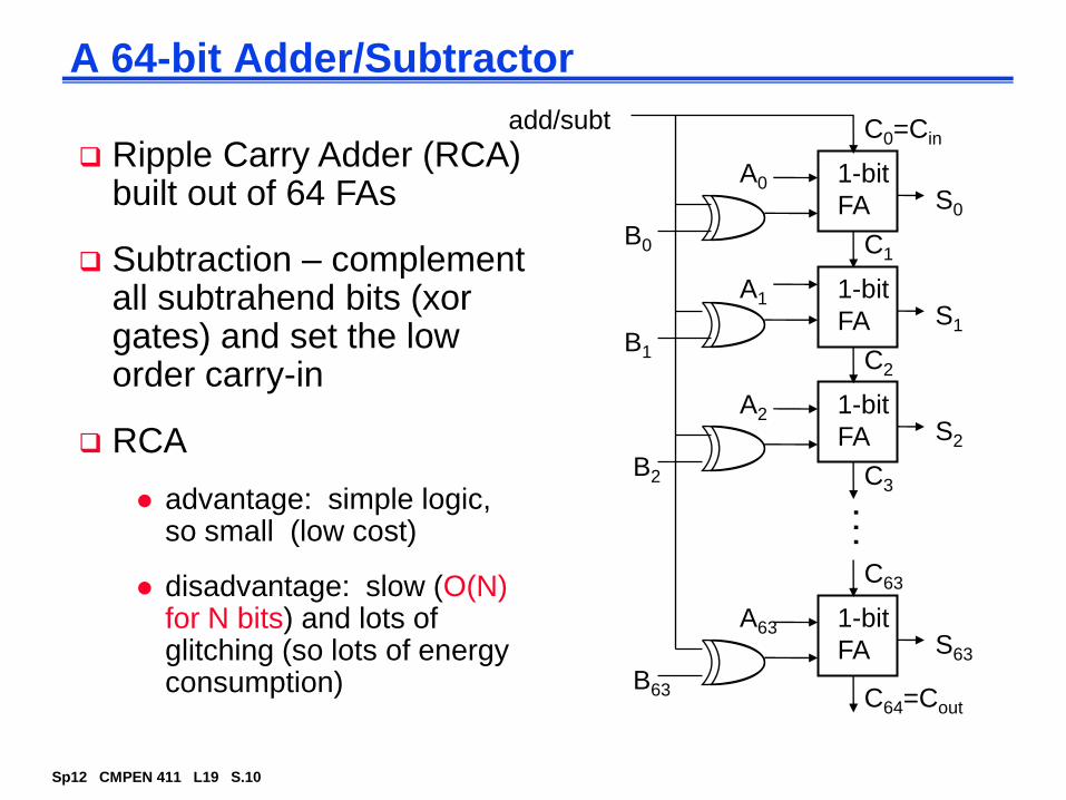
A 64-bit Adder/Subtractor
1-bit
FA S0
C0=Cin
C1
1-bit
FA S1
C2
1-bit
FA S2
C3
C64=Cout
1-bit
FA S63
C63
. .
.
Ripple Carry Adder (RCA) built out of 64 FAs
Subtraction – complement all subtrahend bits (xor gates) and set the low order carry-in
RCA
advantage: simple logic, so small (low cost)
disadvantage: slow (O(N) for N bits) and lots of glitching (so lots of energy consumption)
A0
B0
A1
B1
A2
B2
A63
B63
add/subt
Sp12 CMPEN 411 L19 S.11
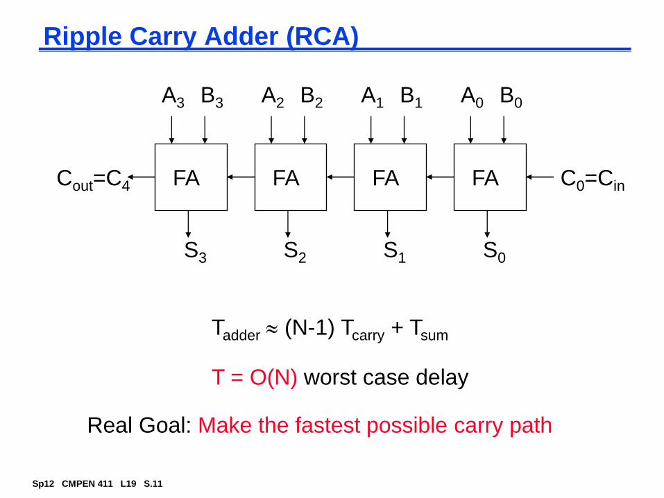
Ripple Carry Adder (RCA)
A0 B0
S0
C0=CinFA
A1 B1
S1
FA
A2 B2
S2
FA
A3 B3
S3
FACout=C4
T = O(N) worst case delay
Tadder (N-1) Tcarry + Tsum
Real Goal: Make the fastest possible carry path
Sp12 CMPEN 411 L19 S.12
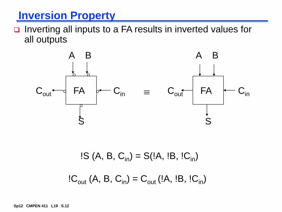
Inversion Property
A B
S
CinFA
!Cout (A, B, Cin) = Cout (!A, !B, !Cin)
Cout
A B
S
FACout Cin
!S (A, B, Cin) = S(!A, !B, !Cin)
Inverting all inputs to a FA results in inverted values for all outputs
Sp12 CMPEN 411 L19 S.13
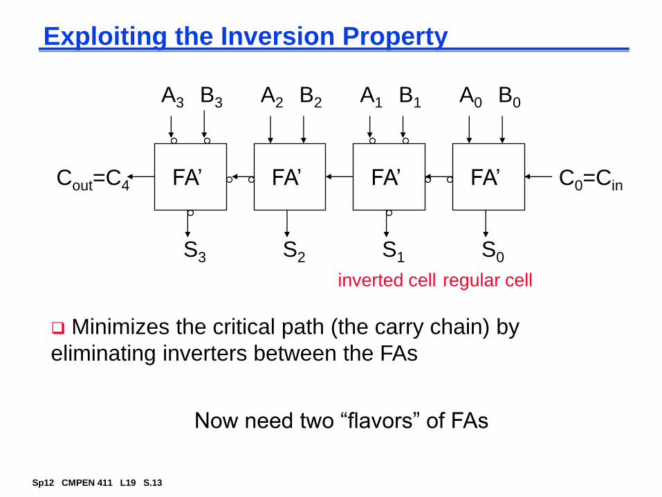
Exploiting the Inversion Property
A0 B0
S0
C0=CinFA’
A1 B1
S1
FA’
A2 B2
S2
FA’
A3 B3
S3
FA’Cout=C4
Now need two “flavors” of FAs
regular cellinverted cell
Minimizes the critical path (the carry chain) by
eliminating inverters between the FAs
Sp12 CMPEN 411 L19 S.14
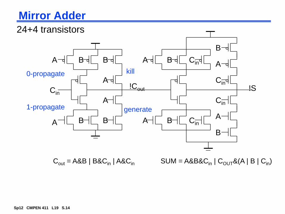
Mirror Adder
B
B B
B B
B
B
B
A
A
A
A
A
AA
A
Cin
Cin
Cin
Cin
Cin!Cout !S
24+4 transistors
kill
generate
0-propagate
1-propagate
Cout = A&B | B&Cin | A&Cin SUM = A&B&Cin | COUT&(A | B | Cin)
Sp12 CMPEN 411 L19 S.15
Mirror Adder Features
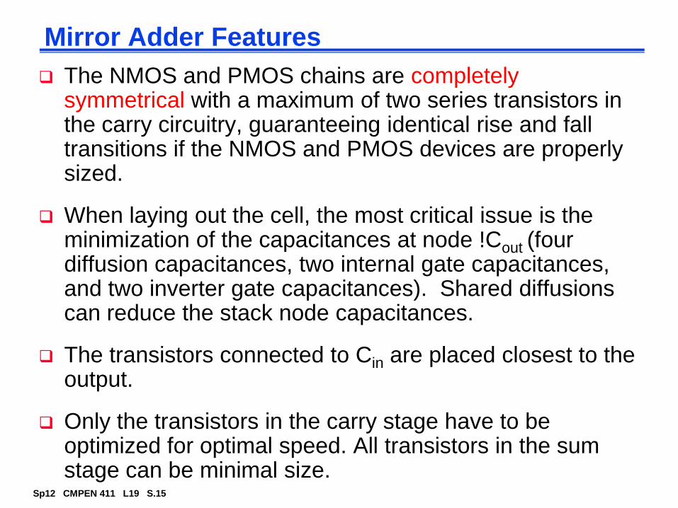
The NMOS and PMOS chains are completely symmetrical with a maximum of two series transistors in the carry circuitry, guaranteeing identical rise and fall transitions if the NMOS and PMOS devices are properly sized.
When laying out the cell, the most critical issue is the minimization of the capacitances at node !Cout (four diffusion capacitances, two internal gate capacitances, and two inverter gate capacitances). Shared diffusions can reduce the stack node capacitances.
The transistors connected to Cin are placed closest to the output.
Only the transistors in the carry stage have to be optimized for optimal speed. All transistors in the sum stage can be minimal size.
Sp12 CMPEN 411 L19 S.16
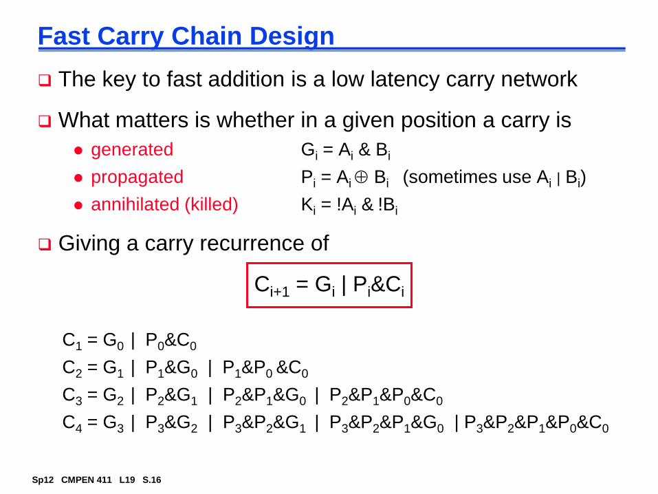
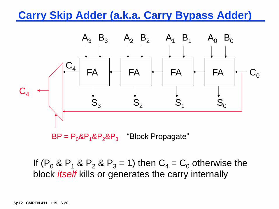
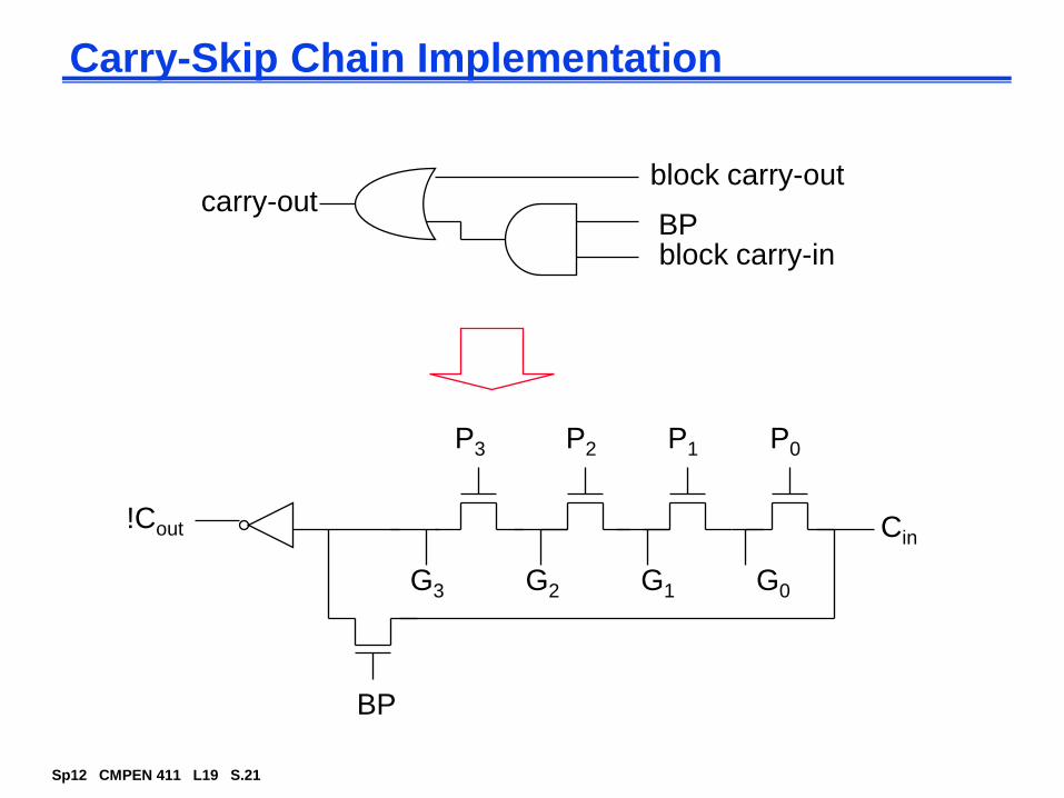
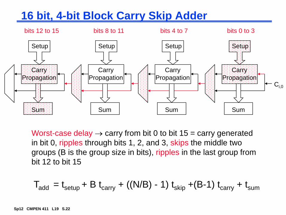
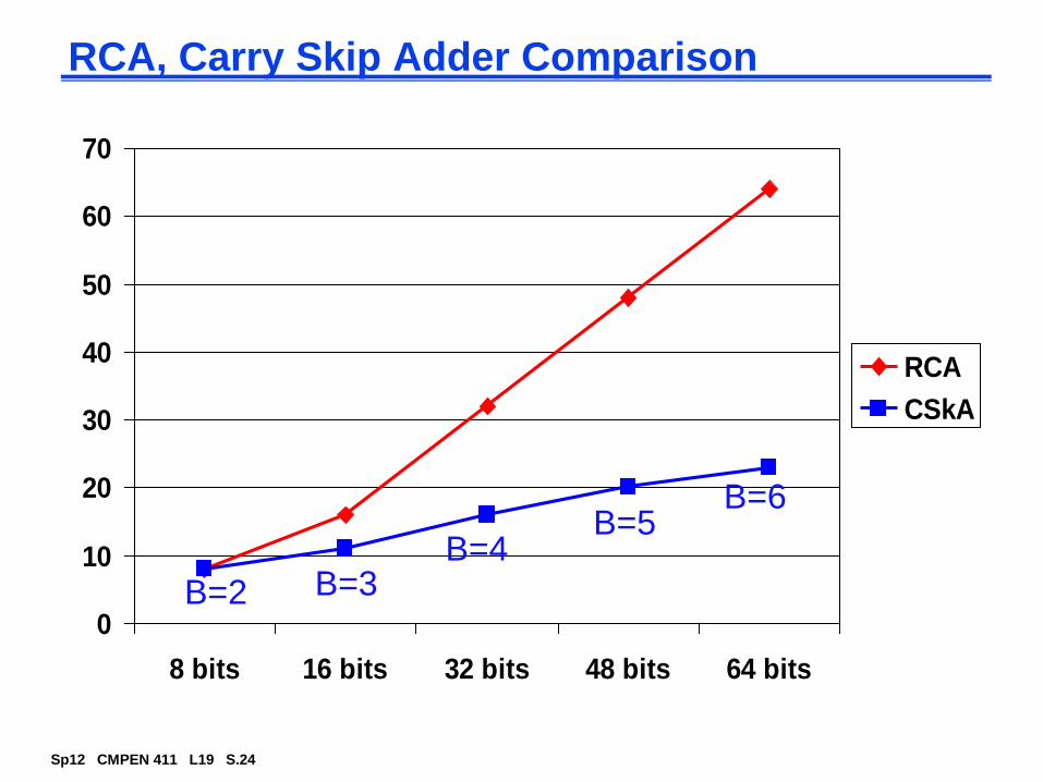
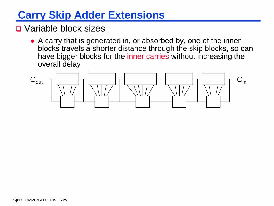
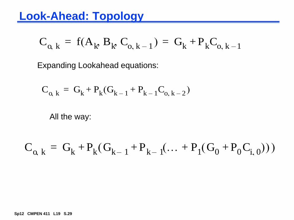
Fast Carry Chain Design
The key to fast addition is a low latency carry network
What matters is whether in a given position a carry is
A carry that is generated in, or absorbed by, one of the inner blocks travels a shorter distance through the skip blocks, so can have bigger blocks for the inner carries without increasing the overall delay
CinCout
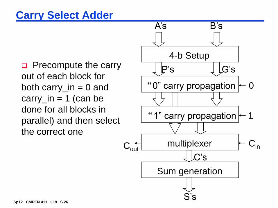
Sp12 CMPEN 411 L19 S.26
Carry Select Adder
4-b Setup
“0” carry propagation
“1” carry propagation 1
0
multiplexer CinCout
Sum generation
P’s G’s
C’s
Precompute the carry
out of each block for
both carry_in = 0 and
carry_in = 1 (can be
done for all blocks in
parallel) and then select
the correct one
A’s B’s
S’s
Sp12 CMPEN 411 L19 S.27
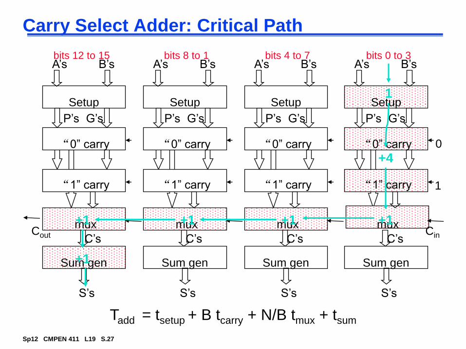
Carry Select Adder: Critical Path
Setup
“0” carry
“1” carry 1
0
muxCin
Sum gen
P’s G’s
C’s
S’s
A’s B’s
Setup
“0” carry
“1” carry
mux
Sum gen
P’s G’s
C’s
S’s
A’s B’s
Setup
“0” carry
“1” carry
mux
Sum gen
P’s G’s
C’s
S’s
A’s B’s
Setup
“0” carry
“1” carry
muxCout
Sum gen
P’s G’s
C’s
S’s
A’s B’sbits 0 to 3bits 4 to 7bits 8 to 1bits 12 to 15
Tadd = tsetup + B tcarry + N/B tmux + tsum
1
+4
+1+1+1+1
+1
Sp12 CMPEN 411 L19 S.28
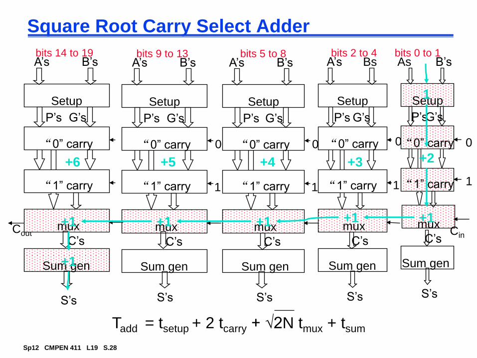
Square Root Carry Select Adder
Setup
“0” carry
“1” carry 1
0
muxCin
Sum gen
P’sG’s
C’s
S’s
As B’sA’s Bs
1
0
S’s
Setup
“0” carry
“1” carry
mux
Sum gen
P’s G’s
C’s
A’s B’s
Setup
“0” carry
“1” carry 1
0
muxCout
Sum gen
P’s G’s
C’s
S’s
A’s B’sbits 0 to 1bits 2 to 4bits 5 to 8bits 9 to 13