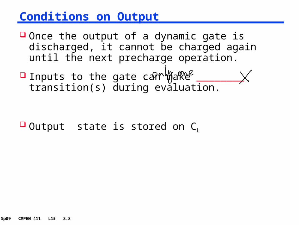
Once the output of a dynamic gate is discharged, it cannot be charged again until the next precharge operation.
Inputs to the gate can make ________ transition(s) during evaluation.
Output state is stored on CL
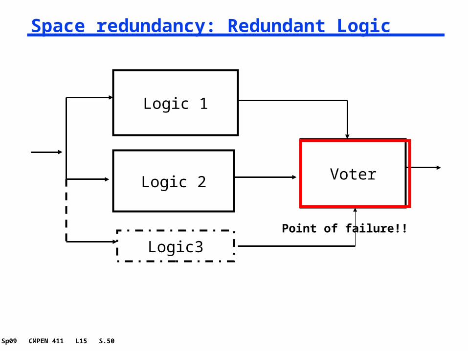
Sp09 CMPEN 411 L15 S.9
Properties of Dynamic Gates Logic function is implemented by the PDN only
number of transistors is _____(versus 2N for static complementary CMOS)
should be smaller in area than static complementary CMOS
Full swing outputs (VOL = GND and VOH = VDD)
Non-ratioed - sizing of the devices is not important for proper functioning (only for performance)
Faster switching speeds reduced load capacitance due to lower number of transistors per
gate (Cint) so a reduced logical effort reduced load capacitance due to smaller fan-out (Cext) no Isc, so all the current provided by PDN goes into discharging CL
Ignoring the influence of precharge time on the switching speed of the gate, tpLH = 0 but the presence of the evaluation transistor slows down the tpHL
Sp09 CMPEN 411 L15 S.10
Properties of Dynamic Gates, con’t Power dissipation should be lower
no ______________power consumption since the pull-up path is not on when evaluating
lower ____________- both Cint (since there are fewer transistors connected to the drain output) and Cext (since there the output load is one per connected gate, not two)
by construction can have at most one transition per cycle – no _______________
But power dissipation can be significantly higher due to _______________________ extra load on ____________
Needs a precharge clock
Sp09 CMPEN 411 L15 S.11
Dynamic Behavior
-0.5
0.5
1.5
2.5
0 0.5 1
CLK
CLK
In1
In2
In3
In4
Out
In &CLK
Out
Time, ns
Vol
tage
#Trns VOH VOL VM NMH NML tpHL tpLH tpre
6 2.5V 0V VTn 2.5-VTn VTn110ps 0ns 83ps
Evaluate
Precharge
Sp09 CMPEN 411 L15 S.13
Power Consumption of Dynamic Gate
In1
In2 PDN
In3
Me
Mp
CLK
CLK
Out
CL
Power only dissipated when previous Out = 0
Sp09 CMPEN 411 L15 S.14
Dynamic Power Consumption is Data Dependent
A B Out
0 0 1
0 1 0
1 0 0
1 1 0
Dynamic 2-input NOR Gate
Assume signal probabilities PA=1 = 1/2 PB=1 = 1/2
Then transition probability P01 = Pout=0 x Pout=1
= ___________
Switching activity can be higher in dynamic gates!P01 =__________
Sp09 CMPEN 411 L15 S.15
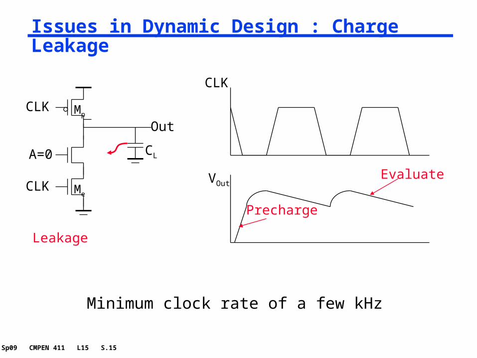
Issues in Dynamic Design : Charge Leakage
CL
CLK
CLK
Out
A=0
Mp
Me
Minimum clock rate of a few kHz
Leakage
CLK
VOut
Precharge
Evaluate
Sp09 CMPEN 411 L15 S.17
Impact of Charge Leakage Output settles to an intermediate voltage determined by
a resistive divider of the pull-up and pull-down networks Once the output drops below the switching threshold of the
fan-out logic gate, the output is interpreted as a low voltage.
-0.5
0.5
1.5
2.5
0 20 40
Time (ms)
Volta
ge (V
)
CLK
Out
Sp09 CMPEN 411 L15 S.18
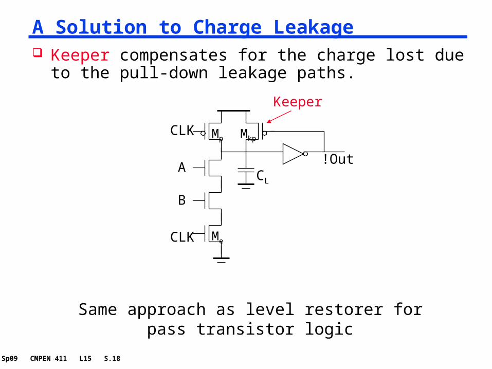
A Solution to Charge Leakage
CL
CLK
CLK
Me
Mp
A
B
!Out
Mkp
Same approach as level restorer for pass transistor logic
Keeper
Keeper compensates for the charge lost due to the pull-down leakage paths.
Sp09 CMPEN 411 L15 S.19
Issues in Dynamic Design : Charge Sharing
CL
CLK
CLK
Ca
Cb
B=0
A
OutMp
Me
Charge stored originally on CL is redistributed (shared) over CL and CA leading to static power consumption by downstream gates and possible circuit malfunction.
When Vout = - VDD (Ca / (Ca + CL )) the drop in Vout is large enough to be below the switching threshold of the gate it drives causing a malfunction.
Sp09 CMPEN 411 L15 S.22
Solution to Charge Redistribution
CLK
CLK
Me
Mp
A
B
OutMkp
CLK
Precharge internal nodes using a clock-driven transistor (at the cost of increased area and power)
Sp09 CMPEN 411 L15 S.27
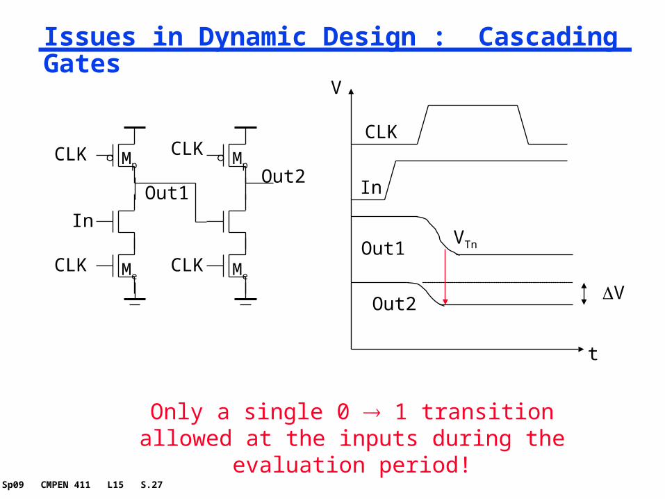
Issues in Dynamic Design : Cascading Gates
CLK
CLK
Out1
In
Mp
Me
Mp
Me
CLK
CLK
Out2
V
t
CLK
In
Out1
Out2V
VTn
Only a single 0 1 transition allowed at the inputs during the evaluation period!
Sp09 CMPEN 411 L15 S.28
Domino Logic
In1
In2 PDN
In3
Me
Mp
CLK
CLKOut1
In4 PDN
In5
Me
Mp
CLK
CLKOut2
Mkp
1 11 0
0 00 1
Sp09 CMPEN 411 L15 S.29
Why Domino?
In1
CLK
CLK
Ini PDNInj
Ini
Inj
PDN Ini PDNInj
Ini PDNInj
Like falling dominos!
Sp09 CMPEN 411 L15 S.31
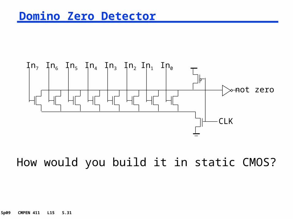
Domino Zero Detector
CLK
In7 In6 In5 In4 In3 In2 In0In1
not zero
How would you build it in static CMOS?
Sp09 CMPEN 411 L15 S.33
Properties of Domino Logic
Only non-inverting logic can be implemented, fixes include
can reorganize the logic using Boolean transformations use differential logic (dual rail) use np-CMOS (zipper)
Very high speed tpHL = 0 static inverter can be optimized to match fan-out (separation of
fan-in and fan-out capacitances)
Sp09 CMPEN 411 L15 S.34
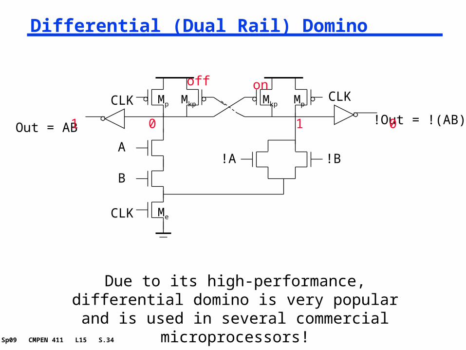
Differential (Dual Rail) Domino
A
B
Me
Mp
CLK
CLK
!Out = !(AB)
!A !B
MkpCLK
Out = AB
Mkp Mp
Due to its high-performance, differential domino is very popular and is used in several commercial
microprocessors!
1 0 1 0
onoff
Sp09 CMPEN 411 L15 S.35
Other Domino Variations
Multiple output domino logic – exploits the fact that certain outputs are subsets of other outputs to generate a number of logic functions in a single gate.
Compound domino
A
B
Me
Mp
CLK
CLK
C
D
E
MeCLK
F
MpCLK
G
Me
H
Mp
Sp09 CMPEN 411 L15 S.36
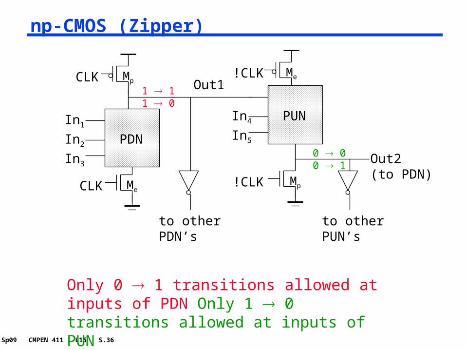
np-CMOS (Zipper)
In1
In2 PDN
In3
Me
Mp
CLK
CLKOut1
In4 PUN
In5
Me
Mp!CLK
!CLK
Out2(to PDN)
1 11 0
0 00 1
Only 0 1 transitions allowed at inputs of PDN Only 1 0 transitions allowed at inputs of PUN
to otherPDN’s
to otherPUN’s
Sp09 CMPEN 411 L15 S.39
DCVS Logic (Differential Cascade Voltage Switch
In1
In2
PDN1
Out
!In1
!In2
PDN2
!Out
PDN1 and PDN2 are mutually exclusive
1 0 0on off
off on on off
on off 1
Sp09 CMPEN 411 L15 S.40
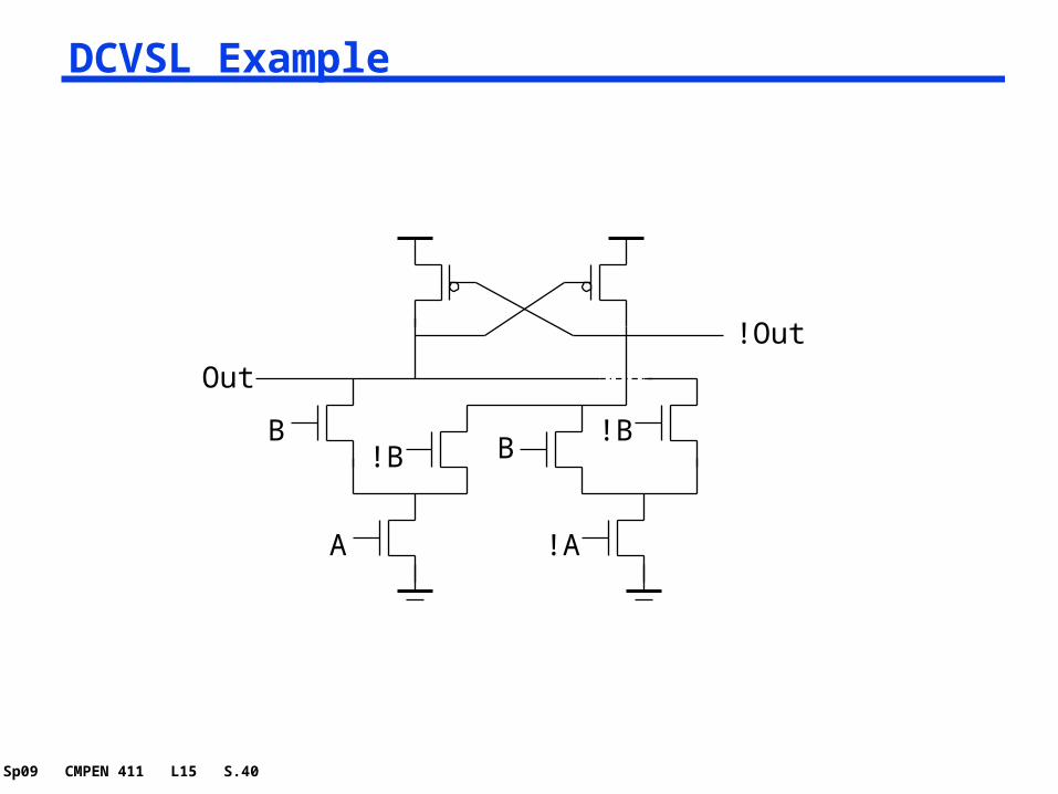
DCVSL Example
Out
!Out
B
A !A
B!B!B
Sp09 CMPEN 411 L15 S.41
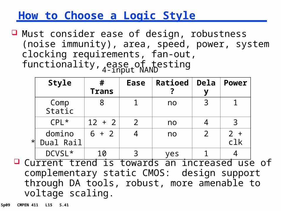
How to Choose a Logic Style
Must consider ease of design, robustness (noise immunity), area, speed, power, system clocking requirements, fan-out, functionality, ease of testing
Style # Trans Ease Ratioed? Delay Power
Comp Static 8 1 no 3 1
CPL* 12 + 2 2 no 4 3
domino 6 + 2 4 no 2 2 + clk
DCVSL* 10 3 yes 1 4
4-input NAND
* Dual Rail
Current trend is towards an increased use of complementary static CMOS: design support through DA tools, robust, more amenable to voltage scaling.
Sp09 CMPEN 411 L15 S.42
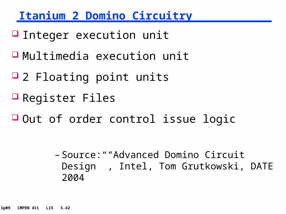
Itanium 2 Domino Circuitry
Integer execution unit
Multimedia execution unit
2 Floating point units
Register Files
Out of order control issue logic
– Source: “Advanced Domino Circuit Design” , Intel, Tom Grutkowski, DATE 2004
Sp09 CMPEN 411 L15 S.43
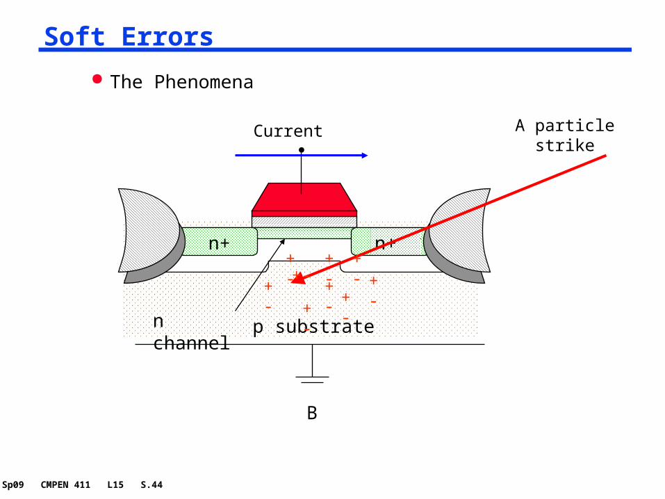
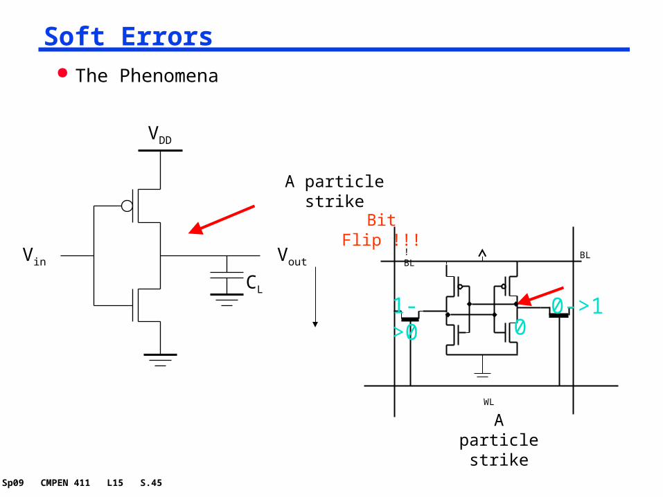
What is Soft Error
Soft errors are circuit errors caused due to excess charge carriers induced primarily by external radiations
These errors cause an upset event but the circuit it self is not damaged.
Same a SEU (single event upset)
Sp09 CMPEN 411 L15 S.44
B
p substrate
G
n+n+
n channel
Soft Errors
The Phenomena
+ - + -+ -
+ -+-
+ -+ -
+ -+ -
A particle strikeCurrent
Sp09 CMPEN 411 L15 S.45
Soft Errors The Phenomena
VDD
Vout
CL
Vin
A particle strike
Bit Flip !!!
A particle strike
!BL
BL
WL
0->11->0 0
Sp09 CMPEN 411 L15 S.46
What cause Soft Errors?
At ground level, there are three major contributors to Soft errors.
1. Cosmic Ray induced neutrons
2. Alpha particles emitted by decaying radioactive impurities in packaging or interconnect materials.
3. Neutron induced 10B fission which releases a Alpha particle and 7Li
Sp09 CMPEN 411 L15 S.47
Evidence of Cosmic Ray Strikes
Documented strikes in large servers found in error logs Normand, “Single Event Upset at Ground Level,” IEEE Transactions
on Nuclear Science, Vol. 43, No. 6, December 1996.
Sun Microsystems, 2000 Cosmic ray strikes on L2 cache with no error detection or correction
- caused Sun’s flagship servers to suddenly and mysteriously crash!
Companies affected
- Baby Bell (Atlanta), America Online, Ebay, & dozens of other corporations
- Verisign moved to IBM Unix servers (for the most part)
Sp09 CMPEN 411 L15 S.48
Reactions from Companies
Fujitsu SPARC in 130 nm technology 80% of 200k latches protected with parity compare with very few latches protected in Mckinley ISSCC, 2003
IBM declared 1000 years system MTBF as product goal very hard to achieve this goal in a cost-effective way