Timing issues, Intro to datapath design- Reading assignment – Rabaey, et al, 10.1-10.3.3; 11.1-11.2
Next lecture Intro to datapath design
- Reading assignment – Rabaey, et al, 11.1-11.2
Adder design- Reading assignment – Rabaey, et al, 11.3
Sp09 CMPEN 411 L17 S.3
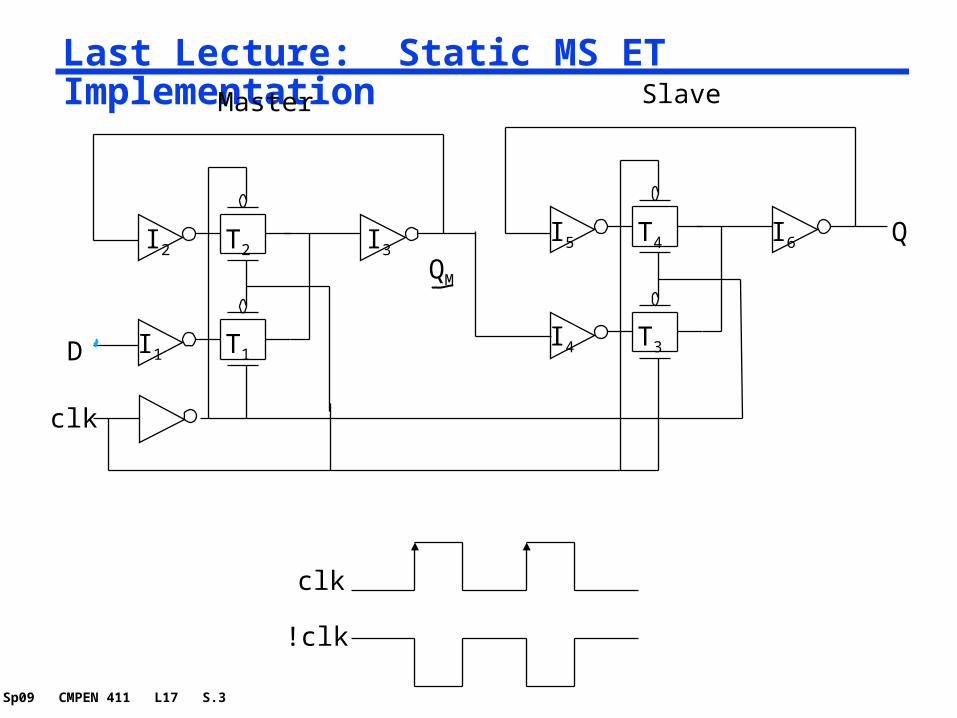
Last Lecture: Static MS ET Implementation
Q
D
clk
QM
I1
I2 I3
I4
I5 I6T2
T1T3
T4
Master Slave
!clk
clk
Sp09 CMPEN 411 L17 S.4
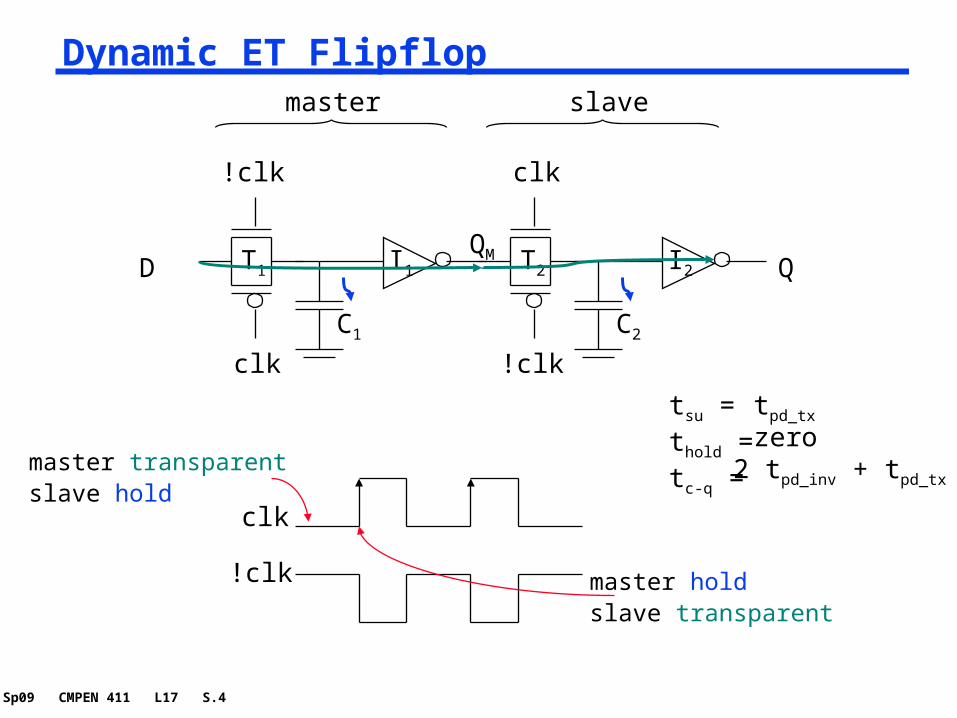
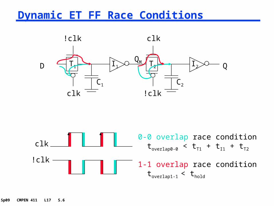
Dynamic ET Flipflop
T1 T2I1 I2 QQM
D
C1 C2
!clk
clk
clk
!clk
!clk
clk
master transparentslave hold
master holdslave transparent
master slave
tsu =thold =tc-q =
tpd_tx
zero2 tpd_inv + tpd_tx
Sp09 CMPEN 411 L17 S.5
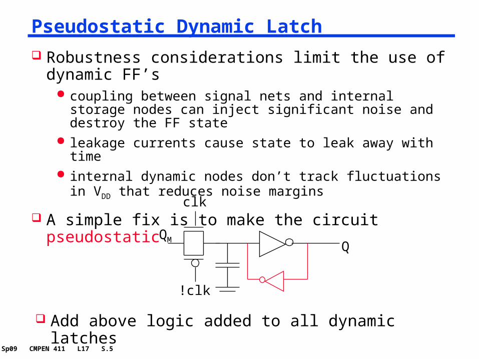
Pseudostatic Dynamic Latch
Robustness considerations limit the use of dynamic FF’s coupling between signal nets and internal storage nodes can
inject significant noise and destroy the FF state leakage currents cause state to leak away with time internal dynamic nodes don’t track fluctuations in VDD that
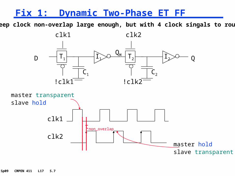
Keep clock non-overlap large enough, but with 4 clock singals to route
Sp09 CMPEN 411 L17 S.8
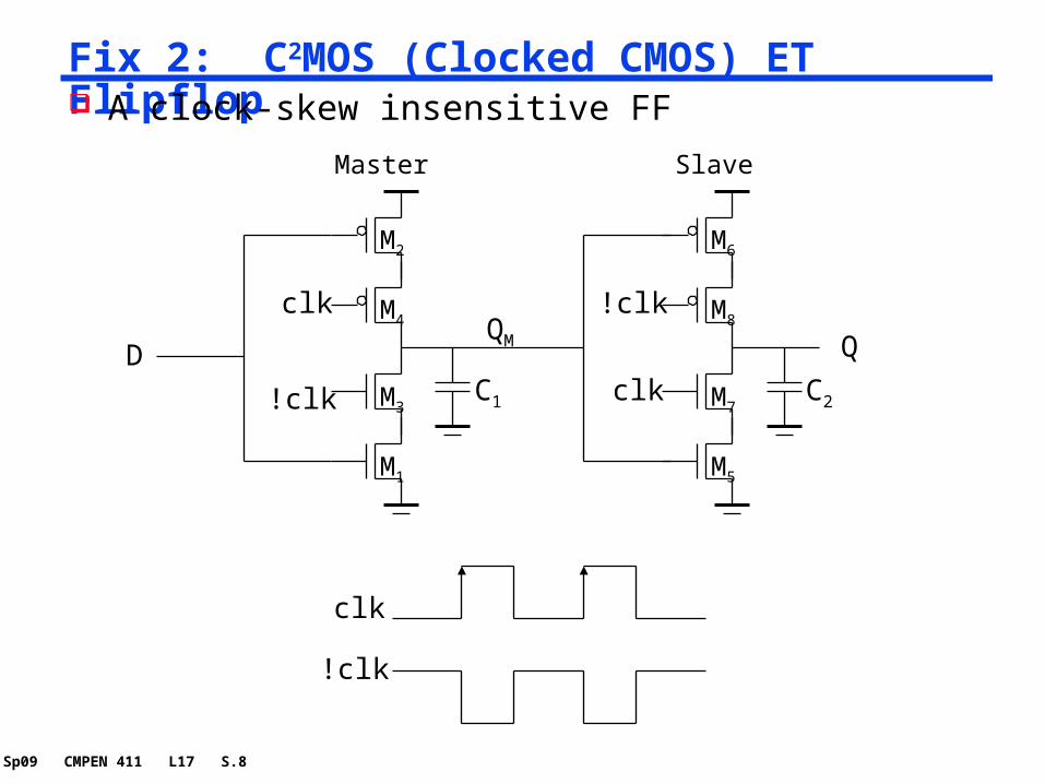
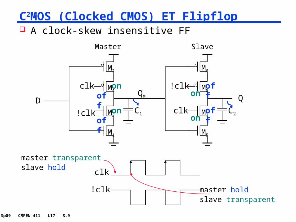
Fix 2: C2MOS (Clocked CMOS) ET Flipflop
clk
!clk
!clk
clk
QM
C1 C2
QD
M1
M3
M4
M2 M6
M8
M7
M5
Master Slave
!clk
clk
A clock-skew insensitive FF
Sp09 CMPEN 411 L17 S.9
C2MOS (Clocked CMOS) ET Flipflop
clk
!clk
!clk
clk
QM
C1 C2
QD
M1
M3
M4
M2 M6
M8
M7
M5
Master Slave
!clk
clk
master transparentslave hold
master holdslave transparent
on
on
off
offon
onoff
off
A clock-skew insensitive FF
Sp09 CMPEN 411 L17 S.10
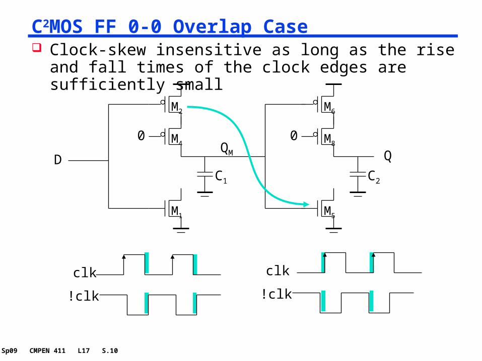
C2MOS FF 0-0 Overlap Case
0 0QM
C1 C2
QD
M1
M4
M2 M6
M8
M5
!clk
clk
!clk
clk
Clock-skew insensitive as long as the rise and fall times of the clock edges are sufficiently small
Sp09 CMPEN 411 L17 S.11
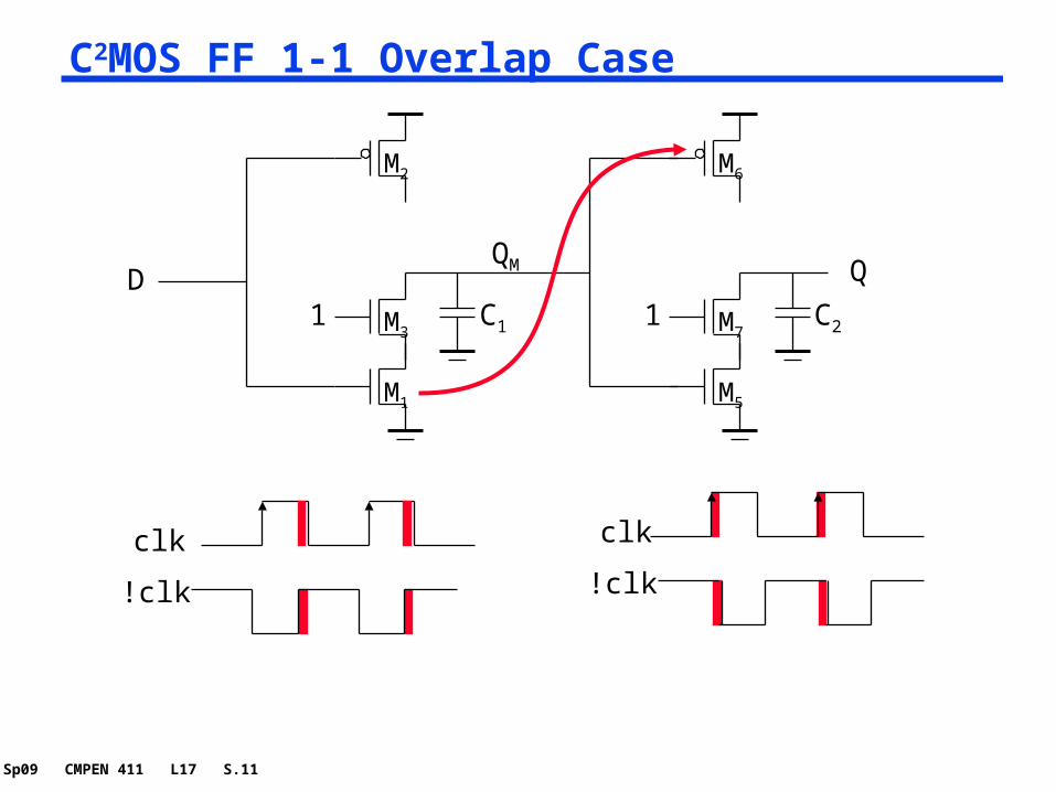
C2MOS FF 1-1 Overlap Case
1 1
QM
C1 C2
QD
M1
M2 M6
M5
!clk
clk
M3 M7
!clk
clk
Sp09 CMPEN 411 L17 S.12
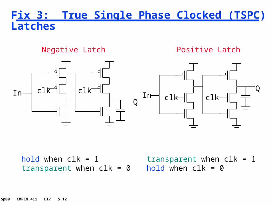
Fix 3: True Single Phase Clocked (TSPC) Latches
clk clkInQ
Positive LatchNegative Latch
transparent when clk = 1hold when clk = 0
clk clkInQ
hold when clk = 1transparent when clk = 0
Sp09 CMPEN 411 L17 S.13
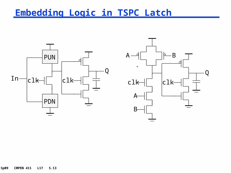
Embedding Logic in TSPC Latch
clk clkInQ
PUN
PDN
clk clk
A
Q
B
BA
Sp09 CMPEN 411 L17 S.14
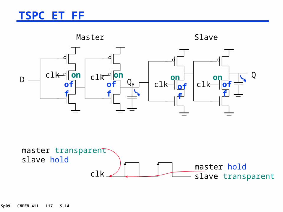
TSPC ET FF
clkmaster holdslave transparent
clk clkD
Master Slave
clk clk QQM
master transparentslave hold
ononoffoff
ononoffoff
on onoffoff
Sp09 CMPEN 411 L17 S.15
Choosing a Clocking Strategy
Choosing the right clocking scheme affects the functionality, speed, and power of a circuit
Two-phase designs + robust and conceptually simple - need to generate and route two clock signals - have to design to accommodate possible skew between the
two clock signals
Single phase designs + only need to generate and route one clock signal + supported by most automated design methodologies + don’t have to worry about skew between the two clocks - have to have guaranteed slopes on the clock edges
Sp09 CMPEN 411 L17 S.16
Review: Sequential Definitions
Use two, level sensitive latches of opposite type to build one master-slave flipflop that changes state on a clock edge (when the slave is transparent)
Static storage static uses a bistable element with feedback to store its state and
thus preserves state as long as the power is on- Loading new data into the element: 1) cutting the feedback path (mux
based); 2) overpowering the feedback path (SRAM based)
Dynamic storage dynamic stores state on parasitic capacitors so the state held for
only a period of time (milliseconds); requires periodic refresh dynamic is usually simpler (fewer transistors), higher speed, lower
power but due to noise immunity issues always modify the circuit (by adding a feedback loop on the output) so that it is pseudostatic
Sp09 CMPEN 411 L17 S.17
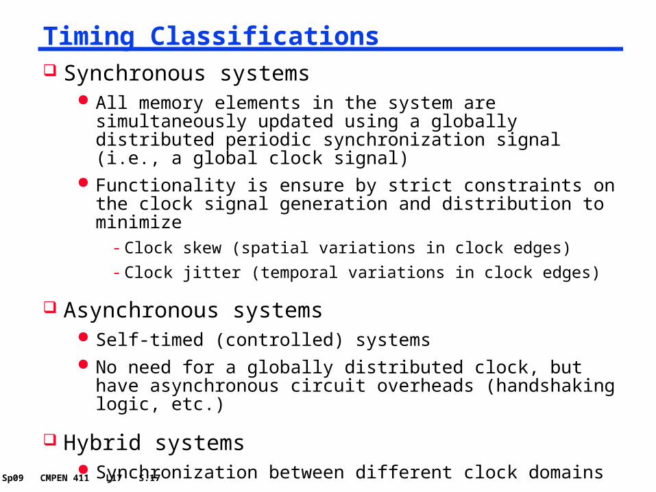
Timing Classifications Synchronous systems
All memory elements in the system are simultaneously updated using a globally distributed periodic synchronization signal (i.e., a global clock signal)
Functionality is ensure by strict constraints on the clock signal generation and distribution to minimize
- Clock skew (spatial variations in clock edges)
- Clock jitter (temporal variations in clock edges)
Asynchronous systems Self-timed (controlled) systems No need for a globally distributed clock, but have asynchronous
circuit overheads (handshaking logic, etc.)
Hybrid systems Synchronization between different clock domains Interfacing between asynchronous and synchronous domains
Sp09 CMPEN 411 L17 S.18
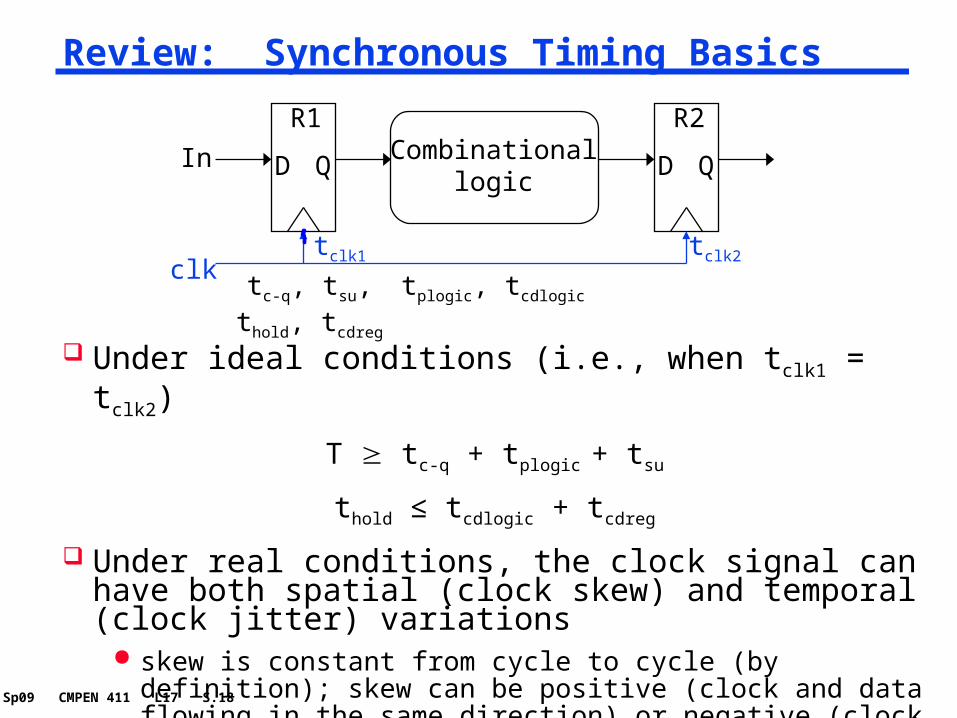
Review: Synchronous Timing Basics
Under ideal conditions (i.e., when tclk1 = tclk2)
T tc-q + tplogic + tsu
thold ≤ tcdlogic + tcdreg
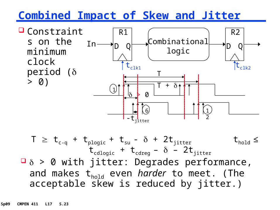
Under real conditions, the clock signal can have both spatial (clock skew) and temporal (clock jitter) variations
skew is constant from cycle to cycle (by definition); skew can be positive (clock and data flowing in the same direction) or negative (clock and data flowing in opposite directions)
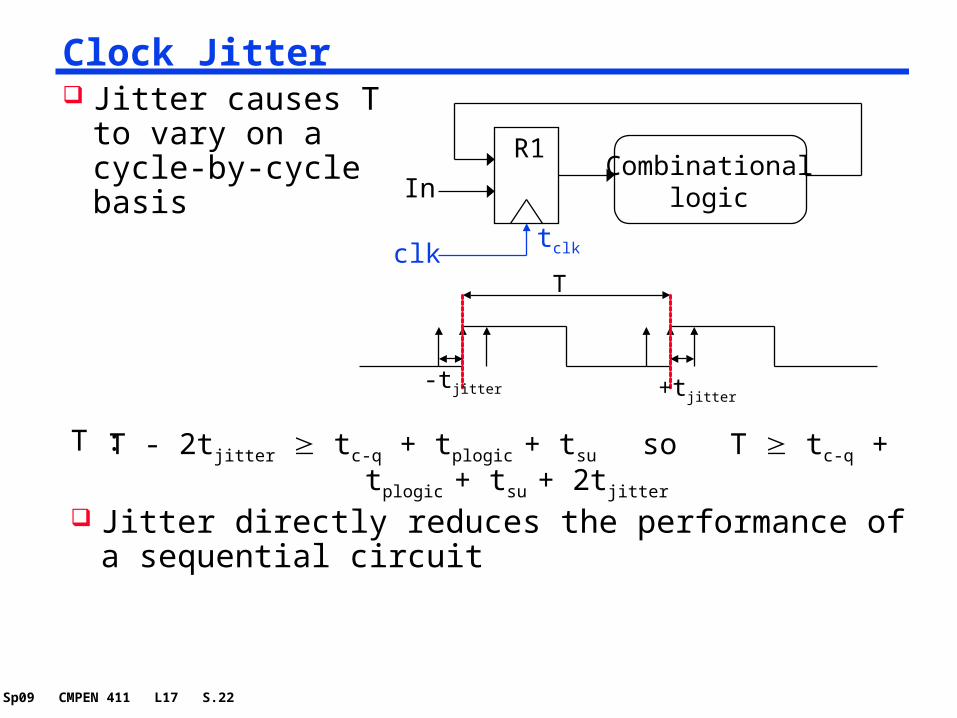
jitter causes T to change on a cycle-by-cycle basis
D Q
R1Combinational
logicD Q
R2
clk
In
tclk1 tclk2
tc-q, tsu,thold, tcdreg
tplogic, tcdlogic
Sp09 CMPEN 411 L17 S.19
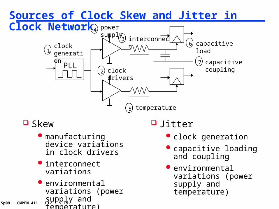
Sources of Clock Skew and Jitter in Clock Network
PLL
1
2
4
3
5
6
7
clock generation
clock drivers
power supply
interconnectcapacitive load
capacitive coupling
temperature
Skew manufacturing device
variations in clock drivers interconnect variations environmental variations
(power supply and temperature)
Jitter clock generation capacitive loading and
coupling environmental variations
(power supply and temperature)
Sp09 CMPEN 411 L17 S.20
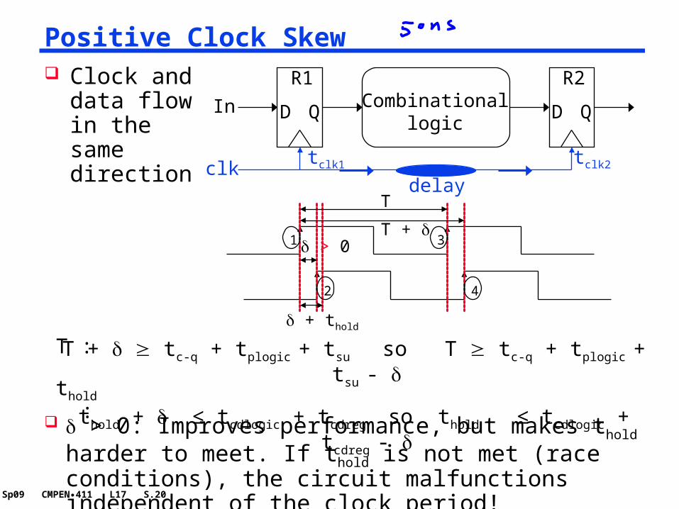
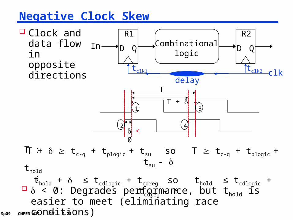
Positive Clock Skew
D Q
R1Combinational
logicD Q
R2
clk
In
tclk1 tclk2
delay
> 0: Improves performance, but makes thold harder to meet. If thold is not met (race conditions), the circuit malfunctions independent of the clock period!
T
T + > 0
+ thold
T + tc-q + tplogic + tsu so T tc-q + tplogic + tsu -
Clock skew and jitter can ultimately limit the performance of a digital system, so designing a clock network that minimizes both is important
In many high-speed processors, a majority of the dynamic power is dissipated in the clock network.
To reduce dynamic power, the clock network must support clock gating (shutting down (disabling the clock) units)
Clock distribution techniques Balanced paths (H-tree network, matched RC trees)
- In the ideal case, can eliminate skew
- Could take multiple cycles for the clock signal to propagate to the leaves of the tree
Clock grids- Typically used in the final stage of the clock distribution network
- Minimizes absolute delay (not relative delay)
Sp09 CMPEN 411 L17 S.25
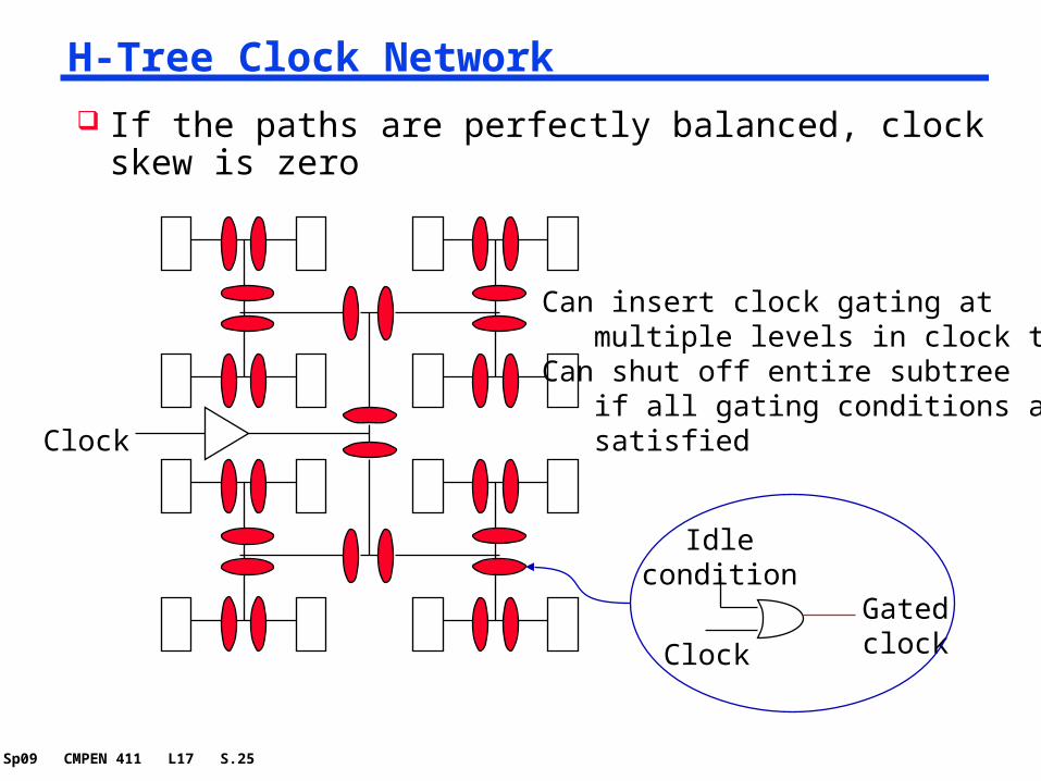
H-Tree Clock Network
Clock
Clock
Idlecondition
Gatedclock
Can insert clock gating at multiple levels in clock treeCan shut off entire subtree if all gating conditions are satisfied
If the paths are perfectly balanced, clock skew is zero
Sp09 CMPEN 411 L17 S.26
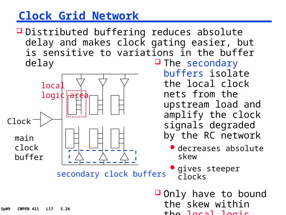
Clock Grid Network Distributed buffering reduces absolute delay and makes
clock gating easier, but is sensitive to variations in the buffer delay
Clock
secondary clock buffers
local logic area
main clock buffer
The secondary buffers isolate the local clock nets from the upstream load and amplify the clock signals degraded by the RC network
decreases absolute skew gives steeper clocks
Only have to bound the skew within the local logic area
Sp09 CMPEN 411 L17 S.27
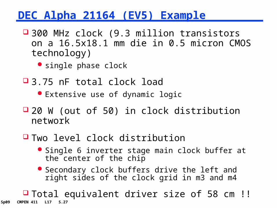
DEC Alpha 21164 (EV5) Example
300 MHz clock (9.3 million transistors on a 16.5x18.1 mm die in 0.5 micron CMOS technology)
single phase clock
3.75 nF total clock load Extensive use of dynamic logic
20 W (out of 50) in clock distribution network
Two level clock distribution Single 6 inverter stage main clock buffer at the center of the
chip Secondary clock buffers drive the left and right sides of the
clock grid in m3 and m4
Total equivalent driver size of 58 cm !!
Sp09 CMPEN 411 L17 S.28
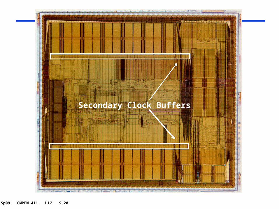
Secondary Clock Buffers
Sp09 CMPEN 411 L17 S.29
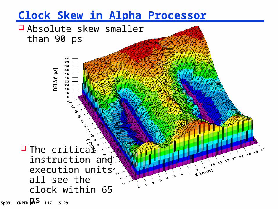
Clock Skew in Alpha Processor Absolute skew smaller than 90 ps
The critical instruction and execution units all see the clock within 65 ps
Sp09 CMPEN 411 L17 S.30
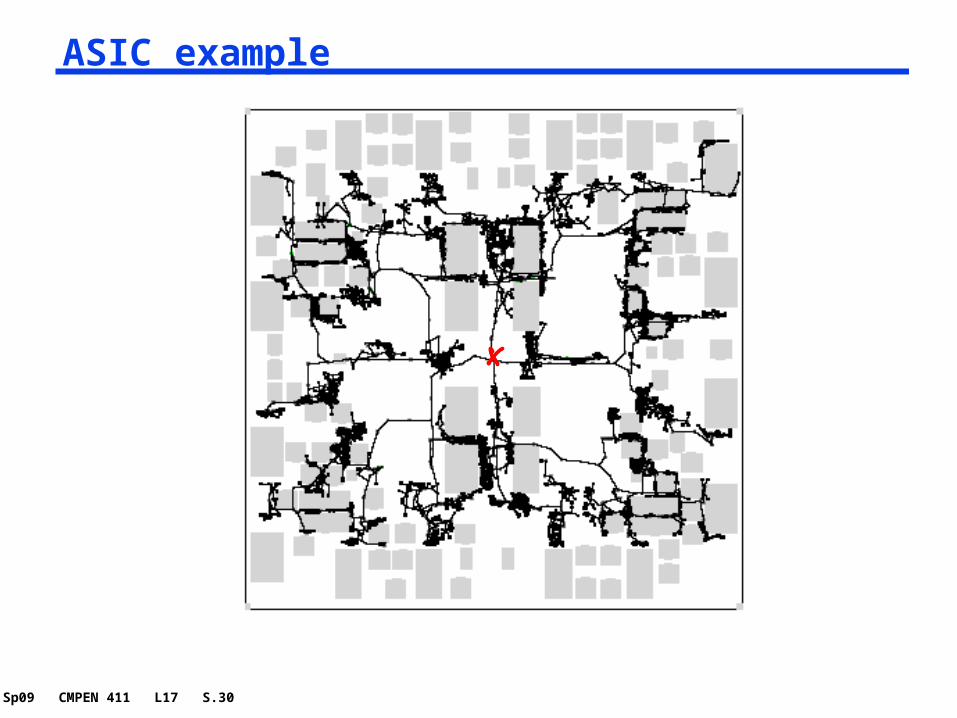
ASIC example
Sp09 CMPEN 411 L17 S.31
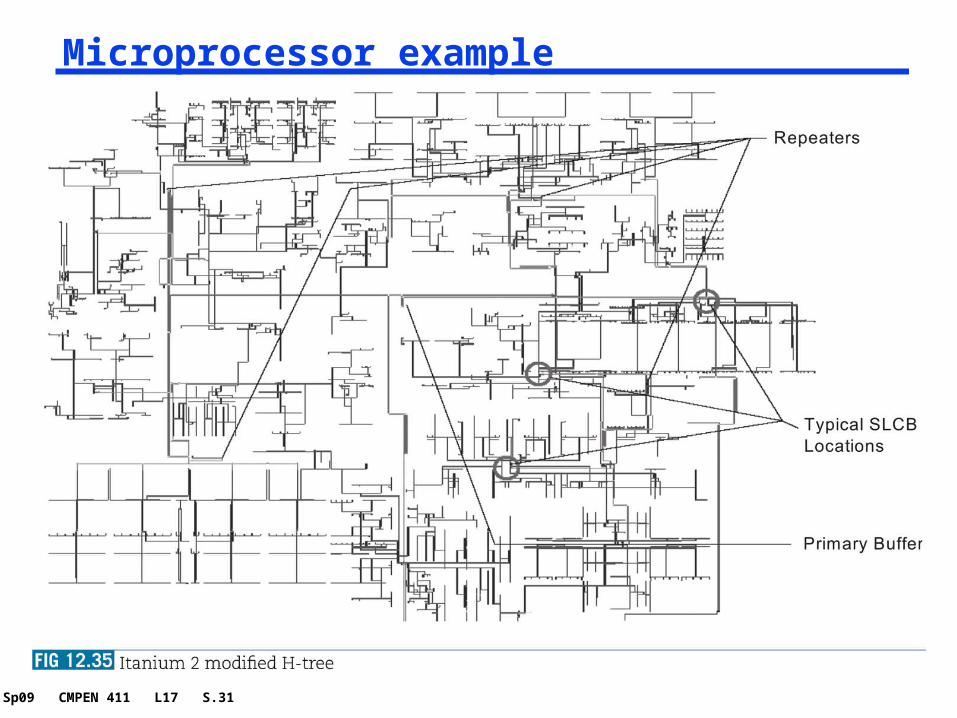
Microprocessor example
Sp09 CMPEN 411 L17 S.32
Dealing with Clock Skew and Jitter To minimize skew, balance clock paths using H-tree or
matched-tree clock distribution structures.
If possible, route data and clock in opposite directions; eliminates races at the cost of performance.
The use of gated clocks to help with dynamic power consumption make jitter worse.
Shield clock wires (route power lines – VDD or GND – next to clock lines) to minimize/eliminate coupling with neighboring signal nets.
Use dummy fills to reduce skew by reducing variations in interconnect capacitances due to interlayer dielectric thickness variations.
Beware of temperature and supply rail variations and their effects on skew and jitter. Power supply noise fundamentally limits the performance of clock networks.
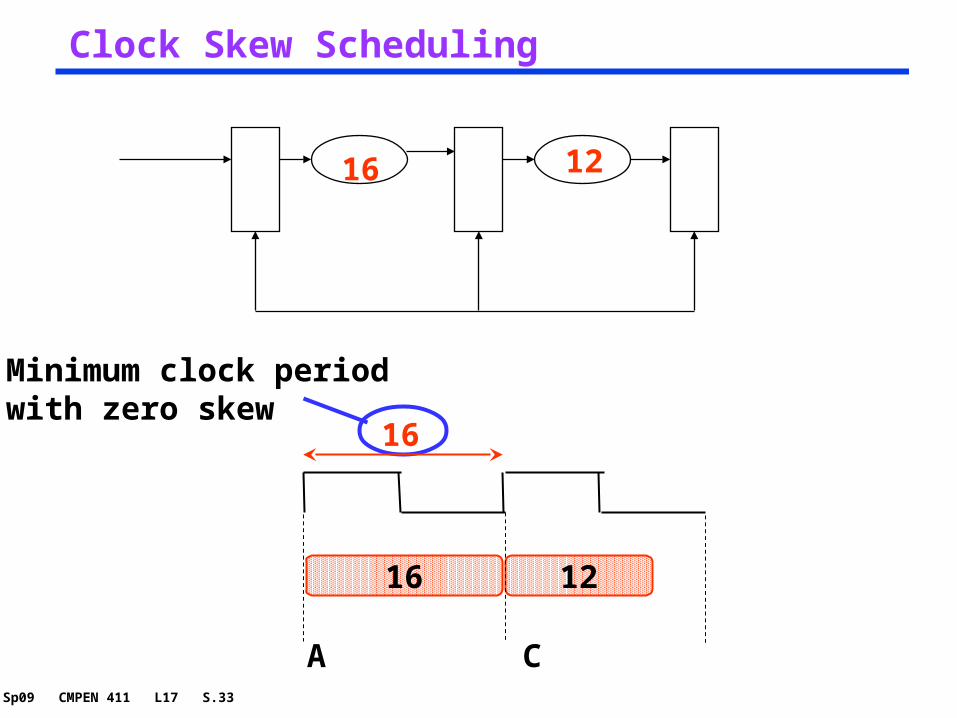
Sp09 CMPEN 411 L17 S.33
Clock Skew Scheduling
16
1216
A C
Minimum clock periodwith zero skew
16 12
Sp09 CMPEN 411 L17 S.34
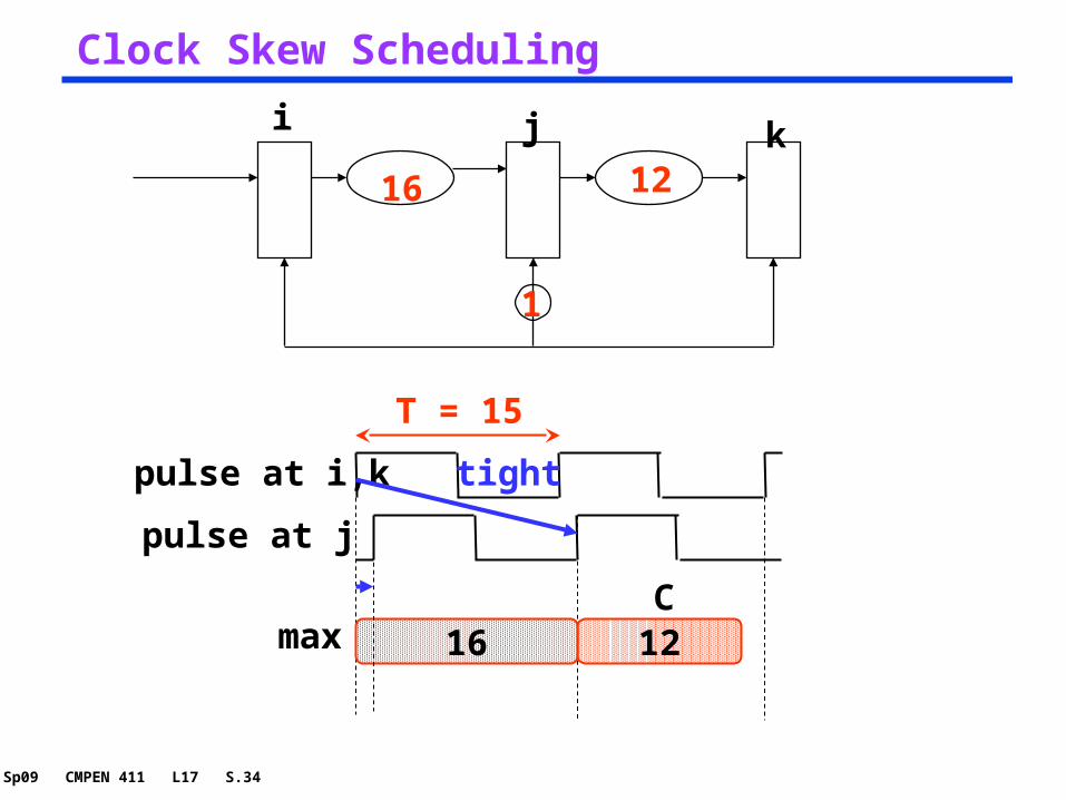
Clock Skew Scheduling
16 12
C12max 16
pulse at i,k
pulse at j
T = 15
tight
i j k
1
Sp09 CMPEN 411 L17 S.35
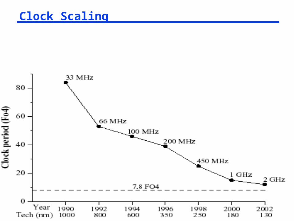
Clock Scaling
Sp09 CMPEN 411 L17 S.36
Next Lecture and Reminders Next lecture
Intro to datapath design- Reading assignment – Rabaey, et al, 11.1-11.2
Adder design- Reading assignment – Rabaey, et al, 11.3