Guide to the CMPEN 411 Lab and Cad tools 1. Introduction The objective of this tutorial is to give you an overview to (1) setup the Cadence and Synopsys hspice tools for your account in IST 218 Lab, (2) use the schematic editor, (3) use the hspice tool, (3) use the chip layout editor - Cadence Virtuoso, and (4) use DRC, Extract, LVS tools. This guide may be updated as needed during the semester. 2. Set up the tool environment Before you can start using design tools, there are a few configuration files needed in your working directory. These files determine the environment in which tools run, and what libraries are to be included in your designs. The setup given below is for UNIX machines in Lab 218. Some UNIX commands will be included in this tutorial. Please be familiar with basic UNIX commands to work efficiently. Step1. Login to a machine in room 218 IST Building. Bring up a terminal window where you can type a UNIX command. Then type the following: % /home/faculty/kyusun/c411/bin/class411setup This setup needs to be done only once for this semester. Now for the setup to take effect, you logout and login again. Step 2. Make your own working directory for CMPEN 411 class. I made: % mkdir c411 The “c411” is the name of your working directory. You can use any name you like. Step3. Change your current directory to c411 by typing: % cd c411 You need to set up your directory for the CAD tool use. So type: % runcds This command needs to be done only once for this semester and all the subdirectories created by the Cadence tool is covered. (If you want to do your VLSI design in another directory later in the semester, you would need to “cd” to that directory and do “runcds” once for that directory.) Now start the Cadence tool by typing the following: % virtuoso & Then the CIW (Command Interpreter Window) and the library manager should pop up.
Transcript
Guide to the CMPEN 411 Lab and Cad tools 1. Introduction The objective of this tutorial is to give you an overview to (1) setup the Cadence and Synopsys hspice tools for your account in IST 218 Lab, (2) use the schematic editor, (3) use the hspice tool, (3) use the chip layout editor - Cadence Virtuoso, and (4) use DRC, Extract, LVS tools. This guide may be updated as needed during the semester.
2. Set up the tool environment Before you can start using design tools, there are a few configuration files needed in your working directory. These files determine the environment in which tools run, and what libraries are to be included in your designs. The setup given below is for UNIX machines in Lab 218. Some UNIX commands will be included in this tutorial. Please be familiar with basic UNIX commands to work efficiently.
Step1. Login to a machine in room 218 IST Building. Bring up a terminal window where you can type a UNIX command. Then type the following: % /home/faculty/kyusun/c411/bin/class411setup This setup needs to be done only once for this semester. Now for the setup to take effect, you logout and login again.
Step 2. Make your own working directory for CMPEN 411 class. I made: % mkdir c411 The “c411” is the name of your working directory. You can use any name you like.
Step3. Change your current directory to c411 by typing: % cd c411 You need to set up your directory for the CAD tool use. So type: % runcds This command needs to be done only once for this semester and all the subdirectories created by the Cadence tool is covered. (If you want to do your VLSI design in another directory later in the semester, you would need to “cd” to that directory and do “runcds” once for that directory.) Now start the Cadence tool by typing the following: % virtuoso & Then the CIW (Command Interpreter Window) and the library manager should pop up.
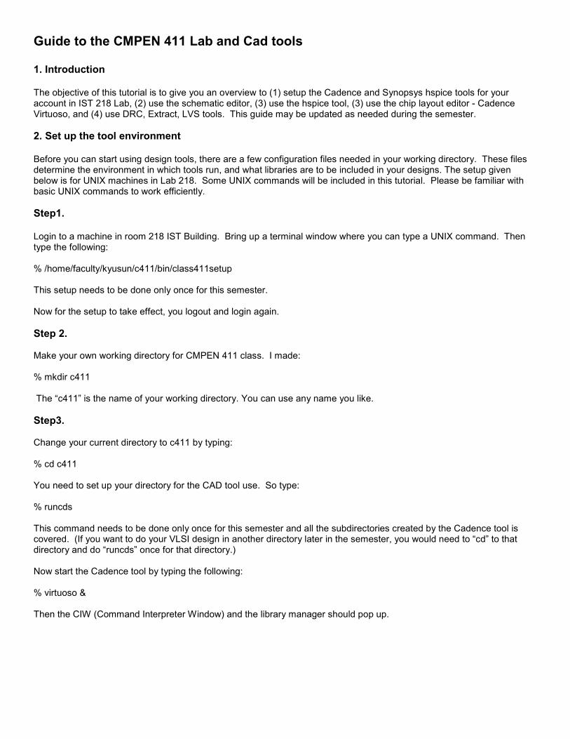
Figure 1a CIW Window
Figure 2b CIW Window with proper starting, Library Manager pops up
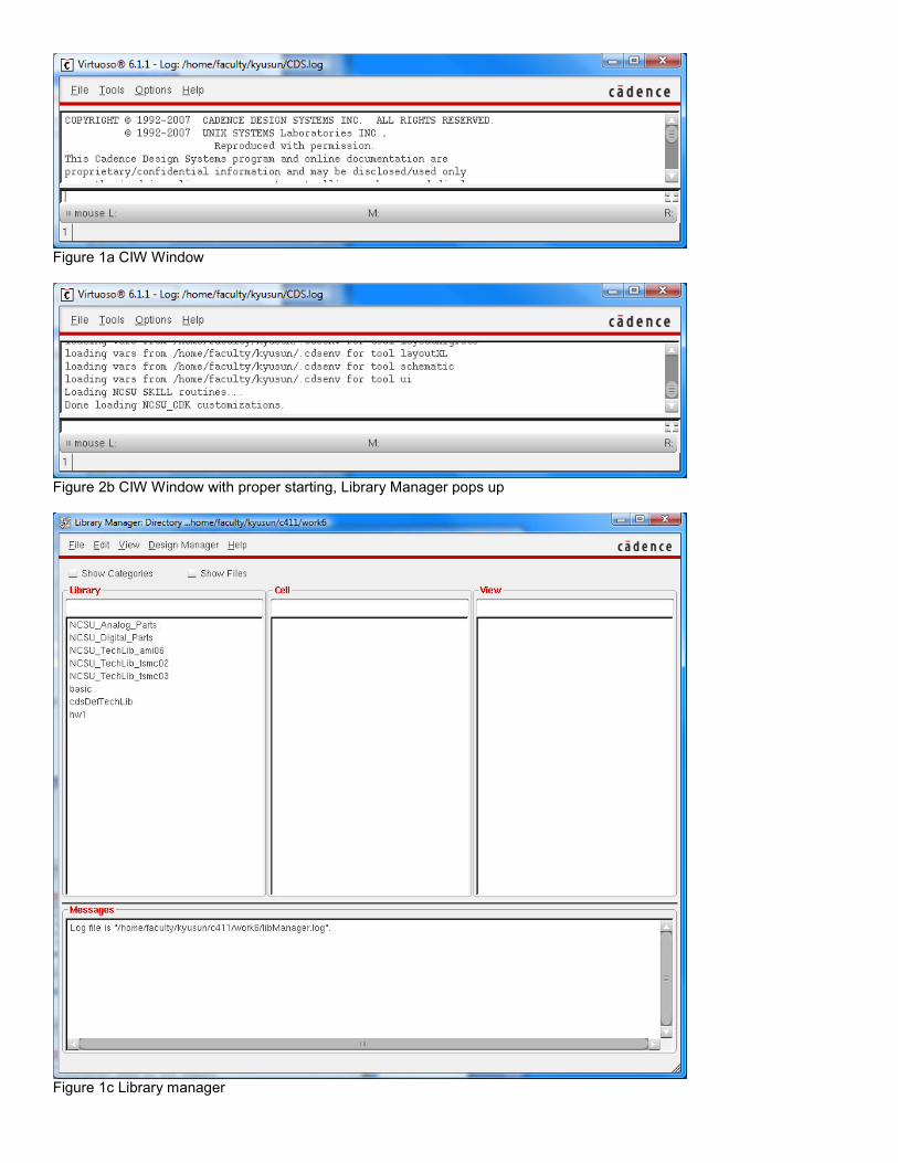
Figure 1c Library manager
Figure 3d CIW Window with NOT proper starting, Library Manager does NOT pops up If you see the Library Manager on your screen, your set up is proper. If you do NOT see the Library Manager and see the ‘*WARNING*’ message in CIW window, your set up is not proper, you can still use Cadence Virtuoso tool and do the work but you need to see the lab-support staffs in room 111 IST Building to update your account. You need to also send email to: [email protected]
Step4. Optional – connecting to the Lab 218 IST machines from home or campus You can connect to the Lab 218 IST machines from home Windows PC and do the VLSI design work at home. You will need the following: VPN - http:// downloads.its.psu.edu SSH - http:// downloads.its.psu.edu Plus you will need one of the following X11 clients running on your Windows PC: Xming Xmanager Xwin32 Exceed from Hummingbird cygwin Once you have the above programs installed on your Windows PC, follow the steps below to connect to the Lab 218 IST machines: Run VPN, set ‘ISP to PSU’ Run X11 client program Run ssh, login one of the following machines: alderaan drakh lumati romulan alphan drazi melmak scalosian andorian gallifrey metron taelon betazed gamalon minbari tamaria borg horta monikan tholian breen invid narn ubese cardassian kazon pakled venticar centauri klingon planet10 vogon cylon kronos protoss wookie degobah krypton raisa zerg
Double click on the ssh shell to start the ssh.
Click on the ‘Settings’ and be sure to check on the ‘Tunnel X11 connection’ as shown below.
Once the ssh shell started, click on ‘Quick Connect’ and type the followings, for example: Host Name: alderaan.cse.psu.edu User Name: your_cse_user_id Port Number: 22 Authentication Method: Password Once you are logged-in, type ‘xclock &’ to see if X11 is properly working. You will see a new clock on your screen. Otherwise X11 is not working.
3. Working with Cadence tool - virtuoso Using the Cadence tool, the overall VLSI chip design flow can be outlined as follows:
1. Schematic design and entry – transistors, symbols, input pins, output pins vdd pin, and gnd pin 2. Schematic check – check and save 3. Schematic spice netlist file creation 4. Hspice simulation of the netlist file from the schematic 5. Schematic symbol creation
6. Layout design and entry – pmos, nmos, ptap, NTAP, input pins, output pins, vdd! pin, and gnd! pin 7. Layout DRC (Design Rule Check) 8. Extraction of circuits from the layout including parasitic elements 9. Spice netlist file creation from the layout-extracted circuit 10. Hspice simulation of the spice netlist file from the layout-extracted circuit 11. LVS (Layout Versus Schematic) checking – comparison of the layout extracted circuit with the schematic
Some useful tutorials posted at: http://users.ece.gatech.edu/mooney/cadence/lab1/lab1.html http://www.ee.siue.edu/~cdsadmin/tutorial.htm http://www.ee.virginia.edu/~mrs8n/cadence/tutorial1.html http://www.ee.virginia.edu/~mrs8n/cadence/tutorial2.html http://webster.engr.pitt.edu/electrical/faculty-staff/levitan/1192/index.html You may also google yourself to find what you want to know about the Cadence tool.
4. Generate schematic We use latest Cadence tool, however the almost all the older Cadence schematic and layout editing tool procedures are the same. In this section, we will create our own library and generate a schematic of inverter.
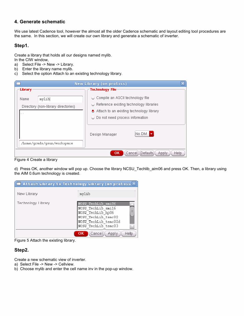
Step1. Create a library that holds all our designs named mylib. In the CIW window, a) Select File -> New -> Library. b) Enter the library name mylib. c) Select the option Attach to an existing technology library.
Figure 4 Create a library d) Press OK, another window will pop up. Choose the library NCSU_Techlib_aim06 and press OK. Then, a library using the AIM 0.6um technology is created.
Figure 5 Attach the existing library.
Step2. Create a new schematic view of inverter. a) Select File -> New -> Cellview. b) Choose mylib and enter the cell name inv in the pop-up window.
Figure 6 Create a new shematic Schematic editor will pop up.
Figure 7 Start the schematic editor Create instance of nmos4/pmos4 from the analogLib library.
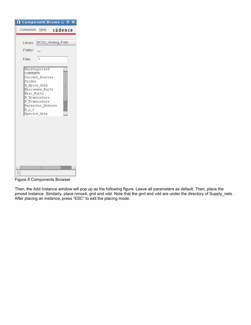
On the schematic editor, select Create -> Instance or use toolbar . Choose library NCSU_Analog_Parts in the pop-up Component Browser window. Choose pmos4 from the P_Transistors directory.
Figure 8 Components Browser Then, the Add Instance window will pop up as the following figure. Leave all parameters as default. Then, place the pmos4 instance. Similarly, place nmos4, gnd and vdd. Note that the gnd and vdd are under the directory of Supply_nets . After placing an instance, press “ESC” to exit the placing mode.
Figure 9 pmos4 instance
Figure 10 vdd instance
Create -> Pin or use toolbar . Choose appropriate direction.
Figure 11 Add pin Add wire to the source of nmos4/pmos4, pin, etc to connect them together. You can select Create -> Wire (narrow) or use
toolbar .
Check the design. Select Check -> Current Cellview to check the design. Errors will be displayed in the CIW. Correct any errors. You can find further instruction from “Help” option in CIW. There are many detailed tutorials in this option.
5. Generate netlist from the schematic and simulate it with HSPICE
Step1. Open the schematic view of inverter.
Step2. Select Launch -> ADE L, the Analog Design Environment window pop up.
Figure 12 ADE Window
Step3. Select Setup->Model libraries, add two models “ami06N” and “ami06P” from ncsu/models/hspice/public/publicModel/
Figure 13 Add models
Step4. Select Simulation->Netlist->Create to generate the following netlist:
Figure 14 Generated netlist window
Step5. Without any changes, Save the file as inv.s using the File -> Save As menu. Now you must create inv.hsp file with the following content: VDD 5.0 CLK 5.0 RISE 0.1 FALL 0.1 in 01010 ..cload out 0 20fF You may use any text editor of your choice. Save the file. Then type “hsp50 inv” to create “inv.sp” file. Both “inv.s” file and “inv.hsp” file are combined into the “inv.sp” file.
Step6. Now hspice simulate your schematic netlist using the following command: % hspice inv.sp Be sure to read the hspice output, it must say it completed and not aborted. The tpd value in the result is the propagation delay of the inverter. Once the hspice is successfully completed, you can see the input and output waveform. Type the following command: % sc inv.tr0 &
Choose the inv.tr0 from the Output View window of the SpiceCheck (sc) window and expand it. Then select “in” and “out” signals, drag them to the Waveview window. You may explore other features of the SpiceCheck program to measure the signal statistics.
6. Generate layout In this section, we will draw the layout view of the inverter. A layout describes the masks from which your design will be fabricated. The layers in a layout describe the physical characteristics of the device and have more details than a schematic. Therefore, layout verification of your design is critical. There are two types of layout design: Full-Custom and Automated. Full-custom layout is when the user physically draws all of the layers for the individual transistor. This is a very tedious process, but it usually enables results in a compacter design than the automated process. The automated process, on the other hand, is done by instantiating standard cells (reusing basic blocks) and usually takes more area but it is much faster. We only introduce custom layout design here. You should follow MOSIS SCMOS design rule for AIM 0.6µm: http://www.mosis.com/Technical/Designrules/scmos/scmos-main.html The inverter consists of three parts -- p-transistor, n-transistor, and connections.
6.1 Generate layout with macro in the library
Step1. Create a layout view for the inverter. a) Select File -> New -> Cellview. b) Choose mylib, select the cell name inv, and select layout view.
Figure 15 Create layout view c) Click OK. LSW and Layout Editor windows will pop up as shown below.
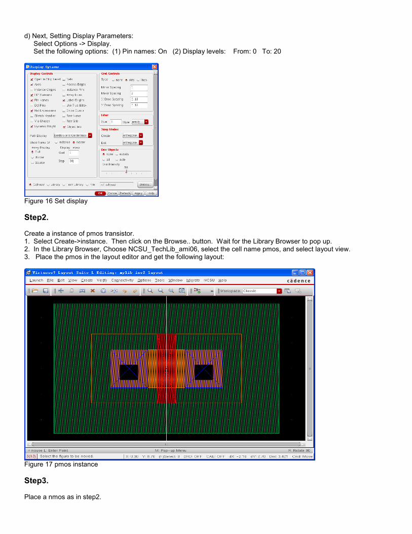
d) Next, Setting Display Parameters: Select Options -> Display. Set the following options: (1) Pin names: On (2) Display levels: From: 0 To: 20
Figure 16 Set display
Step2. Create a instance of pmos transistor. 1. Select Create->instance. Then click on the Browse.. button. Wait for the Library Browser to pop up. 2. In the Library Browser, Choose NCSU_TechLib_ami06, select the cell name pmos, and select layout view. 3. Place the pmos in the layout editor and get the following layout:
Figure 17 pmos instance
Step3. Place a nmos as in step2.
Step4. Draw the gnd next to the Nmos 1. Select the pselect layer from the LSW window; we will draw the pselect enclosing the substrate (connected to the gnd) contact for the N transistor 2. Select the Create->Rectangle 3. Draw the pselect on the cellview; it will have to enclose the contact p-active by at least 0.6.The pselect abuts directly to the nselect of the N transistor, but they should not overlap. 4. Select the pactive layer from the LSW window 5. Draw the pactive island on the cellview to be 1.2 wide by 1.5 tall; it must be enclosed by the pselect by 0.6. 6. Add contacts in the center of the substrate-contact island.
Step5. Draw the Vdd next to the nmos as in the previous step.
Step6.
1. Connect the source of p-transistor to the well-contact using the metal 1 layer. 2. Connect the source of n-transistor to the substrate-contact with the metal 1. 3. Add a contact to the gate (poly)
Figure 18 Layout of inverter
6.2 Generate layout layer by layer
Step1. Same as step1 in 4.1
Step2. Layout of P-transistor with L=0.6µm and W=1.5 µm. Since we are using the Nwell process technology, the substrate will be p-substrate. We will create a pmos transistor first. To do that we need an Nwell in which the pmos transistor will be formed.
a) Draw the well
1.Select the n-well layer from the LSW window
2. Select the Create->Rectangle (or use hotkey R). 3. Draw the n-well on the cellview to be 7.2 wide by 7.2 tall. b) Draw the p- select regions for the p transistor 1. Select the pselect layer from the LSW window; we will draw the pselect enclosing the transistor 2. Select the Create->Rectangle. 3. Draw the pselect on the cellview; 4.8 wide and 2.7 tall; its Left- and Right-edges should be 0.6 away from well edges. The pselect should be placed within the n-well, even if the size should vary (you can use the Edit->move or hotkey m command to move the layer) . c) Draw Diffusions 1. Select the pactive layer from the LSW window; draw the active region of the p-device with size 1.5 X 3.6 2. Add a contact in the center of the well-contact island with the size 0.6 X 0.6 d) Similarly, draw the nmos transistor and connect them. e) Draw the substrate-contact as in step 4 of 4.1. f) Draw metal Connections as in step 6 of 4.1 and get the same layout as in figure 14.
Step3. Draw the vdd and gnd as in section 5.1.
6.3 DRC rule check. DRC is used to check that all process-specific design rules (such as spacing) have been met. There are process-specific design rules that describe how close layers can be placed together and what the sizes of the areas can be. These rules are giving the minimum requirement to avoid a catastrophic failure of your circuit due to fabrication faults. You can use the following MOSIS SCMOS design rules as a guideline. The design rules are different for different processes. In the layout editor, select Verify-> DRC
Figure 19 DRC If your design has violated any design rules, DRC will reports the errors in the CIW. Errors are indicated by the markers (white color) on the circuit. You may then proceed to correcting the errors according to the design rules. For huge layouts, the marker might not be easily located. To find markers, choose Verify -> Markers -> Find in layout window. A pop-up menu will appear. Select on the Zoom to Markers box. Click on the Apply button and Cadence will zoom in to the errors or warnings as desired.
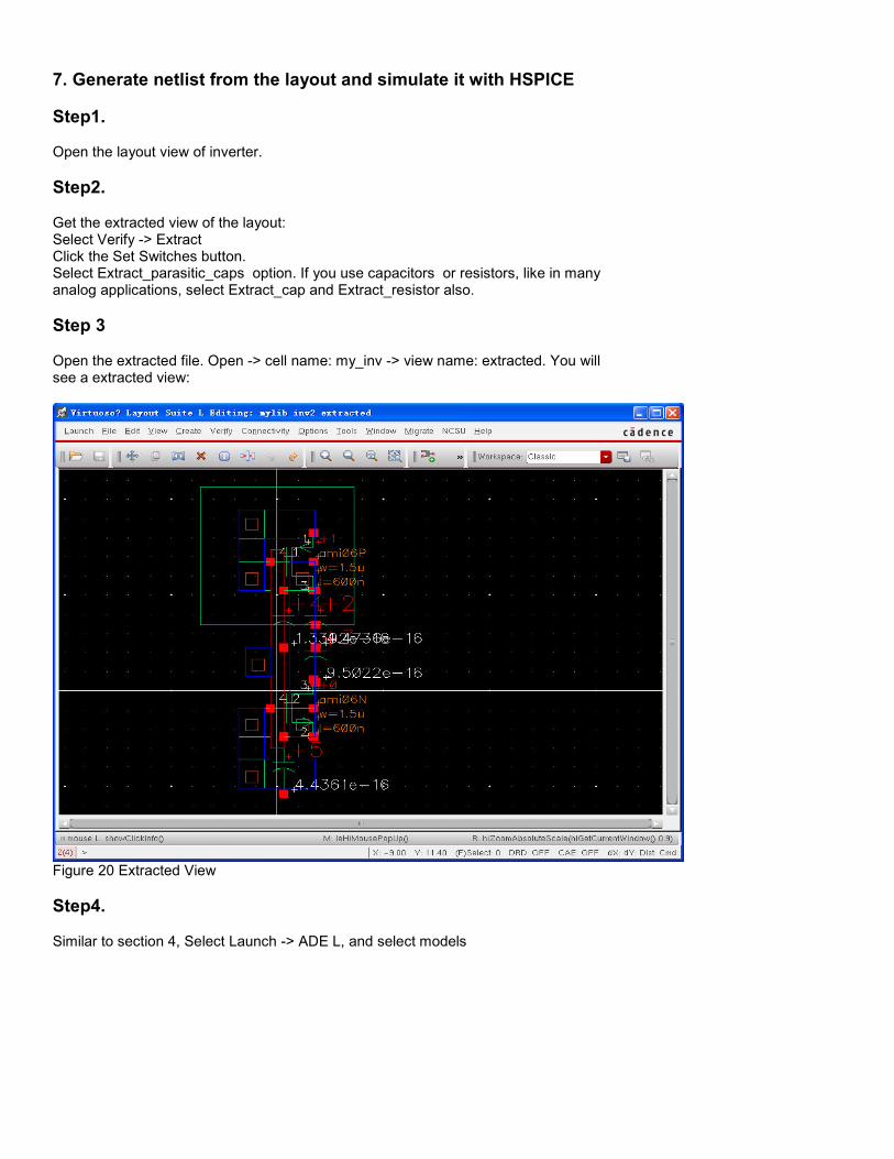
7. Generate netlist from the layout and simulate it with HSPICE
Step1. Open the layout view of inverter.
Step2. Get the extracted view of the layout: Select Verify -> Extract Click the Set Switches button. Select Extract_parasitic_caps option. If you use capacitors or resistors, like in many analog applications, select Extract_cap and Extract_resistor also.
Step 3 Open the extracted file. Open -> cell name: my_inv -> view name: extracted. You will see a extracted view:
Figure 20 Extracted View
Step4. Similar to section 4, Select Launch -> ADE L, and select models
Figure 21 ADE Window Select Setup->Model libraries, add two models “amio6N” and “ami06P” from ncsu/models/hspice/public/publicModel/
Figure 22 Add models
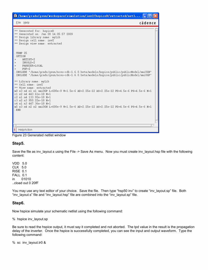
Step5. Select Simulation->Netlist->Create to generate the following netlist. Compare with that in section 4.
Figure 23 Generated netlist window
Step5. Save the file as inv_layout.s using the File -> Save As menu. Now you must create inv_layout.hsp file with the following content: VDD 5.0 CLK 5.0 RISE 0.1 FALL 0.1 in 01010 ..cload out 0 20fF You may use any text editor of your choice. Save the file. Then type “hsp50 inv” to create “inv_layout.sp” file. Both “inv_layout.s” file and “inv_layout.hsp” file are combined into the “inv_layout.sp” file.
Step6. Now hspice simulate your schematic netlist using the following command: % hspice inv_layout.sp Be sure to read the hspice output, it must say it completed and not aborted. The tpd value in the result is the propagation delay of the inverter. Once the hspice is successfully completed, you can see the input and output waveform. Type the following command: % sc inv_layout.tr0 &
Choose the inv_layout.tr0 from the Output View window of the SpiceCheck (sc) window and expand it. Then select “in” and “out” signals, drag them to the Waveview window. You may explore other features of the SpiceCheck program to measure the signal statistics. The tpd value in the result is the propagation delay of the inverter. Compare with the result from section 4.
8. Create symbol view and generate layout from the symbol
Step1. Create the symbol from the schematic
Open the schematic view of inverter, and choose “Create->Cellview->From Cellview”
Keep the default set up and create the symbol view of inverter.
Step2. Generate layout from the symbol Create a new schematic view and add create two instances of inverters symbols.
In the schematic view window, select Launch->Layout XL. We will see the XL Editor and two layout instances in the right
window. Note that you should connect the two layout of inverters with Metal2 layer manually (the automatic layout
generator doesn’t create wire connections).
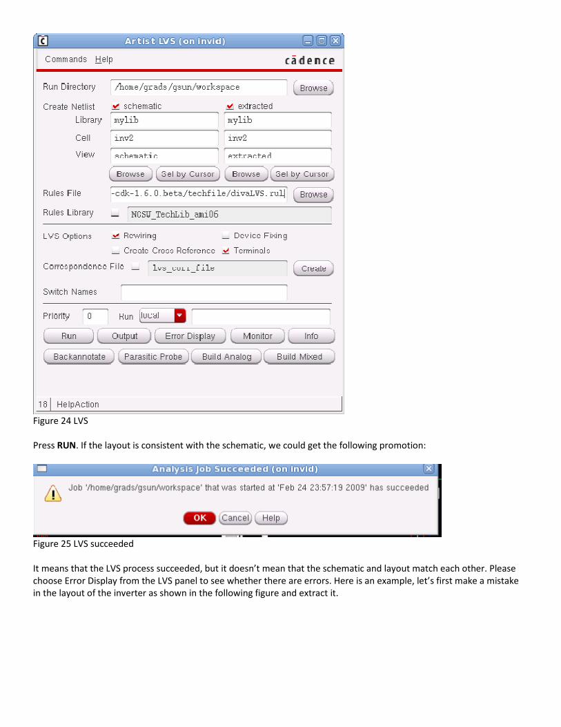
9. LVS The LVS rule check is to verify the consistence between the layout and the schematic. The layout should verified before
the further simulation.
Since now we have already got the schematic and extracted views of inverter. We could do the LVS check with the
extracted view. Open the extracted view and choose Verify->LVS, the following window will pop up. De-select the rule
library and input the LVS Rule file “/home/faculty/kyusun/c411/ncsu-cdk-1.6.0.beta/techfile/divaLVS.rul”:
Figure 24 LVS
Press RUN. If the layout is consistent with the schematic, we could get the following promotion:
Figure 25 LVS succeeded
It means that the LVS process succeeded, but it doesn’t mean that the schematic and layout match each other. Please
choose Error Display from the LVS panel to see whether there are errors. Here is an example, let’s first make a mistake
in the layout of the inverter as shown in the following figure and extract it.
Figure 26 Layout mismatch
After doing the LVS and check errors, we could get six errors (actually they are all caused by the disconnection
mismatch), shown as in the following figures. You could zoom to the problem place and find that the problem is
highlighted (pink part). Then, you can fix the problem.