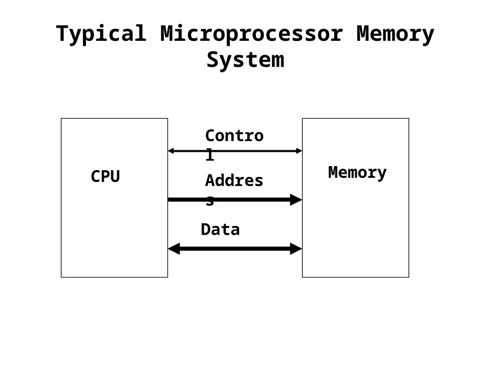
CPU Main Memory Five Components of a Computer Output Device s Input Device s Secondary Memory display screen, printer keyboard, mouse harddisks, floppy disks, tapes, CD-ROMs CPU - Central Processing Unit fetches and follows a set of simple instructions Main Memory stores the executing program and its data in RAM ( random access memory ) Secondary Memory stores permanent records ( files )
Transcript
CPU
MainMemory
Five Components of a Computer
OutputDevices
InputDevices
SecondaryMemory
display screen,printer
keyboard,mouse
harddisks, floppy disks,tapes, CD-ROMs
CPU - Central Processing Unit fetches and follows a set of simple instructions
Main Memory stores the executing program and its data in RAM ( random access memory )
Secondary Memory stores permanent records ( files )
Two Principal Microcomputer System Components
• Hardware• Software
Microprocessor(CPU)
I/O SystemMemorySystem
BUS BUS
Random Access Memory (RAM)Dynamic, StaticCache, Flash MemoryRead Only Memory (ROM)
Hardware: Architecture of a computer - general layout of major Components
System Block Diagram
System bus (data, address & control signals)
Memory
Interrupt circuitrySerial I/OParallel I/O
Timing CPU
P + associated logic circuitry:
•Bus controller
•Bus drivers
•Coprocessor
•ROM (Read Only Memory) (start-up program)•RAM (Random Access Memory)•DRAM (Dynamic RAM) - high capacity, refresh needed•SRAM (Static RAM) - low power, fast, easy to interface
•Crystal oscillator•Timing circuitry(counters dividing to lower frequencies)
At external unexpected events, P has to interrupt the main program execution, service the interrupt request (obviously a short subroutine) and retake the main program from the point where it was interrupt.
Simple (only two wires + ground) but slow.•Printer (low resolution)•Modem•Operator’s console•Mainframe•Personal computer
Many wires, fast.•Printer (high resolution)•External memory
•Floppy Disk •Hard Disk•Compact Disk
•Other high speed devices
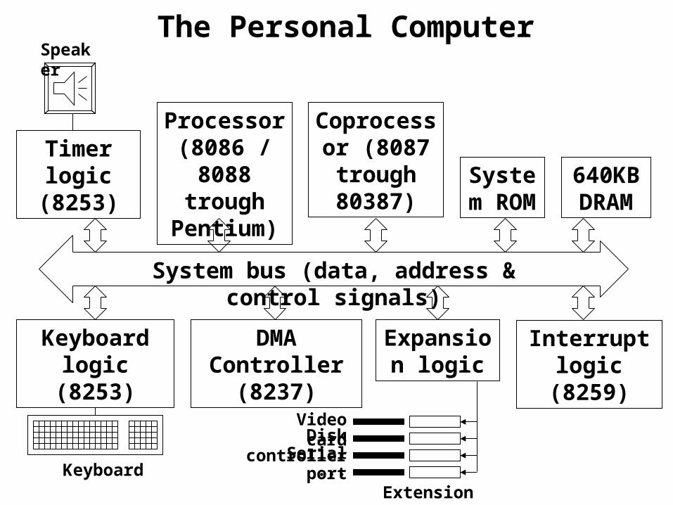
The Personal Computer
Processor (8086 / 8088
trough Pentium)
System bus (data, address & control signals)
System ROM
Interrupt logic (8259)
Keyboard logic (8253)
DMA Controller
(8237)
Timer logic
(8253)
Coprocessor (8087
trough 80387)
640KB DRAM
Expansion logic
Keyboard
Speaker
Extension slots
Video cardDisk controller
Serial port...
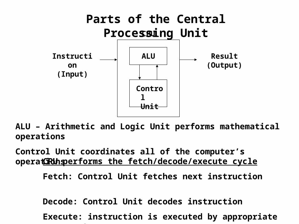
CPU performs the fetch/decode/execute cycle
Fetch: Control Unit fetches next instruction
Decode: Control Unit decodes instruction
Execute: instruction is executed by appropriate component
ALU
Control Unit
Parts of the Central Processing Unit
Instruction(Input)
ALU – Arithmetic and Logic Unit performs mathematical operations
Control Unit coordinates all of the computer’s operations
Result(Output)
CPU
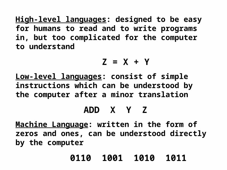
High-level languages: designed to be easy for humans to read and to write programs in, but too complicated for the computer to understand
Z = X + Y
Low-level languages: consist of simple instructions which can be understood by the computer after a minor translation
ADD X Y Z
Machine Language: written in the form of zeros and ones, can be understood directly by the computer
0110 1001 1010 1011
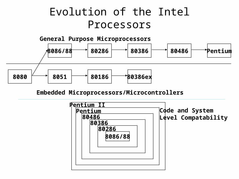
Evolution of Microprocessors
Computers “generations”• First generation ENIAC (vacuum tubes)• Second generation (transistors)• Third generation (IC - SSI, MSI)• Fourth generation (LSI)• Fifth generation can think?
MicroprocessorsMSI Intel® 4004™, 8008™LSI Intel® 8080™, Zilog® Z80™, Motorola® 6800™• 8 bit data bus, 16 bit address bus (64kbyte=65536 byte of• addressable memory), no multiply and divide instructions •
VLSI 32…64 bit data bus, 2-300MHz clock, RISC concept
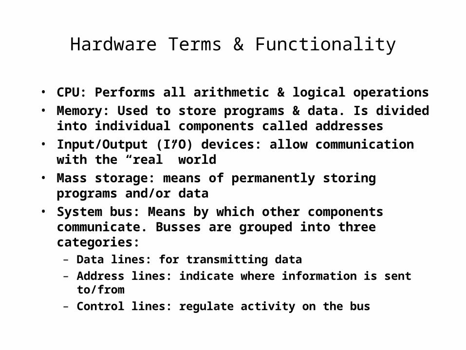
Hardware Terms & Functionality
• CPU: Performs all arithmetic & logical operations• Memory: Used to store programs & data. Is divided into
individual components called addresses• Input/Output (I/O) devices: allow communication with the
“real” world• Mass storage: means of permanently storing programs
and/or data• System bus: Means by which other components
communicate. Busses are grouped into three categories:– Data lines: for transmitting data
– Address lines: indicate where information is sent to/from
– Control lines: regulate activity on the bus
In more detail, the architecture may look like the following:
CPUBus
Control
Timing
MemoryModule
MemoryModule
I/OModule
I/OModule
MassStorage
Keyboard
Interfaces frequently implemented in a microcomputer system.
DataCommunication
Control
MassStorageControl
BusSupport
ROMStaticRAM
MemoryControl
DisplayControl
KeyboardControl
Hard CopyControl
OtherDevice
DynamicRAM
PrinterKeyboardDisplay
To
Pro
cess
or
To
Mas
s S
tora
ge
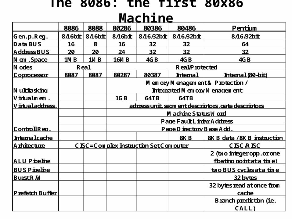
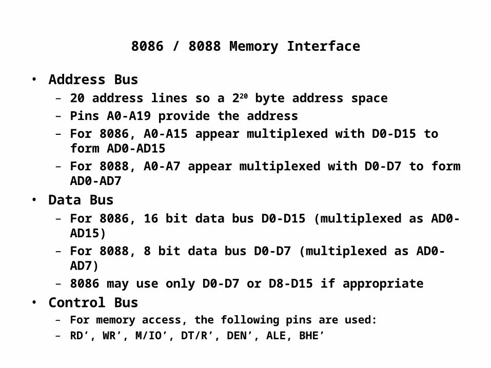
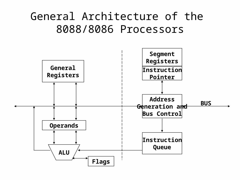
The 8086: the first 80x86 Machine8086 8088 80286 80386 80486 Pentium
Gen. p. Reg. 8/16bit 8/16bit 8/16bit 8/16/32bit 8/16/32bit 8/16/32bitData BUS 16 8 16 32 32 64Address BUS 20 20 24 32 32 32Mem. Space 1MB 1MB 16MB 4GB 4GB 4GBModesCoprocessor 8087 8087 80287 80387 Internal Internal (80-bit)
For compatibility, all the 80x86 family members start running in “Real Mode”, emulating the 8086 features (i.e. 1MB RAM)
Beginning with 80286, the “Protected Mode” is also available, allowing direct control of all address lines (all addressable memory), multitasking support, virtual memory addressing, memory management and protection (against violation from other task), control over internal data and instruction cache.
Addresses
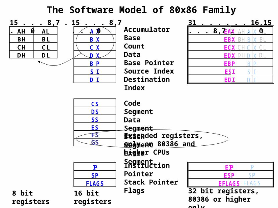
• Memory locations are comprised of groups of bits.– 8 bits: 1 byte– 16 bits: 1 word– 32 bits: 1 double word– 64 bits: 1 quad word
• Each byte has an associated address. Addresses are comprised of groups of bits.
• The set of all possible address bit combinations is called the ADDRESS SPACE.
Segment = a 64kbyte memory block beginning at a multiple by 10H address. An effective address is generated as combination between a segment register and another register as in the example.
Each segment register has a default usage (class of instructions where apply).
Multiply, divide, accessing I/O...
Counter in loop operationsMultiply, divide, pointer to I/O...
Source index in string operations...Destination index in string operations
Pointer in program flowPointer in StackControl and status flags
A prefix (66H) allows using 32 bit registers in the real mode:
db 66h;EAX instead AXmov ax,1140h;less significant 16 bits db 058bh;most significant 16 bits
15 . . . 8,7 . . . 0
16 bit registers
CSDSSSES
IPSP
FLAGS
FSGS
AccumulatorBaseCountDataBase PointerSource IndexDestination Index
Contains Carry out of MSB of resultIndicates if result has even parity Contains Carry out of bit 3 in ALIndicates if result equals zero Indicates if result is negativeProvides a single step capability for debuggingEnables/disables interrupts Controls pointer updating during string operationsIndicates that an overflow occurred in resultPriority level of current task (two bits)Indicates if current task is nested
Byte swapping: if a word has to be stored into an 8 bit wide memory at address adr, its low byte is stored at adr and its high byte at adr+1. If a word is read from an 8 bit memory at address adr, the low byte is loaded from adr and the high byte from adr+1.
Rule: low significance <=> low address
Instruction typesData transfer instructions
8086 instruction setIN Input byte or word from portLAHF Load AH from flagsLDS Load pointer using data segmentLEA Load effective addressLES Load pointer using extra segmentMOV Move to/from register/memoryOUT Output byte or word to portPOP Pop word off stackPOPF Pop flags off stackPUSH Push word onto stackPUSHF Push flags onto stackSAHF Store AH into flagsXCHG Exchange byte or wordXLAT Translate byte
Additional 80286 instructionsINS Input string from portOUTS Output string to portPOPA Pop all registersPUSHA Push all registers
Additional 80386 instructionsLFS Load pointer using FSLGS Load pointer using GSLSS Load pointer using SSMOVSX Move with sign extendedMOVZX Move with zero extendedPOPAD Pop all double (32 bit) registers POPD Pop double register POPFD Pop double flag register PUSHAD Push all double registers PUSHD Push double register PUSHFD Push double flag register
Additional 80486 instructionBSWAP Byte swap
Additional Pentium instructionMOV Move to/from control register
Instruction typesArithmetic instructions
8086 instruction setAAA ASCII adjust for additionAAD ASCII adjust for divisionAAM ASCII adjust for multiplyAAS ASCII adjust for subtractionADC Add byte or word plus carryADD Add byte or wordCBW Convert byte or wordCMP Compare byte or wordCWD Convert word to double-wordDAA Decimal adjust for additionDAS Decimal adjust for subtractionDEC Decrement byte or word by oneDIV Divide byte or wordIDIV Integer divide byte or wordIMUL Integer multiply byte or wordINC Increment byte or word by oneMUL Multiply byte or word (unsigned)NEG Negate byte or wordSBB Subtract byte or word and carry (borrow)SUB Subtract byte or word
Additional 80386 instructionsCDQ Convert double-word to
quad-wordCWDE Convert word to double-word
Additional 80486 instructionsCMPXCHG Compare and exchangeXADD Exchange and add
Additional Pentium instructionCMPXCHG8B Compare and
exchange 8 bytes
Instruction typesBit manipulation instructions
8086 instruction setAND Logical AND of byte or wordNOT Logical NOT of byte or wordOR Logical OR of byte or wordRCL Rotate left trough carry byte or wordRCR Rotate right trough carry byte or wordROL Rotate left byte or wordROR Rotate right byte or wordSAL Arithmetic shift left byte or wordSAR Arithmetic shift right byte or wordSHL Logical shift left byte or wordSHR Logical shift right byte or wordTEST Test byte or wordXOR Logical exclusive-OR of byte or word
Additional 80386 instructionsBSF Bit scan forwardBSR Bit scan reverseBT Bit testBTC Bit test and complementBTR Bit test and resetBTS Bit test and setSETcc Set byte on conditionSHLD Shift left double precisionSHRD Shift right double precision
Instruction typesString instructions
8086 instruction setCMPS Compare byte or word stringLODS Load byte or word stringMOVS Move byte or word stringMOVSB(MOVSW) Move byte string (word string)REP RepeatREPE (REPZ) Repeat while equal (zero)REPNE (REPNZ) Repeat while not equal (not zero)SCAS Scan byte or word stringSTOS Store byte or word string