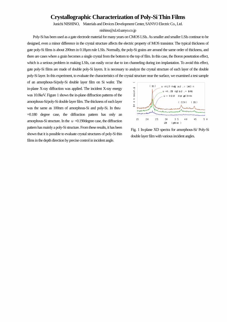
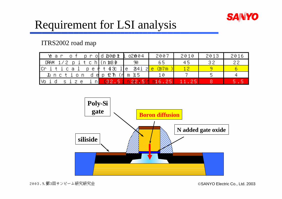
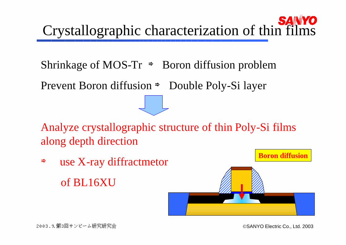
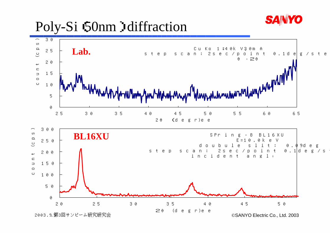
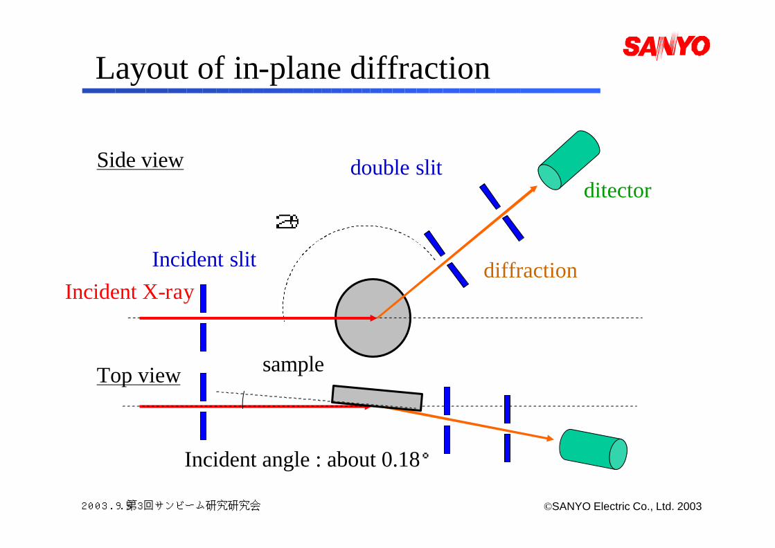
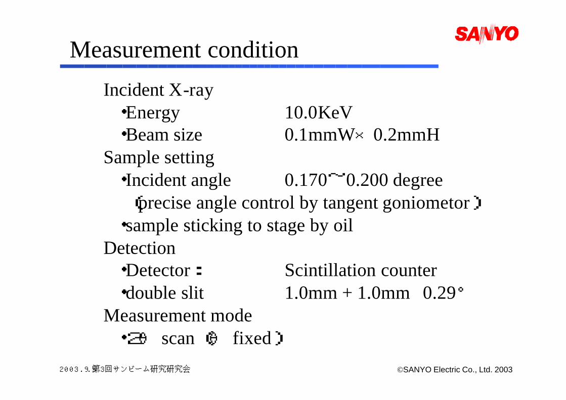
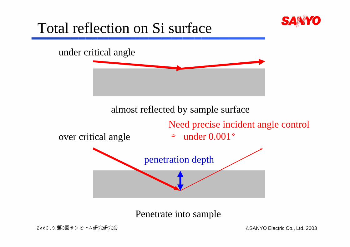
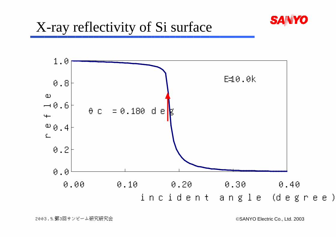
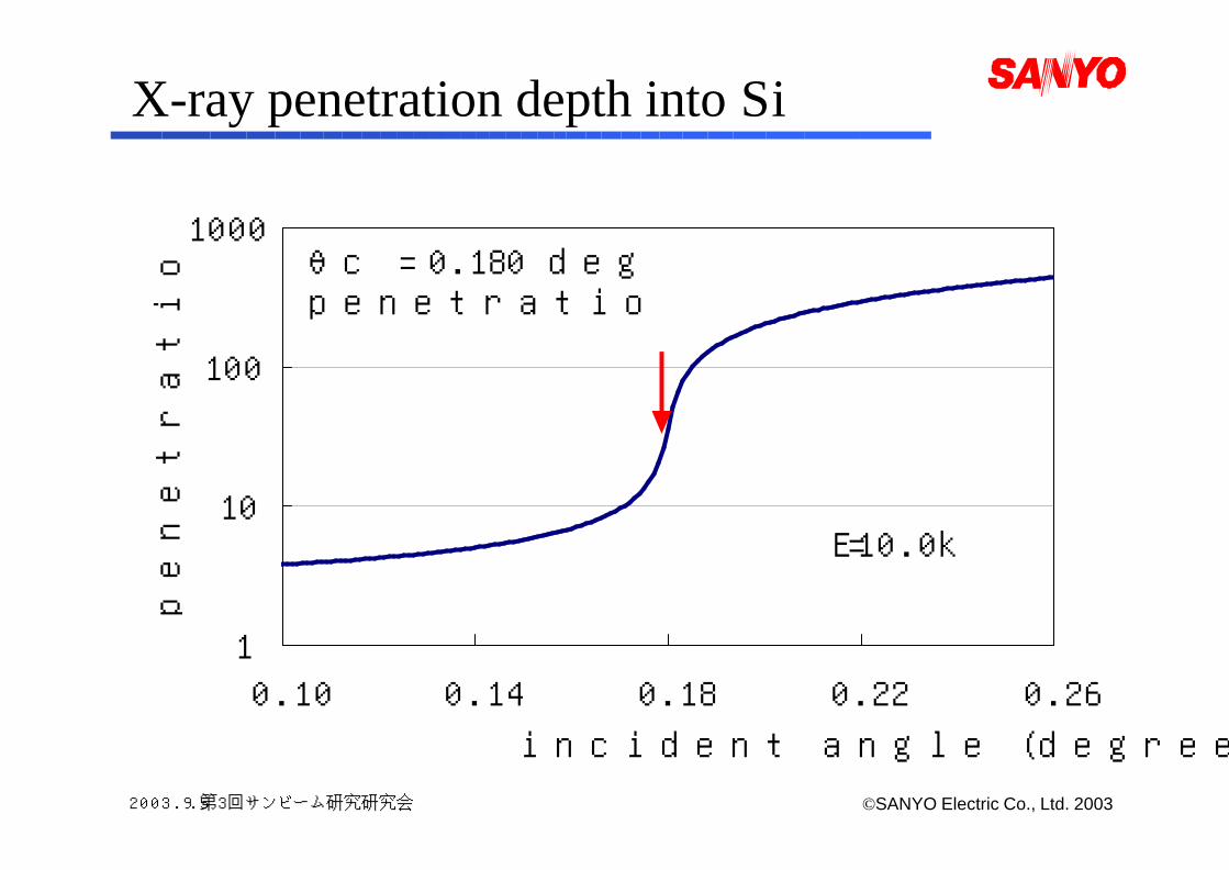
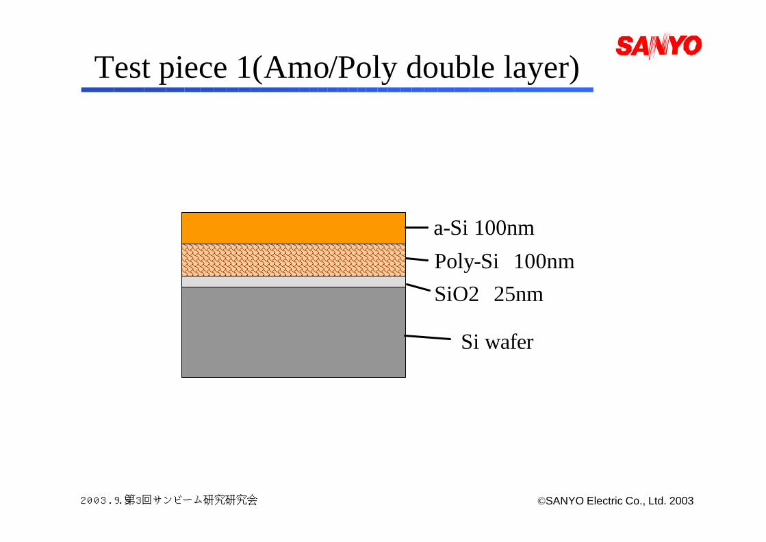
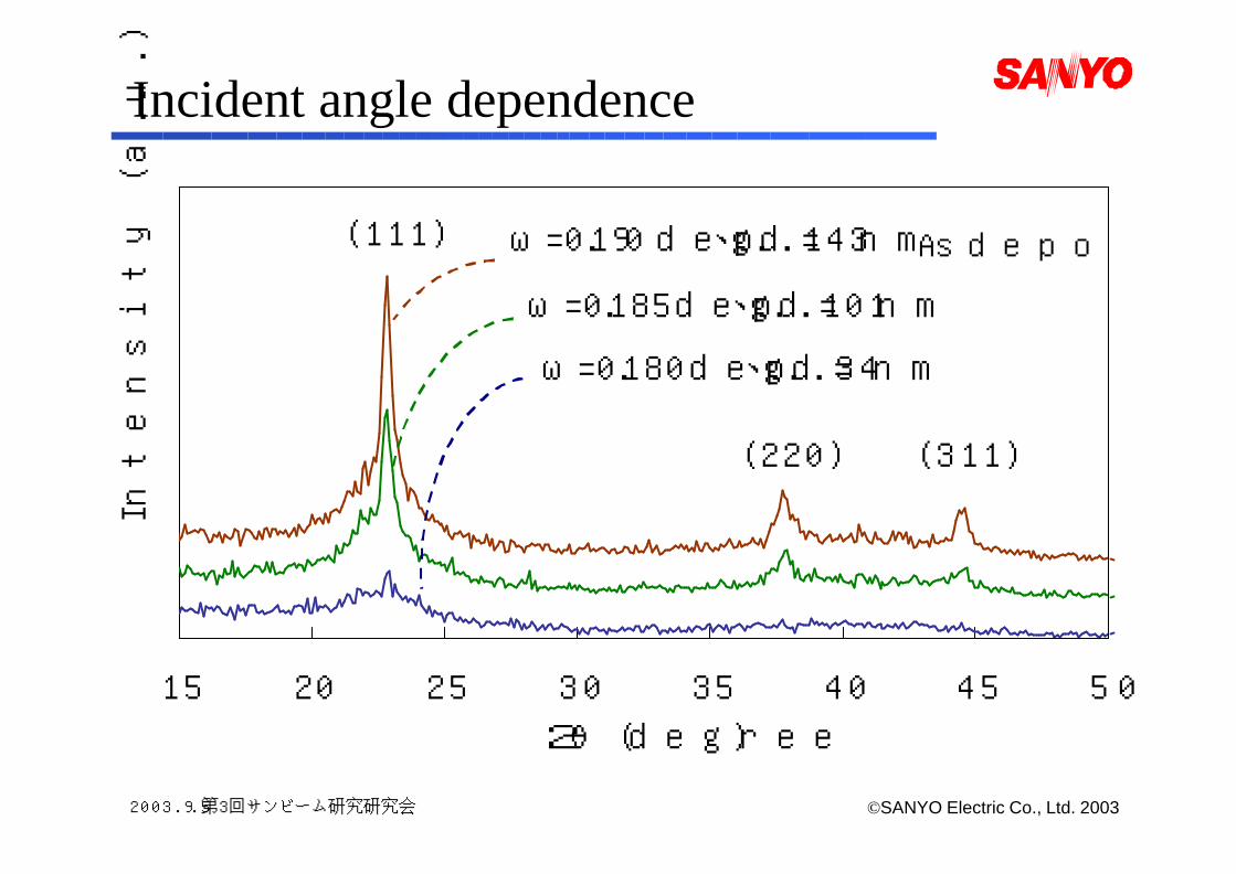
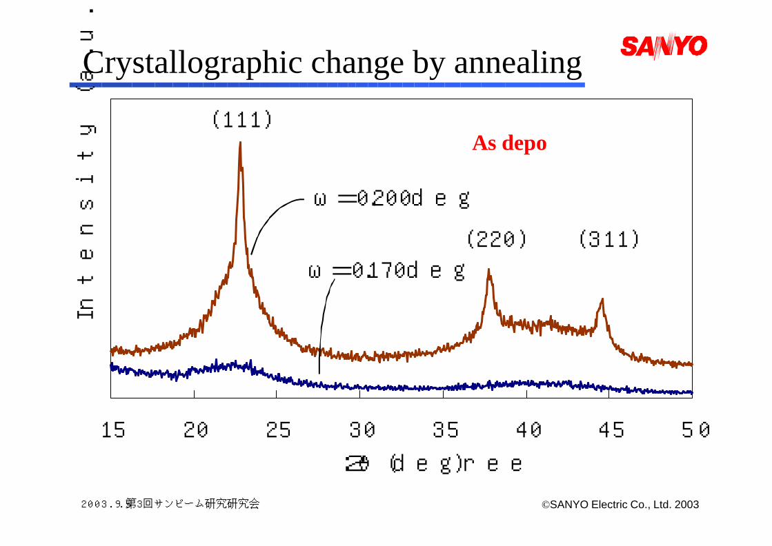
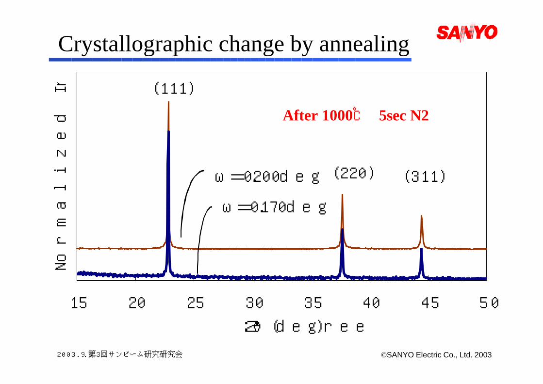
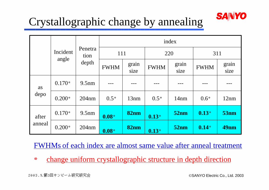
Crystallographic Characterization of Poly-Si Thin Films Junichi NISHINO, Materials and Devices Development Center, SANYO Electric Co., Ltd. [email protected]Poly-Si has been used as a gate electrode material for many years on CMOS LSIs. As smaller and smaller LSIs continue to be designed, even a minor difference in the crystal structure affects the electric property of MOS transistor. The typical thickness of gate poly-Si films is about 200nm in 0.18μm rule LSIs. Normally, the poly-Si grains are around the same order of thickness, and there are cases where a grain becomes a single crystal from the bottom to the top of film. In this case, the Boron penetration effect, which is a serious problem in making LSIs, can easily occur due to ion channeling during ion implantation. To avoid this effect, gate poly-Si films are made of double poly-Si layers. It is necessary to analyze the crystal structure of each layer of the double poly-Si layer. In this experiment, to evaluate the characteristics of the crystal structure near the surface, we examined a test sample of an amorphous-Si/poly-Si double layer film on Si wafer. The in-plane X-ray diffraction was applied. The incident X-ray energy was 10.0keV. Figure 1 shows the in-plane diffraction patterns of the amorphous-Si/poly-Si double layer film. The thickness of each layer was the same as 100nm of amorphous-Si and poly-Si. In the ω =0.180 degree case, the diffraction pattern has only an amorphous-Si structure. In the ω =0.190degree case, the diffraction pattern has mainly a poly-Si structure. From these results, it has been shown that it is possible to evaluate crystal structures of poly-Si thin films in the depth direction by precise control in incident angle. 15 20 25 30 35 40 45 50 2θ (de gree) Intensity ( a.u.) ω=0.1 80 deg 、p.d .=34 nm ω=0.18 5 d eg、p.d.=101 nm (1 11) (3 11) (220) ω=0.190 d eg、p.d.=143n m Fig. 1 In-plane XD spectra for amorphous-Si/ Poly-Si double layer film with various incident angles.
Transcript
Crystallographic Characterization of Poly-Si Thin Films
Junichi NISHINO, Materials and Devices Development Center, SANYO Electric Co., Ltd.
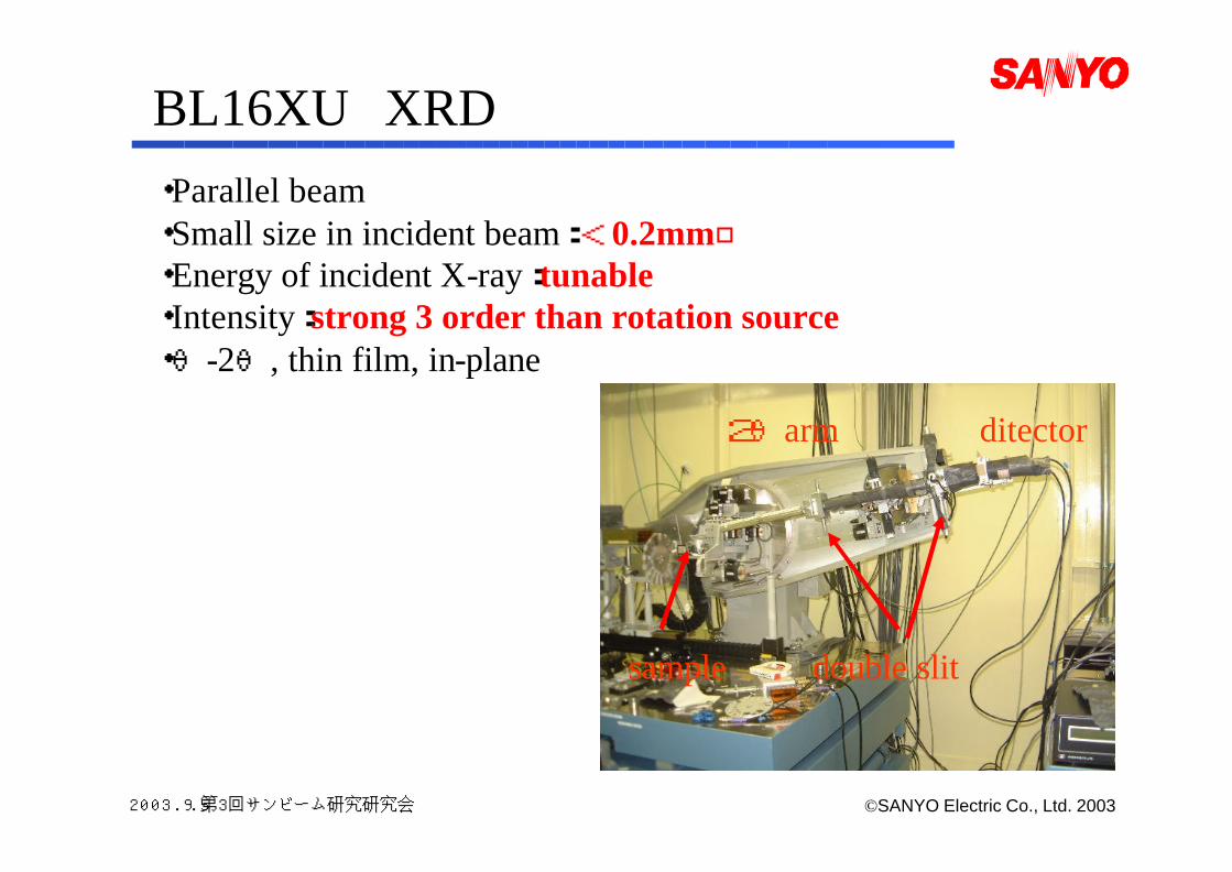
BL16XU XRD・Parallel beam・Small size in incident beam:<0.2mm□・Energy of incident X-ray:tunable・Intensity:strong 3 order than rotation source・θ-2θ, thin film, in-plane