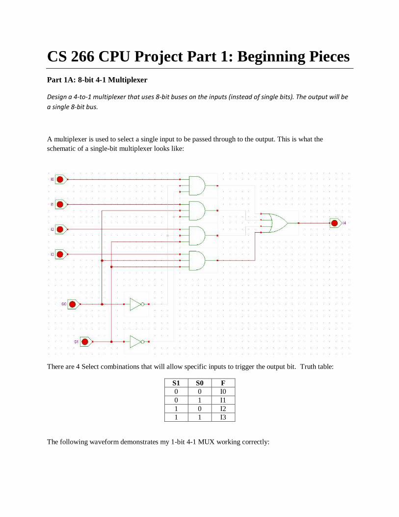
CS 266 CPU Project Part 1: Beginning Pieces Part 1A: 8-bit 4-1 Multiplexer Design a 4-to-1 multiplexer that uses 8-bit buses on the inputs (instead of single bits). The output will be a single 8-bit bus. A multiplexer is used to select a single input to be passed through to the output. This is what the schematic of a single-bit multiplexer looks like: There are 4 Select combinations that will allow specific inputs to trigger the output bit. Truth table: S1 S0 F 0 0 I0 0 1 I1 1 0 I2 1 1 I3 The following waveform demonstrates my 1-bit 4-1 MUX working correctly:
Transcript
CS 266 CPU Project Part 1: Beginning Pieces
Part 1A: 8-bit 4-1 Multiplexer
Design a 4-to-1 multiplexer that uses 8-bit buses on the inputs (instead of single bits). The output will be
a single 8-bit bus.
A multiplexer is used to select a single input to be passed through to the output. This is what the
schematic of a single-bit multiplexer looks like:
There are 4 Select combinations that will allow specific inputs to trigger the output bit. Truth table:
S1 S0 F
0 0 I0
0 1 I1
1 0 I2
1 1 I3
The following waveform demonstrates my 1-bit 4-1 MUX working correctly:
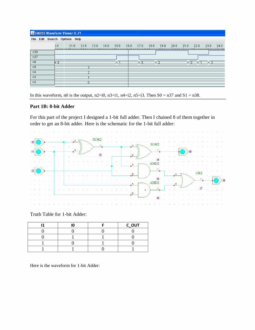
For reference, in0…3p = I0…3
n0 is the output, n7 is S0, and n3 is S1
To implement an 8bit 4-1 Multiplexer I used Expanders to attach each 8bit value to 8 4-1 Multiplexers.
Here is the schematic:
The condensed truth table remains the same:
S1 S0 F
0 0 I0
0 1 I1
1 0 I2
1 1 I3
Here is the waveform:
In this waveform, n0 is the output, n2=i0, n3=i1, n4=i2, n5=i3. Then S0 = n37 and S1 = n38.
Part 1B: 8-bit Adder
For this part of the project I designed a 1-bit full adder. Then I chained 8 of them together in
order to get an 8-bit adder. Here is the schematic for the 1-bit full adder:
Truth Table for 1-bit Adder:
I1 I0 F C_OUT
0 0 0 0
0 1 1 0
1 0 1 0
1 1 0 1
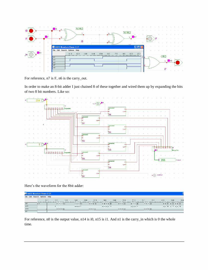
Here is the waveform for 1-bit Adder:
For reference, n7 is F, n6 is the carry_out.
In order to make an 8-bit adder I just chained 8 of these together and wired them up by expanding the bits
of two 8 bit numbers. Like so:
Here’s the waveform for the 8bit adder:
For reference, n0 is the output value, n14 is i0, n15 is i1. And n1 is the carry_in which is 0 the whole
time.
CS 266 CPU Project Part 2: The ALU
For this part of the project we were tasked to build a working 8-bit ALU with 8 operations. An ALU is an
arithmetic logic unit. It handles the mathematical operations a processor computes. Here are the
operations we were tasked with handling:
Alu_sel action
0 A OR B
1 Not(A)
2 A + not(b) + c_in
3 A + B + c_in
4 A XOR B
5 A AND B
6 A – 1 + c_in
7 A + c_in
We have broken the actions up and explained them in the order they are selected. At the end of this pdf
we will put it all together to complete the ALU.
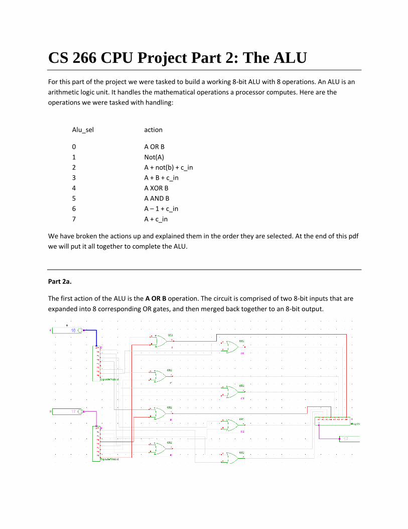
Part 2a.
The first action of the ALU is the A OR B operation. The circuit is comprised of two 8-bit inputs that are
expanded into 8 corresponding OR gates, and then merged back together to an 8-bit output.
Here is the corresponding waveform for the A OR B operation. The output is A or B.
In this waveform, n2 is B, n1 is A, and n26 is the output.
Part 2b
The next circuit diagram is for the notA component of the ALU. When alu_sel = 1 this circuit is utilized to
flip the bits of the input. It was constructed by expanding an 8bit input and running lines through 8
inverters. Then those inverted bits flow into an 8bit merger to produce the output of notA.
The following waveforms prove that the above circuit works correctly. Each input is flipped. Since it was
tested in Decimal you must subtract the input from 255 and you get the “flipped” output.
Waveform for the notA component.
Part 2c
The third operation to be implemented by our ALU is the A + not(B) + c_in operation. We accomplished
this by taking our 8-bit full adder and placing an 8bit Inverter (seen above) in between inputB and it’s
expander bit. This gets us the not(B) we are looking for.
In this waveform n0 is output, n1 is c_in, n15 is B, and n14 is A.
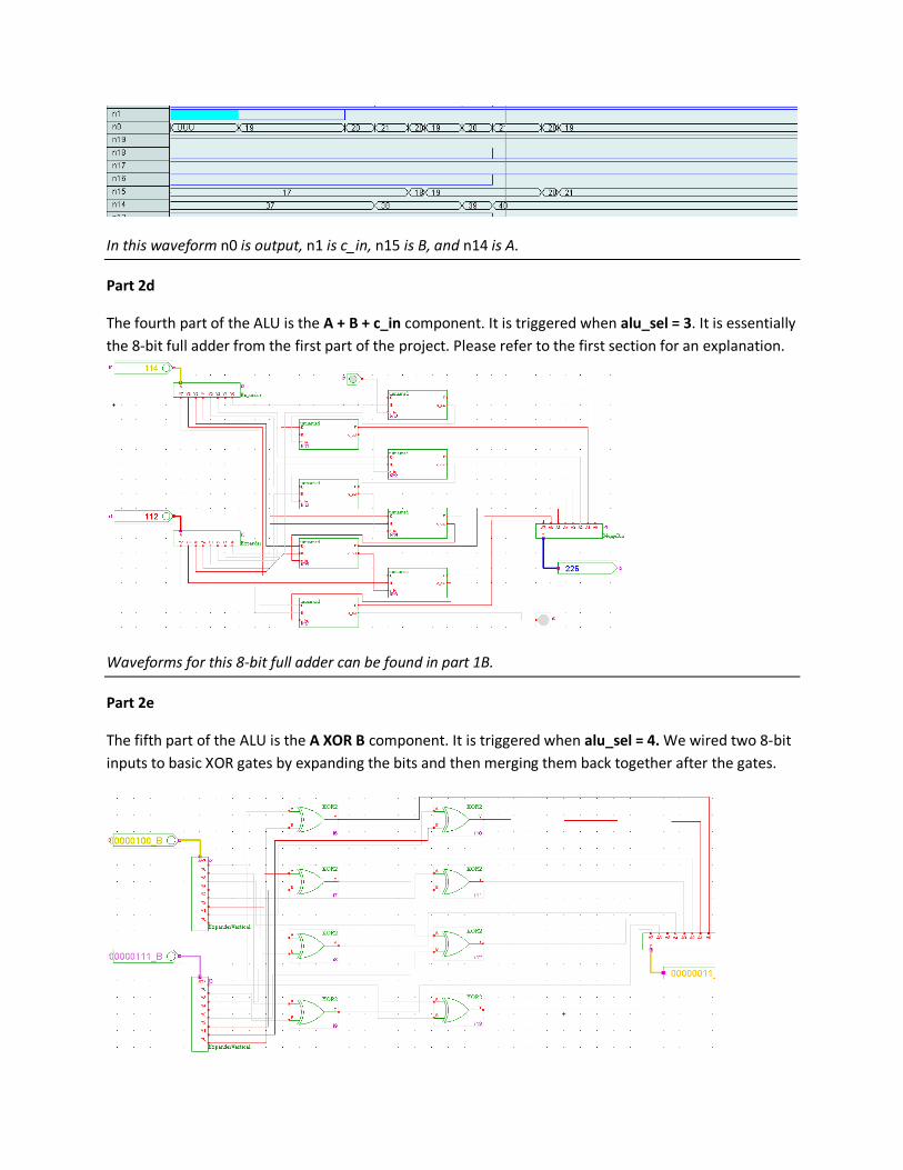
Part 2d
The fourth part of the ALU is the A + B + c_in component. It is triggered when alu_sel = 3. It is essentially
the 8-bit full adder from the first part of the project. Please refer to the first section for an explanation.
Waveforms for this 8-bit full adder can be found in part 1B.
Part 2e
The fifth part of the ALU is the A XOR B component. It is triggered when alu_sel = 4. We wired two 8-bit
inputs to basic XOR gates by expanding the bits and then merging them back together after the gates.
Any bit that differs from the two inputs is represented in the output. If both inputs have a 1 or a 0 in the
same bit placing then a 0 is reflected in the output:
In this waveform, n1 is B, n0 is A, and n26 is the output A XOR B.
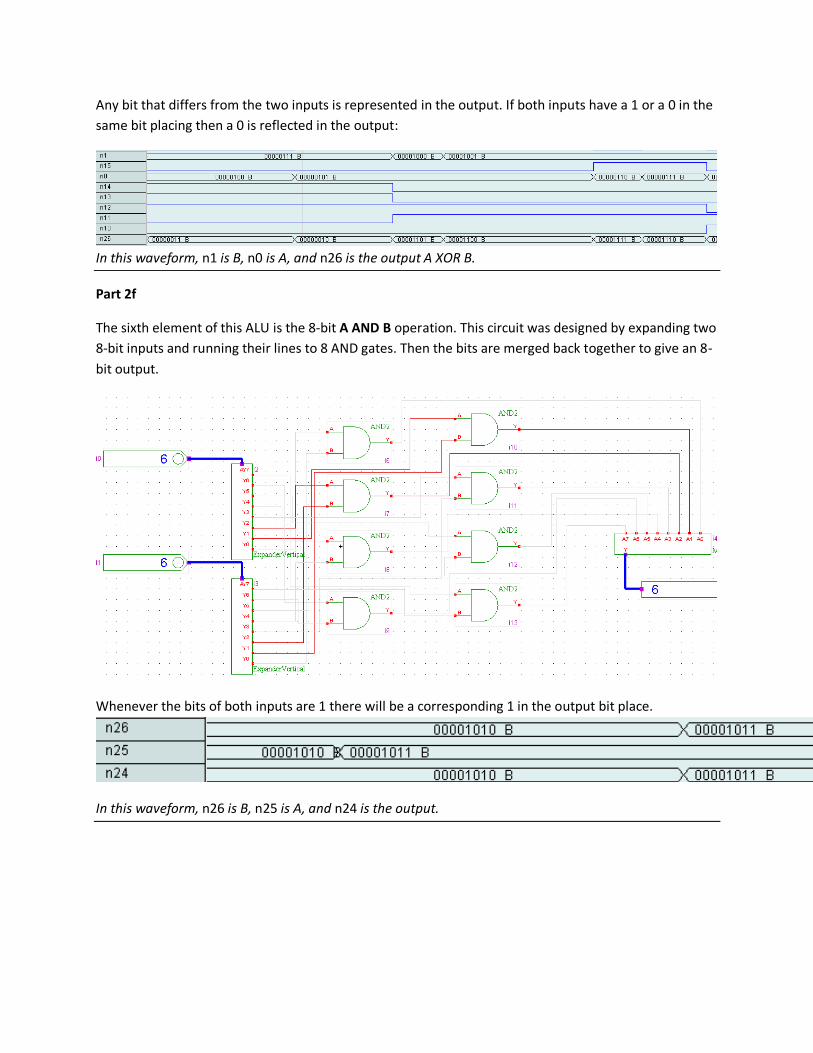
Part 2f
The sixth element of this ALU is the 8-bit A AND B operation. This circuit was designed by expanding two
8-bit inputs and running their lines to 8 AND gates. Then the bits are merged back together to give an 8-
bit output.
Whenever the bits of both inputs are 1 there will be a corresponding 1 in the output bit place.
In this waveform, n26 is B, n25 is A, and n24 is the output.
Part 2g
The seventh component of the ALU is the A – 1 + c_in operation. This takes the value of A and subtracts
one from it. In order to construct this circuit we wired Vcc to the second input of a 7-bit adder and set
the most significant bit of the output to be zero. When the input is 127 or lower, it is subtracted by one.
When the input is greater than 127, it is turned into 2’s complement and the 2’s complement led is
triggered. C_in is also added to the input.
In this waveform, n0 is the output, n14 is the input, and n0 is the c_in.
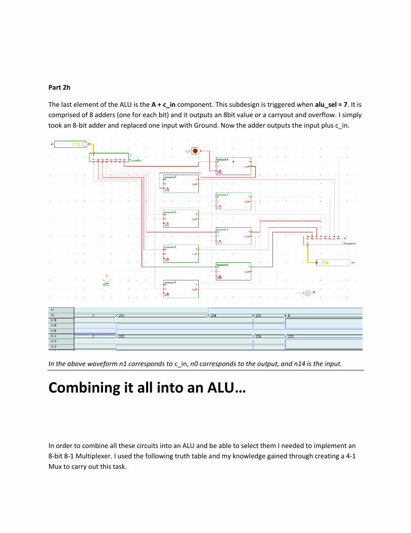
Part 2h
The last element of the ALU is the A + c_in component. This subdesign is triggered when alu_sel = 7. It is
comprised of 8 adders (one for each bit) and it outputs an 8bit value or a carryout and overflow. I simply
took an 8-bit adder and replaced one input with Ground. Now the adder outputs the input plus c_in.
In the above waveform n1 corresponds to c_in, n0 corresponds to the output, and n14 is the input.
Combining it all into an ALU…
In order to combine all these circuits into an ALU and be able to select them I needed to implement an
8-bit 8-1 Multiplexer. I used the following truth table and my knowledge gained through creating a 4-1
Mux to carry out this task.
S2 S1 S0 F
0 0 0 I0
0 0 1 I1
0 1 0 I2
0 1 1 I3
1 0 0 I4
1 0 1 I5
1 1 0 I6
1 1 1 I7
Then I expanded eight 8-bit numbers into eight subdesigns of this 8-1 MUX:
The ALU
Here it is, in all its glory, the almighty ALU:
In this waveform n0 is A, n1 is B, and n7 is ALU_SELECT.
n8 is AorB, n9 is notA, n10 is A+not(b)+c_in, n11 is A+B+c_in, n12 is aXORb, n13 is AandB, n14 is
A-1+c_in, and n15 is A+c_in.
References: Mano and Kime. Logic and Computer Design Fundamentals. 2008