51
CSE241A L12 Verification 1 A. B. Kahng, UCSD 2003 CSE241 VLSI Digital Circuits Winter 2003 Lecture 13: Verification
| Date post: | 22-Apr-2018 |
| Category: |
Documents |
| Upload: | doannguyet |
| View: | 217 times |
| Download: | 0 times |

CSE241A L12 Verification 1 A. B. Kahng, UCSD 2003
CSE241VLSI Digital Circuits
Winter 2003
Lecture 13: Verification

CSE241A L12 Verification 2 A. B. Kahng, UCSD 2003
Takehome Midterm QuestionsDirections: Open-book/notes. Spend at most 4 hours, including writing up using at most 5 pages. Turn in a neat hardcopy at the end of Lecture 15. Also turn in Ben’s midterm questions at that time, if you haven’t already done so.
Question 1: Clocking and Place-Route Flow. Consider the following steps:Clock sink placementStandard-cell global placementStandard-cell detailed placementStandard-cell ECO placementClock buffer tree constructionGlobal signal routingDetailed signal routingBounded-skew (balanced) clock (sub)net routingSteiner clock (sub)net routingClock sink useful skew scheduling (i.e., solving the linear program, etc.)Post-placement (global routing based) static timing analysisPost-detailed routing static timing analysis
(A) As the designer of a clock distribution flow for high-performance standard-cell based ASICs, how would you use and order these steps? It is possible to use some steps more than once, others not at all (e.g., if subsumed by other steps). (B) List the criteria you used for assessing possible flows. (C) What were the 3 next-best flows that you considered (describe as variants of your flow), and explain why you prefer your given answer. (10 points)

CSE241A L12 Verification 3 A. B. Kahng, UCSD 2003
Takehome Midterm QuestionsQuestion 2: Scaling of Dynamic Clock Power. As we move from one technology node to the next, suppose that:
Minimum feature size (Lgate) is scaled by 0.7xAll metal layers (width, pitch) scale with minimum feature size except for Mtop which is unscaledSupply voltage is scaled by 0.85xClock frequency is scaled by 2xWire thickness remains the same for Mtop, Mx, and M1, but the number of metal layers increases by 1The number of clock sinks in a given-size (say, 1cm2) die doublesThe maximum number of loads driven by any given buffer in the clock buffer tree remains constant at 4, and somehow all buffers are the same multiple (e.g., PMOS W/L = 80) of minimum-size The clock is distributed by a perfectly balanced, buffered H-tree (so, sinks are placed on a perfect grid, etc.)
Give your analysis of how dynamic power dissipation due to clock distribution scales every TWO technology nodes, for a constant-size die. Note any additional assumptions needed. You can break up your analysis into different components (wire capacitance, gate capacitance, etc.) as you find appropriate. (10 points)
Question 3: Design Data Volume. If we migrate to the next technology node and double the gate count of a design, how would you expect the size of the LEF and routed DEF files to change? Explain your reasoning. (5 points)

CSE241A L12 Verification 4 A. B. Kahng, UCSD 2003
Homework SolutionsQ4. Coupling can be controlled by:
- Introduction of shield lines that are tied to power or ground supplies; these give stable MCF = 1 to nearest-neighbors (no delay uncertainty due to capacitive coupling) and also closer current return paths (less loop area less inductance). Dedicated ground and power planes are also possible.
- Increased spacing between lines (reduces capacitive coupling).- Control of slew times to be between prescribed lower and upper bounds; too-short
slew times create strong aggressor lines, while too-long slew times create weak victim lines.
- Sizing of gates to juggle drive strengths and load capacitances, in order to control slew times.
- Staggering of repeaters so that worst-case MCF can occur only along one half of the repeater distance (= period between consecutive repeaters), and if it does, best-case MCF will occur along the other half.
- Swizzling, e.g., of parallel bus wires can prevent long parallel runs of neighboring interconnects; sometimes this is effectively achieved by “randomization” of the routing (a feature, not a bug).
- Inductance can also cause L di/dt supply noise, and this can be controlled by power/ground network design, location and assignment of power/ground pins, explicitly added decoupling capacitances, and increasing slew times.
CSE241A L12 Verification 5 A. B. Kahng, UCSD 2003
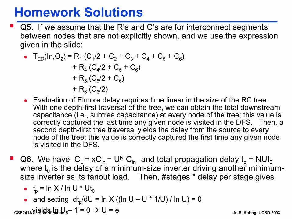
Homework SolutionsQ5. If we assume that the R’s and C’s are for interconnect segments between nodes that are not explicitly shown, and we use the expression given in the slide:
TED(In,O2) = R1 (C1/2 + C2 + C3 + C4 + C5 + C6) + R4 (C4/2 + C5 + C6)+ R5 (C5/2 + C6)+ R6 (C6/2)
Evaluation of Elmore delay requires time linear in the size of the RC tree. With one depth-first traversal of the tree, we can obtain the total downstream capacitance (i.e., subtree capacitance) at every node of the tree; this value is correctly captured the last time any given node is visited in the DFS. Then, a second depth-first tree traversal yields the delay from the source to every node of the tree; this value is correctly captured the first time any given node is visited in the DFS.
Q6. We have CL = xCin = UN Cin and total propagation delay tp = NUt0where t0 is the delay of a minimum-size inverter driving another minimum-size inverter as its fanout load. Then, #stages * delay per stage gives
tp = ln X / ln U * Ut0
and setting dtp/dU = ln X ((ln U – U * 1/U) / ln U) = 0 yields ln U – 1 = 0 U = e
CSE241A L12 Verification 6 A. B. Kahng, UCSD 2003
This Class + LogisticsVerification (functional, physical)
ScheduleLecture #14: Manufacturing
Reading: Weste & Eshragian 2nd Edition, pp. 109-133, 142-156.
Expect email from [email protected] with pointer to pdf (scanned pp. 109-156).
Lab #5 due Wednesday, Lab #6 (Formality) on Wednesday.
Project revisions due to runtimes (?)

CSE241A L12 Verification 7 A. B. Kahng, UCSD 2003
Functional Verification

CSE241A L12 Verification 8 A. B. Kahng, UCSD 2003
Design Verification
RTLSynthesis
HDL
netlist
logicoptimization
netlist
Library/modulegenerators
physicaldesign
layout
manualdesign
specification
Is design consistentwith original spec?
Courtesy K. Keutzer, UCB
CSE241A L12 Verification 9 A. B. Kahng, UCSD 2003
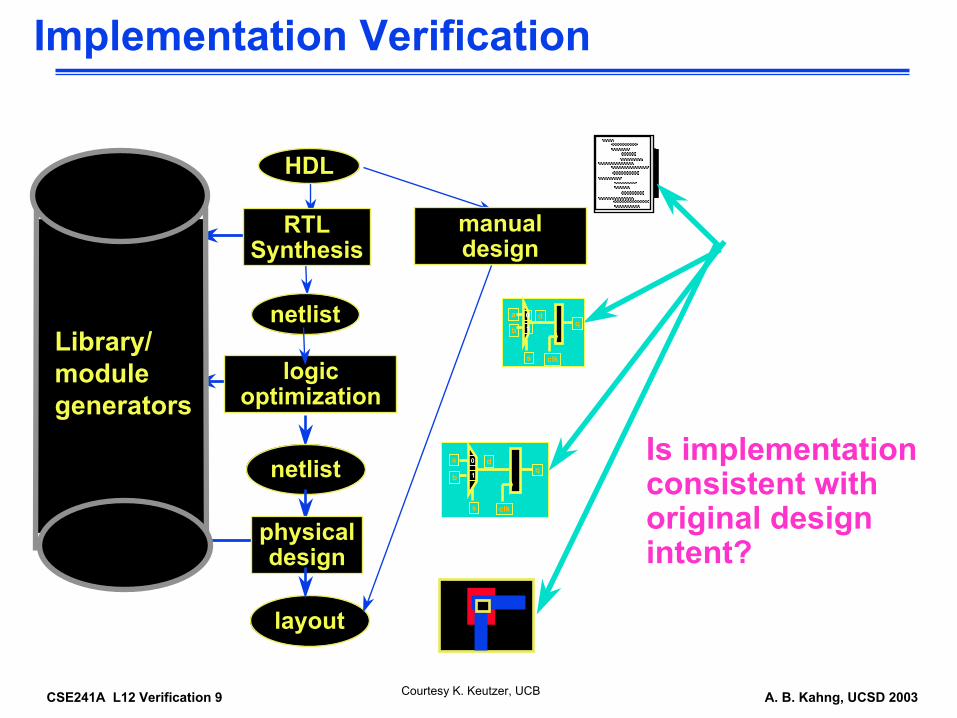
Implementation Verification
RTLSynthesis
HDL
netlist
logicoptimization
netlist
Library/modulegenerators
physicaldesign
layout
manualdesign
Is implementationconsistent with original design intent?
a
b
s
q0
1
d
clk
a
b
s
q0
1
d
clk
Courtesy K. Keutzer, UCB

CSE241A L12 Verification 10 A. B. Kahng, UCSD 2003
Manufacture Verification (Test)
RTLSynthesis
HDL
netlist
logicoptimization
netlist
Library/modulegenerators
physicaldesign
layout
manualdesign
Is manufacturedcircuit consistentwith implemented design?
a
b
s
q0
1
d
clk
a
b
s
q0
1
d
clk
Courtesy K. Keutzer, UCB

CSE241A L12 Verification 11 A. B. Kahng, UCSD 2003
Implementation Verification for ASICs
RTLSynthesis
HDL
netlist
logicoptimization
netlist
Library/modulegenerators
physicaldesign
layout
manualdesign
Apply gate-level simulation at each step to verify:
(1) functionality: 0-1 behavior on regression test set
(2) timing:maximum delay of circuit on critical paths
a
b
s
q0
1
d
clk
a
b
s
q0
1
d
clk
ASICsignoff
Courtesy K. Keutzer, UCB

CSE241A L12 Verification 12 A. B. Kahng, UCSD 2003
Advantages of gate-level simulationverifies timing and functionality simultaneouslyapproach well understood by designers
Disadvantages of gate-level simulation?computationally intensive - only 1 - 10 clock cycles of 100K gate design per 1 CPU secondincomplete - results only as good as your vector set - easy to overlook incorrect timing/behavior
Simulationdriver
(vectors)
Simulationmonitor(yes/no)
Software Simulation
a
b
s
q
0
1
d
clk
Courtesy K. Keutzer, UCB
CSE241A L12 Verification 13 A. B. Kahng, UCSD 2003
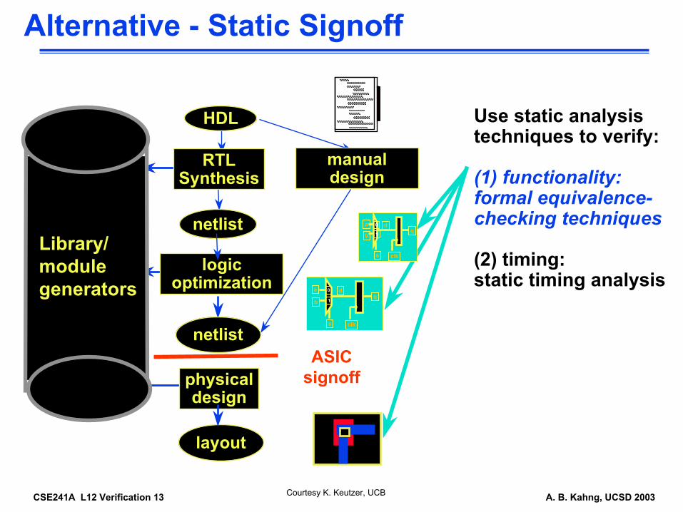
Alternative - Static Signoff
RTLSynthesis
HDL
netlist
logicoptimization
netlist
Library/modulegenerators
physicaldesign
layout
manualdesign
a
b
s
q0
1
d
clk
a
b
s
q0
1
d
clk
ASICsignoff
Use static analysis techniques to verify:
(1) functionality:formal equivalence-checking techniques
(2) timing:static timing analysis
Courtesy K. Keutzer, UCB
CSE241A L12 Verification 14 A. B. Kahng, UCSD 2003
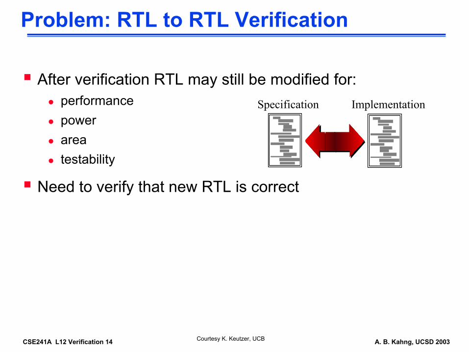
Problem: RTL to RTL Verification
After verification RTL may still be modified for:performancepowerareatestability
Need to verify that new RTL is correct
Specification Implementation
Courtesy K. Keutzer, UCB
CSE241A L12 Verification 15 A. B. Kahng, UCSD 2003
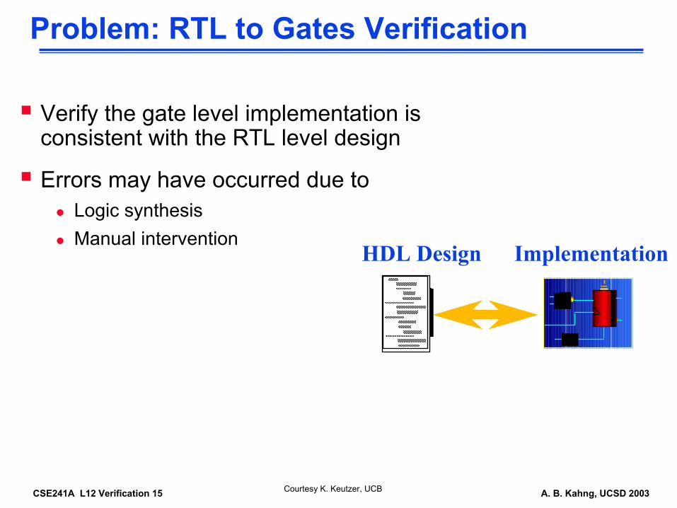
Problem: RTL to Gates Verification
Verify the gate level implementation is consistent with the RTL level design
Errors may have occurred due toLogic synthesisManual intervention
HDL Design Implementation
Courtesy K. Keutzer, UCB

CSE241A L12 Verification 16 A. B. Kahng, UCSD 2003
Problem: Gates to Gates Verification
Verify the modified gate level implementation is consistent with the RTL level design
Errors may have occurred due toIncorrect logic synthesis or module generationTest insertionScan chain reorderingClock tree synthesisPost layout “tweaks”
Netlist Implementation
Courtesy K. Keutzer, UCB

CSE241A L12 Verification 17 A. B. Kahng, UCSD 2003
Problem: Layout to Gates Verification (LVS)
Verify that modified gate level implementation is consistent with the RTL level design
Errors may have occurred due toErrors in physical design toolsManual changes in layout
Verification is primarily graphical or ``topological’’
netlist physical layout
Courtesy K. Keutzer, UCB
CSE241A L12 Verification 18 A. B. Kahng, UCSD 2003
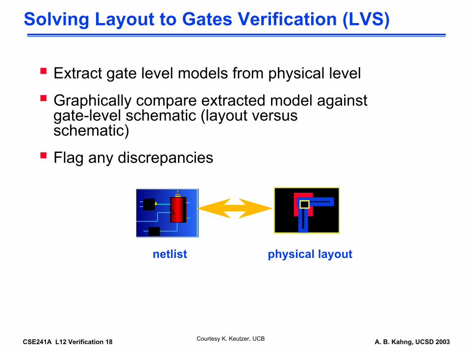
Solving Layout to Gates Verification (LVS)
Extract gate level models from physical level
Graphically compare extracted model against gate-level schematic (layout versus schematic)
Flag any discrepancies
netlist physical layout
Courtesy K. Keutzer, UCB

CSE241A L12 Verification 19 A. B. Kahng, UCSD 2003
Solving Gates to Gates Verification
clk
Combinationallogic
clk
Combinationallogic
clk
Combinationallogic
clk
Combinationallogic
clk
Combinationallogic
clk
Combinationallogic
“specification’’
implementationCourtesy K. Keutzer, UCB
CSE241A L12 Verification 20 A. B. Kahng, UCSD 2003
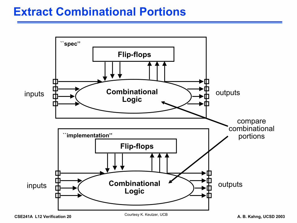
Extract Combinational Portions
comparecombinational
portions
``spec’’
Flip-flops
CombinationalLogic
inputs outputs
``implementation’’
Flip-flops
CombinationalLogic
inputs outputs
Courtesy K. Keutzer, UCB

CSE241A L12 Verification 21 A. B. Kahng, UCSD 2003
Combinational Equivalence Checking
Presumes equivalence relation given (or discovered) between sequential circuits
ApproachesCanonical forms - BDDs and variantsTest-oriented methodsSymbolic manipulation
- graph isomorphism- structural reductions
These techniques form the foundation of implementation verification
Courtesy K. Keutzer, UCB

CSE241A L12 Verification 22 A. B. Kahng, UCSD 2003
The Comparison Mitre
Primary Inputs, Register and Black Box Outputs
spec implementation
COMPARE
0 or 1
Courtesy K. Keutzer, UCB

CSE241A L12 Verification 23 A. B. Kahng, UCSD 2003
Verification and Testing
Given two single-output circuits A and B
Are A and B equivalent can be posed as: Is there a test for F s-a-0?
If F s-a-0 is redundant, A ≡ B else test vector produces different outputs for A and B.
x2
B
x4
x1
x3A
xs-a-0
Courtesy K. Keutzer, UCB
CSE241A L12 Verification 24 A. B. Kahng, UCSD 2003
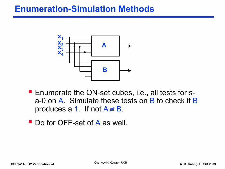
Enumeration-Simulation Methods
Enumerate the ON-set cubes, i.e., all tests for s-a-0 on A. Simulate these tests on B to check if Bproduces a 1. If not A ≡ B.
Do for OFF-set of A as well.
x2
B
x4
x1
x3A
Courtesy K. Keutzer, UCB
CSE241A L12 Verification 25 A. B. Kahng, UCSD 2003
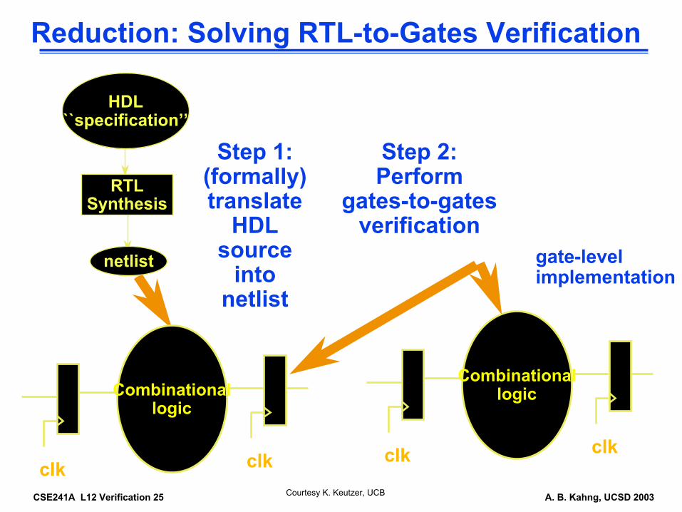
Reduction: Solving RTL-to-Gates Verification
RTLSynthesis
HDL``specification’’
netlist
Step 1: (formally) translate
HDL source
into netlist
Combinationallogic
clkclk
Combinationallogic
clkclk
Step 2: Perform
gates-to-gates verification
gate-levelimplementation
Courtesy K. Keutzer, UCB

CSE241A L12 Verification 26 A. B. Kahng, UCSD 2003
Reduction: Solving RTL-to-RTL Verification
RTLSynthesis
HDL``specification’’
netlist
Step 1: (formally) translateboth HDL sources
into netlists
Combinationallogic
clkclk
RTLSynthesis
HDLimplementation
netlist
Combinationallogic
clkclk
Step 2: perform gate-to-
gate verification on netlists
Courtesy K. Keutzer, UCB

CSE241A L12 Verification 27 A. B. Kahng, UCSD 2003
Equivalence Checking Summary
Routinely verify complex (>1M gate) integrated circuit designs
Commercial (e.g. Synopsys 44% market share, Verplex33%) and proprietary (e.g. IBM) solutions exist
Static sign-off methodology more widely used
Successful equivalence checkers orchestrate several different approaches
syntactic equivalence automatic test pattern generation-like approachesBDD-based techniquespattern-reduction methods
Open issuesretimed circuitscircuits with differing state assignments
Courtesy K. Keutzer, UCB

CSE241A L12 Verification 28 A. B. Kahng, UCSD 2003
Retimed Circuits
ab
s
q01
d
clk
a
b
s
q01
d
clk
Circuits are equivalent (modulo some initial state issues)but it is not possible to show that they are equivalent using Boolean equivalence
Courtesy K. Keutzer, UCB
CSE241A L12 Verification 29 A. B. Kahng, UCSD 2003
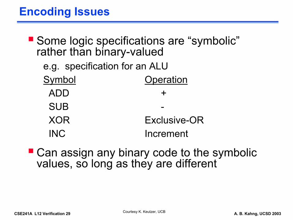
Encoding Issues
Some logic specifications are “symbolic” rather than binary-valued
e.g. specification for an ALUSymbol OperationADD +SUB -XOR Exclusive-ORINC Increment
Can assign any binary code to the symbolic values, so long as they are different
Courtesy K. Keutzer, UCB

CSE241A L12 Verification 30 A. B. Kahng, UCSD 2003
Different Encodings
Circuit 1Symbol OperationADD 00SUB 01XOR 10INC 11
Circuit 2Symbol OperationADD 11SUB 10XOR 00INC 01
Different encodingsmake circuits no longer amenable to combinational logic equivalence checking
Courtesy K. Keutzer, UCB

CSE241A L12 Verification 31 A. B. Kahng, UCSD 2003
Physical Verification

CSE241A L12 Verification 32 A. B. Kahng, UCSD 2003
Overview
What is Physical Verification (PV)?
General PV conceptsDesign Rule Check (DRC)Logical Versus Schematic (LVS)Verification Algorithms
- Flat and Hierarchical
ApproachesDRC
- Place and Route, Flat and HierarchicalLVS
- Place and Route, Flat and Hierarchical
Courtesy Cadence Design Systems, Inc.
CSE241A L12 Verification 33 A. B. Kahng, UCSD 2003
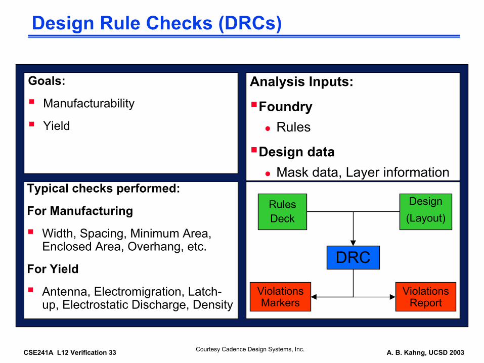
Design Rule Checks (DRCs)
Goals:
Manufacturability
Yield
Analysis Inputs:
FoundryRules
Design dataMask data, Layer information
Typical checks performed:
For Manufacturing
Width, Spacing, Minimum Area, Enclosed Area, Overhang, etc.
For Yield
Antenna, Electromigration, Latch-up, Electrostatic Discharge, Density
DRC
Violations Report
Violations Markers
Rules Deck
Design(Layout)
Courtesy Cadence Design Systems, Inc.
CSE241A L12 Verification 34 A. B. Kahng, UCSD 2003
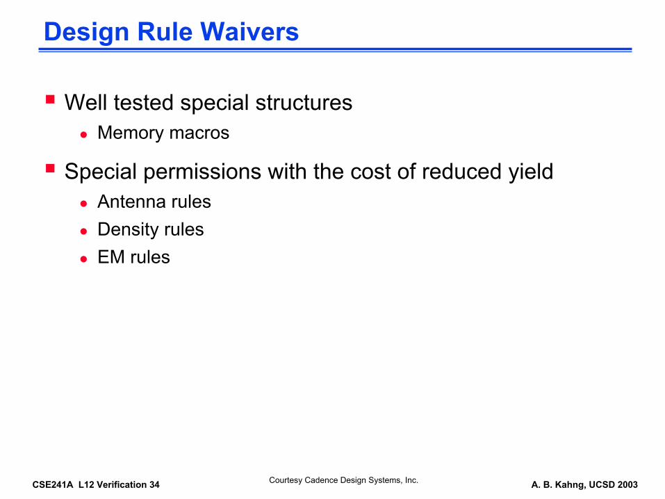
Design Rule Waivers
Well tested special structuresMemory macros
Special permissions with the cost of reduced yieldAntenna rulesDensity rulesEM rules
Courtesy Cadence Design Systems, Inc.
CSE241A L12 Verification 35 A. B. Kahng, UCSD 2003
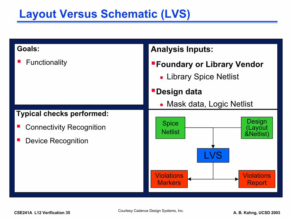
Layout Versus Schematic (LVS)
Goals:
Functionality
Analysis Inputs:
Foundary or Library VendorLibrary Spice Netlist
Design dataMask data, Logic Netlist
Typical checks performed:
Connectivity Recognition
Device Recognition
LVS
Violations Report
Violations Markers
Spice Netlist
Design (Layout &Netlist)
Courtesy Cadence Design Systems, Inc.

CSE241A L12 Verification 36 A. B. Kahng, UCSD 2003
Design Transistors:Design Layout:
Analysis Process
Steps: Design Netlist:
I1 I3
I2 I4IN1 IN1O1 O1
Net2Net1 Net3
IN1 O1
• From Gates to Transistors
• Primary I/Os Identified
• Connectivity Traced
• Device Recognition
Net1Net2
Net3
BA
VDD
GND
BA
VDD
GND
2/1
1/1
2/1
1/1
I1
I2
I3
I4
Net3Net1Net2
Courtesy Cadence Design Systems, Inc.
CSE241A L12 Verification 37 A. B. Kahng, UCSD 2003
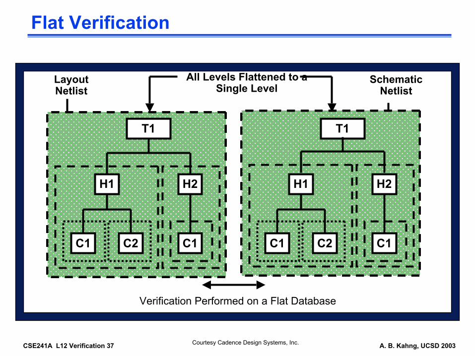
Flat Verification
Verification Performed on a Flat Database
T1
C1 C2 C1 C1
H2 H1
C2 C1
H2
T1
H1
All Levels Flattened to a Single Level
Schematic Netlist
Layout Netlist
T1
C1 C2 C1 C1
H2 H1
C2 C1
H2
T1
H1
T1
C1 C2 C1 C1
H2 H1
C2 C1
H2
T1
H1
T1
C1 C2 C1 C1
H2 H1
C2 C1
H2
T1
H1
T1
C1 C2 C1 C1
H2 H1
C2 C1
H2
T1
H1
Courtesy Cadence Design Systems, Inc.

CSE241A L12 Verification 38 A. B. Kahng, UCSD 2003
Hierarchical Verification
T1
C1 C2 C1 C1
H2 H1
C2 C1
H2
T1
H1
Schematic Netlist
Layout Netlist
Check Check
Check
Check Check
Cells VerifiedCells not verified since
C1 already checked
Cells VerifiedCells Verified
Top Level Verified
Skip Skip
T1
C1 C2
H2H1
Cells Verified
Courtesy Cadence Design Systems, Inc.
CSE241A L12 Verification 39 A. B. Kahng, UCSD 2003
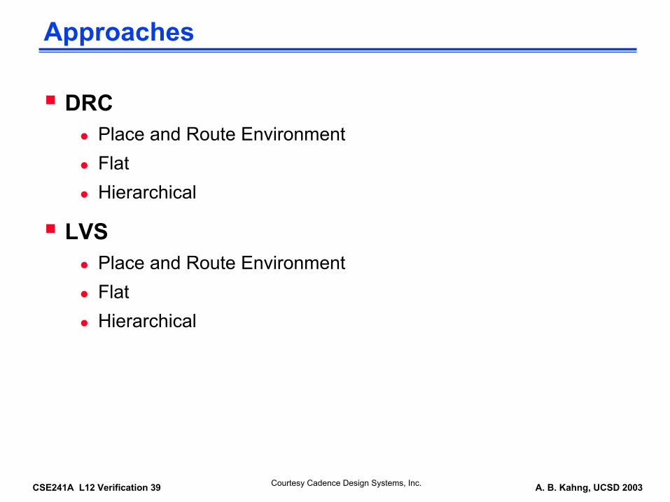
Approaches
DRCPlace and Route EnvironmentFlatHierarchical
LVSPlace and Route EnvironmentFlatHierarchical
Courtesy Cadence Design Systems, Inc.
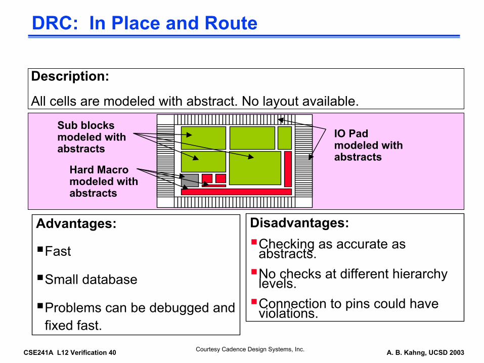
CSE241A L12 Verification 40 A. B. Kahng, UCSD 2003
DRC: In Place and Route
Advantages:
Fast
Small database
Problems can be debugged and fixed fast.
Disadvantages:Checking as accurate as abstracts.No checks at different hierarchy levels.Connection to pins could have violations.
Description:
All cells are modeled with abstract. No layout available.
IO Pad modeled with abstracts
Sub blocks modeled with abstracts
Hard Macro modeled with abstracts
Courtesy Cadence Design Systems, Inc.
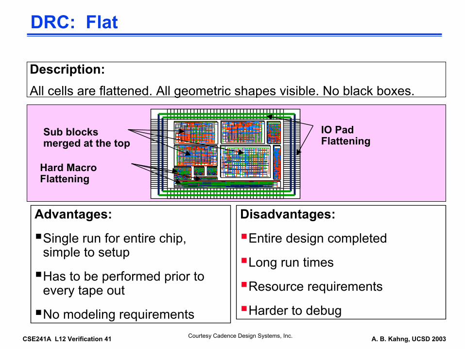
CSE241A L12 Verification 41 A. B. Kahng, UCSD 2003
DRC: Flat
Advantages:
Single run for entire chip, simple to setup
Has to be performed prior to every tape out
No modeling requirements
Disadvantages:
Entire design completed
Long run times
Resource requirements
Harder to debug
Description:All cells are flattened. All geometric shapes visible. No black boxes.
IO Pad Flattening
Sub blocks merged at the top
Hard Macro Flattening
Courtesy Cadence Design Systems, Inc.

CSE241A L12 Verification 42 A. B. Kahng, UCSD 2003
DRC: Hierarchical
Advantages:Start before entire chip completedSmaller data size = shorter run times, simpler debugging, easier to fixEarly density, EM, wide metal checks and repairEffects seen on timing, SI early when it can still be addressed
Disadvantages:Proper modeling of over the block and through the block routesFull flat chip analysis is still required Density checks may be inaccurateAssumptions made at hierarchy boundaries
Description:Bottom-up checking starting at block/hard macro level
Blocks verified separately
Top level verified using black box models for sub-blocks
Courtesy Cadence Design Systems, Inc.
CSE241A L12 Verification 43 A. B. Kahng, UCSD 2003
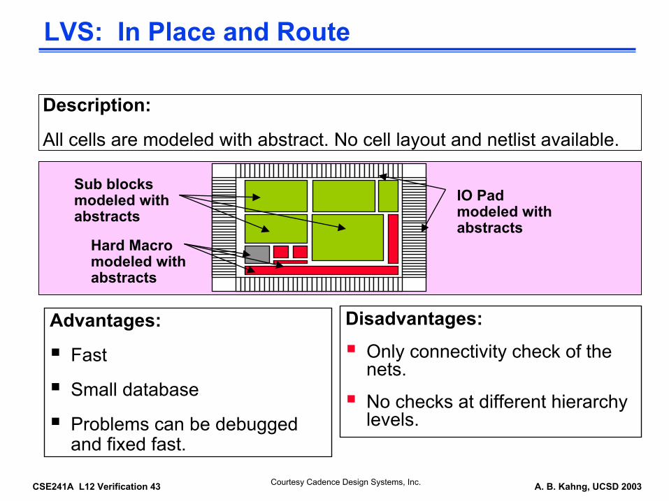
LVS: In Place and Route
Advantages:
Fast
Small database
Problems can be debugged and fixed fast.
Disadvantages:
Only connectivity check of the nets.
No checks at different hierarchy levels.
Description:
All cells are modeled with abstract. No cell layout and netlist available.
IO Pad modeled with abstracts
Sub blocks modeled with abstracts
Hard Macro modeled with abstracts
Courtesy Cadence Design Systems, Inc.

CSE241A L12 Verification 44 A. B. Kahng, UCSD 2003
LVS: Flat
Advantages:Simple setup, implementation
No modeling requirement
Run before all tape outs regardless
Disadvantages:Large data yielding long run times
Hard to debugging
Late in design cycle hard to accommodate changes
Description:Design flattened to one level.
Primary I/Os and supply I/Os labeled
Entire IC layout compared to transistor level schematic.
Courtesy Cadence Design Systems, Inc.
CSE241A L12 Verification 45 A. B. Kahng, UCSD 2003
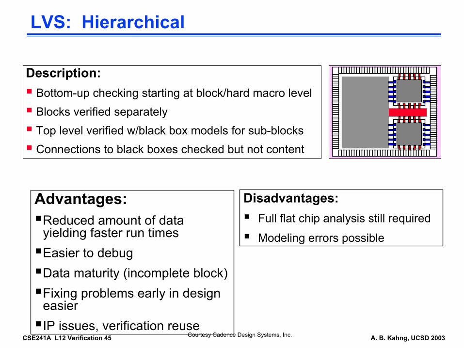
LVS: Hierarchical
Advantages:Reduced amount of data yielding faster run timesEasier to debugData maturity (incomplete block)Fixing problems early in design easierIP issues, verification reuse
Disadvantages:Full flat chip analysis still required
Modeling errors possible
Description:Bottom-up checking starting at block/hard macro levelBlocks verified separatelyTop level verified w/black box models for sub-blocksConnections to black boxes checked but not content
Courtesy Cadence Design Systems, Inc.

CSE241A L12 Verification 46 A. B. Kahng, UCSD 2003
Hierarchical Filling Problem
Filling geometries are added only to master cells
Two instances of a master cell
Original layout
features
Flat fill solution Hierarchical fill solution
Each cell of the filled layout is a filled version of the corresponding original master cell

CSE241A L12 Verification 47 A. B. Kahng, UCSD 2003
Why Hierarchical Filling?
Hierarchy characteristics of custom and semi-custom design flows
Enables and faster verification of the filled layout
Decreases data volume for standard cell designs

CSE241A L12 Verification 48 A. B. Kahng, UCSD 2003
Difficulties of Hierarchical Filling
Density constraints for all instances of the master
Interactions / interferences at master cell boundaries
Always worse than flat solutions

CSE241A L12 Verification 49 A. B. Kahng, UCSD 2003
k-way Master Cell Splitting
C1
Ci
C2
C2`C1`C1`C2`
Ci
C2C1
Ci,1Ci,2
C1`C2`
C2C1
C1`C2`
Ci,1 Ci,2
Create k copies of master cell Ci
k → ∞ : hierarchical layout → flat layout
C2`C1` C2`C1`
Link all contained master cell C` with the new copies of Ci
C1 C2
Randomly replace Ci in any master cell with one of the new copies

CSE241A L12 Verification 50 A. B. Kahng, UCSD 2003
Hybrid Hierarchical / Flat Filling
Purely hierarchical fill phase
Flat fill `cleanup` phase
Split-hierarchical phase
features
three instances of a master cell

CSE241A L12 Verification 51 A. B. Kahng, UCSD 2003
Physical Verification Summary
Tool modesHierarchical vs. Flat
Examining DRC and LVS errorsDesign rule waivers
DRC and LVS approachesPlace and RouteFlatHierarchical
Dummy fill insertionFlatHierarchical
Courtesy Cadence Design Systems, Inc.


