CSE331 W10&11.1 Irwin Fall 2007 PSU CSE 331 Computer Organization and Design Fall 2007 Week 10 & 11 Section 1: Mary Jane Irwin ( www.cse.psu.edu/~mji ) Section 2: Krishna Narayanan Course material on ANGEL: cms.psu.edu [adapted from D. Patterson slides]
Transcript
CSE331 W10&11.1 Irwin Fall 2007 PSU
CSE 331Computer Organization and
DesignFall 2007
Week 10 & 11
Section 1: Mary Jane Irwin (www.cse.psu.edu/~mji)
Section 2: Krishna Narayanan
Course material on ANGEL: cms.psu.edu
[adapted from D. Patterson slides]
CSE331 W10&11.2 Irwin Fall 2007 PSU
Head’s Up Last week’s material
Designing a MIPS single cycle datapath This week’s material and next week’s
More on single cycle datapath design and exam review- Reading assignment – PH: 5.4, B.8, C.1-C.2
Exam #1 take home solution due Thursday, Nov 1st (by 11:55pm) HW 7 is due Tuesday, Nov 27th (by 11:55pm) Quiz 6 closes Tuesday, Nov 5th (by 11:55pm) Exam #2 is Thursday, Nov 8th, 6:30 to 7:45pm
- People with conflicts should have sent email by now Friday, Nov 16th is the late-drop deadline Final Exam is Tuesday, Dec 18th, 10:10 to noon, 112 Walker
CSE331 W10&11.3 Irwin Fall 2007 PSU
Each MAS (microarchitectural specifications) included Pipeline and block diagrams Textual description of the theory of operation Unit inputs and outputs and protocols governing data
transfers Corner cases of the design that were especially tricky New circuits required for implementation Notes on testing and validation
The Pentium Chronicles, Colwell, pg. 82
CSE331 W10&11.4 Irwin Fall 2007 PSU
Review: Creating a Datapath from the Parts
Assemble the datapath elements, add control lines as needed, and design the control path
Fetch, decode and execute each instructions in one clock cycle – single cycle design
no datapath resource can be used more than once per instruction, so some must be duplicated (e.g., one reason why we have a separate Instruction Memory and Data Memory)
to share datapath elements between two different instruction classes need multiplexors at the input of the shared elements with control lines to do the selection
Cycle time is determined by length of the longest (slowest) path
CSE331 W10&11.5 Irwin Fall 2007 PSU
Review: A Simple MIPS Datapath Design
Write Data
Read Addr 1
Read Addr 2
Write Addr
Register
File
Read Data 1
Read Data 2
ALU
ovfzero
ALU controlRegWrite
DataMemory
Address
Write Data
Read Data
MemWrite
MemReadSign
Extend16 32
MemtoRegALUSrc
ReadAddress
Instruction
InstructionMemory
Add
PC
4 Shiftleft 2
Add
PCSrc
CSE331 W10&11.6 Irwin Fall 2007 PSU
Adding the Control Selecting the operations to perform (ALU, Register
File and Memory read/write) Controlling the flow of data (multiplexor inputs) Information comes from the 32 bits of the instruction
I-Type: op rs rt address offset
31 25 20 15 0
R-type:
31 25 20 15 5 0
op rs rt rd functshamt
10
Observations op field always
in bits 31-26 addr of two
registers to be read are always specified by the rs and rt fields (bits 25-21 and 20-16)
base register for lw and sw always in rs (bits 25-21) addr. of register to be written is in one of two places – in rt
(bits 20-16) for lw; in rd (bits 15-11) for R-type instructions offset for beq, lw, and sw always in bits 15-0
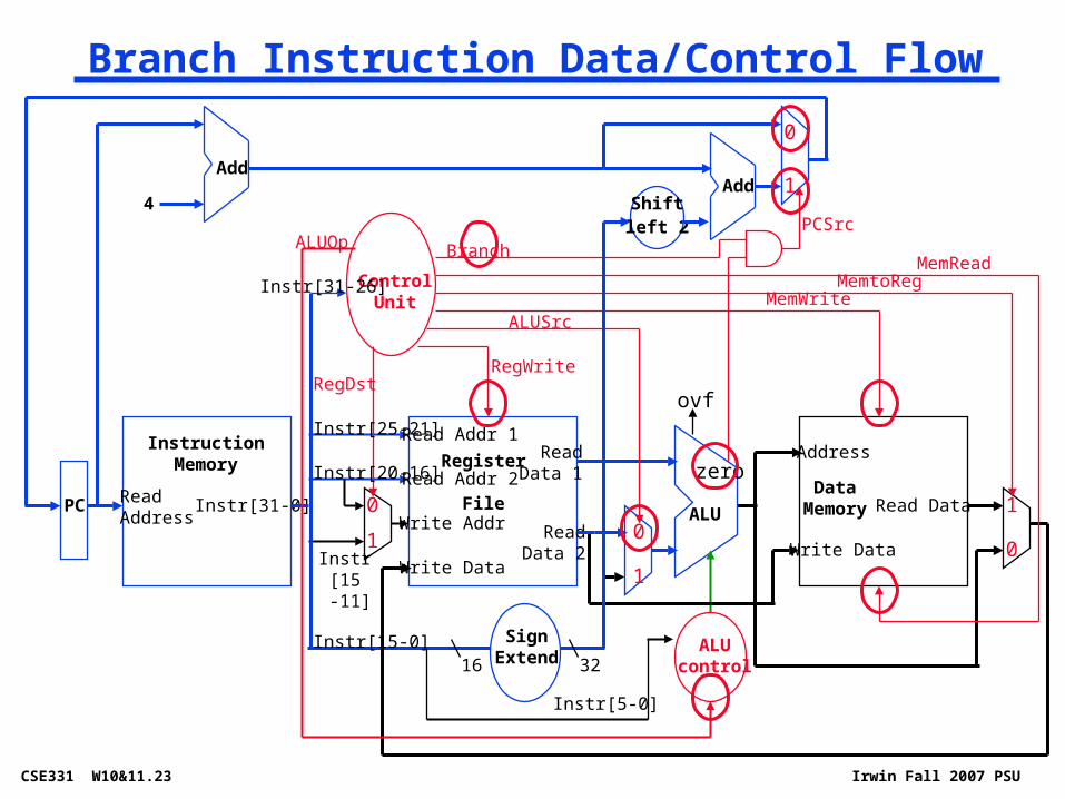
CSE331 W10&11.7 Irwin Fall 2007 PSU
(Almost) Complete Single Cycle Datapath
ReadAddress
Instr[31-0]
InstructionMemory
Add
PC
4
Write Data
Read Addr 1
Read Addr 2
Write Addr ALU
ovfzero
DataMemory
Address
Write Data
Read Data
MemWrite
MemRead
Register
File
Read Data 1
Read Data 2
RegWrite
SignExtend16 32
MemtoRegALUSrc
Shiftleft 2
Add
PCSrc
10
RegDst
0
1
10
1
0
ALUcontrol
ALUOpInstr[5-0]
Instr[15-0]
Instr[25-21]
Instr[20-16]
Instr[15 -11]
CSE331 W10&11.8 Irwin Fall 2007 PSU
ALU Control
ALU control input
Function
0000 and
0001 or
0010 xor
0011 nor
0110 add
1110 subtract
1111 set on less than
ALU's operation based on instruction type and function code
Notice that we are using different encodings than in the book
CSE331 W10&11.10 Irwin Fall 2007 PSU
ALU Control, Con’t Controlling the ALU uses of multiple decoding levels
main control unit generates the ALUOp bits ALU control unit generates ALUcontrol bits
Instr op funct ALUOp action ALUcontrol
lw xxxxxx 00
sw xxxxxx 00
beq xxxxxx 01
add 100000 10 add 0110
subt 100010 10 subtract 1110
and 100100 10 and 0000
or 100101 10 or 0001
xor 100110 10 xor 0010
nor 100111 10 nor 0011
slt 101010 10 slt 1111
add 0110
add 0110
subtract 1110
CSE331 W10&11.12 Irwin Fall 2007 PSU
ALU Control Truth TableF5 F4 F3 F2 F1 F0 ALU
Op1
ALU Op0
ALU control3
ALU control2
ALU control1
ALU control0
X X X X X X 0 0 0 1 1 0
X X X X X X 0 1 1 1 1 0
X X 0 0 0 0 1 0 0 1 1 0
X X 0 0 1 0 1 0 1 1 1 0
X X 0 1 0 0 1 0 0 0 0 0
X X 0 1 0 1 1 0 0 0 0 1
X X 0 1 1 0 1 0 0 0 1 0
X X 0 1 1 1 1 0 0 0 1 1
X X 1 0 1 0 1 0 1 1 1 1
Four, 6-input truth tables
Our ALU m control input
Add/subt Mux control
CSE331 W10&11.13 Irwin Fall 2007 PSU
ALU Control Logic From the truth table can design the ALU Control logicInstr[3]Instr[2]Instr[1]Instr[0]
Setting of the MemRd signal (for R-type, sw, beq) depends on the memory design
CSE331 W10&11.33 Irwin Fall 2007 PSU
Single Cycle Implementation Cycle Time
Unfortunately, though simple, the single cycle approach is not used because it is very slow
Clock cycle must have the same length for every instruction
What is the longest (slowest) path (slowest instruction)?
CSE331 W10&11.35 Irwin Fall 2007 PSU
Instruction Critical Paths
Instr. I Mem Reg Rd ALU Op D Mem Reg Wr Total
R-type
load
store
beq
jump
4 1 2 1 8
4 1 2 4 1 12
Calculate cycle time assuming negligible delays (for muxes, control unit, sign extend, PC access, shift left 2, wires, setup and hold times) except:
Instruction and Data Memory (4 ns)
ALU and adders (2 ns)
Register File access (reads or writes) (1 ns)
4 1 2 4 11
4 1 2 7
4 4
CSE331 W10&11.36 Irwin Fall 2007 PSU
Single Cycle Disadvantages & Advantages Uses the clock cycle inefficiently – the clock cycle
must be timed to accommodate the slowest instr especially problematic for more complex instructions like
floating point multiply
May be wasteful of area since some functional units (e.g., adders) must be duplicated since they can not be shared during a clock cycle
but It is simple and easy to understand
Clk
lw sw Waste
Cycle 1 Cycle 2
CSE331 W10&11.37 Irwin Fall 2007 PSU
Multicycle Implementation Overview Each instruction step takes 1 clock cycle
Therefore, an instruction takes more than 1 clock cycle to complete
Not every instruction takes the same number of clock cycles to complete
Multicycle implementations allow faster clock rates different instructions to take a different number of clock
cycles functional units to be used more than once per instruction
as long as they are used on different clock cycles, as a result
- only need one memory
- only need one ALU/adder
CSE331 W10&11.38 Irwin Fall 2007 PSU
The Multicycle Datapath – A High Level View
Address
Read Data(Instr. or Data)
Memory
PC
Write Data
Read Addr 1
Read Addr 2
Write Addr
Register
File
Read Data 1
Read Data 2
ALU
Write Data
IRM
DR
AB
AL
Uo
ut
Registers have to be added after every major functional unit to hold the output value until it is used in a subsequent clock cycle
CSE331 W10&11.39 Irwin Fall 2007 PSU
Clocking the Multicycle Datapath
Address
Read Data(Instr. or Data)
Memory
PC
Write Data
Read Addr 1
Read Addr 2
Write Addr
Register
File
Read Data 1
Read Data 2
ALU
Write Data
IRM
DR
AB
AL
Uo
ut
System Clock
MemWrite RegWrite
clock cycle
CSE331 W10&11.40 Irwin Fall 2007 PSU
Break up the instructions into steps where each step takes a clock cycle while trying to balance the amount of work to be done in each step use only one major functional unit per clock cycle
At the end of a clock cycle Store values needed in a later clock cycle by the current
instruction in a state element (internal register not visible to the programmer)
IR – Instruction RegisterMDR – Memory Data RegisterA and B – Register File read data registersALUout – ALU output register
- All (except IR) hold data only between a pair of adjacent clock cycles (so they don’t need a write control signal)
Data used by subsequent instructions are stored in programmer visible state elements (i.e., Register File, PC, or Memory)
Our Multicycle Approach
CSE331 W10&11.41 Irwin Fall 2007 PSU
The Complete Multicycle Data with Control
Address
Read Data(Instr. or Data)
Memory
PC
Write Data
Read Addr 1
Read Addr 2
Write Addr
Register
File
Read Data 1
Read Data 2
ALU
Write Data
IRM
DR
AB
AL
Uo
ut
SignExtend
Shiftleft 2 ALU
control
Shiftleft 2
ALUOpControl
IRWriteMemtoReg
MemWriteMemRead
IorD
PCWrite
PCWriteCond
RegDstRegWrite
ALUSrcAALUSrcB
zero
PCSource
1
1
1
1
1
10
0
0
0
0
0
2
2
3
4
Instr[5-0]
Instr[25-0]
PC[31-28]
Instr[15-0]
Instr[3
1-2
6]
32
28
CSE331 W10&11.42 Irwin Fall 2007 PSU
Review: Our ALU Control Controlling the ALU uses of multiple decoding levels
main control unit generates the ALUOp bits ALU control unit generates ALUcontrol bits
Instr op funct ALUOp action ALUcontrol
lw xxxxxx 00 add 0110
sw xxxxxx 00 add 0110
beq xxxxxx 01 subtract 1110
add 100000 10 add 0110
subt 100010 10 subtract 1110
and 100100 10 and 0000
or 100101 10 or 0001
xor 100110 10 xor 0010
nor 100111 10 nor 0011
slt 101010 10 slt 1111
CSE331 W10&11.43 Irwin Fall 2007 PSU
Reading from or writing to any of the internal registers, Register File, or the PC occurs (quickly) at the beginning (for read) or the end of a clock cycle (for write)
Reading from the Register File takes ~50% of a clock cycle since it has additional control and access overhead (but reading can be done in parallel with decode)
Had to add multiplexors in front of several of the functional unit input ports (e.g., Memory, ALU) because they are now shared by different clock cycles and/or do multiple jobs
All operations occurring in one clock cycle occur in parallel This limits us to one ALU operation, one Memory access,
Use PC to get instruction from the memory and put it in the Instruction Register
Increment the PC by 4 and put the result back in the PC
Can be described succinctly using the RTL "Register-Transfer Language“
IR = Memory[PC];PC = PC + 4;
Step 1: Instruction Fetch
Can we figure out the values of the control signals?
What is the advantage of updating the PC now?
CSE331 W10&11.47 Irwin Fall 2007 PSU
Datapath Activity During Instruction Fetch
Address
Read Data(Instr. or Data)
Memory
PC
Write Data
Read Addr 1
Read Addr 2
Write Addr
Register
File
Read Data 1
Read Data 2
ALU
Write Data
IRM
DR
AB
AL
Uo
ut
SignExtend
Shiftleft 2 ALU
control
Shiftleft 2
ALUOpControl
IRWriteMemtoReg
MemWriteMemRead
IorD
PCWrite
PCWriteCond
RegDstRegWrite
ALUSrcAALUSrcB
zero
PCSource
1
1
1
1
1
10
0
0
0
0
0
2
2
3
4
Instr[5-0]
Instr[25-0]
PC[31-28]
Instr[15-0]
Instr[3
1-2
6]
32
28
00
CSE331 W10&11.49 Irwin Fall 2007 PSU
Fetch Control Signals Settings
Start
Instr FetchIorD=0MemRead;IRWrite
ALUSrcA=0ALUsrcB=01
PCSource,ALUOp=00PCWrite
Unless otherwise assigned
PCWrite,IRWrite, MemWrite,RegWrite=0 others=X
CSE331 W10&11.50 Irwin Fall 2007 PSU
Don’t know what the instruction is yet, so can only Read registers rs and rt in case we need them Compute the branch address in case the instruction is a
branch The RTL:
A = Reg[IR[25-21]];B = Reg[IR[20-16]];ALUOut = PC +(sign-extend(IR[15-0])<< 2);
Note we aren't setting any control lines based on the instruction (since we don’t know what it is (the control logic is busy "decoding" the op code bits))
Step 2: Instruction Decode and Register Fetch
CSE331 W10&11.52 Irwin Fall 2007 PSU
Datapath Activity During Instruction Decode
Address
Read Data(Instr. or Data)
Memory
PC
Write Data
Read Addr 1
Read Addr 2
Write Addr
Register
File
Read Data 1
Read Data 2
ALU
Write Data
IRM
DR
AB
AL
Uo
ut
SignExtend
Shiftleft 2 ALU
control
Shiftleft 2
ALUOpControl
IRWriteMemtoReg
MemWriteMemRead
IorD
PCWrite
PCWriteCond
RegDstRegWrite
ALUSrcAALUSrcB
zero
PCSource
1
1
1
1
1
10
0
0
0
0
0
2
2
3
4
Instr[5-0]
Instr[25-0]
PC[31-28]
Instr[15-0]
Instr[3
1-2
6]
32
28
00
CSE331 W10&11.54 Irwin Fall 2007 PSU
Decode Control Signals Settings
Start
Instr Fetch Decode
ALUSrcA=0ALUSrcB=11ALUOp=00
PCWriteCond=0
IorD=0MemRead;IRWrite
ALUSrcA=0ALUsrcB=01
PCSource,ALUOp=00PCWrite
Unless otherwise assigned
PCWrite,IRWrite, MemWrite,RegWrite=0 others=X
CSE331 W10&11.55 Irwin Fall 2007 PSU
ALU is performing one of four functions, based on instruction type
Memory reference (lw and sw): ALUOut = A + sign-extend(IR[15-0]);
R-type: ALUOut = A op B;
Branch: if (A==B) PC = ALUOut; Jump: PC = PC[31-28] || (IR[25-0] << 2);
Step 3 (instruction dependent)
CSE331 W10&11.57 Irwin Fall 2007 PSU
Datapath Activity During lw & sw Execute
Address
Read Data(Instr. or Data)
Memory
PC
Write Data
Read Addr 1
Read Addr 2
Write Addr
Register
File
Read Data 1
Read Data 2
ALU
Write Data
IRM
DR
AB
AL
Uo
ut
SignExtend
Shiftleft 2 ALU
control
Shiftleft 2
ALUOpControl
IRWriteMemtoReg
MemWriteMemRead
IorD
PCWrite
PCWriteCond
RegDstRegWrite
ALUSrcAALUSrcB
zero
PCSource
1
1
1
1
1
10
0
0
0
0
0
2
2
3
4
Instr[5-0]
Instr[25-0]
PC[31-28]
Instr[15-0]
Instr[3
1-2
6]
32
28
00
CSE331 W10&11.59 Irwin Fall 2007 PSU
Datapath Activity During R-type Execute
Address
Read Data(Instr. or Data)
Memory
PC
Write Data
Read Addr 1
Read Addr 2
Write Addr
Register
File
Read Data 1
Read Data 2
ALU
Write Data
IRM
DR
AB
AL
Uo
ut
SignExtend
Shiftleft 2 ALU
control
Shiftleft 2
ALUOpControl
IRWriteMemtoReg
MemWriteMemRead
IorD
PCWrite
PCWriteCond
RegDstRegWrite
ALUSrcAALUSrcB
zero
PCSource
1
1
1
1
1
10
0
0
0
0
0
2
2
3
4
Instr[5-0]
Instr[25-0]
PC[31-28]
Instr[15-0]
Instr[3
1-2
6]
32
28
10
CSE331 W10&11.61 Irwin Fall 2007 PSU
Datapath Activity During beq Execute
Address
Read Data(Instr. or Data)
Memory
PC
Write Data
Read Addr 1
Read Addr 2
Write Addr
Register
File
Read Data 1
Read Data 2
ALU
Write Data
IRM
DR
AB
AL
Uo
ut
SignExtend
Shiftleft 2 ALU
control
Shiftleft 2
ALUOpControl
IRWriteMemtoReg
MemWriteMemRead
IorD
PCWrite
PCWriteCond
RegDstRegWrite
ALUSrcAALUSrcB
zero
PCSource
1
1
1
1
1
10
0
0
0
0
0
2
2
3
4
Instr[5-0]
Instr[25-0]
PC[31-28]
Instr[15-0]
Instr[3
1-2
6]
32
28
01
CSE331 W10&11.63 Irwin Fall 2007 PSU
Datapath Activity During j Execute
Address
Read Data(Instr. or Data)
Memory
PC
Write Data
Read Addr 1
Read Addr 2
Write Addr
Register
File
Read Data 1
Read Data 2
ALU
Write Data
IRM
DR
AB
AL
Uo
ut
SignExtend
Shiftleft 2 ALU
control
Shiftleft 2
ALUOpControl
IRWriteMemtoReg
MemWriteMemRead
IorD
PCWrite
PCWriteCond
RegDstRegWrite
ALUSrcAALUSrcB
zero
PCSource
1
1
1
1
1
10
0
0
0
0
0
2
2
3
4
Instr[5-0]
Instr[25-0]
PC[31-28]
Instr[15-0]
Instr[3
1-2
6]
32
28
CSE331 W10&11.65 Irwin Fall 2007 PSU
Execute Control Signals Settings
Start
Instr Fetch Decode
(Op = R-
type)
(Op =
beq)
(Op = lw or
sw) (Op = j)
ALUSrcA=1ALUSrcB=10ALUOp=00
PCWriteCond=0
ALUSrcA=1ALUSrcB=00ALUOp=10
PCWriteCond=0
ALUSrcA=1ALUSrcB=00ALUOp=01
PCSource=01PCWriteCond
PCSource=10PCWriteExecute
Unless otherwise assigned
PCWrite,IRWrite, MemWrite,RegWrite=0 others=X
ALUSrcA=0ALUSrcB=11ALUOp=00
PCWriteCond=0
IorD=0MemRead;IRWrite
ALUSrcA=0ALUsrcB=01
PCSource,ALUOp=00PCWrite
CSE331 W10&11.66 Irwin Fall 2007 PSU
Where We are Headed After Exam #2 Finish the design of the multi-cycle machine
Step 4 and step 5 data path design control path design for the multi-cycle machine a microprogramming approach for control path design