1464 JOURNAL OF MICROELECTROMECHANICAL SYSTEMS, VOL. 21, NO. 6, DECEMBER 2012
Design and Demonstration of an In-PlaneSilicon-on-Insulator Optical MEMSFabry–Pérot-Based Accelerometer
Integrated With Channel WaveguidesKazem Zandi, Joseph André Bélanger, and Yves-Alain Peter, Senior Member, IEEE
Abstract—In this paper, we present a novel optical microelec-tromechanical systems (MEMS) accelerometer sensor dedicatedto space applications. An in-plane Fabry–Pérot (FP) microcavity(FPM) with two distributed Bragg reflectors (DBRs) is used todetect the acceleration. One of the DBR mirrors is attached to twosuspended proof masses, allowing the FP gap to change while proofmasses experience acceleration. Acceleration is then detected bymeasuring the spectral shift of the FPM. The optical accelerom-eter presented here uses silicon strip waveguides integrated withMEMS on a single silicon-on-insulator wafer, making it compactand robust. All of the device components are fabricated using onesingle fabrication step. Immunity to electromagnetic interference,high sensitivity and resolution capability, integrability, reliability,low cross-sensitivity, simple fabrication, and possibility of havingtwo- and three-axis sensitivities are numerous advantages of oursensor compared to the conventional ones. The sensor perfor-mance demonstrated a 90-nm/g sensitivity and 111-μg resolutionand better than 250-mg dynamic range. [2012-0098]
Index Terms—Distributed Bragg reflector (DBR), Fabry–Pérot(FP), optical accelerometer, silicon-on-insulator (SOI),waveguides.
I. INTRODUCTION
M ICROELECTROMECHANICAL systems (MEMS) ca-pacitance accelerometers are currently used in space-
craft navigation systems [1], but they suffer from low SNR(which limits their sensitivity), high power consumption, tem-perature dependence, and high cross-sensitivity and are notimmune to electromagnetic interference [2], making them un-suitable for microsatellite applications.
Optical MEMS sensors are frequently used for industrialprocess, aerospace, and military application owing to theirimmunity to electromagnetic interference and possibility ofoperation in hazardous and high-temperature environments [3].
Manuscript received April 23, 2012; revised July 10, 2012; accepted July 13,2012. Date of publication August 27, 2012; date of current version November27, 2012. This work was supported in part by the Canadian Space Agency.An earlier version of this paper was presented at the 23rd lEEE Conference onMicro Electro Mechanical Systems, Hong Kong, China, January 24–28, 2010.Subject Editor S. Merlo.
Color versions of one or more of the figures in this paper are available onlineat http://ieeexplore.ieee.org.
Digital Object Identifier 10.1109/JMEMS.2012.2211577
Optical accelerometers have been investigated previously.Most of them are based on variable optical attenuator [4]–[6],optical diffraction detection [7], [8], antiresonant reflecting op-tical waveguides [2], Fresnel diffractive microlens [9], photoe-lastic effect [10], or wavelength dependence [11]. Out-of-planeMOEMS accelerometers based on light reflectance spectrumvariation were also reported where the reflectance spectrum ofa photonic band gap structure changes as a function of externalaccelerations [12], [13]. Some of the reported accelerometersare based on the combination of optical fibers and microma-chined silicon [4]–[6], [11], [14]. In some cases, they have lowsensitivity due to the low reflectivity of the Fabry–Pérot (FP)mirrors [11], [14]. Although, in some cases, they can be verysensitive [6], [7], they are not fully integrated, and they have alimited reliability because of their misalignment sensitivity tovibration/shock. μg-resolution optical accelerometers based onFP were demonstrated, but they are out of plane, not integrated,large in size, and expensive to fabricate, making them inappro-priate for microsatellite missions [15].
Over the last decade, small satellites and their applicationtoward space science missions have increased. Their need forattitude control necessities have developed toward full three-axis stabilization and precise pointing knowledge and control.This is associated with the requirement for compact low-power accelerometers and gyroscopes. Therefore, achieving anintegrated high-performance low-cost miniature sensor chip isdesired to reduce the spacecraft operating costs and to improvethe system performance for mission accomplishment and au-tonomous navigation.
Microphotonic integrated circuits are composed of two ormore photonic devices on a single substrate. The main diffi-culty that microphotonics should solve is system integration.Integrating different optical components on a single substratewill reduce the amount of external fiber-optic interconnections,consequently decreasing the overall system mass and size, andalso optimize the system reliability as well as cost efficiency.
Silicon photonics can bring together both conventional in-tegrated optics using ridge waveguides of several micrometersin cross section and nanophotonics structures where silicon-on-insulator (SOI) is used as platform. Using the SOI platform hastwo advantages; first, it decreases the size of integrated opticalstructures due to the high refractive index contrast between sili-con and air, and second, it is compatible with CMOS technology.
ZANDI et al.: DESIGN AND DEMONSTRATION OF IN-PLANE SOI OPTICAL MEMS FP-BASED ACCELEROMETER 1465
Here, we present a novel in-plane waveguide-integrated opti-cal MEMS accelerometer fabricated on SOI wafer. Our deviceis based on an FP filter with distributed Bragg reflector (DBR)mirrors utilizing strip silicon waveguides. The device can beintegrated with other optical functions since the structure is inplane, it is robust and reliable since only MEMS structures areused in the sensor part, it is sensitive since an FP interferometerwith relatively high reflectivity mirrors are used as the sensorpart, and it is a low-cost device since all the sensor componentsare fabricated in one simple fabrication step.
The aim of this work is to achieve a low-power, small-size,simple-fabrication, high-performance, and reliable navigationsensor for low-cost future small satellites/spacecrafts.
II. PRINCIPLE OF OPERATION
Fig. 1(a) shows the schematic of our proposed optical ac-celerometer. The device is based on an in-plane FP microcavity(FPM) with two DBR mirrors utilizing strip silicon waveg-uides, in which one DBR mirror is attached to two suspendedproof masses. As a consequence of acceleration, the relativedisplacement of the movable mirror with respect to the fixedone changes the cavity length and modifies the FP resonance[Fig. 1(b) and (c)].
A. Principle of Optical Detection
The resonance wavelength peak λ of an FPM with air gap isdirectly related to the gap x by [Fig. 1(b)]
x =mλ
2(1)
where m is the order of the resonance.The static response of an accelerometer with a suspended
mass of M (proof mass) and spring constant of k is definedby combining Newton’s second law and Hook’s law and isgiven by
a = − k
MΔx = −ω2
nΔx (2)
where a is the acceleration, ωn is the natural frequency ofthe system in the sensing direction, and Δx is the relativedisplacement of the suspended mass (movable DBR mirror)with respect to the fixed parts of the structure [Fig. 1(b)].
The relationship equation between the FPM accelerationsensor output and its experienced acceleration is then given bycombining (1) and (2)
a = −mω2nΔλ
2(3)
where Δλ is the FPM spectral shift. It can be seen fromthis relationship that the sensitivity and resolution of the de-vice are controlled by the optical (Δλ) and mechanical (ωn)characteristics.
Fig. 1. (a) Schematic of the accelerometer based on FP filter. (b) Schematicof the FPM made of two DBR mirrors. (c) Transmission spectrum shift of theFPM due to the 48-nm displacement of one mirror.
B. Mechanical Sensor Model
The accelerometer is symmetrical and consists of two proofmasses suspended by eight serpentine flexure beams [Fig. 1(a)].Accelerations parallel to the wafer plane and perpendicular tothe DBR mirrors cause the proof masses to move in the waferplane. The static response of such a suspended mass in they-direction is defined by (2)
a = − kyM
Δy = −ω2nyΔy (4)
where M is the proof mass, Δy is the proof mass displacementin the y-direction, ky is the device spring stiffness in they-direction, and ωny is the natural frequency of the system inthe y-direction.
1466 JOURNAL OF MICROELECTROMECHANICAL SYSTEMS, VOL. 21, NO. 6, DECEMBER 2012
Fig. 2. Simulated first four modes of the device: (a) Normal mode (resonant at 409 Hz). (b) Second mode (resonant at 3.48 kHz). (c) Third mode or trunnionmode (resonant at 3.53 kHz). (d) Fourth mode (resonant at 3.82 kHz). The arrows in the pictures show the displacement (or rotation) for each mode.
Using basic beam theory, the spring constants of a fixed-endbeam with length l, width w, and thickness t are given by
ky =Etw3
l3(5)
kx =2Etw
l(6)
kz =Ewt3
l3(7)
where E is Young’s modulus (∼160 GPa for silicon).A serpentine flexure beam consists of two span beams
and three connector beams. The considered dimensions forits components are as follows: span beam length: 470 μm,span beam width: 3 μm, and connector beam width =connector beam length = 10 μm.
Since the width of the connector beams is much larger thanthe width of the span beams, we can consider a serpentineflexure beam as a serial of two fixed-end beams. The effectivespring constant ks of two springs that are connected in series isthen given by
1
ks=
1
k1+
1
k2=
2
ki⇒ ks =
k12
=Etw3
2l3= 0.62 N/m (8)
where k1 and k2 are the spring constants of two fixed-endbeams which are equal in this case. Since the device consistsof eight serpentine springs in parallel, the total effective springconstant of the device is ktot = 8ks = 4.8 N/m.
The spring constant of the device was simulated by finite-element modeling using Coventorware 2010 and found to beK = 6.125 N/m. The difference between theory and simulationoriginates from the estimation we have made for the serpentinespring.
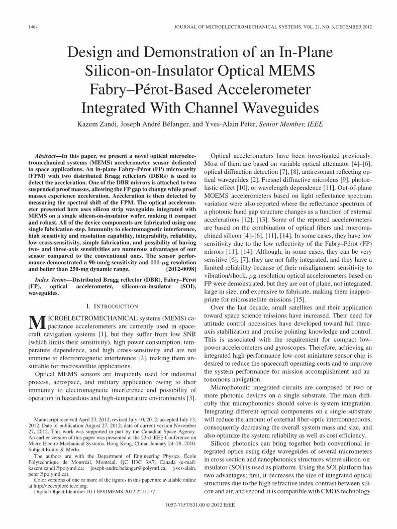
The main challenge in designing accelerometers is the man-ufacturing of a sensor which is sensitive to acceleration inthe desired direction but insensitive to all other cross-axisdirections. The cross-sensitivity of the device is investigatedusing mode analysis. Fig. 2 shows the first four possible modesof the structure. Owing to the optical characteristics, the sensoris insensitive to excitations that result in parallel motion of theBragg mirrors (modes 2 and 4) since the length of the FPMremains unchanged. However, it is sensitive to the angular ortrunnion deflection (mode 3) since the optical path of light inthe FPM changes in this case [Fig. 3(b)]. Although, under theexcitation of the resonant trunnion mode, no wavelength shiftis generated, the transmitted power through the device at theresonant wavelength is modulated due to the finesse reductionof the microcavity caused from parallelism deviation [16].Since the frequency of this mode is well above the sensor
ZANDI et al.: DESIGN AND DEMONSTRATION OF IN-PLANE SOI OPTICAL MEMS FP-BASED ACCELEROMETER 1467
Fig. 3. Two expected sensitive modes for the sensor. (a) Normal mode.(b) Trunnion mode.
Fig. 4. Simulated frequency response of the system for the (Mode 1) normaland (Mode 3) trunnion modes.
working bandwidth, it can be suppressed over the sensingbandwidth.
Fig. 4 represents the simulated frequency response of thesystem for normal and trunnion modes.
III. FABRICATION
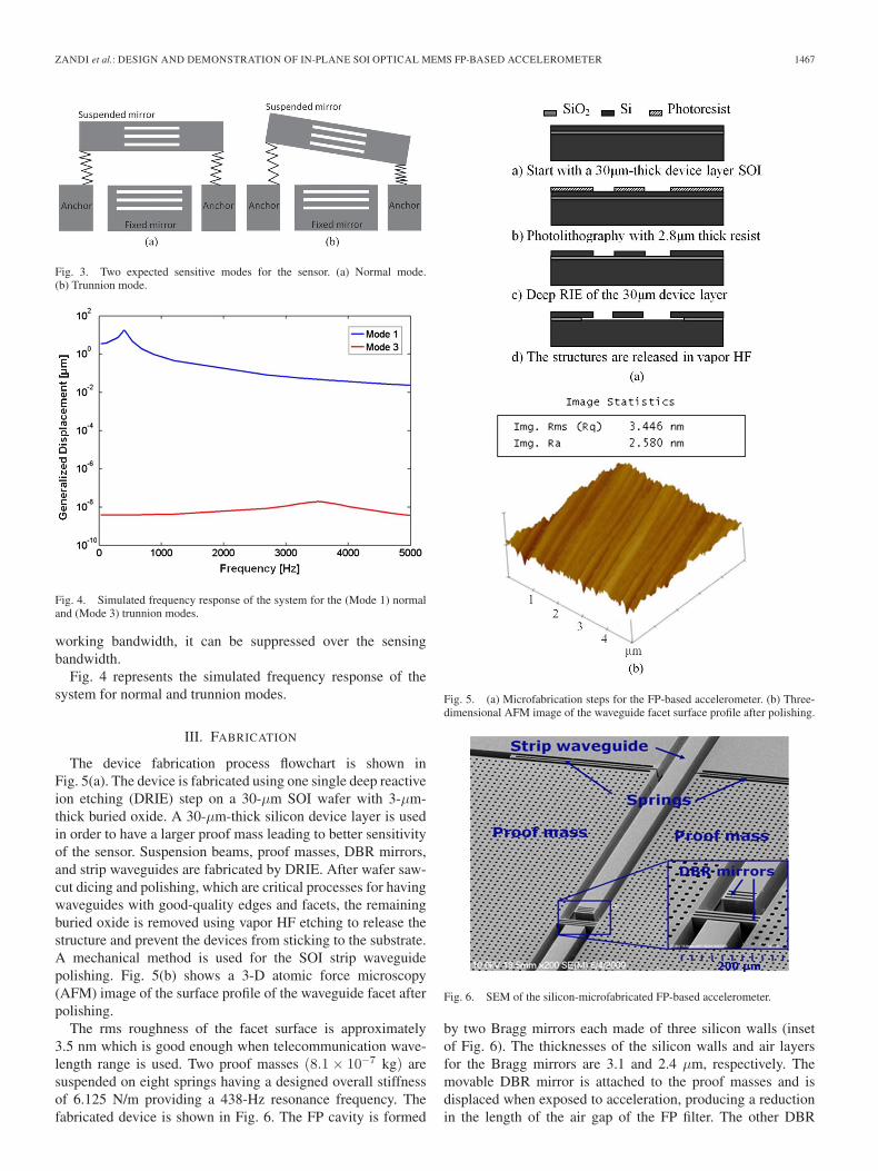
The device fabrication process flowchart is shown inFig. 5(a). The device is fabricated using one single deep reactiveion etching (DRIE) step on a 30-μm SOI wafer with 3-μm-thick buried oxide. A 30-μm-thick silicon device layer is usedin order to have a larger proof mass leading to better sensitivityof the sensor. Suspension beams, proof masses, DBR mirrors,and strip waveguides are fabricated by DRIE. After wafer saw-cut dicing and polishing, which are critical processes for havingwaveguides with good-quality edges and facets, the remainingburied oxide is removed using vapor HF etching to release thestructure and prevent the devices from sticking to the substrate.A mechanical method is used for the SOI strip waveguidepolishing. Fig. 5(b) shows a 3-D atomic force microscopy(AFM) image of the surface profile of the waveguide facet afterpolishing.
The rms roughness of the facet surface is approximately3.5 nm which is good enough when telecommunication wave-length range is used. Two proof masses (8.1× 10⁻⁷ kg) aresuspended on eight springs having a designed overall stiffnessof 6.125 N/m providing a 438-Hz resonance frequency. Thefabricated device is shown in Fig. 6. The FP cavity is formed
Fig. 5. (a) Microfabrication steps for the FP-based accelerometer. (b) Three-dimensional AFM image of the waveguide facet surface profile after polishing.
Fig. 6. SEM of the silicon-microfabricated FP-based accelerometer.
by two Bragg mirrors each made of three silicon walls (insetof Fig. 6). The thicknesses of the silicon walls and air layersfor the Bragg mirrors are 3.1 and 2.4 μm, respectively. Themovable DBR mirror is attached to the proof masses and isdisplaced when exposed to acceleration, producing a reductionin the length of the air gap of the FP filter. The other DBR
1468 JOURNAL OF MICROELECTROMECHANICAL SYSTEMS, VOL. 21, NO. 6, DECEMBER 2012
Fig. 7. Optical setup for the characterization of the accelerometer.
mirror is positioned at the end of a waveguide collimator. Thewaveguide collimator is used to reduce the numerical apertureof the beam in the horizontal direction, reducing the divergenceof the input beam. A gap of 27 μm was considered for the FPcavity to enable its future interrogation using a tunable laserwith a 30-nm dynamic range. Due to the sidewall scallopingphenomenon generated by the DRIE process, the sidewallsurfaces of the DBR mirrors are not very smooth. A smoothsidewall morphology is essential to minimize light scattering(which generates optical losses and reduces the quality factor ofthe cavity) and preserve collimated light beam when the etchedsidewall is used as a mirror surface. The rms surface roughnessof the DBR sidewalls was estimated to be 50 nm from thescanning electron micrograph (SEM) pictures. Adding oxygengas during the etching reduces the roughness [17]. Applyingthis technique to our device diminished the sidewall roughnessto 30 nm.
IV. CHARACTERIZATION
The same experimental setup as our previous report [18] isused to characterize the sensor (Fig. 7). Light from a broadbandsource (1520–1620 nm) is butt coupled to the input waveguidethrough an optical fiber. The transmitted light is collected by anoutput optical fiber butt coupled to the output tapered waveg-uide and sent to an optical spectrum analyzer. The whole setupis attached to an inclinable board that can be tilted. Accelerationis applied to the device as a consequence of gravity by tiltingthe board (g sin θ). The transmission peak of the FP shifts toshorter wavelengths, while the angle of inclination is increased(sensing accelerations from 0.180 to 0.307 g). Fig. 8 comparesthe measured and simulated transmission spectra of the device.
The initial transmission peak is 1534.5 nm, while 0.18-gacceleration is applied. As acceleration is increased, the airgap between the two Bragg reflectors decreases, resulting intransmission peak shift toward shorter wavelengths. We believethat the presence of sidebands can be due to the formation
Fig. 8. (Colored curves) Measured and (black-dashed curves) simulated trans-mission spectra of the FP-based accelerometer for various accelerations.
of FP cavities between input/output fiber end facet and input/output waveguide end facet and misalignments (between fiberand waveguide) after tilting the setup. The filter can be tunedcontinuously over 30 nm. A larger tuning range could beachieved using a smaller gap since it would provide a largerfree spectral range (FSR). The full-width at half-maximum ofthe peaks is 3 nm. A transfer matrix method is used to simulatethe transmitted light across the FP filter by considering aplane wave incident beam. Due to the fabrication imperfections(generated by photolithography and etching processes), themeasured peaks are not exactly located at the same locationspredicted by the simulations.
V. PERFORMANCE
A. Sensor Dynamic Range
Several optical resonances are available in the spectral re-sponse of FP-based sensors. The dynamic range of the deviceis limited to the half symmetric optical range between twoadjacent resonances or FSR; therefore, from (3), the maximumdynamic range is calculated as
Δamax =mω2
n
2× FSR
2· (9)
Knowing that the FPM resonance order for a 27-μm gap ism = 52, the maximum dynamic range of the sensor would beΔamax = 263 mg.
B. Sensor Sensitivity
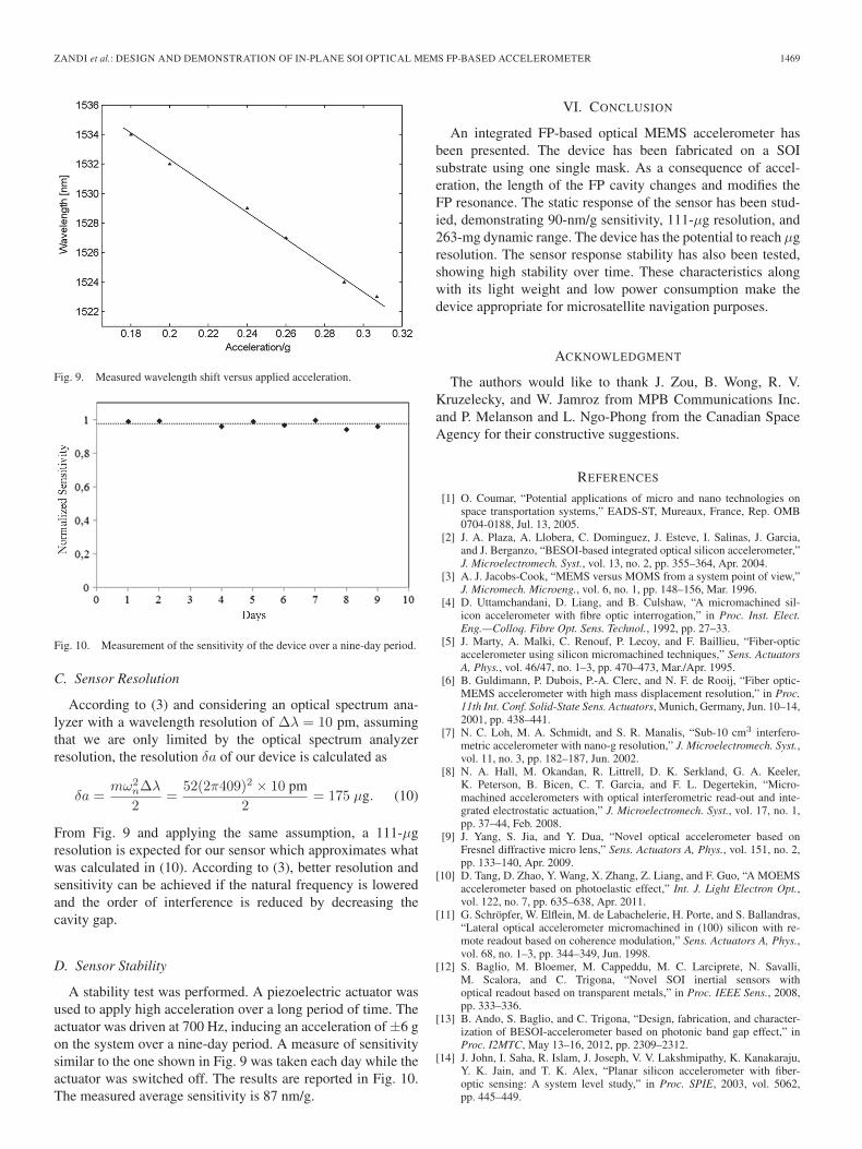
According to (2), the sensitivity of the sensor depends ontwo factors: mechanical part (ωn) which is related to the sensorarchitecture and optical part (Δλ) which is related to the FPfinesse. Fig. 9 shows the resonant wavelength shift of the FPMversus applied acceleration extracted from Fig. 8, yielding asensitivity of 90 nm/g.
ZANDI et al.: DESIGN AND DEMONSTRATION OF IN-PLANE SOI OPTICAL MEMS FP-BASED ACCELEROMETER 1469
Fig. 9. Measured wavelength shift versus applied acceleration.
Fig. 10. Measurement of the sensitivity of the device over a nine-day period.
C. Sensor Resolution
According to (3) and considering an optical spectrum ana-lyzer with a wavelength resolution of Δλ = 10 pm, assumingthat we are only limited by the optical spectrum analyzerresolution, the resolution δa of our device is calculated as
δa =mω2
nΔλ
2=
52(2π409)2 × 10 pm2
= 175 μg. (10)
From Fig. 9 and applying the same assumption, a 111-μgresolution is expected for our sensor which approximates whatwas calculated in (10). According to (3), better resolution andsensitivity can be achieved if the natural frequency is loweredand the order of interference is reduced by decreasing thecavity gap.
D. Sensor Stability
A stability test was performed. A piezoelectric actuator wasused to apply high acceleration over a long period of time. Theactuator was driven at 700 Hz, inducing an acceleration of ±6 gon the system over a nine-day period. A measure of sensitivitysimilar to the one shown in Fig. 9 was taken each day while theactuator was switched off. The results are reported in Fig. 10.The measured average sensitivity is 87 nm/g.
VI. CONCLUSION
An integrated FP-based optical MEMS accelerometer hasbeen presented. The device has been fabricated on a SOIsubstrate using one single mask. As a consequence of accel-eration, the length of the FP cavity changes and modifies theFP resonance. The static response of the sensor has been stud-ied, demonstrating 90-nm/g sensitivity, 111-μg resolution, and263-mg dynamic range. The device has the potential to reach μgresolution. The sensor response stability has also been tested,showing high stability over time. These characteristics alongwith its light weight and low power consumption make thedevice appropriate for microsatellite navigation purposes.
ACKNOWLEDGMENT
The authors would like to thank J. Zou, B. Wong, R. V.Kruzelecky, and W. Jamroz from MPB Communications Inc.and P. Melanson and L. Ngo-Phong from the Canadian SpaceAgency for their constructive suggestions.
REFERENCES
[1] O. Coumar, “Potential applications of micro and nano technologies onspace transportation systems,” EADS-ST, Mureaux, France, Rep. OMB0704-0188, Jul. 13, 2005.
[2] J. A. Plaza, A. Llobera, C. Dominguez, J. Esteve, I. Salinas, J. Garcia,and J. Berganzo, “BESOI-based integrated optical silicon accelerometer,”J. Microelectromech. Syst., vol. 13, no. 2, pp. 355–364, Apr. 2004.
[3] A. J. Jacobs-Cook, “MEMS versus MOMS from a system point of view,”J. Micromech. Microeng., vol. 6, no. 1, pp. 148–156, Mar. 1996.
[4] D. Uttamchandani, D. Liang, and B. Culshaw, “A micromachined sil-icon accelerometer with fibre optic interrogation,” in Proc. Inst. Elect.Eng.—Colloq. Fibre Opt. Sens. Technol., 1992, pp. 27–33.
[5] J. Marty, A. Malki, C. Renouf, P. Lecoy, and F. Baillieu, “Fiber-opticaccelerometer using silicon micromachined techniques,” Sens. ActuatorsA, Phys., vol. 46/47, no. 1–3, pp. 470–473, Mar./Apr. 1995.
[6] B. Guldimann, P. Dubois, P.-A. Clerc, and N. F. de Rooij, “Fiber optic-MEMS accelerometer with high mass displacement resolution,” in Proc.11th Int. Conf. Solid-State Sens. Actuators, Munich, Germany, Jun. 10–14,2001, pp. 438–441.
[7] N. C. Loh, M. A. Schmidt, and S. R. Manalis, “Sub-10 cm3 interfero-metric accelerometer with nano-g resolution,” J. Microelectromech. Syst.,vol. 11, no. 3, pp. 182–187, Jun. 2002.
[8] N. A. Hall, M. Okandan, R. Littrell, D. K. Serkland, G. A. Keeler,K. Peterson, B. Bicen, C. T. Garcia, and F. L. Degertekin, “Micro-machined accelerometers with optical interferometric read-out and inte-grated electrostatic actuation,” J. Microelectromech. Syst., vol. 17, no. 1,pp. 37–44, Feb. 2008.
[9] J. Yang, S. Jia, and Y. Dua, “Novel optical accelerometer based onFresnel diffractive micro lens,” Sens. Actuators A, Phys., vol. 151, no. 2,pp. 133–140, Apr. 2009.
[10] D. Tang, D. Zhao, Y. Wang, X. Zhang, Z. Liang, and F. Guo, “A MOEMSaccelerometer based on photoelastic effect,” Int. J. Light Electron Opt.,vol. 122, no. 7, pp. 635–638, Apr. 2011.
[11] G. Schröpfer, W. Elflein, M. de Labachelerie, H. Porte, and S. Ballandras,“Lateral optical accelerometer micromachined in (100) silicon with re-mote readout based on coherence modulation,” Sens. Actuators A, Phys.,vol. 68, no. 1–3, pp. 344–349, Jun. 1998.
[12] S. Baglio, M. Bloemer, M. Cappeddu, M. C. Larciprete, N. Savalli,M. Scalora, and C. Trigona, “Novel SOI inertial sensors withoptical readout based on transparent metals,” in Proc. IEEE Sens., 2008,pp. 333–336.
[13] B. Ando, S. Baglio, and C. Trigona, “Design, fabrication, and character-ization of BESOI-accelerometer based on photonic band gap effect,” inProc. I2MTC, May 13–16, 2012, pp. 2309–2312.
[14] J. John, I. Saha, R. Islam, J. Joseph, V. V. Lakshmipathy, K. Kanakaraju,Y. K. Jain, and T. K. Alex, “Planar silicon accelerometer with fiber-optic sensing: A system level study,” in Proc. SPIE, 2003, vol. 5062,pp. 445–449.
1470 JOURNAL OF MICROELECTROMECHANICAL SYSTEMS, VOL. 21, NO. 6, DECEMBER 2012
[15] A. Perez and A. M. Shkel, “Design and demonstration of a bulk microma-chined Fabry–Pérot μg-resolution accelerometer,” IEEE Sensors J., vol. 7,no. 12, pp. 1653–1662, Dec. 2007.
[16] E. J. Eklund and A. M. Shkel, “Factors affecting the performanceof micromachined sensors based on Fabry–Pérot interferometry,”J. Micromech. Microeng., vol. 15, no. 9, pp. 1770–1776, 2005.
[17] B. Wu, A. Kumar, and S. Pamarthy, “High aspect ratio silicon etch:A review,” J. Appl. Phys., vol. 108, no. 5, pp. 051101-1–051101-20,Sep. 2010.
[18] K. Zandi, B. Wong, J. Zou, R. V. Kruzelecky, W. Jamroz, andY.-A. Peter, “In-plane silicon-on-insulator optical MEMS accelerom-eter using waveguide Fabry–Perot microcavity with silicon/air Braggmirrors,” in Proc. 23rd IEEE Int. Conf. Micro Electro Mech. Syst.,Hong Kong, China, 2010, pp. 839–842.
Kazem Zandi received the B.Sc (with honors) de-gree in applied physics from Bu-Ali Sina Univer-sity, Hamedan, Iran, in 1998, and the M.Sc degreein applied physics from the University of Tehran,Tehran, Iran, in 2001. He is currently working to-ward the Ph.D. degree in the Department of Engi-neering Physics, École Polytechnique de Montréal,Montréal, QC, Canada.
His research focuses on integrated microoptoelec-tromechanical inertial sensors.
Joseph André Bélanger received the B.Ing. degreein engineering physics from the École Polytechniquede Montréal, Montréal, QC, Canada, in 2012, wherehe is currently working toward the M.Sc. degree inapplied science in the Microphotonics Laboratory(Prof. Yves-Alain Peter).
His research interests include microphotonics andoptofluidic biosensing.
Yves-Alain Peter (S’93–M’03–SM’07) received theM.Sc. degree in physics and the Dr.Sc. degree in sci-ences from the University of Neuchâtel, Neuchâtel,Switzerland, in 1994 and 2001, respectively.
In 1995, he was a Research Associate in theDepartment of Medical Radiobiology, Paul ScherrerInstitute, Switzerland. During 1995–2001, he was aGraduate Research Assistant with the Applied OpticsGroup, Institute of Microtechnology, University ofNeuchâtel. From 2001 to 2003, he was a PostdoctoralResearcher with the Microphotonics Group, Stanford
University, Stanford, CA. From 2003 to 2004, he was an R&D Engineer andProject Leader with the Swiss Center for Electronics and Microtechnology,Switzerland. He is currently an Associate Professor in the Department ofEngineering Physics, École Polytechnique de Montréal, Montréal, QC, Canada.His research interests include microphotonics and microoptoelectromechanicalsystems.