Page 1
Design of an Arbiter for DDR3 Memory
A Major Qualifying Project Report Submitted to the Faculty
of the
WORCESTER POLYTECHNIC INSTITUTE
in partial fulfillment of the requirements for the Degree of Bachelor of Science
in Electrical and Computer Engineering
by
____________
Arten Esa ____________
Bryan Myers
Approved:
__________________________
Professor Duckworth, Advisor
__________________________
Professor McNeill, Co-Advisor
April 25, 2013
Page 2
i
Acknowledgments
We would like to thank:
Michael Fluet, David Kaushansky and Stephen Eng of Teradyne for arranging the project
and providing us with the hardware to develop our design, as well as holding design meetings
each term.
Professor R. James Duckworth for providing us with guidance throughout the project and
keeping us on the right track.
Professor John McNeill for assisting in arranging the project and providing us with a workspace
to complete our design.
Page 3
ii
Abstract
A regular RAM module is designed for use with one system. This project designed a
memory arbiter in Verilog that allows for more than one system to use a single DDR3 RAM
module in a controlled manner. The arbiter uses fixed priority scheme with an additional timeout
feature to avoid starvation. The design was verified in simulation and validated on a Xilinx
ML605 evaluation board with a Virtex-6 FPGA.
Page 4
iii
Executive Summary
Standard memory modules to store (and access) data are designed for use with a single
system accessing it. More complicated memory modules would be accessed through a memory
controller, which are also designed for one system. For multiple systems to access a single
memory module there must be some facilitation that allows them to access the memory without
overriding or corrupting the access from the others. This was done with the use of a memory
arbiter, which controls the flow of traffic into the memory controller. The arbiter has a set of
rules to abide to in order to choose which system gets through to the memory controller.
Teradyne requested a project to design a flexible memory arbiter with no idle time if an access is
being requested. The arbiter was written in Verilog (targeting the Virtex-6 FPGA) and should
interface with a DDR3 RAM module on an ML605 Evaluation board.
To design the arbiter, a functional memory controller for DDR3 RAM was needed in
order to actually perform the accesses. The memory controller should be able to perform burst
length 8 (BL8) commands and allow both read and write commands to random addresses. A
memory controller for DDR3 RAM is a very complex module because DDR3 RAM requires a
significant amount of precision with refresh cycles and synchronization. Xilinx's design tools
provide a memory controller as an intellectual property core (IP core) for use in designs, which
was used for that purpose. To use that IP core an interface was created to properly enable
commands to be sent from a single system. This memory controller allowed the arbiter to pass
accesses that would actually be executed by the memory itself.
The arbiter itself was then designed for two systems, with the requirement that there
should be no idle if there is an access waiting. The arbiter must properly pass every access from
each system in order. To do this, we used a fixed priority scheme that assigns priority levels to
each system (high or low) and passes the commands through based on which system is
requesting, and which system has the higher priority. It is possible for the high priority system to
starve the lower priority system; however this was solved by adding a timeout feature to the
lower priority system. These rules allowed the arbiter to pass commands through with a
structured method so that both systems properly received access to the memory.
For validation of the arbiter, two systems that generate commands should interface with
the arbiter and the results of their accesses checked to verify that the memory controller has
carried them out. A traffic generator module was created to emulate traffic flow that two systems
Page 5
iv
might create. First in first out queues (FIFOs) were used to queue commands from the traffic
generators, so that they may send accesses at their own rate. These FIFO queues are IP core
memory units from Xilinx. The arbiter de-queues these accesses at the memory controller rate
(200MHz) based on whether or not the memory controller is ready to receive a command.
For testing and validation, simulation was used extensively and then hardware
demonstration of the function of the blocks was created on the ML605 board. Simulation was
used for each individual module. Each important signal's function was verified under a variety of
test cases to fully validate the module. Following the testing of each module individually, the
interaction between each module was verified, up until the whole design was simulated using a
model for the DDR3 RAM provided by Micron. The simulations allowed the group to debug
many bugs and issues that arose while designing the project. The hardware demonstrations were
then done by creating a serial communication link between the ML605 board and the PC using a
Microblaze Processor, another IP core. The processor was programmed to allow the user on the
PC terminal to control the traffic generators, the arbiter and the memory controller. The user
could then test a variety of situations, and perform memory dumps on the range of addresses that
the traffic generators were using.
The simulations and hardware demonstrations showed that the arbiter was functioning
properly, and met the requirements that were set out. The arbiter has a theoretical max
throughput of 512 bits/cycle. With the 200MHz clock onboard the ML605, that equates to 102
Gbps. The programmable timeout feature controls the throughput of each individual system, with
a single timeout cycle, the max arbiter throughput is halved for each system since they get an
equal share (51Gbps) and for two timeout cycles divided by three (34Gbps). However, the
memory controller significantly dampens the throughput because the average access time is
around 20ns which leads to a 25.6Gbps average throughput of the arbiter.
The arbiter has been successfully created and validated and meets the requirements that
were given. The fixed priority arbiter scheme was quite effective for two systems, but might be
too restrictive for even more systems since this design does not allow for two systems to have the
same level of priority. It is possible to add multiple arbitration schemes, and have the user be
able to select which arbitration scheme to use. The memory controller interface that was created
also significantly lowers the throughput for our arbiter. This could be improved so that it takes
full advantage of the features the memory controller has to offer. However, the design of the
Page 6
v
arbiter is independent of the memory controller and can be used with a different, more efficient
one.
Page 7
i
Table of Contents
Acknowledgments............................................................................................................................ i
Abstract ........................................................................................................................................... ii
Executive Summary ....................................................................................................................... iii
Table of Figures ............................................................................................................................. iv
1 Introduction ............................................................................................................................. 1
2 Background ............................................................................................................................. 2
2.1 Static Random Access Memory (SRAM) ........................................................................ 2
2.2 Dynamic Random Access Memory (DRAM) .................................................................. 3
2.2.1 Synchronous DRAM (SDRAM) ............................................................................... 3
2.2.2 Double Data Rate 1 (DDR1) SDRAM...................................................................... 4
2.2.3 DDR2 SDRAM ......................................................................................................... 4
2.2.4 DDR3 SDRAM ......................................................................................................... 4
2.3 Arbitration ........................................................................................................................ 5
2.3.1 Arbitration Schemes.................................................................................................. 6
3 Methodology ........................................................................................................................... 9
3.1 Hardware .......................................................................................................................... 9
3.1.1 Onboard DDR3 Memory ........................................................................................ 10
3.2 Project Requirements ..................................................................................................... 10
Page 8
ii
3.2.1 Multiple Systems .................................................................................................... 10
3.2.2 Programmable Priority ............................................................................................ 10
3.3 Development Tools ........................................................................................................ 10
3.3.1 Xilinx Integrated Software Environment ................................................................ 11
3.3.2 Xilinx Core Generator............................................................................................. 12
3.3.3 Software Development Kit ..................................................................................... 12
3.4 Design Validation ........................................................................................................... 13
3.4.1 Simulation ............................................................................................................... 13
3.4.2 Hardware ................................................................................................................. 14
4 Design & Implementation ..................................................................................................... 15
4.1 Memory Interface ........................................................................................................... 15
4.2 Microblaze Processor ..................................................................................................... 18
4.3 Single System Interface .................................................................................................. 19
4.4 Two System Interface..................................................................................................... 20
5 Arbiter Validation & Results ................................................................................................ 27
5.1 Validation in Simulation ................................................................................................ 27
5.1.1 Single-System Interface .......................................................................................... 27
5.1.2 Arbiter Simulation .................................................................................................. 29
5.2 Hardware Validation ...................................................................................................... 31
5.2.1 Single-System Interface .......................................................................................... 31
Page 9
iii
5.2.2 Arbiter ..................................................................................................................... 32
6 Discussion ............................................................................................................................. 36
7 References ............................................................................................................................. 39
8 Appendix A: Block Diagram for Traffic Generators to Arbiter ........................................... 40
9 Appendix B: Interfacing Systems to the Arbiter Block ........................................................ 41
Page 10
iv
Table of Figures
Figure 1 - SRAM Six Transistors [4] .............................................................................................. 2
Figure 2 - DRAM Schematic [6] .................................................................................................... 3
Figure 3 - DDR3 Timing Diagram [9] ............................................................................................ 5
Figure 4 - Example Arbiter Block Diagram ................................................................................... 5
Figure 5 - Round Robin Timing Diagram....................................................................................... 6
Figure 6 - FIFO Timing Diagram ................................................................................................... 7
Figure 7 - Priority Timing Diagram ................................................................................................ 7
Figure 8 - ML605 Board [12] ......................................................................................................... 9
Figure 9 - Project Navigator Screenshot ....................................................................................... 11
Figure 10 - Xilinx IP Cores ........................................................................................................... 12
Figure 11 - SDK Screenshot ......................................................................................................... 13
Figure 12 - Isim Screenshot .......................................................................................................... 14
Figure 13: Write Timing Diagram REF [14] ................................................................................ 15
Figure 14: Read Timing Diagram [14] ......................................................................................... 16
Figure 15: State Diagram for Memory Interface .......................................................................... 17
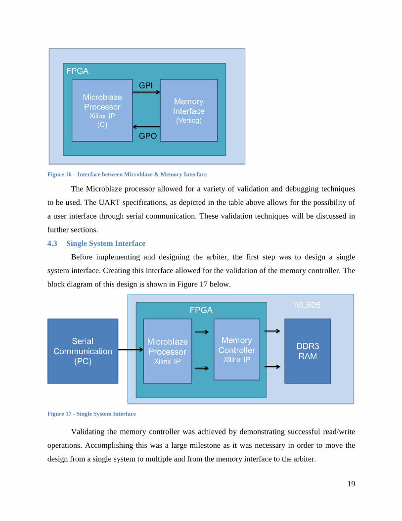
Figure 16 – Interface between Microblaze & Memory Interface ................................................. 19
Figure 17 - Single System Interface.............................................................................................. 19
Figure 18 - Two System Interface w/ DDR3 ................................................................................ 20
Figure 19 - Expanded Block Diagram Showing Arbiter Block .................................................... 21
Figure 20 - Traffic Generator Top Level Block ............................................................................ 21
Figure 21 - State Diagram for Traffic Generator .......................................................................... 22
Figure 22 - FIFO Top Level Block ............................................................................................... 23
Page 11
v
Figure 23 - Fixed Priority Arbiter Top Level Block ..................................................................... 24
Figure 24 - Flow Chart for Fixed Priority Arbiter ........................................................................ 25
Figure 25: Flow chart for timeout logic ........................................................................................ 26
Figure 26: Write Path Simulation ................................................................................................. 28
Figure 27: Read Path Simulation (Enable Sequence) ................................................................... 28
Figure 28: Read Path Simulation (app_rd_data_valid) ................................................................. 29
Figure 29: Arbitration of System 1 over System 2 ....................................................................... 29
Figure 30: Low Priority System Grant (No starvation) ................................................................ 30
Figure 31: Timeout (2 cycles) System 2 is Granted over System 1 .............................................. 30
Figure 32: Three Write Commands through to Memory Controller ............................................. 31
Figure 33 - Single System/Memory Test ...................................................................................... 32
Figure 34 - Pre-Enable .................................................................................................................. 33
Figure 35 - Traffic Enable, Starvation .......................................................................................... 34
Figure 36 - Timeout Validation .................................................................................................... 35
Figure 37: Timing for Back to Back Write Commands [14] ........................................................ 37
Page 12
1
1 Introduction
Fast volatile memory is designed for use with one system. In order for multiple systems
to use the same memory, there must be some facilitation between the two systems and the
memory in order to avoid errors and data corruption. This can be very helpful for many different
applications to cut costs, save space, reduce complexity or more. Teradyne has requested the
design of an arbiter so that it can possibly be used to aid in a variety of testing applications. For
example, if one of their test units has any interaction with a memory unit, another system must
validate that interaction and thus also access that unit. One method to facilitate the two systems
communication is by implementing an arbiter.
An arbiter is the term used for an object that facilitates or arbitrates interaction between
two distinct blocks [1]. The arbiter follows a set of rules to pass the communication between the
two blocks. While arbiters can be used in a variety of applications, in this case it is implemented
on a Field Programmable Gate Array (FPGA) between some systems and a single memory
module where the systems are distinct. A consideration that a memory arbiter needs to take is
how it determines which system is granted access in order to fairly share access.
This project set out to design and create the arbiter using an HDL (hardware description
language) (Verilog), and validate it using an ML605 evaluation board. There are a few goals that
were essential for the progression and completion of this project. First, sending read/write
commands to memory was done with no arbiter so that there is a functioning interface to
memory. Second, the arbiter rules were created and the arbiter was designed. Thirdly, a
validation process for the arbiter was designed and carried out. These three goals were necessary
to create a useful, functional memory arbiter.
Page 13
2
2 Background
Today random access memory (RAM) is widely used in computers and other electronics as
a way to access and store data. This type of computer memory can be accessed randomly and
without the need to access preceding or following data addresses. However, RAM is volatile
memory and will only retain data as long as power is on. Once the system loses power, it loses
any data stored in memory. RAM has evolved over time as engineers try to achieve better speed
and efficiency [2].
2.1 Static Random Access Memory (SRAM)
Static Random Access Memory (SRAM) is a variation of RAM. SRAM is designed to fill
two needs: provide a direct interface to CPUs at speeds unattainable by DRAMs (will be covered
later) and replace DRAMs in systems that require very low power consumption [3]. SRAM
performs very well in low power applications due to the nature of the device. SRAM cells are
comprised of six MOSFETs. Below in Figure 1 shows this.
Figure 1 - SRAM Six Transistors [4]
Four transistors act as cross coupled inverters holding the bit information, while the
remaining transistors control access to data during read/write operations. SRAM is preferred in
portable equipment because of its low power capability and because it does not require a refresh
cycle due to the absence of capacitors in its design. Although SRAM is still volatile, data will not
leak away. This type of RAM is not used in more applications simply due to its price [5].
Page 14
3
2.2 Dynamic Random Access Memory (DRAM)
The other major category of RAM is Dynamic Random Access Memory (DRAM). As with
SRAM, DRAM fundamentally holds onto the information of individual bits, but unlike SRAM, it
is designed with capacitors along with transistors, shown below in Figure 2.
Figure 2 - DRAM Schematic [6]
The number of transistors is reduced to one in DRAM making it fundamentally simpler than
SRAM. However since capacitors lose their charge over time, a refresh is needed to maintain
stored data, which increases power usage due to the voltage of the capacitors The inability to
maintain information without a refresh is why DRAM is considered dynamic as opposed to its
“static” counterpart [7].
DRAM is used for its simplicity and its lower cost, however at the price of performance and
efficiency. Engineers have been pushing the technology forward to improve its performance.
When analyzing RAM it is important to look at bandwidth and latency. Bandwidth is the amount
of data transferred per second, and latency is the time between sending an address to memory
and receiving the data back on the data bus [8].These improvements are seen in various iterations
of DRAM.
2.2.1 Synchronous DRAM (SDRAM)
SDRAM is synchronized with the system’s clock. This interface waits for a clock signal
before responding to inputs, resulting in data being available at every clock cycle. Asynchronous
Page 15
4
RAM attempts to respond to commands as soon as possible. To increase efficiency, memory is
divided into several banks, enabling simultaneous processing of memory access commands. An
address is comprised of bank, row, and column information [7].
2.2.2 Double Data Rate 1 (DDR1) SDRAM
To increase bandwidth, double data rate is introduced in DDR1 memory. Without having to
increase clock speed, DDR1 transfers data on both the rising and falling edge of the clock.
Additional power efficiency is achieved by reducing the supply voltage from 3.3V to 2.5V.
A 2n-prefetch architecture is introduced which allows 2 bits of data to be transferred to the
queue in two separate pipelines. Without changing the clock, bandwidth is doubled with this
interface [7].
2.2.3 DDR2 SDRAM
DDR2 makes further improvements upon earlier variations of SDRAM. Operation
voltage lowered to 1.8V, decreasing total power consumption. Additionally, a 4n-prefetch buffer
is added. Improving upon the previous 2 bits, 4 bits are now able to be transferred per clock
cycle from the memory array to the data bus. DDR2 data rates are up to eight times faster than
the original SDRAM [7].
2.2.4 DDR3 SDRAM
As with previous generations, DDR3 decreases power consumption and increases bandwidth.
DDR3 uses a 1.5V power supply as opposed to the 1.8V power supply used in DDR2 and its
bandwidth can be up to twice that of DDR2 [8]. DDR3 has eight banks, which allows more
efficient bank access than in previous interfaces with four. Additionally, the prefetch buffer is
increased to 8 bits wide, resulting in an 8n interface [7].
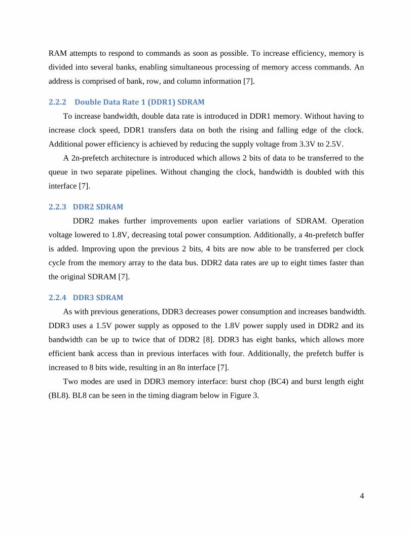
Two modes are used in DDR3 memory interface: burst chop (BC4) and burst length eight
(BL8). BL8 can be seen in the timing diagram below in Figure 3.
Page 16
5
Figure 3 - DDR3 Timing Diagram [9]
BL8 allows for addressing to occur once every eight data packets are sent, because consecutive
memory addresses are used. BC4 allows bursts of four by treating data as though half of it is
masked. Of the two options, BL8 is more widely used [8].
2.3 Arbitration
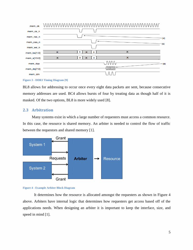
Many systems exist in which a large number of requesters must access a common resource.
In this case, the resource is shared memory. An arbiter is needed to control the flow of traffic
between the requestors and shared memory [1].
Figure 4 - Example Arbiter Block Diagram
It determines how the resource is allocated amongst the requesters as shown in Figure 4
above. Arbiters have internal logic that determines how requesters get access based off of the
applications needs. When designing an arbiter it is important to keep the interface, size, and
speed in mind [1].
Page 17
6
2.3.1 Arbitration Schemes
Many arbitration schemes already exist. These include round robin, first in first out,
priority, and dynamic priority. The section below describes some of the schemes that we
researched before the design of our own arbiter.
2.3.1.1 Round robin
In round robin, each system receives a specific amount of time to access memory and the
systems cycle through in a pre-defined order [1]. A timing diagram of this technique can be seen
below. The ready signal seen at the top of the timing diagram in Figure 5 is a depiction of the
memory cycles, with each grant occurring at the positive edge of each cycle.
Figure 5 - Round Robin Timing Diagram
In round robin systems are granted access entirely based off order rather than requests.
This makes it an unfavorable option for arbiter designs stressing efficiency as systems may be
granted access when not requesting, which results in arbiter idle time.
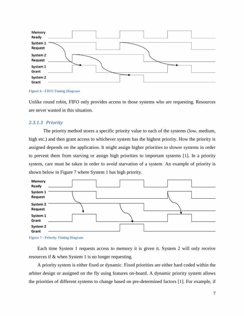
2.3.1.2 First In First Out
In first in first out whichever system asks for the memory first receives it. The arbiter
keeps track of which system asserted its ready signal first and then gives it to that system [1]. An
example of FIFO timing can be seen below in Figure 6. System 1 requests access first and
receives initial grant. System 2 then requests access to memory and is then shown to be given
access after System 1 de-asserts its request.
Memory Ready
System 1 Request
System 2 Request
System 1 Grant
System 2 Grant
Page 18
7
Figure 6 - FIFO Timing Diagram
Unlike round robin, FIFO only provides access to those systems who are requesting. Resources
are never wasted in this situation.
2.3.1.3 Priority
The priority method stores a specific priority value to each of the systems (low, medium,
high etc.) and then grant access to whichever system has the highest priority. How the priority is
assigned depends on the application. It might assign higher priorities to slower systems in order
to prevent them from starving or assign high priorities to important systems [1]. In a priority
system, care must be taken in order to avoid starvation of a system. An example of priority is
shown below in Figure 7 where System 1 has high priority.
Figure 7 - Priority Timing Diagram
Each time System 1 requests access to memory it is given it. System 2 will only receive
resources if & when System 1 is no longer requesting.
A priority system is either fixed or dynamic. Fixed priorities are either hard coded within the
arbiter design or assigned on the fly using features on-board. A dynamic priority system allows
the priorities of different systems to change based on pre-determined factors [1]. For example, if
Memory Ready
System 1 Request
System 2 Request
System 1 Grant
System 2 Grant
Page 19
8
one system was accessing memory more often than another system, the higher traffic system
could gain higher priority. Another example would be to change priority based on how long a
system goes without accessing memory. The scheme chosen depends on the requirements of the
system.
Page 20
9
3 Methodology
This section describes the methods used for completion of the project. The hardware and
tools that were used in the project are discussed, as well as tools used for design and validation.
Following that discussion, the project’s requirements that were decided upon at the start of the
project are described. Finally, the methods of validation for the project are described.
3.1 Hardware
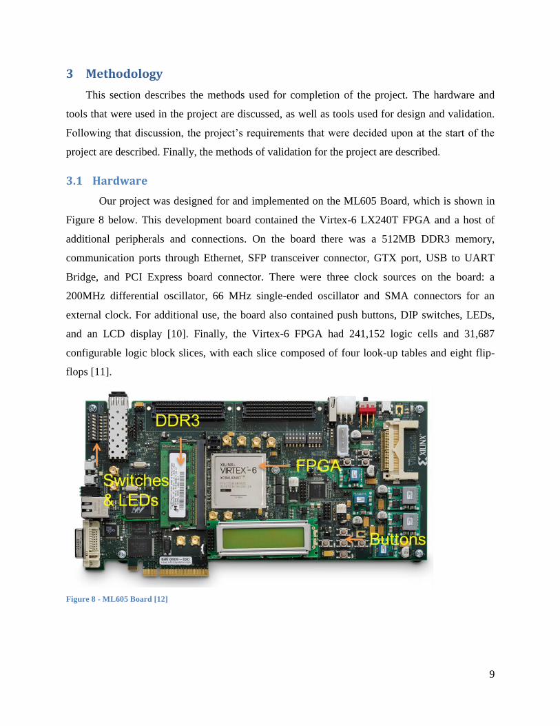
Our project was designed for and implemented on the ML605 Board, which is shown in
Figure 8 below. This development board contained the Virtex-6 LX240T FPGA and a host of
additional peripherals and connections. On the board there was a 512MB DDR3 memory,
communication ports through Ethernet, SFP transceiver connector, GTX port, USB to UART
Bridge, and PCI Express board connector. There were three clock sources on the board: a
200MHz differential oscillator, 66 MHz single-ended oscillator and SMA connectors for an
external clock. For additional use, the board also contained push buttons, DIP switches, LEDs,
and an LCD display [10]. Finally, the Virtex-6 FPGA had 241,152 logic cells and 31,687
configurable logic block slices, with each slice composed of four look-up tables and eight flip-
flops [11].
Figure 8 - ML605 Board [12]
Page 21
10
3.1.1 Onboard DDR3 Memory
As mentioned above the ML605 board came with a Micron 512 MB DDR3 Memory
SODIMM. DDR3 is the third generation of SDRAM. It provides two burst modes for both
Reads/Writes burst chop and burst length eight. The first mode is burst chop (BC4), which
allows bursts of four by treating data as though half of it is masked. The second method, burst
length eight (BL8), is the primary burst mode. This is done with a pre-fetch of 8n, which means
that during a read operation, eight data-words can be read with one address request [7].
3.2 Project Requirements
During our design meetings with Teradyne we decided upon many project requirements.
These were the guidelines we followed during the design of the arbiter. Below the requirements
are described in more detail.
3.2.1 Multiple Systems
The arbiter was designed to allow multiple systems to access the shared DDR3 memory.
It was able to handle two separate systems with the prospect of adding more. Creating systems
that generate read and write commands similar to what might be generated by real systems was
the method used to validate the functionality of our arbiter design. These systems were
represented by generating traffic within the FPGA.
3.2.2 Programmable Priority
The arbiter exhibited on-the-fly priority. This allows the arbiter to be able to dynamically
change which system receives priority without having to modify the Verilog source code. This
can be done utilizing module I/O ports. The arbiter should have a signal that can control which
system has priority.
3.3 Development Tools
For our design we used the Xilinx Integrated Software Environment (ISE). Here we
created modules, test benches, and generate other necessary cores for our project. Our main
method of programming was the Verilog HDL. Additionally, Xilinx IP Cores were generated to
assist in the development and testing of various modules.
Page 22
11
3.3.1 Xilinx Integrated Software Environment
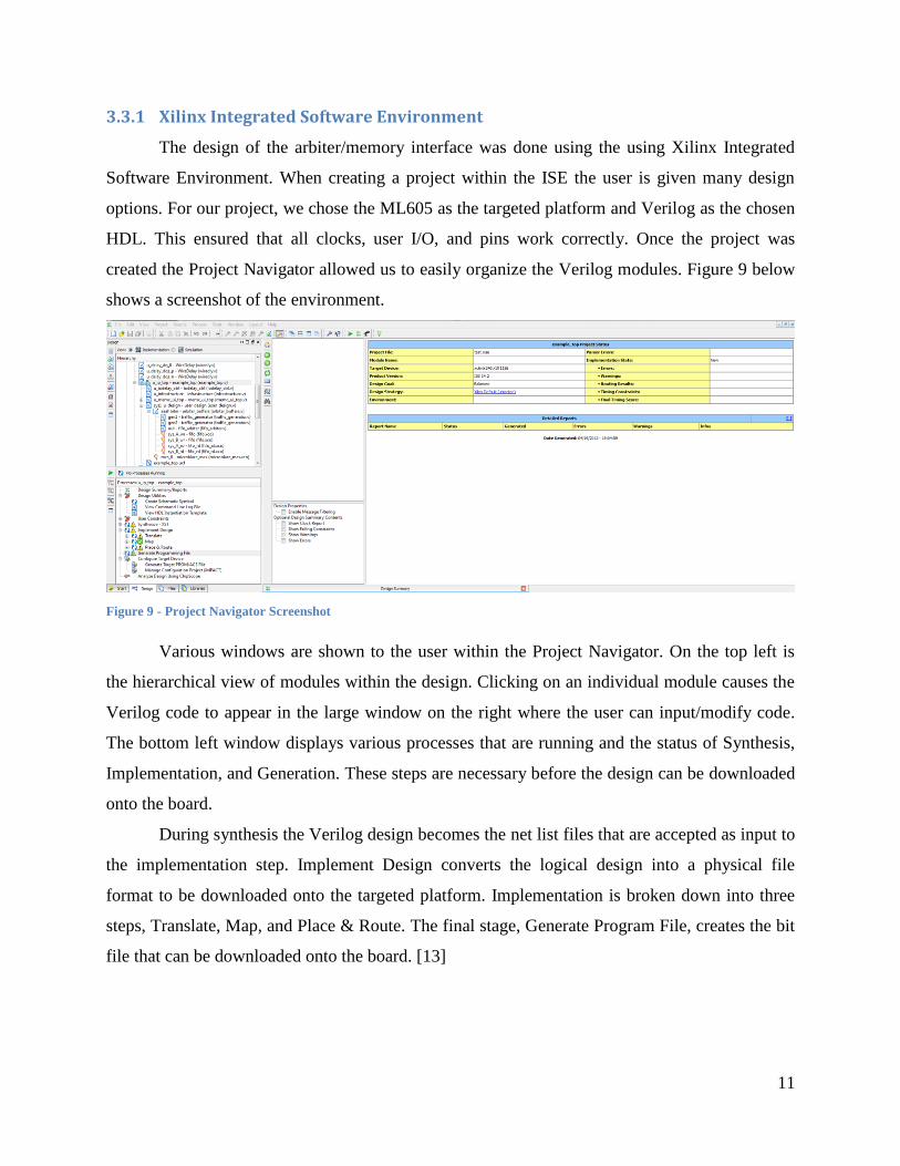
The design of the arbiter/memory interface was done using the using Xilinx Integrated
Software Environment. When creating a project within the ISE the user is given many design
options. For our project, we chose the ML605 as the targeted platform and Verilog as the chosen
HDL. This ensured that all clocks, user I/O, and pins work correctly. Once the project was
created the Project Navigator allowed us to easily organize the Verilog modules. Figure 9 below
shows a screenshot of the environment.
Figure 9 - Project Navigator Screenshot
Various windows are shown to the user within the Project Navigator. On the top left is
the hierarchical view of modules within the design. Clicking on an individual module causes the
Verilog code to appear in the large window on the right where the user can input/modify code.
The bottom left window displays various processes that are running and the status of Synthesis,
Implementation, and Generation. These steps are necessary before the design can be downloaded
onto the board.
During synthesis the Verilog design becomes the net list files that are accepted as input to
the implementation step. Implement Design converts the logical design into a physical file
format to be downloaded onto the targeted platform. Implementation is broken down into three
steps, Translate, Map, and Place & Route. The final stage, Generate Program File, creates the bit
file that can be downloaded onto the board. [13]
Page 23
12
3.3.2 Xilinx Core Generator
The core generator became a very useful tool used for design, implementation, and
verification. Xilinx allows users to choose from a variety of IP Cores that they create to simplify
design. Figure 10 below shows the various IP Cores that can be generated through Xilinx.
Figure 10 - Xilinx IP Cores
Highlighted in the figure above are the cores used in our design. The Xilinx Memory
Interface Generator (MIG) was the most important. This created a memory controller with a
much simpler to design user interface. Additionally, we were able to generate a Microblaze Soft
core Processor used for hardware validation and also various FIFOs dedicated for queuing
commands. Each of these cores will be discussed in greater detail within the Design &
Implementation Chapter.
3.3.3 Software Development Kit
The Software Development Kit was used in the design of the Microblaze soft core
processor mentioned in the previous section. This gave us an easy development environment to
Page 24
13
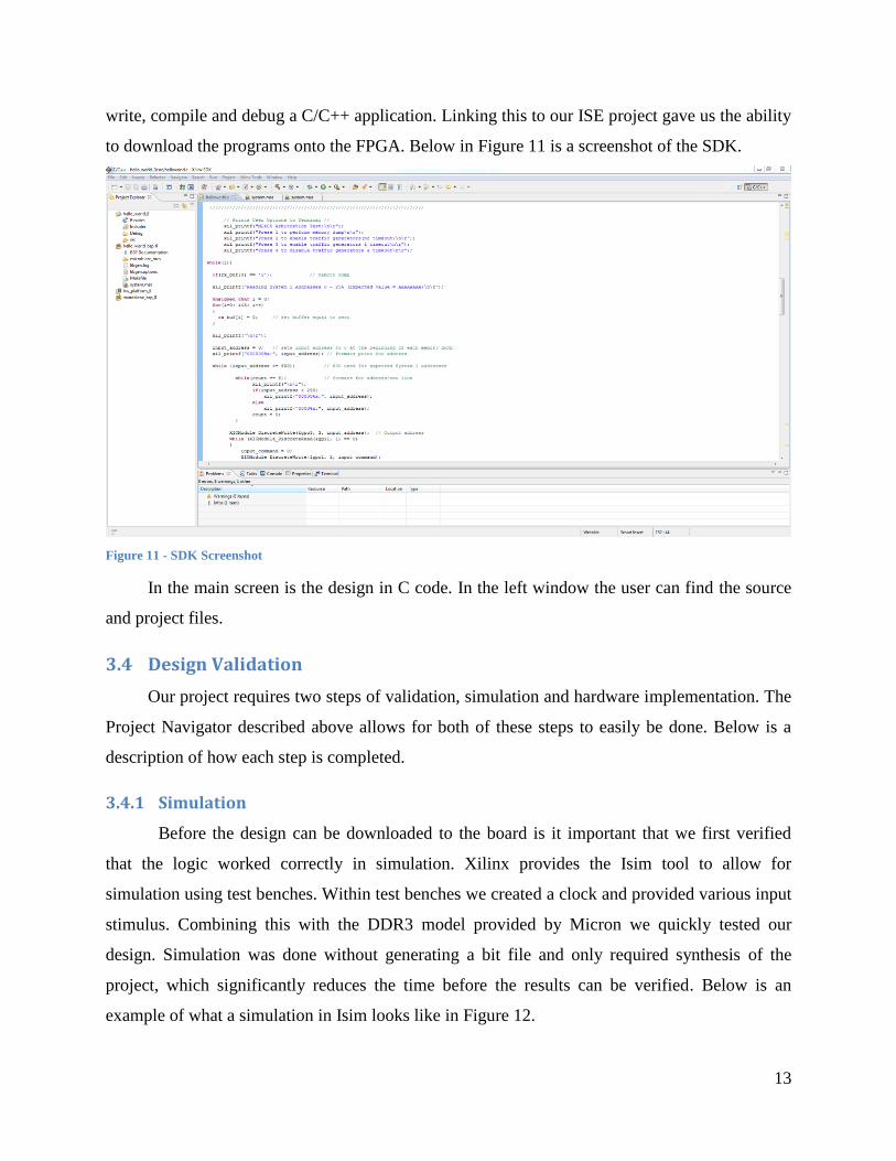
write, compile and debug a C/C++ application. Linking this to our ISE project gave us the ability
to download the programs onto the FPGA. Below in Figure 11 is a screenshot of the SDK.
Figure 11 - SDK Screenshot
In the main screen is the design in C code. In the left window the user can find the source
and project files.
3.4 Design Validation
Our project requires two steps of validation, simulation and hardware implementation. The
Project Navigator described above allows for both of these steps to easily be done. Below is a
description of how each step is completed.
3.4.1 Simulation
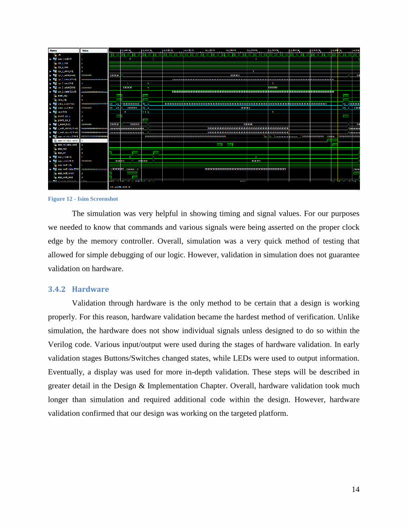
Before the design can be downloaded to the board is it important that we first verified
that the logic worked correctly in simulation. Xilinx provides the Isim tool to allow for
simulation using test benches. Within test benches we created a clock and provided various input
stimulus. Combining this with the DDR3 model provided by Micron we quickly tested our
design. Simulation was done without generating a bit file and only required synthesis of the
project, which significantly reduces the time before the results can be verified. Below is an
example of what a simulation in Isim looks like in Figure 12.
Page 25
14
Figure 12 - Isim Screenshot
The simulation was very helpful in showing timing and signal values. For our purposes
we needed to know that commands and various signals were being asserted on the proper clock
edge by the memory controller. Overall, simulation was a very quick method of testing that
allowed for simple debugging of our logic. However, validation in simulation does not guarantee
validation on hardware.
3.4.2 Hardware
Validation through hardware is the only method to be certain that a design is working
properly. For this reason, hardware validation became the hardest method of verification. Unlike
simulation, the hardware does not show individual signals unless designed to do so within the
Verilog code. Various input/output were used during the stages of hardware validation. In early
validation stages Buttons/Switches changed states, while LEDs were used to output information.
Eventually, a display was used for more in-depth validation. These steps will be described in
greater detail in the Design & Implementation Chapter. Overall, hardware validation took much
longer than simulation and required additional code within the design. However, hardware
validation confirmed that our design was working on the targeted platform.
Page 26
15
4 Design & Implementation
This section explains the design of the memory interface, arbiter and surrounding
modules. Each module relevant to the function of the arbiter is described in detail.
4.1 Memory Interface
The memory controller that was required to handle the complexity of DDR3 usage has
specific signals that are provided to the user for control of the controller itself. These signals
have very specific timings that are necessary to ensure proper data transfer to the DDR3 memory.
Each type of command requires a different sequence of signal changes. Xilinx's documentation
for their IP was important to understand exactly how to interface with the memory controller.
This section will examine the necessary execution sequence on the signals of the memory
controller and then describe the solution that was used for it.
Firstly, the write path described in the memory interface user guide [14] requires the use of
a single 256bit data line and some control signals. The command and address signals must be set
and held until the memory is ready, while simultaneously placing the data one the data line. This
is shown in Figure 13, a timing diagram from the user guide. It should be noted that this is burst
length 8 accesses where the DDR3 has addresses widths of 64 bits.
Figure 13: Write Timing Diagram [14]
Page 27
16
It is important that the app_rdy and app_wdf_rdy signals were monitored to ensure that
the command is ready to be accepted and the memory controller was not executing a refresh or
busy.
The read path required a similar enable sequence without the need to place anything on
the data line. The timing diagram is shown in Figure 14. As can be seen, the enable sequence
occurs and then after an undefined period of time the data appears on a separate data line which
is delineated with the app_rd_data_valid signal.
Figure 14: Read Timing Diagram [14]
To meet these specifications in timing for these signals, a state machine was created that
uses the signals that must be polled as inputs and then controls the sequences that must change.
A state diagram is shown in Figure 15 which shows how each state can change between each
other. The app_rdy, wdf_rdy and similar signals triggered the changes between some of the states.
Page 28
17
Figure 15: State Diagram for Memory Interface
The system begins in the idle state, where the state machine waits for a command. Once a
command is sent, it checks which type of command it is and goes to the appropriate state
read_wait_en or write_data. The first read state is where the enable sequence begins and the
address is latched into the memory controller. This enable sequence must be held until app_rdy
is asserted. Once that occurs, the next state read_wait_data waits for the app_rd_data_valid
signal to assert itself so that the data can be saved.
If a write command was detected, the data and address are latched in the first state. The
next state begins the enable sequence and puts the second half of the data on the data line. Since
the second half is the end data this state also asserts app_wdf_end to tell the memory controller it
is the last data that must be written. The next state is simply a state that waits until both the
app_wdf_rdy and app_rdy signals are asserted so that the data does not have to be held, and the
enable sequence does not need to be held.
This memory interface was crucial to use when accessing memory, and was the first
module that was created in order to complete this project.
Idle
read_wait_en
read_wait_data
read_d1
write_data
write_d1
write_d2
cmd_rdy && cmd = 0
app_wdf_rdy = 1 &&
app_rdy = 1
cmd_rdy && cmd = 1
app_rdy = 1
app_rd_data_valid = 1
Page 29
18
4.2 Microblaze Processor
As mentioned in the methodology, the Microblaze is a soft processor core designed for
Xilinx FPGAs. As other IPs, it is completely designed and provided by Xilinx. When adding a
Microblaze to a project the user is presented with many design options. These include, clock
speed, UART, General Purpose Outputs (GPO), General Purpose Inputs (GPI), Fixed Interval
Timing, Programmable Interval Timing, and Interrupts. For the purposes of this project only the
clock, UART, and GPO/I need to be used. The table below shows the characteristics of the
generated processor.
Clock Located on ML605 66Mhz
Memory Size Created within Virtex6 64KB
UART Receiver/Transmitter 9600 Baud Rate
GPO Up to 4 32 Bits
GPI Up to 4 32 Bits
Initially, the GPO/I were the most important factors to worry about regarding the
Microblaze. These data determine how information was transferred between the rest of the
FPGA and the processor. The GPOs output commands, data, and addresses from the processor.
Similarly, the processor receives GPIs for read data and addresses. The remaining data lines were
used for various debugging purposoes.
The Microblaze processor was generated within the FPGA. It is important to note that it
is not an external processor. By creating a workspace within the SDK we were able to use C
programming to code the soft core processor. This allowed for computations and display to be
done much simpler. A block diagram of the interface between the Microblaze and the memory
interface module is shown below in Figure 16.
Page 30
19
Figure 16 – Interface between Microblaze & Memory Interface
The Microblaze processor allowed for a variety of validation and debugging techniques
to be used. The UART specifications, as depicted in the table above allows for the possibility of
a user interface through serial communication. These validation techniques will be discussed in
further sections.
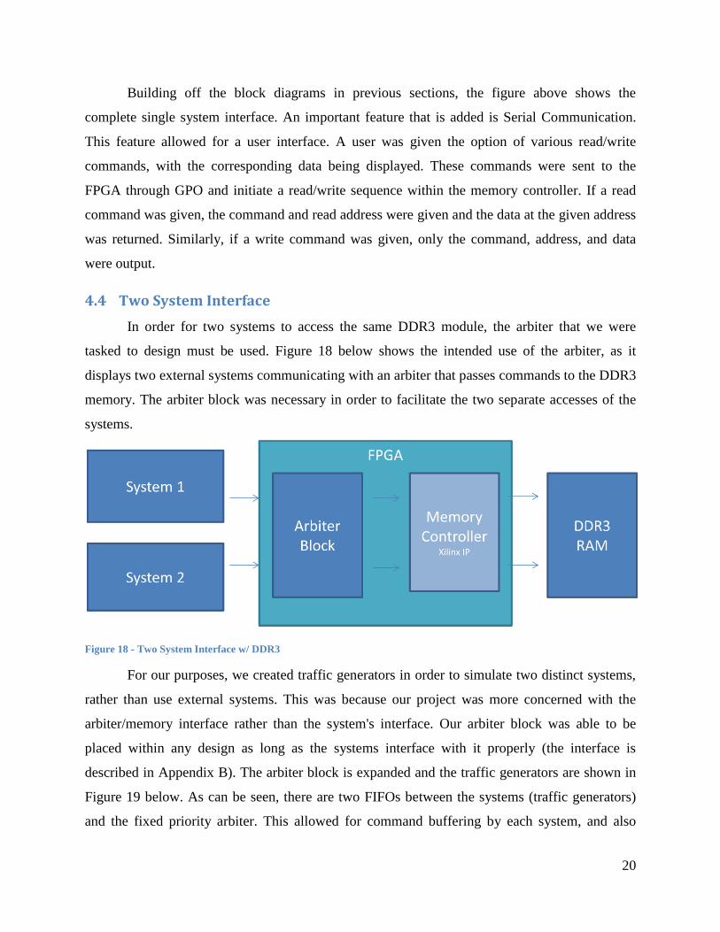
4.3 Single System Interface
Before implementing and designing the arbiter, the first step was to design a single
system interface. Creating this interface allowed for the validation of the memory controller. The
block diagram of this design is shown in Figure 17 below.
Figure 17 - Single System Interface
Validating the memory controller was achieved by demonstrating successful read/write
operations. Accomplishing this was a large milestone as it was necessary in order to move the
design from a single system to multiple and from the memory interface to the arbiter.
Page 31
20
Building off the block diagrams in previous sections, the figure above shows the
complete single system interface. An important feature that is added is Serial Communication.
This feature allowed for a user interface. A user was given the option of various read/write
commands, with the corresponding data being displayed. These commands were sent to the
FPGA through GPO and initiate a read/write sequence within the memory controller. If a read
command was given, the command and read address were given and the data at the given address
was returned. Similarly, if a write command was given, only the command, address, and data
were output.
4.4 Two System Interface
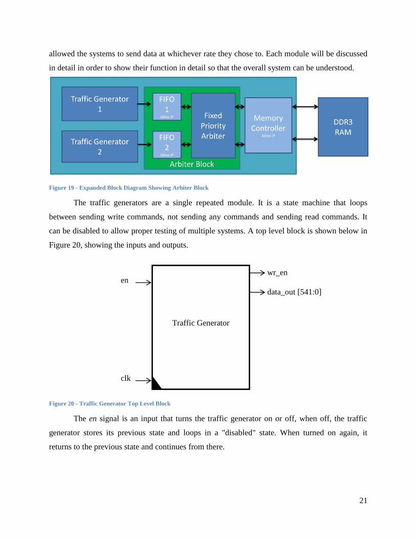
In order for two systems to access the same DDR3 module, the arbiter that we were
tasked to design must be used. Figure 18 below shows the intended use of the arbiter, as it
displays two external systems communicating with an arbiter that passes commands to the DDR3
memory. The arbiter block was necessary in order to facilitate the two separate accesses of the
systems.
Figure 18 - Two System Interface w/ DDR3
For our purposes, we created traffic generators in order to simulate two distinct systems,
rather than use external systems. This was because our project was more concerned with the
arbiter/memory interface rather than the system's interface. Our arbiter block was able to be
placed within any design as long as the systems interface with it properly (the interface is
described in Appendix B). The arbiter block is expanded and the traffic generators are shown in
Figure 19 below. As can be seen, there are two FIFOs between the systems (traffic generators)
and the fixed priority arbiter. This allowed for command buffering by each system, and also
Page 32
21
allowed the systems to send data at whichever rate they chose to. Each module will be discussed
in detail in order to show their function in detail so that the overall system can be understood.
Figure 19 - Expanded Block Diagram Showing Arbiter Block
The traffic generators are a single repeated module. It is a state machine that loops
between sending write commands, not sending any commands and sending read commands. It
can be disabled to allow proper testing of multiple systems. A top level block is shown below in
Figure 20, showing the inputs and outputs.
Figure 20 - Traffic Generator Top Level Block
The en signal is an input that turns the traffic generator on or off, when off, the traffic
generator stores its previous state and loops in a "disabled" state. When turned on again, it
returns to the previous state and continues from there.
Traffic Generator
wr_en
data_out [541:0]
en
clk
Page 33
22
The wr_en signal is an output that tells the FIFO buffer that there is valid data on the
output. This is necessary for the FIFO buffer in the following block to acknowledge the traffic
generator.
The data_out contains the command, the address and for a write command, the data to be
written. {data, addr, cmd}. This is written into the FIFO buffers when wr_en is asserted and then
broken down into individual data, address and command signals before being passed to the
arbiter.
There are also 3 parameters that are useful in testing different situations of the arbiter.
There is a parameter that controls the data that is sent for write commands, one that controls the
amount of accesses that are sent per state and one that controls the starting address (so that
different systems can write to different addresses).
Now that the top level of the traffic generator is described, the state diagram is shown in
Figure 21 below. The transitions between each state occur after a specific amount of accesses
have been written to the FIFOs which are hard coded through parameters.
Figure 21 - State Diagram for Traffic Generator
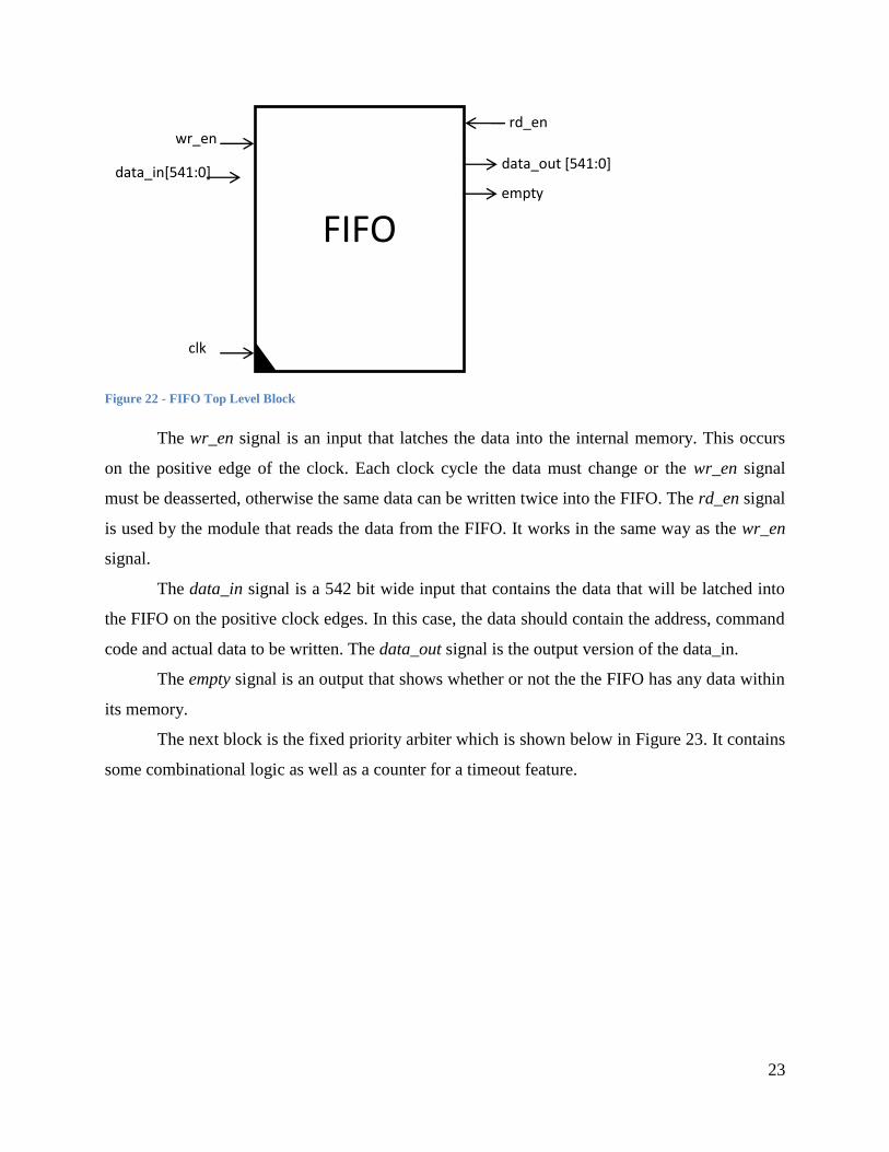
The next module in the design are the FIFOs, which are standard cores generated by the
Xilinx. The top level block is still shown in Figure 22. Data is queued into the FIFO's memory
and de-queued in order.
Start
Write
Idle
Read
Page 34
23
Figure 22 - FIFO Top Level Block
The wr_en signal is an input that latches the data into the internal memory. This occurs
on the positive edge of the clock. Each clock cycle the data must change or the wr_en signal
must be deasserted, otherwise the same data can be written twice into the FIFO. The rd_en signal
is used by the module that reads the data from the FIFO. It works in the same way as the wr_en
signal.
The data_in signal is a 542 bit wide input that contains the data that will be latched into
the FIFO on the positive clock edges. In this case, the data should contain the address, command
code and actual data to be written. The data_out signal is the output version of the data_in.
The empty signal is an output that shows whether or not the the FIFO has any data within
its memory.
The next block is the fixed priority arbiter which is shown below in Figure 23. It contains
some combinational logic as well as a counter for a timeout feature.
FIFO
rd_en
data_out [541:0]
wr_en
clk
data_in[541:0]
empty
Page 35
24
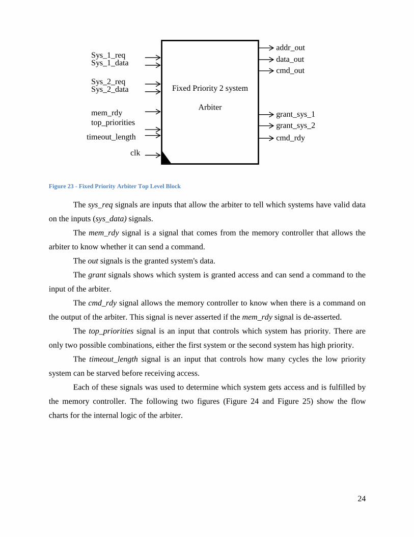
Figure 23 - Fixed Priority Arbiter Top Level Block
The sys_req signals are inputs that allow the arbiter to tell which systems have valid data
on the inputs (sys_data) signals.
The mem_rdy signal is a signal that comes from the memory controller that allows the
arbiter to know whether it can send a command.
The out signals is the granted system's data.
The grant signals shows which system is granted access and can send a command to the
input of the arbiter.
The cmd_rdy signal allows the memory controller to know when there is a command on
the output of the arbiter. This signal is never asserted if the mem_rdy signal is de-asserted.
The top_priorities signal is an input that controls which system has priority. There are
only two possible combinations, either the first system or the second system has high priority.
The timeout_length signal is an input that controls how many cycles the low priority
system can be starved before receiving access.
Each of these signals was used to determine which system gets access and is fulfilled by
the memory controller. The following two figures (Figure 24 and Figure 25) show the flow
charts for the internal logic of the arbiter.
Fixed Priority 2 system
Arbiter
addr_out
data_out Sys_1_req
clk
Sys_1_data
Sys_2_req Sys_2_data
cmd_out
grant_sys_1
grant_sys_2
mem_rdy
top_priorities
timeout_length cmd_rdy
Page 36
25
Figure 24 - Flow Chart for Fixed Priority Arbiter
Grant_sys_2
cmd_rdy and pass
sys_2_data to the
output
Is mem_rdy?
System 2 has high
priority
no
Don’t grant
either system
Sys_1_req?
Grant_sys_1
cmd_rdy and pass
sys_1_data to the
output
Sys_2_req?
Grant_sys_2
cmd_rdy and pass
sys_2_data to the
output
Grant both systems,
deassert cmd_rdy
yes
Check Priorities System 1 has high
priority
Sys_2_req?
Sys_1_req?
Grant_sys_1
cmd_rdy and pass
sys_1_data to the
output
Grant both systems,
deassert cmd_rdy
no
no
no
no
yes
yes
yes
Page 37
26
Figure 25: Flow chart for timeout logic
The interaction of each module described above can be seen in Appendix A which goes on to
connect with the memory controller.
Negative
edge of
mem_rdy
Check Priorities
System 1 has high
priority
System 2 has high
priority
Is system 2 starved?
Is system 1 starved?
Reset timeout
counter
Reset timeout
counter
Increment
counter Increment
counter
Timeout occured?
Invert real
priorities Reset to
programmed
priorities
Page 38
27
5 Arbiter Validation & Results
After designing the arbiter, its function was tested by using the two traffic generators as
distinct systems. This was carried out in simulation and in hardware on-board the ML605.
Simulation was carried out in the ISim tool using a Micron DDR3 model provided by the
memory interface generator. By examining the relevant signals it was possible to verify that the
arbiter was functioning with the provided model as well as provided significant help in
debugging issues. On-board, a Microblaze processor monitored and performed memory checks
on the addresses affected by the traffic generators. The results that were sent to the Microblaze
were then printed on a PC terminal (TeraTerm) through serial communication. Both of these
methods were essential in confirming that the arbiter was functional.
5.1 Validation in Simulation
This section describes the verification phases in simulation. Simulation allowed us to look
directly at individual signals within the design and check their function. This was the tool to use
for debugging, as it was the fastest way to check whether something was functioning as it should.
It also allowed us to verify every single module individually, then the interaction between them
and finally the overall design, which was not as feasible on hardware as some modules do not
have any visible I/O to the hardware.
5.1.1 Single-System Interface
The single system interface was the most difficult to debug, as it was very reliant on the
DDR3 memory and memory controller IP core which were both very complex pieces. For this,
we used a DDR3 memory model provided by Micron. The DDR3 model allowed us to see
whether or not commands were being carried out, and whether or not they returned the proper
data. As seen in a previous section, the memory controller requires very strict timings on the
important signals in order to properly carry out the commands. Each command has a different
protocol, so looking at the timing that we generate for each command is important. Recall that
the interface to the memory controller used a state machine to generate the proper timing.
Firstly, the write path is investigated to ensure that writes were being carried out as they
should. For the write path it is important that the app_rdy and app_wdf_rdy signals are adhered
to, but also that sending the data through to the memory controller occurs within 2 clock cycles
of the enable sequence. Figure 26 shows the simulation results from with the relevant signals
Page 39
28
being changed as expected. It should be noted that the entire sequence for a write path only takes
2 clock cycles (10 ns). Also, the data “aaaa…” is being written to address “8”, where we will
perform a read command to check the data within that address.
Figure 26: Write Path Simulation
Secondly, the read path was investigated to ensure that data that is written can actually be
read back. The read path was simpler than the write path, as when the enable sequence occur, it
was a simple matter of polling the app_rd_data_valid signal until the data becomes available.
Figure 26 displays the enable sequence, and shows app_rd_data_valid not asserting, after a few
clock cycles Figure 27 shows the data being retrieved when app_rd_data_valid is asserted.
Figure 27: Read Path Simulation (Enable Sequence)
The read command in these figures was being performed on address 8, which was written
to earlier in the simulation. As seen in Figure 28, the data was correct when valid which was
exactly what we expected. This time period was exactly when the data should be sent back to the
system that requested this command.
Page 40
29
Figure 28: Read Path Simulation (app_rd_data_valid)
The signals in these simulations are working correctly, and are ready to be tested on
hardware. Section 5.2.1 describes the hardware validation of the single system interface.
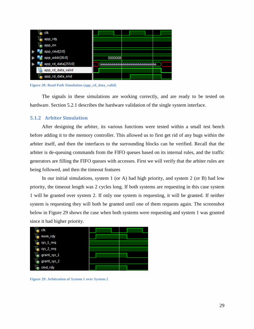
5.1.2 Arbiter Simulation
After designing the arbiter, its various functions were tested within a small test bench
before adding it to the memory controller. This allowed us to first get rid of any bugs within the
arbiter itself, and then the interfaces to the surrounding blocks can be verified. Recall that the
arbiter is de-queuing commands from the FIFO queues based on its internal rules, and the traffic
generators are filling the FIFO queues with accesses. First we will verify that the arbiter rules are
being followed, and then the timeout features
In our initial simulations, system 1 (or A) had high priority, and system 2 (or B) had low
priority, the timeout length was 2 cycles long. If both systems are requesting in this case system
1 will be granted over system 2. If only one system is requesting, it will be granted. If neither
system is requesting they will both be granted until one of them requests again. The screenshot
below in Figure 29 shows the case when both systems were requesting and system 1 was granted
since it had higher priority.
Figure 29: Arbitration of System 1 over System 2
Page 41
30
If system 1 is not requesting, system 2 should be granted. This is shown in Figure 30
below, as system 2 is granted when system 1 is never requesting. This shows the zero idle time
within this arbiter design.
Figure 30: Low Priority System Grant (No starvation)
With a timeout length of two cycles, system 2 will be granted after system 1 is granted
twice in a row. This is shown below in Figure 31 where system 2 is granted after 2 cycles even
though system 1 is also requesting.
Figure 31: Timeout (2 cycles) System 2 is Granted over System 1
Furthermore, it was important to verify whether or not the commands get carried out by
the memory controller after being granted and passed through the arbiter. Below in Figure 32,
three cycles are shown, and the memory controller timing that was discussed in the previous
section is properly taking the data from the arbiter and carrying out the command to memory.
The read commands from the traffic generators were also verified in this manner.
Page 42
31
Figure 32: Three Write Commands through to Memory Controller
5.2 Hardware Validation
This section serves to discuss the multiple steps of hardware validation. As simulations
were verified, hardware tests followed. Three distinct tests were done to verify functionality of
the memory controller and the arbiter. Single system, memory, and arbiter tests were created.
5.2.1 Single-System Interface
As described above a single system was created to test the function of the memory
controller. The serial interface acts as an individual system, but is quite slow (frequency of
commands) when compared to realistic systems. It sends one command at a time, taking
commands from a user and displaying the results on the screen. Additionally, it was found that
the single system only validates the memory controller on the small scale, meaning that only a
small amount of addresses are actually accessed. It was this reason that the single system was
modified for additional support of a memory test function.
5.2.1.1 Memory Test
A memory test was created to further prove functionality by modifying the Verilog code.
Additional logic was developed within the FPGA to demonstrate read/write commands over a
large amount of addresses. The test consists of two write/read phases and a results phase. The
first phase simply modifies the write states of the memory controller to write incrementing data
to incrementing addresses. For instance, the addresses 2, 4, and 8 hold the data 2, 4 and 8
respectively. The data is then read back and compared to the expected value. The second phase
Page 43
32
performs a byte-swap on the addresses. A single write operation writes 512 bits to 8 addresses.
The swap reads back data from the initial write sequence, writing it to a different address. As
errors occur a counter is incremented and then displayed to the user through serial
communication. Overall, the test validates that the memory controller is functioning as expected.
Figure 33 below shows a screenshot taken from the single- system & memory test.
Figure 33 - Single System/Memory Test
As the picture shows, the memory test was performed first to demonstrate the memory controller
was functioning. After these two steps were completed simple write/read operations were
completed to further show that the interface was working. Two write commands are performed,
followed by two read operations. The read commands further displayed that the correct data was
being written/read on an individual basis.
5.2.2 Arbiter
Arbiter validation involved verifying the traffic generators and subsequent arbitration.
Referring to the block diagram introduced in the single system interface, the Microblaze block
was modified to monitor the arbiter. As previously described the traffic generators allowed the
user to choose parameters for the number of commands, starting address, and data that each
system will be defined by. Knowing this predetermined pattern the block is modified to display
the results. The parameters for the traffic generator modules are as follows:
Page 44
33
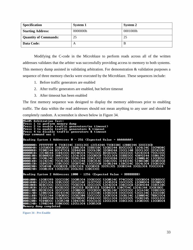
Specification System 1 System 2
Starting Address: 0000000h 0001000h
Quantity of Commands: 25 25
Data Code: A B
Modifying the C-code in the Microblaze to perform reads across all of the written
addresses validates that the arbiter was successfully providing access to memory to both systems.
This memory dump assisted in validating arbitration. For demonstration & validation purposes a
sequence of three memory checks were executed by the Microblaze. These sequences include:
1. Before traffic generators are enabled
2. After traffic generators are enabled, but before timeout
3. After timeout has been enabled
The first memory sequence was designed to display the memory addresses prior to enabling
traffic. The data within the read addresses should not mean anything to any user and should be
completely random. A screenshot is shown below in Figure 34.
Figure 34 - Pre-Enable
Page 45
34
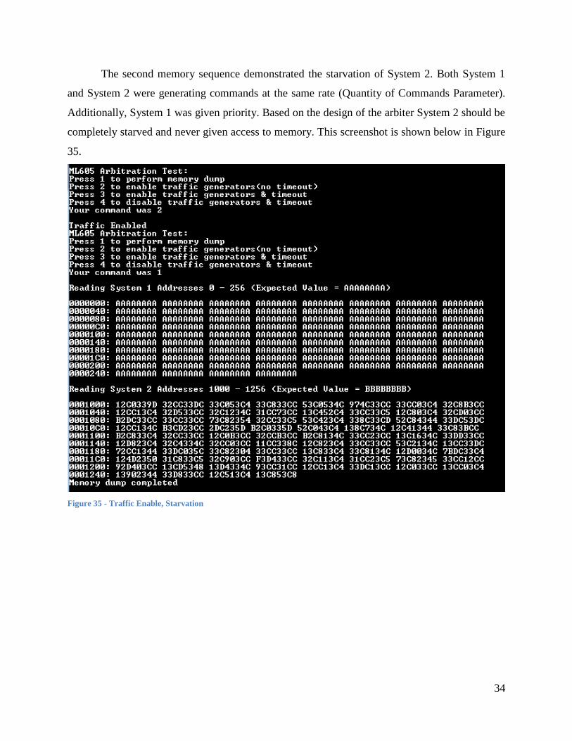
The second memory sequence demonstrated the starvation of System 2. Both System 1
and System 2 were generating commands at the same rate (Quantity of Commands Parameter).
Additionally, System 1 was given priority. Based on the design of the arbiter System 2 should be
completely starved and never given access to memory. This screenshot is shown below in Figure
35.
Figure 35 - Traffic Enable, Starvation
Page 46
35
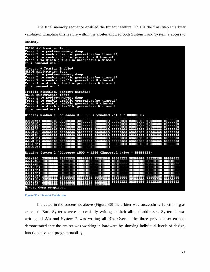
The final memory sequence enabled the timeout feature. This is the final step in arbiter
validation. Enabling this feature within the arbiter allowed both System 1 and System 2 access to
memory.
Figure 36 - Timeout Validation
Indicated in the screenshot above (Figure 36) the arbiter was successfully functioning as
expected. Both Systems were successfully writing to their allotted addresses. System 1 was
writing all A’s and System 2 was writing all B’s. Overall, the three previous screenshots
demonstrated that the arbiter was working in hardware by showing individual levels of design,
functionality, and programmability.
Page 47
36
6 Discussion
Completion of each goal in the project led to the successful design of a two system arbiter.
First, the single system interface with memory was essential in utilizing the memory and
carrying our system accesses. Second, the requirements that were set at the beginning of the
project for the arbiter were important in meeting the goals. Thirdly, the validation process was
necessary to debug and verify all key features of the design. With the success of each goal, the
arbiter can be considered validated and successful. There are still some additions and
improvements that can be made and adding these could be a useful continuation of the project.
The memory controller significantly dampened the throughput of the arbiter, as the
average access time to memory was quite high. The arbiter has a theoretical max throughput of
512 bits per cycle and is only limited by the efficiency of the memory controller and clock speed
on board. The theoretical max would only be possible with a memory controller that allowed
accesses that take only 1 cycle to complete. For the ML605 board with a 200MHz clock the
arbiter could transfer 102.4Gbps. In reality, with the memory controller that was used (average
access time of 20ns) the transfer rate is 25.6 Gbps. With a lower average access time, that
throughput could approach the max transfer rate of the arbiter. The memory controller could
definitely be improved to take full advantage of Xilinx's IP features and decrease that access time.
One of the features that might be useful to take advantage of is the back to back write commands,
which significantly improve the throughput for write commands. The timing for this is shown
below in Figure 37 , and it reaches 512 bits per 2 cycles.
Page 48
37
Figure 37: Timing for Back to Back Write Commands [14]
With regards to the arbiter itself, it could be further expanded to three or four systems. If
that were the case, adding additional arbitration schemes would be ideal since for more than two
or three systems the fixed priority arbiter would need some design changes, whereas a round
robin arbiter would be simple to implement for high number of systems. For a three system fixed
priority arbiter it would be simple to add an extra priority level for the third system and also add
the logic to handle that. Extra timeout counters would also be necessary in order to track the
timeouts for multiple systems. For n systems, there would be n-1 timeout counters for each of the
systems that have priority lower than the highest. This would allow the timeouts for each of the
systems to be independent of other systems. This is the limiting factor in adding additional
systems to the fixed priority arbiter, as it gets increasingly more complex for each addition of a
system. This is why implementation of multiple arbitration schemes is also an important addition
to the arbiter.
Additional arbitration schemes can be added within the current arbiter, and made to be
selectable by an external I/O port. Other arbitration schemes can not only be less complex to
implement for a different number of systems, but also can be more useful. With the fixed priority
arbiter, the throughput of each system can be controlled, however, in some cases the user might
like to share the resources equally. The fixed priority arbiter can do that, by setting a timeout
length of 1 cycle, however a round robin arbiter could implement that with much fewer resources.
Page 49
38
With these additions and changes the arbiter that was designed in this project can become
even more useful than it currently is. The modular design of the arbiter block makes the design
robust in that it can be used with any memory controller or FIFOs and not necessarily the Xilinx
IP cores that we used in our validation design. If improvements are to be made, the modularity of
the design should be upheld. This project not only provides a useful flexible arbiter design as set
out to do, but also provides a basis for future work in arbiter design.
Page 50
39
7 References
[1] M. Weber, "Arbiters: Design Ideas and Coding Styles," Synopsys Users Group, Boston,
2001.
[2] J. Davies, MSP430 Microcontroller Basics, Burlington: Elsevier, 2008.
[3] B. M. a. C. d. Suberbasaux, "DRAM Technology," 1997. [Online]. Available:
http://smithsonianchips.si.edu/ice/cd/MEMORY97/SEC08.PDF.
[4] SRAM Cell, [Online]. Available:
http://upload.wikimedia.org/wikipedia/commons/thumb/3/31/SRAM_Cell_%286_Transisto
rs%29.svg/250px-SRAM_Cell_%286_Transistors%29.svg.png.
[5] L. Fischer and Y. Pyatnychko, "FPGA Design for DDR3 Memory," WPI, Worcester, 2012.
[6] tfd, [Online]. Available: http://img.tfd.com/cde/DRAM.GIF.
[7] Hewlett Packard, "Memory Technology Evolution: An Overview of System Memory
Technologies," 2010.
[8] Elpida Memory, Inc., "New Features of DDR3 SDRAM," Japan, 2009.
[9] Altera Inc., [Online]. Available: http://www.altera.com.cn/literature/hb/external-
memory/emi_uniphy_ref_timing_diagram.pdf.
[10] Xilinx, Inc., "ML605 Hardware User Guide, UG534," 2012.
[11] Xilinx, Inc., "Virtex-6 Family Overview, DS150," 2012.
[12] Evertiq, [Online]. Available:
http://evertiq.com/news_images/Image_Library/Chip/Products/xilinx/xilinx_ml605-board-
l.jpg.
[13] Xilinx Inc., "Xilinx ISE Overview," [Online]. Available:
http://www.xilinx.com/itp/xilinx10/isehelp/isehelp_start.htm.
[14] Xilinx Incorporation, "Virtex-6 FPGA Memory Interface Solutions User Guide," 19
October 2011. [Online]. Available:
http://www.xilinx.com/support/documentation/ip_documentation/mig/v3_9/ug406.pdf.
[Accessed 20 April 2013].
[15] Xilinx Inc., "MicroBlaze Micro Controller System," 2012.
Page 51
40
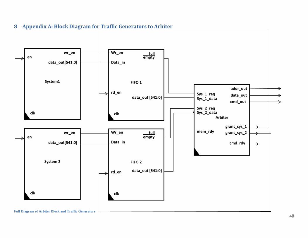
8 Appendix A: Block Diagram for Traffic Generators to Arbiter
Full Diagram of Arbiter Block and Traffic Generators
System1
wr_en
data_out[541:0] en
clk
System 2
wr_en
data_out[541:0]
en
clk
Arbiter
addr_out
data_out Sys_1_req Sys_1_data
Sys_2_req Sys_2_data
cmd_out
grant_sys_1
grant_sys_2
cmd_rdy
mem_rdy
Wr_en
rd_en
empty
FIFO 1
full
data_out [541:0]
Data_in
clk
Wr_en
rd_en
empty
FIFO 2
data_out [541:0]
Data_in
clk
full
Page 52
41
9 Appendix B: Interfacing Systems to the Arbiter Block
Appendix A showed how our traffic generators were connected to the arbiter and arbiter
block. This can serve as an example for when using external systems with our arbiter design.
There are two signals that the systems need to provide to the FIFOs. The wr_en which controls
whether or not the FIFO will write the data on the next clock edge and the data_in signal which
is the data that needs to be written.
The wr_en signal should be asserted when there is valid data on the data_in line of the
FIFO. The data_in signal is a wide signal that contains the command (3bits) (read: 001 and
write: 000), the 27 bit address to execute the command on, and in the case of a write command
the 512 data bits themselves. The order for these is {data, address, command} and this is
unpacked to individual signals when being de-queued by the arbiter.