Page 1
i
UNIVERSITY OF CALIFORNIA, SAN DIEGO
Digital-IF SiGe BiCMOS Transmitter IC for
3G WCDMA Handset Application
A dissertation submitted in partial satisfaction of the
requirements for the degree Doctor of Philosophy
in
Electrical Engineering (Electronic Circuits and Systems)
by
Vincent Wing-Ching Leung
Committee in charge:
Lawrence E. Larson, Chair Peter M. Asbeck Laurence B. Milstein Andrew C. Kummel William G. Griswold Prasad S. Gudem
2004
Page 2
ii
Copyright
Vincent Wing-Ching Leung, 2004
All rights reserved.
Page 3
iii
Signature Page
Page 4
iv
Dedication
To my wife Venus,
To our son Ivan,
& to my parents.
給明茵, 宇謙, 和我的父母親
Page 5
v
Table of Contents
SIGNATURE PAGE..........................................................................................................III
DEDICATION.................................................................................................................. IV
TABLE OF CONTENTS..................................................................................................... V
LIST OF FIGURES........................................................................................................ VIII
LIST OF TABLES ......................................................................................................... XIII
ACKNOWLEDGEMENTS ...............................................................................................XIV
VITA, PUBLICATIONS AND FIELDS OF STUDY........................................................... XVII
ABSTRACT ...................................................................................................................XIX
CHAPTER 1 INTRODUCTION ....................................................................................... 1
1.1 3G Wireless System and Wideband CDMA ...................................................... 3
1.1.1 Analog 1G and Digital 2G ....................................................................... 3
1.1.2 Vision and Evolution of 3G ..................................................................... 5
1.1.3 Wideband CDMA .................................................................................... 6
1.2 Transmitter IC for WCDMA Handset .............................................................. 10
1.2.1 Transmitter IC Fundamentals................................................................. 11
1.2.2 WCDMA Transmission Specifications.................................................. 16
1.3 SiGe BiCMOS Process..................................................................................... 22
1.3.1 SiGe HBT Basics ................................................................................... 24
1.3.2 IBM 6HP Process................................................................................... 28
1.4 Dissertation Objectives and Organization ........................................................ 31
CHAPTER 2 HIGHLY-INTEGRATED TXIC ARCHITECTURE..................................... 35
2.1 Survey of TxIC Architectures for WCDMA Handsets .................................... 36
2.1.1 Heterodyne Transmitter Architecture .................................................... 36
2.1.2 Homodyne Transmitter Architecture ..................................................... 42
2.2 Digital-IF Transmitter Architecture ................................................................. 46
Page 6
vi
2.2.1 Architecture Overview........................................................................... 46
2.2.2 Digital Quadrature Modulator................................................................ 47
2.2.3 Problem of Reconstruction (IF) Filtering............................................... 48
2.2.4 Frequency Planning Scheme.................................................................. 51
2.2.5 High-Order-Hold DAC .......................................................................... 53
2.2.6 Pulse-Shaping and Interpolation Filters................................................. 58
2.2.7 Summary of the Transmitter Architecture ............................................. 65
2.3 Spurious Emission Simulations........................................................................ 66
2.4 Summary........................................................................................................... 73
CHAPTER 3 LOW-POWER TXIC CIRCUITS.............................................................. 75
3.1 8-bit 250 Msps SOH DAC ............................................................................... 77
3.1.1 Circuit Design ........................................................................................ 77
3.1.2 Measured Results ................................................................................... 84
3.2 SSB Mixer ........................................................................................................ 93
3.2.1 Circuit Design ........................................................................................ 93
3.2.2 Measured Results ................................................................................... 99
3.3 RFVGA........................................................................................................... 105
3.3.1 Circuit Design ...................................................................................... 105
3.3.2 Measured Results ................................................................................. 108
3.4 Summary......................................................................................................... 113
CHAPTER 4 AMPLIFIER LINEARITY IMPROVEMENT BY ENVELOPE INJECTION .. 115
4.1 Linearity Analysis of Envelope Injection Technique..................................... 116
4.2 Discussions on Theoretical Results ................................................................ 121
4.3 Comparison of Measurement and Simulation Results ................................... 124
4.4 Summary......................................................................................................... 126
CHAPTER 5 MEASURED TXIC RESULTS................................................................ 127
5.1 Experimental Setup ........................................................................................ 128
5.2 Measured Results............................................................................................ 130
5.3 Summary......................................................................................................... 140
Page 7
vii
CHAPTER 6 CONCLUSIONS ..................................................................................... 142
6.1 Key Research Results ..................................................................................... 142
6.2 Directions for Future Research....................................................................... 144
REFERENCES .............................................................................................................. 146
Page 8
viii
List of Figures
Figure 1.1 Increase of mobile service subscribers over the years. .................................2
Figure 1.2 Comparison of (a) FDMA and (b) TDMA concepts.....................................5
Figure 1.3 The conceptual CDMA concept....................................................................8
Figure 1.4 Principle of spreading and despreading in CDMA. .....................................9
Figure 1.5 Block diagram of a cellular handset, showing the position of the TxIC.....11
Figure 1.6 Conceptual diagram of the quadrature modulator.......................................12
Figure 1.7 Conceptual diagram of an up-conversion single-sideband mixer. ..............15
Figure 1.8 A sample plot of measured spectral regrowth.............................................18
Figure 1.9 Spectral emission mask specifications. .......................................................19
Figure 1.10 Illustration of error vector and the related parameters. .............................20
Figure 1.11 (a) Schematic device cross section of a SiGe HBT, and (b) the micro-photographic view [48]. ..................................................................................25
Figure 1.12 Energy band diagram of a graded-base SiGe HBT compared to a Si BJT..........................................................................................................................25
Figure 1.13 SiGe HBT, whose fT is inherently higher than that of silicon for the same bias current, can trade off the excess speed to achieve a low-power solution..........................................................................................................................27
Figure 1.14 Current consumption of PA and TxIC versus the transmitter output power, and the output power probability distribution function. A poorly designed TxIC can substantially reduce overall transmitter efficiency. ........................32
Figure 2.1 Block diagram of a conventional heterodyne transmitter. ..........................38
Figure 2.2 Two variable-IF heterodyne architectures which eliminate the external IF filter by (a) implementing a complex-IF filter, and (b) adopting a frequency planning scheme..............................................................................................41
Figure 2.3 Block diagram of a typical homodyne transmitter......................................43
Figure 2.4 Heterodyne transmitter with digital IF modulator. .....................................46
Page 9
ix
Figure 2.5 Locations of digital images when (a) L = 16, and (b) L = 32. The “black” signal is the desired signal and the “white” are the digital images. ................50
Figure 2.6 Frequency planning illustration: locations of images when the channel is at (a) the lower or (b) the upper edge of the WCDMA Tx band. .......................52
Figure 2.7 Transient waveforms of (a) S/H DAC and (b) FOH DAC, and (c) their corresponding spectrum rolloffs. ....................................................................54
Figure 2.8 Signal processing of (a) a FOH DAC and (b) a Kth-order hold DAC.........56
Figure 2.9 Output waveforms of the (a) ZOH, (b) FOH, and (c) SOH DAC...............58
Figure 2.10 (a) Magnitude responses of the comb filter of order 3 to 6, and (b) the filtered 3x-upsampled spectrum. (fclk = 23.04 MHz). .....................................61
Figure 2.11 Spectrum of the 11x up-sampled signal after the 3rd-order comb filter (fclk = 253.44 MHz)................................................................................................ 62
Figure 2.12 An efficient implementation of a Nth-order comb lowpass filter for an L-times interpolation...........................................................................................62
Figure 2.13 (a) Spectrum of the digital-IF signal, and (b) the corresponding spectrum expressed in dBc over the respective measurement bandwidth......................63
Figure 2.14 Spectrum of the digital-IF signal in dBc over measurement bandwidth with 5-bit or 8-bit of resolution.......................................................................65
Figure 2.15 The proposed transmitter architecture featuring a SOH DAC. .................66
Figure 2.16 Output spectrum of the TxIC from dc to 12.5 GHz. .................................68
Figure 2.17 Simulated output spectrum of the TxIC in the DCS and WCDMA bands..........................................................................................................................69
Figure 2.18 Simulated output spectrum of the TxIC when the SOH DAC is replaced by a conventional ZOH DAC..........................................................................70
Figure 2.19 Combined magnitude responses of the RF bandpass SAW filter and the duplexer filter..................................................................................................72
Figure 2.20 Transmit signal spectrum at the antenna, expressed in dBc/ 5MHz, (a) from DC to 12.5 GHz, and (b) near the DCS/ WCDMA bands. Maximum (worst-case) TxIC output power of +24 dBm is assumed. .............................73
Figure 3.1 Block diagram of the WCDMA handset TxIC (analog/RF frontend chip). 77
Page 10
x
Figure 3.2 Simplified schematic of the SOH DAC core, featuring the dominantly capacitive load.................................................................................................78
Figure 3.3 Single-ended conceptual diagram of the 16 to 1 capacitor divider network..........................................................................................................................80
Figure 3.4 (a) Schematic of the bottom current source array (showing the MSB segment only), and (b) the plan for the complete common-centroid current source layout. ..................................................................................................83
Figure 3.5 Schematic of the IFVGA. It implements the second integrator for the SOH D/A conversion. ..............................................................................................84
Figure 3.6 Micro-photograph of the SOH DAC test cell. ............................................85
Figure 3.7 Illustration of test setup for the DAC evaluation. .......................................86
Figure 3.8 A typical probe station setup for subsystem test chip evaluation. .............. 87
Figure 3.9 (a) Measured SOH DAC output transient waveform, and (b) the measured spectrum from dc to 1 GHz. The spectrum exhibits the elevated [sin(x)/x]3 image rolloff, confirming the SOH D/A conversion behavior........................89
Figure 3.10 Measured SFDR of the SOH DAC. ..........................................................90
Figure 3.11 Measured SOH DAC two-tone (a) transient waveform and (b) spectrum..........................................................................................................................91
Figure 3.12 Measured ACLR results of the SOH DAC. .............................................. 91
Figure 3.13 Comparison of the SOH DAC to other commercial 8-bit DAC solutions regarding conversion speeds and current consumptions.................................92
Figure 3.14 Broadband 90o phase shifter. ....................................................................93
Figure 3.15 (a) Calculated phase output responses of the 90o phase shifter circuits, and (b) their differences.........................................................................................96
Figure 3.16 (a) Divide-by-two circuit for the quadrature LO generation, and (b) implementation of each latch. .........................................................................97
Figure 3.17 Implementation of mixer variable-gain through (a) a bleeder circuit, and (b) a translinear stage. The translinear circuit is more power efficient as current consumption will drop with the mixer gain simultaneously...............98
Figure 3.18 Single-sideband up-conversion mixer core............................................... 99
Page 11
xi
Figure 3.19 Micro-photograph of the single-sideband mixer test cell. ......................100
Figure 3.20 Setup for the SSB mixer experimentation...............................................100
Figure 3.21 (a) Measured mixer gain versus the control current (Ictrl), and (b) the measured total mixer current consumption versus the gain..........................101
Figure 3.22 A sample measured output spectrum of the SSB mixer. A single-tone IF input is applied for LO leakage and sideband rejection measurements........102
Figure 3.23 Measured LO and sideband rejection versus the mixer gain. .................103
Figure 3.24 Measured mixer compression behavior. .................................................103
Figure 3.25 Measured WCDMA spectrum of the SSB mixer at the maximum average output power. ................................................................................................104
Figure 3.26 Measured mixer ACLR results versus output power levels....................105
Figure 3.27 Simplified schematic of the RFVGA. The two stage design features adaptive bias schemes to make linearity requirements while minimizing the quiescent current consumptions. ................................................................... 106
Figure 3.28 Power detector bias control circuit..........................................................107
Figure 3.29 Microphotograph of the RFVGA test chip. ............................................109
Figure 3.30 Experimental setup for the RFVGA test chip evaluation. ...................... 109
Figure 3.31 Measured current consumption of the RFVGA versus the input power level...............................................................................................................110
Figure 3.32 Measured gain compression of the RFVGA versus output power level. 111
Figure 3.33 Measured ACLR of RFVGA showing the linearity improvements due to the power detector bias control. .................................................................... 112
Figure 3.34 Measured RFVGA ACLR results versus output power. Linearity improvement is observed over a wide range of power level.........................113
Figure 4.1 Conceptual diagram of the adaptive-bias RF amplifier. The power detector adjusts the dc bias in response to the input power. .......................................117
Figure 4.2 Nonlinear amplifier model, for Volterra analysis using method of nonlinear currents [89]. The fundamental signals are found by setting the nonlinear current sources to zero, while higher-order distortion voltages are evaluated by setting the signal source to zero. ..............................................................118
Page 12
xii
Figure 4.3 Vector diagram illustrating the cause of IMD3 asymmetry. Vectors 4 and represent the injected envelope signal. Note that the two resulting IMD vectors will have different amplitudes depending on the phase of the envelope. .............................................................................................122
Figure 4.4 Vector diagram showing optimal IMD3 cancellation. Note that the injected envelope signal cancels the third-order components when its phase and amplitude are optimized................................................................................124
Figure 4.5 IMD3 reduction versus input when the envelope detector is enabled. Good agreement is observed between the calculation and measured results, thus confirming the Volterra series analysis.........................................................125
Figure 4.6 Comparison between calculation and simulation of IMD asymmetry with varying envelope injection phase. Maximum IMR3 cancellation is achieved when the envelope signal is injected with the optimal phase relative to the RF inputs.............................................................................................................126
Figure 5.1 TxIC chip microphotograph. It measures 1.8 x 2.2 mm2. .........................128
Figure 5.2 Pictures of (a) the quad flat no-lead package, and (b) the bonded TxIC chip........................................................................................................................129
Figure 5.3 Experimental setup for the TxIC chip evaluation. ....................................129
Figure 5.4 (a) Laboratory bench for TxIC evaluation, and (b) close-up of the PCB. 130
Figure 5.5 (a) The measured TxIC output spectrum in the DCS and WCDMA bands. (b) Normalized and including the external filter attenuation, it is shown to meet the spurious emission requirements. ....................................................131
Figure 5.6 Measured TxIC residual sideband and LO leakage. .................................133
Figure 5.7 Measured TxIC WCDMA output spectrum (Pout = +5.5 dBm). ...............134
Figure 5.8 Measured TxIC ACLR’s versus gain control. ..........................................134
Figure 5.9 Measured occupied bandwidth of the TxIC WCDMA output. .................135
Figure 5.10 Measured TxIC noise in the WCDMA Rx band.....................................136
Figure 5.11 Measured TxIC QPSK constellation for Pout = +5.5 dBm. .....................136
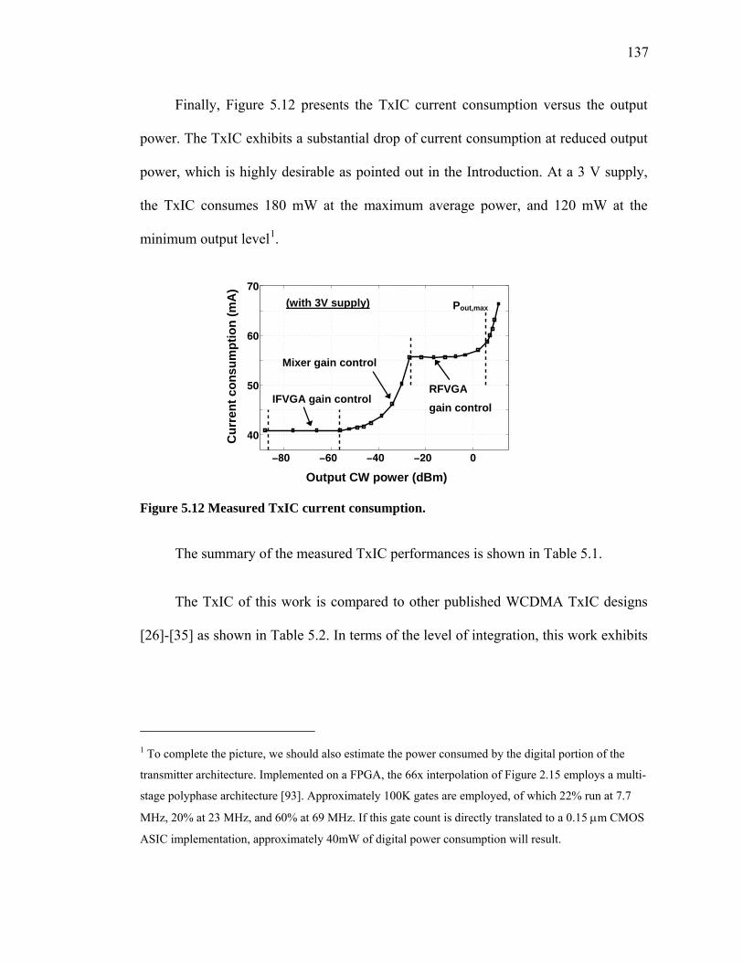
Figure 5.12 Measured TxIC current consumption. ....................................................137
Page 13
xiii
List of Tables
Table 1.1 Comparison of wireless standards: GSM, GPRS, EDGE and WCDMA.....10
Table 1.2 Spurious emission requirements for WCDMA handsets. ............................ 21
Table 1.3 Summary of WCDMA handset transmission specifications, and measured TxIC performances of published work [26]-[35]. ............................................22
Table 1.4 Summary of IBM’s 6HP SiGe BiCMOS process parameters. .....................30
Table 1.5 List of process technologies employed by the published TxIC works [26]-[35]. .................................................................................................................. 31
Table 2.1 Comparison of WCDMA TxIC Architecture. ..............................................37
Table 2.2 Comparison between the conventional S/H (ZOH) DAC and the FOH DAC...........................................................................................................................55
Table 2.3 Spurious emission specifications recalculated in dBc/5MHz. .....................71
Table 5.1 Summary of Measured TxIC performances. ..............................................139
Table 5.2 Comparison of published WCDMA TxIC work. .......................................140
Page 14
xiv
Acknowledgements
The text of Chapter Two, Three, Four and Five, in part or in full, is a reprint of the
material as it appears in Proceedings of IEEE 57th Vehicular Technology Conference,
and 2004 IEEE International Solid-State Circuits Conference (ISSCC) Digest of
Technical Papers, or has been accepted for publication in IEEE Transactions on
Vehicular Technology, and IEEE Journal of Solid-State Circuits, or has been accepted
for presentation in 2004 IEEE Custom Integrated Circuits Conference (CICC). The
dissertation author was the primary researcher and the first author listed in these
publications. He directed and supervised the research which forms the basis for these
chapters.
The past 3 years, during which this research was intensely conducted, can be
characterized as thrilling. The Ph.D. pursuit was as much a test to one’s intellectual
power as a trial to his perseverance. The journey, I must admit, was tough, which
made me particularly thankful for the support and help of many individuals.
I am uniquely advantaged to have two awesome supervisors, and I do not think I
can possibly thank them enough. Prof. Lawrence Larson had created the ideal
environment in which I could fully enjoy conducting original research. I had the best
educational experiences while learning from his profound knowledge and expertise.
And his unequivocal trust and unfailing encouragement were what got me through the
most difficult and doubtful moments. Dr. Prasad Gudem (formerly affiliated with
IBM, now with Qualcomm) is a fantastic mentor. He had substantially enriched and
Page 15
xv
refined this research with his extraordinarily sharp and intuitive perception on
technical issues. He had a genuine desire to teach and help, and had made himself
incredibly available to ensure I am well supported in all circumstances.
I am indebted to Prof. Peter Asbeck, Prof. William Griswold, Prof. Andrew
Kummel and Prof. Laurence Milstein, for their generous efforts to serve on my thesis
examination committee.
I would like to thank Semiconductor Research Corporation (SRC) and the
sponsoring companies of the “SRC SiGe Design Challenge” for the IC chip
fabrication. I also want to gratefully acknowledge the financial support from the
UCSD Center for Wireless Communications and its Member Companies, and a UC
Discovery Grant.
I thank Dr. Paul Chominski of Jaalaa and Mr. David Rowe of Sierra Monolithics
for many helpful comments and discussions. At UCSD, I would like to acknowledge
Mr. Peter Sagazio for designing and implementing the digital-IF section on a FPGA;
Ms. Karina Garcia for programming the digital pattern generator; Mr. Junxiong Deng
for assisting in Volterra series linearity analysis; and Mr. Chi-Shuen Leung for writing
an automatic test routine for a spectrum analyzer. I also want to thank other
accomplished colleagues in Prof. Larson’s and Prof. Asbeck’s groups for countless
uplifting conversations and kind laboratory assistances.
The brothers and sisters of the Chinese Bible Church of San Diego deserved my
special thanks. They were my companions in Christ, and they shared my struggles and
Page 16
xvi
joy. It is a warm feeling to know that my family is safely blanketed in their love and
care.
I express my most sincere appreciation to my wife Venus, who has
wholeheartedly put my best interest to the very top of her priorities. While I focused
on the research and could not distinguish days from nights, she had silently prayed for
me, offered support, and managed everything. She deserves all of my achievements
and honors, if any. My cheerful son Ivan was born at about the same time the silicon
chip of this research got fabricated. He had been a fountain of bliss and wonder to my
family. He had made our last year of stay in San Diego remarkably memorable, as if
“City Paradise” and gorgeous sunset were not enough.
Lastly, I would like to express my utmost gratitude to my Heavenly Father.
Without His providence and guidance, none of the amazing things mentioned above
would have happened. To me, what made the suspense of Ph.D. studies bearable was
His gracious assurance: The Lord is my shepherd, I shall not want (Psalm 23:1). My
family had truly witnessed His blessings in abundance.
Page 17
xvii
Vita
1995 B. Eng. EE (Honors), McGill University, Montreal, Canada
1997 M. Eng. EE, McGill University, Montreal, Canada Dissertation: Analysis and Compensation of Log-Domain Filter Deviations due to Transistor Nonidealities
1997-2000 Analog IC Designer, Analog Devices, Somerset, NJ
2004 Ph. D. EE, University of California, San Diego Dissertation: Digital-IF SiGe BiCMOS Transmitter IC for 3G WCDMA Handset Application
2004 Research Staff Member, IBM T.J. Watson Research Center, Yorktown Heights, NY
Publications
B. Song, V. Leung, T. Cho, D. Kang and S. Dow, “A 2.4GHz bluetooth transceiver in 0.18μm CMOS,” Proc. IEEE Asia-Pacific Conf. on ASIC, pp. 117-120, Aug. 2002.
V. Leung, L. Larson and P. Gudem, “An improved digital-IF transmitter architecture for highly-integrated WCDMA mobile terminals,” Proc. IEEE 57th Vehicular Tech. Conf., vol. 2, pp. 1335 -1339, Jeju, Korea, Apr. 2003.
V. Leung, L. Larson and P. Gudem, “An ultra-low-power SiGe BiCMOS transmitter IC for 3G WCDMA mobile phone applications,” Proc. Semiconductor Research Corporation TECHCON, Dallas TX, Aug. 2003. (The work was awarded Second Prize of the SRC SiGe Design Challenge.)
V. Leung, P. Gudem and L. Larson, “Dynamically-biased driver amplifier for WCDMA mobile phone transmitter applications,” IEEE Topical Workshop on Power Amplifiers for Wireless Communications, San Diego, CA, Sept. 2003.
V. Leung, L. Larson and P. Gudem, “Digital-IF WCDMA handset transmitter IC in 0.25um SiGe BiCMOS,” ISSCC Dig. Tech. Papers, pp. 182-183, Feb. 2004.
Page 18
xviii
V. Leung, L. Larson and P. Gudem, “An improved digital-IF transmitter architecture for highly-integrated WCDMA mobile terminals,” accepted for publication in IEEE Trans. on Vehicular Technology.
V. Leung, J. Deng, P. Gudem and L. Larson, “Analysis of envelope signal injection for improvement of RF amplifier intermodulation distortion,” to be presented at IEEE Custom Integrated Circuit Conf., Orlando, FL, Oct. 2004.
V. Leung, L. Larson and P. Gudem, “Digital-IF WCDMA handset transmitter IC in 0.25um SiGe BiCMOS,” accepted for publication in IEEE J. Solid-State Circuits (special Dec. issue on ISSCC 2004).
Fields of Study
Major Field: Electrical Engineering
Studies in Circuit and System Design for Wireless Communications. Professor Lawrence E. Larson and Dr. Prasad S. Gudem
Studies in Analog Integrated Circuit Design. Professor Gordon W. Roberts, McGill University, Montreal, Canada
Page 19
xix
Abstract
ABSTRACT OF THE DISSERTATION
Digital-IF SiGe BiCMOS Transmitter IC for 3G WCDMA Handset Application
by
Vincent Wing-Ching Leung
Doctor of Philosophy in Electrical Engineering (Electronic Circuits and Systems)
University of California, San Diego, 2004
Professor Lawrence E. Larson, Chair
The expansion of mobile communication market has been remarkable. From
originally providing voice service, the wireless industry has gradually evolved to
enable high bit-rate multi-media communications. Within the next generation (3G)
framework, the WCDMA system has emerged as a standard.
Page 20
xx
There is enormous pressure to reduce the size, cost and power consumption of
the cellular handsets. While digital circuits have experienced tremendous power
saving and enhanced functionalities with the progress of deep sub-micron processes,
the analog/RF sections remain the bottleneck. This dissertation focuses on the design
of a highly-integrated low-power transmitter IC (TxIC) in a 0.25 μm SiGe BiCMOS
technology for the WCDMA handset applications.
The TxIC employs an improved highly-integrated digital-IF architecture.
Excellent EVM performance is achieved due to the inherently mismatch-free digital
quadrature modulation. The architecture eliminates the external IF SAW filter by
adopting an optimal frequency plan and a special-purpose D/A conversion scheme
which produces high-order sin(x)/x rolloff. Spurious emission requirements are then
met with no dedicated reconstruction filter circuits. As the D/A boundary is shifted
closer to the antenna, the architecture will take full advantage of future CMOS
technology scaling.
Smart-power circuit techniques are researched. A high-speed DAC is designed
to drive a dominantly capacitive load employing very low bias current. The up-
conversion mixer, by means of a translinear transconductor, will effectively scale
down the power usage for gain control. The RF amplifier features an adaptive bias
scheme based on a power detector circuit, so that high linearity can be simultaneously
achieved with high efficiency.
Page 21
xxi
To provide further linearity improvement without increasing the quiescent
current consumption, a linearization technique based on envelope signal injection is
proposed. It is analyzed rigorously using the Volterra method, and the theoretical
predications match very well with the measured and simulated results.
Experimentations on the fabricated TxIC chip have confirmed its correct
functionality in all aspects, with state-of-the-art performance that meets WCDMA
transmission requirements. It also compares very favorably to other published work in
terms of level of integration and power consumption.
Page 22
1
CHAPTER 1 Introduction
It is hard to overstate how profoundly the advancement of cellular technology has
changed the means by which we communicate. By allowing its users to stay in touch
without being physically tied to a fixed location, and with ever improving quality and
affordability, the wireless service has become a daily necessity for a growing portion
of the population. This “anytime anywhere” voice communication allows a level of
flexibility and convenience that, once experienced, is almost inconceivable to
relinquish. The cellular technology promises to continue its penetration to our society
the way wired telephony did a century ago.
The popularity of wireless service can be best illustrated through the explosive
growth of the number of subscribers. As shown in Figure 1.1, the number of mobile
subscribers has grown over 100-fold in the past ten years [1]. Today there are over one
billion users in the world, and the number is still growing in a healthy pace. It is
expected that the global number of mobile subscribers will surpass that of the fixed
network subscribers at some point in the near future [2].
Page 23
2
Figure 1.1 Increase of mobile service subscribers over the years.
For many business and home users, wireless has already become the method of
choice for voice communication. There is also a growing demand to communicate
data in a similarly flexible (wireless) fashion, and at speeds comparable to that offered
by the wired broadband modems in office or at home. Reasonable internet access
requires several hundred kbps (kilo-bit per second) peak rate for download, while
video and picture transfer services require bit rates between a few tens of kbps to
about 2 Mbps (mega-bits per second) [3]. The third-generation (3G) technology is the
wireless industry’s answer to this high-bandwidth communication challenge.
Wideband CDMA is one standard within the 3G framework.
The advancement in wireless services has posed stiff challenges to RF IC
designers to derive cost effective, small form factor and power efficient frontend
Year 1993 1992 1994 1995 1996 1997 1998 1999 2000 2001 2002
Cel
lula
r sub
scrib
ers
(mill
ions
)
0
200
400
600
800
1000
1200
Page 24
3
solutions. This dissertation focuses on the optimal design of a 3G WCDMA SiGe
BiCMOS handset transmitter IC (TxIC).
This introductory chapter will provide the background for the research. To begin
with, we will explore the wireless evolution and put the latest 3G WCDMA standard
into perspective. It will be followed by a review on the handset transmitter functions
and the corresponding 3G specifications. Subsequently, the basics of SiGe BiCMOS,
which is the process technology for this transmitter IC development, will be provided.
We will conclude this chapter by presenting the objectives and the organization of the
dissertation.
1.1 3G Wireless System and Wideband CDMA
1.1.1 Analog 1G and Digital 2G
Cellular Telephony arrived in North America in 1983 with the rollout of the Advanced
Mobile Phone System (AMPS) [2]. Referred to as a first generation (1G) system, it
employed analog methods, in which voice signals are superimposed onto the radio
frequency (RF) carrier using frequency modulation (FM). To share the limited
spectrum among multiple mobile phone users, frequency division multiple access
(FDMA) was employed. This channel allocation scheme is straightforward as shown
in Figure 1.2(a). A user is assigned one of the (for instance, 30 kHz) channels
exclusively within the available spectrum to make the call.
Page 25
4
By offering the new-found freedom of mobile communication, the deployment
of the 1G system enjoyed great success. Demand for the service was very high,
exposing the system’s weakness of inadequate capacity. Other drawbacks of this
analog-based scheme included relatively poor call quality, limited coverage and low
security (problem of eavesdropping) [2].
To mitigate that, second generation (2G) systems employing digital technology
were deployed in the late 1980s. Message signals are digitally encoded before being
superimposed onto the RF carrier. As a result, powerful digital coding techniques can
be utilized to improve voice quality and boost immunity to channel noise and
interferences. Moreover, time division multiple access (TDMA) is applied such that
each channel was divided into time slots. Multiple simultaneous conversations can
take place at the same RF channel on a time-sharing basis, as shown in Figure 1.2(b).
The channel capacity of the 2G system was thus significantly higher than its ancestor
(where each channel is dedicated to a single conversation). Examples of 2G system
include North American Digital Cellular (NADC) [4] introduced in the U.S. in the late
1980s, and the Global System for Mobile Communication (GSM) in Europe [5] in the
early 1990s.
Page 26
5
Figure 1.2 Comparison of (a) FDMA and (b) TDMA concepts.
1.1.2 Vision and Evolution of 3G
In the 1990s, ITU (International Telecommunications Union) worked on the vision of
defining a future third generation (3G) wireless framework known as IMT-2000
(International Mobile Telecommunications-2000). Its objectives are global coverage
and a significantly enhanced data rate (over the 2G systems to support broadband
services such as internet access or multimedia communication). The target data rate
for stationary users is 2.048 Mbps. For the pedestrian and the vehicular user, the data
rates should reach 384 kbps and 144 kbps, respectively [6].
The evolution from 2G to 3G begins with the creation of robust, packet-based
data services from a pure circuit-switched-voice system [7][8]. Packet switched
communication is provided to ensure efficient resource usage for data transmission
that are bursty in nature. For example, based on the (2G) GSM standard which has a
slow data rate of 9.6-14.4 kbps, the packet mode extension is called General Packet
Radio Service (GPRS) [9]. Higher data rate is provided since GPRS can allocate
multiple time slots in parallel to a user. The assigned number of time slots is adaptive
time
frequency
Pow
er
time
frequency
Pow
er
(a) (b)
Page 27
6
to the network usage: it can be reduced in case of scarcity of resources for voice
service. GPRS service can also flexibly handle asymmetric services by allocating
different numbers of time slots in the up-link (that is, from the mobile phone user to
the basestation) and down-link (from basestation to user). The maximum data rate is
171.2 kbps in theory, and 20/30 kbps in practice. Since 3G services start at 144 kbps
(vehicular user) as described earlier, some service providers called their GPRS
implementations 2.5G to differentiate it from their 2G offerings.
As the second transitional step to 3G, Enhanced Data rates for GSM Evolution
(EDGE) [10] increases the gross bit rate by applying enhanced modulation schemes
with improved spectral efficiency. The modulation format is the 8-phase shift keying
which transmits 3 bits per symbol (instead of the Gaussian minimum shift keying
(GMSK) employed for GSM that transmits 1 bit per symbol). Data rate up to 384 kbps
can be achieved, which reaches the pedestrian user rate of the 3G target.
1.1.3 Wideband CDMA
Wideband CDMA (WCDMA) is the ultimate 3G destination of the GSM evolution. It
is selected by the European Telecommunications Standards Institute1 (ETSI) for
1 Although widely adopted in Japan and Europe, WCDMA represents only one version of the 3G
wireless standards. While the main purpose of IMT-2000 was to standardize worldwide allocation and
use of radio spectrum (a process known as “harmonization” to facilitate global roaming), there exist
five major (competing) systems within the framework [12][13] at the end due to intense political and
vendor lobbying [14]. In particular, WCDMA should not be confused with the cdma2000 standard [16]
in the U.S. Although both are based on the CDMA technology, cdma2000 has different modulation and
Page 28
7
wideband radio access to support 3G multimedia service [11]. The data networking for
WCDMA is based on GPRS/ EDGE. As a result, WCDMA service can be integrated
with the existing GSM core network cost-effectively. It adds the ability to handle 2
Mbps data rate by making use of wide-bandwidth channels of 5 MHz. The transmit
band occupies 1920-1980 MHz, while 2110-2170 MHz is reserved for receive band in
frequency division duplex (FDD) operation.
WCDMA employs code-division multiple access, or CDMA, (in oppose to the
FDMA or TDMA described before) to distinguish between users who share the
common transmission medium [16]. At the transmitter side, each user’s message
signal is encoded by a unique (orthogonal) code sequence, which is composed of
pseudo-random bits (known as “chips”) running at a much higher rate than the
information being sent. Since the bandwidth of the code signal is much larger than that
of the message, the encoding process “spreads” the signal spectrum. The encoded
message signal will share the same frequency (channel) with other users at the same
time, as shown in Figure 1.3. This is to contrast with the other two multiple access
schemes shown in Figure 1.2.
spreading schemes [17], and it adopts a different evolutionary path from its 2G IS-95 (also known as
cdmaOne) ancestor [11][15].
Page 29
8
Figure 1.3 The CDMA concept.
At the receiver side, the received signal will be correlated with a synchronously-
generated replica of the spreading code. (This implies that the receiver has knowledge
of the modulating code the transmitter applies.) Assuming the cross-correlations
between the code of the desired user and the code of other users are small (or the
spreading codes are orthogonal), the receiver will “despread” the signal of the desired
user, while the signals from other users will stay spread and appear as background
noise. As a result, within the information bandwidth, the power of the desired user will
be much larger than that of the other users, as shown in Figure 1.4. The desired signal
can be readily extracted. Notice that for similar reasons, the spread-spectrum
modulation is also robust against interferences or jamming signals.
time
frequency Po
wer
Page 30
9
Figure 1.4 Principle of spreading and despreading in CDMA.
CDMA is more susceptible to the “near-far” problem than its FDMA or TDMA
counterparts [18][19]. A weak received signal from a far-away user can be totally
overwhelmed by a strong signal from a nearby user. Since the strong signal will raise
the noise floor upon despreading, detection of the desired weak signal is greatly
degraded. To mitigate that, CDMA transmitters must feature relatively wide and
accurate power control (or specifically, signal attenuation capability) to ensure that the
signal levels presented to the basestation receiver are roughly equal (for instance,
within 1 dB of each other).
In summary, Table 1.1 compares the key air interface specifications for
WCDMA to its 2G and 2.5G ancestors. As will become evident in subsequent
chapters, the wide-bandwidth variable-envelope WCDMA signal, as well as the wide
ω
1W ( t ) t
user 1
t
user 2
ω
2W ( t )
ω
users 1 & 2
jammer
1W ( t )
ω
user 1 user 2 + jammer
transmitters receiver Air interface
t
Page 31
10
gain control range mandated for the system, will have major impacts on the RF
frontend architecture and circuit design.
Table 1.1 Comparison of wireless standards: GSM, GPRS, EDGE and WCDMA.
1.2 Transmitter IC for WCDMA Handset
As traditional low-data-rate voice-centric handsets evolve to advanced high-data-rate
feature-rich “smart” phones, the mobile radio design sees a substantial increase in
complexity [1]. But as the 3G wireless system gains popularity, there is also an
enormous pressure to reduce the size, cost and power consumption of the mobile
phone chipset [20][21]. While the digital baseband part has experienced tremendous
power saving and functionality enhancement due to the progress of deep submicron
GSM GPRS EDGE WCDMA
Generation 2G 2.5G 2.5G 3G
Uplink Freq. (MHz) EGSM: 925-960, DCS:1805-1910 1920-1980
Downlink Freq. (MHz) EGSM: 880-915, DCS: 1710-1785 2110-2170
Channel BW (MHz) 0.2 0.2 0.2 5
Multiple Access TDMA TDMA TDMA CDMA
Duplexing Frequency Division Duplexing
Modulation GMSK GMSK 8-PSK QPSK (with Hybrid PSK spreading)
Signal envelope Constant Constant Variable Variable
Power control range Small (about 25 dB) Wide (>74 dB)
Data Rate (kbps) 9.6 – 14.4 171.2 384 2048
Page 32
11
technologies, the analog/RF sections of the mobile radio remain the bottleneck in
achieving a low-power high-performance solution.
This dissertation focuses on the innovative design of the transmitter IC (TxIC), a
key RF component on the 3G WCDMA handset solution [22]-[35]. The TxIC
contributes significantly to the evaluation of part count (which translates to cost), size
and the battery life of the final handset solution.
1.2.1 Transmitter IC Fundamentals
The TxIC is located between the digital signal processor (DSP) and the power
amplifier (PA) as shown in Figure 1.5. Interfacing between the digital and the
analog/RF domains, it faithfully translates the baseband data into a format suitable for
transmission to the basestation. Specifically, the translation operation entails: (1)
quadrature modulation of baseband data, (2) up-conversion to the radio frequencies,
and (3) power control. (Notice that the distinctions are made only for the sake of
conceptual clarity; these functions, especially the first two, are often achieved
simultaneously.) These concepts are discussed below [18].
Figure 1.5 Block diagram of a cellular handset, showing the position of the TxIC.
transmitter PA SAW
Dup
lexe
r
receiver SAW DSP
this work
Page 33
12
WCDMA system employs QPSK (quadrature phase shift keying) as its uplink
(from handset to basestation) modulation scheme [39]. The in-phase and quadrature-
phase baseband signals2, Ix ( t ) and Qx ( t ) , are impressed upon a single carrier (of
radian frequency ωc ) according to
ω ωQPSK I c Q cx ( t ) x ( t )cos( t ) x ( t )sin( t )= + (1.1)
This operation is accomplished by the quadrature (I/Q) modulator as shown in Figure
1.6. Two mixer circuits are employed. The modulator is a direct up-converter that
transforms the (5 MHz wideband spread) spectrum of each baseband signal to the
(intermediate-frequency IF, or the RF) carrier frequency. Ideally, it suppresses the
carrier signal ( ωccos( t )), and preserves the orthogonal signal relationships.
Figure 1.6 Conceptual diagram of the quadrature modulator.
2 To tighten the bandwidth of the modulated spectrum, and to achieve Nyquist signaling for zero inter-
symbol interference (ISI) [36], the baseband data Ix ( t ) and Qx ( t ) are generated by pulse-shaping
the symbols on a HPSK constellation [37] by a root-raised-cosine filter with α = 0.22 [39].
cos(ωct)
xI(t)
xQ(t)
Σ
sin(ωct)
xQPSK(t)
Page 34
13
In practice, however, the accuracy of the I/Q modulation (or the quality of the
transmit signal) is plagued by LO leakage and I/Q leakage (imperfect carrier signal
orthogonality) [38]. These nonideal effects can be explicitly incorporated into (1.1) to
give:
Δ1 ω Δθ ωQPSK I I ,dc c Q Q,dc cnonideal
Ax ( t ) ( x ( t ) x ) cos( t ) ( x ( t ) x ) sin( t )A
⎛ ⎞= + ⋅ + ⋅ + + + ⋅⎜ ⎟⎝ ⎠
(1.2)
where I ,dcx , Q,dcx denote the dc offsets associated with the baseband data, while
ΔA A , Δθ represent the gain and phase mismatches between the I and Q channels,
respectively. The dc offset can be caused by device mismatches at the analog
baseband circuits (before the quadrature modulator) as well as within the mixer
circuits. Because of them, a portion of the carrier signal appears at (or leaks to) the
output of the mixer. On the other hand, the I/Q leakage is due to the gain and phase
imbalances between the quadrature local oscillator (LO) carrier signals (as well as the
mixer circuits). As a result, the outputs of the mixers are not orthogonal and actually
corrupt, or spill into, each other. The leakage power can be found by [19]:
2 2 1 Δ Δθ Δ2 2 1 Δ Δθ Δ
leakage
desired
P A A cos A AP A A cos A A
− + ⋅ +≈
+ + ⋅ + (1.3)
For instance, gain and phase mismatches of 2% and 2o respectively would cause an
I/Q leakage of -35 dBc.
Page 35
14
In general, an ideal up-conversion mixer produces an output whose amplitude is
proportional to the input signal only. The output should be independent of the LO
signals. In fact, for noise and gain reasons, it is very desirable to drive the mixers with
square waves (instead of sinusoids) LO’s, and operate the mixers as on-off switches
(instead of multipliers) [18]. Square waves have strong odd harmonics and somewhat
significant even harmonics if the duty cycle is not exactly 50%. Due to the spectrally-
rich LO’s and, and to a lesser extent, the harmonic and intermodulation distortions of
the mixer circuit itself, mixing products (spurs) will appear at frequencies given by
spur LO IFf m f n f= ⋅ ± ⋅ (1.4)
where LOf denotes the LO frequency, IFf the input signal (intermediate) frequency,
and m, n are integers ranging from 0 to +∞ . Assuming the up-conversion employs
low-side injection, the desired output is given by LO IFf f+ (that is, 1m n= = ). All
other combinations of ( )m,n denote undesirable spurious emissions, which should be
minimized to prevent polluting the airwaves where a multitude of transmissions (of
different wireless standards) co-exist. In practice, the amplitudes of the spurs decrease
as m or n increases.
For example, strong LO leakage would appear at LOf ( 1 0m ,n= = ). It is usually
suppressed by employing a doubly-balanced (Gilbert) mixer architecture [18].
Besides, an undesirable sideband output, which has equal amplitude as the desirable
one, appears at LO IFf f− (at equal distance from the LO frequency on the opposite
Page 36
15
side). The sideband can be eliminated by a discrete RF surface acoustic wave (SAW)
filter, which is appropriately known as the image-reject filter. For an integrated
solution, the single-sideband (SSB) mixer architecture [18] of Figure 1.7 can be
employed.
Figure 1.7 Conceptual diagram of an up-conversion single-sideband mixer.
Before we leave this section, let’s investigate a key QPSK signal property that
has crucial influence on the transmitter (and in particular, the RF amplifier) circuit
design. From (1.1), the QPSK-modulated waveform is equivalently written as
ω θQPSK cx ( t ) A( t )cos[ t ( t )]= + (1.5)
where
2 2 1θ QI Q
I
x ( t )A( t ) x ( t ) x ( t ) & ( t ) tan
x ( t )− −⎛ ⎞
= + = ⎜ ⎟⎝ ⎠
(1.6)
As shown in (1.6), the envelope signal A( t ) is signal-dependent. In other words,
QPSK is a “variable-envelope” (linear) modulation scheme. Circuit linearity is of
paramount importance to preserve the information integrity. Besides, circuit
cos(ωct)
xIF(t) Σ
sin(ωct)
XRF(t)
90o
Page 37
16
distortions will spread the frequency spectrum of the variable-envelope signal to
adjacent channels. Known as “spectral regrowth”, this phenomenon is detrimental to
system capacity. The linearity requirement is usually the most stringent for the RF
amplification stage (or the PA driver located at the end of the TxIC path), which
handles the highest signal level. This inevitably translates to relatively inefficient
amplifier designs. The design of high-linearity high-efficiency RF amplifier is further
complicated by the need of power control, or the very wide range of signal levels the
amplifier will handle. The amplifier should produce high average (not just peak)
efficiency, which takes the statistical signal power distribution into account.
Based on the understanding of the transmitter system fundamentals, we can now
move on to describe the handset transmitter specifications set forth by the WCDMA
standardization body.
1.2.2 WCDMA Transmission Specifications
The WCDMA handset transmission specifications are given in [39], which is available
on the 3rd generation Partnership Project (3GPP) website [40]. Note that the
performance requirements are defined for the entire transmitter path up to the antenna,
while the TxIC is only one of the contributing components. Therefore, the TxIC
should be designed with good safety margins so that when additional impairments are
introduced further along the path (most noticeably, by the PA), system requirements
are still met. Key performance metrics pertaining to the TxIC design are highlighted
and explained below.
Page 38
17
To combat the near-far problem, closed-loop control of the transmitter output
power must be implemented as described earlier. WCDMA User Equipment (or the
handset) Power Class 3 targets a maximum transmission power level of +24 dBm, and
a minimum of -50 dBm, at the antenna. This corresponds to a very wide power control
range of 74 dB. Since it is not cost-effective to build a variable-gain PA, the power
control range will be realized totally by the TxIC. To account for process, supply and
temperature variations, most manufacturers implement close to 90 dB of dynamic
range into their TxIC’s [26]-[32],[34]-[35]. On the other hand, typical WCDMA PA’s
feature power gain around 25 dB [30],[41]-[43]. Therefore, the TxIC should furnish a
maximum output power of about +5 dBm to meet the maximum transmission power
level (while accounting for additional insertion losses of approximately 2 to 3 dB due
to, for example, the duplexer filter).
The linearity of the transmitter is specified in terms of Adjacent Channel
Leakage Ratio (ACLR). A measure of spectral regrowth, ACLR is the ratio of the
power measured in the adjacent channel to the transmitted power as shown in Figure
1.8. The maximum allowable ACLR at 5 MHz offset (for first adjacent channel) and
10 MHz offset (for alternative adjacent channel) are -33 dBc and -43 dBc,
respectively. These levels must be maintained as long as the adjacent channel power is
greater than -50 dBm. To provide a safety margins for the PA distortions, the ACLR
of the TxIC should be at least 10 dB better than minimum requirements, and equal -43
and -53 dBc at 5 and 10 MHz offsets, respectively.
Page 39
18
Figure 1.8 A sample plot of measured spectral regrowth.
The shape of the RF transmission spectrum is further governed by the Occupied
Bandwidth and the Spectral Emission Mask requirements. The first requirement
specifies that at least 99% of the transmitted power must fit within a 5 MHz bandwidth
at the chip rate of 3.84 MHz. The second requirement defines the maximum tolerable
unwanted emissions immediately outside the nominal channel between 2.5 MHz and
12.5 MHz offset from the center carrier frequency. (The power of emission is
measured in 30 kHz bandwidth if it is between 2.5 to 3.5 MHz offset frequency, and 1
MHz in the 3.5 to 12.5 MHz region. The out of channel emission is specified relative
to the channel power measured in a 3.84 MHz bandwidth.) These emissions are caused
by the modulation process and transmitter distortion, and should not be confused with
the spurious emissions caused by up-conversion process. The spectral emission mask
requirement is graphically displayed in Figure 1.9.
Frequency in MHz
1935 1940 1945 1950 1955 1960 1965
−70
−60
−50
−40
−30
−20
−10
0
Spec
trum
in d
Bm
transmit channel Adjacent channel leakage
Alternative channel leakage
5 MHz bandwidth
Page 40
19
Figure 1.9 Spectral emission mask specifications.
The transmitted waveform quality, or the modulation accuracy, is represented by
the performance metric known as root-mean-square (rms) Error Vector Magnitude
(EVM). Error vector is defined as the displacement of the actual measured symbol
from its theoretical constellation position, as shown in Figure 1.10. RMS EVM is
given by the square root of the ratio of the mean error vector power to the mean
reference signal power expressed as a percentage. It shall not exceed 17.5 % for output
power levels greater than -20 dBm. Typically, about 5 to 10 % of EVM is budgeted
for the TxIC.
0 2 2.5 3.5 6 8 9 10 12.5−60
−50
−40
−30
−20
−10
0
10
Frequency offset from carrier (MHz)
Spec
tral
mas
k in
dB
c/B
W
Measurement bandwidth (BW): 1 MHz (over this region) 30 KHz3.84 MHz
spectral emission mask specs.
Page 41
20
Figure 1.10 Illustration of error vector and the related parameters.
As mentioned earlier, spurious emissions are caused by frequency up-conversion
products, circuit harmonic and intermodulation products, as well as circuit noise. They
must be minimized to avoid degrading the sensitivity of the WCDMA receiver, or
“jamming” nearby receivers operating at different standards. These limits are
summarized in Table 1.2, which defines general and additional spurious emission
requirements in terms of the output power (dBm) over the respective measurement
bandwidth. The design criteria given in [31] are also adopted. Since the specifications
are specified at the antenna, proper adjustments, such as those to be described in
Section 2.3, should be made when evaluating whether the TxIC is meeting the
spurious emission requirements.
I
Q
Ideal signal (reference)
Measured signal Error vector
ΔA
Δθ ΔA = I/Q magnitude mismatch error
Δθ = I/Q phase mismatch error
Page 42
21
Table 1.2 Spurious emission requirements for WCDMA handsets.
The key 3GPP WCDMA transmission requirements and the TxIC budgets are
summarized in Table 1.3. Measured performances of ten TxIC3 [26]-[35] are also
presented alongside for reference purposes. The measured data match quite closely to
the TxIC design budgets discussed earlier, which support our analysis.
3 These ten TxIC’s are among the most advanced and highly-integrated solutions reported today. (On
the other hand, for conciseness purpose, the chips that only integrate the IF section [22]-[25] are
omitted in the comparison.) They represent a rich sample of architecture and circuit design techniques,
and are implemented in different silicon processes. Further comparisons (including the TxIC of this
research) will be made in subsequent chapters when appropriate.
Frequency bandwidth
Measurement bandwidth
Minimum requirement
Frequency band
9 - 150 kHz 1 kHz -36 dBm
0.15 - 30 MHz 10 kHz -36 dBm
30 - 1000 MHz 100 kHz -36 dBm
General spurious
emissions [39]
1 - 12.75 GHz 1 MHz -30 dBm
1893.5 - 1919.6 MHz 300 kHz -41 dBm PHS
925 - 935 MHz 100 kHz -67 dBm EGSM
935 - 960 MHz 100 kHz -79 dBm GSM
Additional Spurious emissions
[39]
1805 - 1880 MHz 100 kHz -71 dBm DCS Rx
1920 - 1980 MHz 1 MHz -25 dBm WCDMA Tx
2110 - 2170 MHz 3.84 MHz -120 dBm WCDMA Rx Other [31]
1710 - 1785 MHz 100 kHz -49 dBm DCS Tx
Page 43
22
Table 1.3 Summary of WCDMA handset transmission specifications, and
measured TxIC performances of published work [26]-[35].
To meet the stringent RF performances mandated by WCDMA standard cost
effectively, the TxIC of this research will be implemented on the SiGe BiCMOS
process, as discussed in the next section.
1.3 SiGe BiCMOS Process
Performance, cost and time-to-market are the three critical factors influencing the
choice of technologies in the competitive RF industry [19]. For the handset RF
Specifications/ Institutions [ref.]
Pout (dBm)
Gain (dB)
ACLR @ 5MHz
(dB)
ACLR @ 10MHz
(dB)
Occupied BW
(MHz) EVM (%)
3GPP Specs. +24 74 -33 -43 5 17.5
TxIC Budget ~ +5 90 -43 -53 4.5 5-10
Mitsubishi [26] +7 89.9 -47.6 -68.2 4.2 6.3
IBM [27] +7 95 -49 N/A N/A 6.3
Mitsubishi [28] +7 90.5 -45.6 -62.4 4.3 N/A
TI [29] +6 > 90 -43.7 -61 N/A 6
Philips [30] +5.5 81 -44.4 N/A N/A N/A
IBM [31] +3 115 -47 -65 N/A 2.45
Swiss ETH [32] -8 78 N/A N/A N/A 3.2
Seoul Nat. U. [33] +6 50 -38 N/A N/A N/A
Swiss ETH [34] +2.5 100 -38 -64 N/A 4.3
Qualcomm [35] +10 > 90 ~ -55 N/A N/A N/A
Page 44
23
frontend design in particular, a process’s performance is judged mainly by the speed,
linearity, noise and breakdown voltage properties of the transistors, the degree of
substrate isolation (or the availability of any specialized inter-device structures to that
effect), as well as the portfolio of passive elements it offers (which include, for
instance, high-linearity metal-insulator-metal (MiM) capacitors and high-Q metal
spiral inductors). Cost is dictated by the technology’s fabrication process and yield,
and the level of integration it supports. In that regard, the compound (III-V)
technologies such as GaAs or InP serve the high-cost low-integration (but the highest
speed and power) space, while the conventional Silicon (Si) processes, especially the
digital CMOS, serve the other end. Time-to-market is closely related to the process
maturity, accuracy of its device model at the intended speed of operation, and
sophistication of the supporting design tools and library.
Silicon-Germanium (SiGe) BiCMOS technology has a unique appeal to the
wireless marketplace by offering the high performances of III-V heterojunction
bipolar transistors (HBT’s), but with the integration (and cost) benefits of
conventional silicon processes [44]. The first standard high-volume SiGe chip was
introduced by IBM Microelectronics (Fishkill, NY and Burlington, VT) in October,
1998 [45]. Since then it has been adopted by a wide range of companies for a wide
variety of applications. Our TxIC research will be conducted on IBM’s 6HP (0.25 μm)
SiGe BiCMOS process [46], which is the second lithography generation of technology
offering. The process’s performances and integration level are important enabling
Page 45
24
factors for the TxIC architecture and circuit innovations, and the process’s maturity
helps to yield the first-pass silicon success on the experimental prototype.
1.3.1 SiGe HBT Basics
While silicon-based IC’s are superbly manufacturable, silicon is hardly the ideal
semiconductor because of its low carrier mobility and saturation velocity (as compared
to the III-V compounds). However, silicon’s speed can be vastly increased if strained
silicon-germanium alloy, whose energy bandgap is smaller than that for silicon, is
applied to “bandgap-engineer” the silicon material system [47]. Using an epitaxial
growth technique such as UHV/CVD4, films of the SiGe alloy can be deposited on the
base region of a conventional bipolar junction transistor (BJT) as shown in Figure
1.11. The p-SiGe base thus creates heterojunctions at the emitter-base (EB, n+-Si/p-
SiGe) and the base-collector (BC, p-SiGe/n-Si) junctions, hence the name
Heterojunction Bipolar Transistor (HBT).
4 UHV/CVD stands for ultrahigh vacuum chemical vapor deposition [49]. Apart from this step, the
HBT device is essentially identical to conventional silicon BJT, and is built with processing equipment
common to any advanced silicon fabrication facility. For example, the 6HP process is manufactured
using standard 200 mm silicon CMOS production tooling [46]. Therefore, the SiGe BiCMOS process
can enjoy the same low-cost and high-volume characteristics of other conventional CMOS
technologies.
Page 46
25
Figure 1.11 (a) Schematic device cross section of a SiGe HBT, and (b) the micro-
photographic view [48].
The germanium content is compositionally graded from low concentration at EB
junction to high concentration at the BC junction. This results in the energy-band
diagram as shown in Figure 1.12. It consists of a finite band offset at the EB junction
[Δ 0g ,GeE ( x )= ] as well as the larger band offset at the BC junction [Δ g ,Ge bE ( x W )= ].
The position dependence of the band offset (with respect to Si) is conveniently
expressed as a bandgap grading term:
Figure 1.12 Energy band diagram of a graded-base SiGe HBT compared to a Si BJT.
(a) (b)
EB C
SiGe
Page 47
26
Δ Δ Δ 0g ,Ge g ,Ge b g ,GeE ( grade ) E (W ) E ( )= − (1.7)
This position-dependent conduction band edge induces an electric field in the device,
which rapidly accelerates injected minority carriers (electrons) as they traverse the
base. The base transit time ( τb ), as compared to an identically constructed Si BJT, is
reduced according to [50]:
Δτ 2 11
τ η Δ Δ
g ,GeE ( grade ) kTb,SiGe
b,Si g ,Ge g ,Ge
kT eE ( grade ) E ( grade ) kT
−⎛ ⎞ ⎡ ⎤−= ⋅ ⋅ −⎜ ⎟ ⎢ ⎥⎜ ⎟ ⎢ ⎥⎝ ⎠ ⎣ ⎦
(1.8)
where η nb nbD ( SiGe ) D ( Si )= accounts for the difference between the electron and
hole mobilities in the base. For RF applications, an important figure of merit for
transistor speed is the unity (current) gain cutoff frequency ( Tf ), which is given by
( )1
1 τT eb bc bm
f C Cg
−⎡ ⎤
≈ + +⎢ ⎥⎣ ⎦
(1.9)
where mg is the transconductance ( C TI V ), and ebC , bcC are the EB and BC junction
capacitances, respectively. The smaller transit time (minority carrier traverse more
speedily across the base) of HBT explains its substantial speed advantage in terms of
the increased Tf . For handset transceiver design where low power consumption is of
paramount importance, one can advantageously operate the SiGe HBT at a frequency
below the peak Tf with a significantly reduced bias current. This frequency-power
dissipation tradeoff is illustrated in Figure 1.13.
Page 48
27
Figure 1.13 SiGe HBT, whose fT is inherently higher than that of silicon for the same bias
current, can trade off the excess speed to achieve a low-power solution.
Beside its speed advantage, HBT can also furnish a substantially higher current
gain (β ). It is because the bandgap reduction at the EB junction lowers the potential
barrier, so more electrons will be injected from emitter to base (or higher collector
current will result) for a given voltage bias. For applications (such as the handset TxIC
design) where high β is not particularly important, the process can tradeoff the HBT’s
excess β for lower base resistance ( br ) by doping the base region more heavily. This
would very advantageously lower the broadband noise of the device, and increase the
unity power-gain (or maximum oscillation) frequency, maxf according to
8π
Tmax
bc b
ffC r
= (1.10)
The introduction of the graded SiGe alloy also increases the Early voltage ( AV )
of the resulting HBT. Physically, as the base profile is more heavily weighted towards
the collector region, base region becomes harder to deplete when the collector-base
Page 49
28
voltage is increased. The higher AV translates to the higher output resistance of the
HBT, which is very beneficial for analog (or in our case, the mixed-signal part of the
TxIC) design.
The other key process issue for RF applications is the breakdown voltage of the
device, which influences the dynamic range of operation. The HBT device is
fundamentally limited by avalanche multiplication in the collector-base region [51].
Nevertheless, breakdown voltage of HBT is typically higher than that of the MOSFET
at a given Tf , which is caused by hot electron degradation of threshold voltage [52].
This makes HBT device attractive for the TxIC design, where a high output power
level is delivered.
1.3.2 IBM 6HP Process
The high-performance HBT is of little use for the wireless frontend space if the
process does not integrate a menu of high-quality passive elements and fine-geometry
CMOS transistors. The ideal technology, as well as the tool set that accompanying it,
must support building monolithic analog/ RF building blocks with the ultimate goal of
integrating the entire radio on a chip [52].
The BiCMOS 6HP process [46][53] is a versatile process integrating a 47 GHz
SiGe HBT with a 2.5 V, 0.25 μm (0.18 um effective gate length) CMOS base. Two
versions of HBT’s are incorporated: a standard high-speed (pedestal) device, and a
high (break-down) voltage device with a modified collector. Two versions of
Page 50
29
complementary MOSFET devices are provided: a standard 2.5 V 0.25 μm FET (with 5
nm gate-oxide), and a high-voltage FET (3.3 V, with 7 nm gate-oxide) for use in I/O
circuits and analog designs. It offers five levels of metal for layout flexibility. In
addition, the process features a nitride dielectric for linear MiM capacitors [54] (with
high capacitance-to-area ratio), and a top thick (analog) metal for high Q spiral
inductors [55].
The substrate also plays a crucial role on the RF frontend design [52]. For our
TxIC design in particular, undesired spurious signals (such as digital switching noise,
or harmonics of LO) can capacitively couple into the conductive substrate and corrupt
the transmitter output. The 6HP process offers a deep trench structure, as well as the
conventional (p+/n-well) guard rings, for improved isolation.
A summary of 6HP process parameters is given in Table 1.4 [46]. To
demonstrate the degree of pervasiveness of the SiGe BiCMOS in the 3G WCDMA
TxIC space, we compare the technologies employed by the ten published TxIC works
in Table 1.5. Six out of the ten TxIC’s are implemented in various versions of SiGe. If
only commercial projects are considered (that is, [26]-[31],[35]), six out of seven chips
are SiGe BiCMOS. The overwhelming majority of SiGe BiCMOS implementation
clearly demonstrates the popularity of the process for handset transmitter frontend
applications.
Page 51
30
Table 1.4 Summary of IBM’s 6HP SiGe BiCMOS process parameters.
SiGe HBT NPNs HIGH-SPEED DEVICE HIGH-VOLTAGE DEVICE
Beta 100 88
fT (Vcb=1V) 47 GHz 27 GHz
fmax 65 GHz 55 GHz
Early voltage 75 V 180 V
BVceo 3.35 V 5.4 V
FETs NFET 2.5 V PFET 2.5 V NFET 3.3 V PFET 3.3 V
Tox 5.0 nm 7.0 nm 5.0 nm 7.0 nm
Leff 0.18 μm 0.26 μm 0.18 μm 0.265 μm
IDsat 595 μA/ μm 580 μA/ μm 280 μA/ μm 285 μA/ μm
Capacitors
MOS Cap 3.10 fF/μm2
MiM Cap 0.70 fF/μm2
Resistors
Polysilicon 1 & 2 3600 Ω/ & 210 Ω/
Silicon 1 & 2 100 Ω/ & 63 Ω/
Spiral Inductors 0.28 - 83 nH, with outer dimension 100 – 450 μm
Page 52
31
Table 1.5 List of process technologies employed by the published TxIC works
[26]-[35].
1.4 Dissertation Objectives and Organization
This dissertation presents an innovative SiGe BiCMOS transmitter IC for 3G
WCDMA handset applications. The two design objectives are (1) high level of
integration, (2) and low power consumption, as explained below:
Existing TxIC solutions commonly require external filters at the intermediate
frequency (IF) for spurious rejection [22]-[29]. While being a time-proven approach,
those off-chip components (for instance, IF SAW or LC tank) are bulky and
expensive. Their successful elimination would substantially reduce the feature size and
Institutions [ref.] Process Lithography (μm) Supply (V)
Mitsubishi [26] SiGe BiCMOS 0.5 3.0
IBM [27] SiGe BiCMOS 0.5 3.0
Mitsubishi [28] SiGe BiCMOS 0.25 3.0
TI [29] SiGe BiCMOS 0.3 2.7
Philips [30] BiCMOS 0.25 2.6 – 3.0
IBM [31] SiGe BiCMOS 0.25 2.85
Swiss ETH [32] CMOS 0.25 2.5
Seoul Nat. U. [33] CMOS 0.35 3.3
Swiss ETH [34] CMOS 0.13 1.5
Qualcomm [35] SiGe BiCMOS 0.4 2.7 – 3.0
Page 53
32
cost of the final cell phone product. Therefore, it is obvious that a highly-integrated
TxIC is very desirable. However, one may question the necessity of a low-power TxIC
solution, especially in the presence of a presumably far more power-hungry PA. As
explained earlier, the WCDMA system features a wide dynamic range power control
function, to combat the “near-far” problem. Although the PA can consume a high
current at the peak output level, the power consumption drops substantially during the
power backoff mode (due to its Class AB bias) [56]. This is shown in Figure 1.14.
Moreover, at the highest probability output power, as shown by the 0 dBm point of
Figure 1.14, the PA can consume less power than a typical TxIC. This makes the TxIC
the major determinant of the overall average transmit power efficiency. As a result, a
carefully-designed low-power TxIC (as shown by the broken line in Figure 1.14) is
crucial to prolong the battery life.
Figure 1.14 Current consumption of PA and TxIC versus the transmitter output power,
and the output power probability distribution function. A poorly designed TxIC can
substantially reduce overall transmitter efficiency.
typical TxIC
PA
Pout (dBm)
0
1
2
3
4
5
-30 -20 -10 0 10 20 30 0
200
400
600
desired TxIC
Prob
abili
ty (%
)
Idc
(mA
)
CDMA Development Group (1997)
Page 54
33
The highly-integrated low-power TxIC is achieved through a combination of
architecture and circuit innovations. The dissertation is organized as follows:
Chapter 2 presents the highly integrated TxIC architecture. We will begin with a
thorough review of the existing TxIC solutions to illustrate the issues faced by
WCDMA transmitter architecture design. We will then introduce the improved
transmitter architecture based on the digital IF scheme. Two key features (namely the
optimal frequency plan and the special-purpose high-order-hold D/A conversion) are
developed to enhance the level of integration and to reduce circuit complexity.
System-level simulation results will be produced to establish that the WCDMA
spurious-emission requirements are met with virtually no dedicated IF filters.
Chapter 3 describes the low-power TxIC circuits, which include the digital-to-
analog converter (DAC), the single-sideband (SSB) mixer, and the RF variable-gain
amplifier (RFVGA). The design techniques for the three subsystems will be explained
in detail. The DAC employs a capacitor divider network to simultaneously achieve
low-power consumption and high-speed conversion. The mixer and the amplifier
employ adaptive biases to minimize the quiescent power consumption and to provide
current boost only when needed. For each case, experimental results are furnished to
demonstrate the circuits’ performances and practicality.
Chapter 4 analyzes the linearity of the RF amplifier (of the previous chapter)
meticulously, using the Volterra technique. It will be shown that the amplifier’s
linearity (in terms of intermodulation distortion) can be dramatically improved by
Page 55
34
optimally injecting the envelope signal (which is generated by the adaptive bias
control circuit) back into the main bias network. The analysis is confirmed by
comparing the theoretical predictions to simulation and experimental results.
Chapter 5 provides the measured results of the complete TxIC. Key system-level
performance metrics, such as spurious emissions, LO and sideband leakage, ACLR,
and EVM will be presented and discussed. The level of integration and the power
consumption of this work will be compared to other state-of-the-art solutions.
Chapter 6 concludes the dissertation. It summarizes the architecture and circuit
innovations of the WCDMA TxIC, and discusses the implications to future-generation
transmitter design. Future areas of research will also be suggested.
Page 56
35
CHAPTER 2 Highly-Integrated TxIC Architecture
There is enormous pressure to reduce the size, cost and power consumption of mobile
phones, as these qualities are strongly correlated to customer satisfaction. While the
digital circuits have experienced tremendous power saving and enhanced
functionalities with the progress of deep sub-micron processes, the analog/ RF
sections remain the bottleneck. In this chapter, we focus on an improved WCDMA
transmitter IC architecture for handset applications.
Existing TxIC solutions commonly require external filters at the intermediate
frequency (IF) for rejection of spurious components [22]-[29]. While being a time-
proven approach, those off-chip components (for instance, IF SAW and LC tank) are
bulky and expensive. They substantially increase the feature size and cost of the final
cell phone product.
TxIC solutions available today tend to be complicated. This is mainly due to the
heterodyne architecture [22]-[29], which demands two pairs of analog/ RF mixers and
synthesizers. Furthermore, the power consumption can be substantially driven up if an
active IF filter is integrated [30].
Page 57
36
A highly-integrated, simple and low-power WCDMA TxIC solution for mobile
station applications is proposed. This is achieved through a novel architecture which
alleviates some of the analog circuit complexities by high-speed digital signal
processing. We believe this is an appealing technological direction because the
resulting TxIC solution can then take full advantage of the rapid advancement of fine-
geometry IC technologies.
To begin with, existing TxIC architecture solutions developed by both the
industry and the academia will be reviewed. This is to illustrate the issues faced by
WCDMA transmitter architecture design. Then, we will introduce the improved
transmitter architecture based on the digital IF scheme. The design innovations
developed to enhance the level of integration and to reduce circuit complexity will be
discussed in detail. System level simulations on the spurious emission will be
presented, which is followed by concluding remarks.
2.1 Survey of TxIC Architectures for WCDMA Handsets
A list of published WCDMA handset transmitter designs [26]-[35] is shown in Table
2.1. The architectures of the TxIC’s fall into two camps: the heterodyne or the
homodyne. Their relative strengths and weaknesses are discussed below.
2.1.1 Heterodyne Transmitter Architecture
The majority of commercial WCDMA TxIC’s are heterodyne [26]-[31], performing
up-conversion in 2 steps similar to that shown in Figure 2.1. Baseband data are first
Page 58
37
up-converted by quadrature modulation to the intermediate frequency, typically at
hundreds of MHz. The in-phase (I) and the quadrature-phase (Q) signals are then
summed and further up-converted to the desired transmit channel by a single-sideband
(SSB) mixer.
Table 2.1 Comparison of WCDMA TxIC Architecture.
Expected EVM performance under: Company/
Institution [ref.] Architecture External
IF/RF filter
needed?
Num. of analog
mix/ syn needed?
I/Q mismatch
LO leakage
Mitsubishi [26] Y / Y 2 / 2 Good Good
IBM [27] Y / Y 2 / 2 Good Good
Mitsubishi [28] Y / Y 2 / 2 Good Good
TI [29]
Heterodyne
Y / N 2 / 2 Good Good
Philips [30] N / N 2 / 1 Fair Good
IBM [31] Hetero. var. IF
N / N 2 / 1 Fair Good
Swiss ETH [32] N / N 1 / 1 Bad Bad
Seoul Nat. U. [33] N / N 1 / 1 Bad Bad
Swiss ETH [34] N / N 1 / 1 Bad Good
Qualcomm [35]
Homodyne
N / N 1 / 1 Bad Good
This work Hetero. dig. IF N / N 1 / 1 Ideal Good
Page 59
38
Figure 2.1 Block diagram of a conventional heterodyne transmitter.
Among the heterodyne TxIC’s reported, different levels of transmitter functions
are integrated. The designs of [22]-[25] include the IF quadrature modulator only,
while the chips of [26]-[31] have both the IF and RF up-conversion sections
integrated. External RF SAW filters (following the RF up-conversion) are required in
the TxIC’s of [26]-[28] as no on-chip LC filtering [29] or SSB mixer [30] are featured.
Some of the TxIC’s also distinguish themselves by integrating the synthesizer
[22][24][25],[28]-[30]or the reconstruction filter for D/A conversion [22].
The heterodyne architecture offers many advantages. Since the frequencies of
the local oscillators (LO’s) are far from the final transmit signal, injection locking [57]
(i.e., the LO shifts towards the frequency of the noise injected by the strong power
amplifier output) can be avoided. Also, the somewhat inevitable LO leakage would
not degrade the error vector magnitude (EVM) performance because it does not
overlap with the transmit signal spectrum. I and Q matching is superior (if careful
design and layout practices are employed) because quadrature modulation is
performed at lower (intermediate) frequencies [12]. But most importantly, the very
wide gain control range of 74 dB mandated by the WCDMA standard [39] can be
LO2 RF VGA
I
Q
DAC
DAC LPF
LO1 90o Σ
BPF
IF VGA
SSB LPF
Page 60
39
readily implemented despite of the limited substrate isolation. (In fact, to provide
adequate design margin for process, supply and temperature variations, it is not
uncommon to find more than 90 dB of nominal dynamic range in TxIC solutions as
shown in Table 1.3). The last point is explained below.
Signal isolation on a silicon substrate can be as low as 40-50 dB at radio
frequencies (RF) [58]-[59], and it is impossible for a variable gain amplifier (VGA) to
attenuate beyond the level of isolation. For example, an RF VGA circuit may attenuate
its input by, say, 60 dB. The input signal, however, can appear at the output (reduced
only by 40 dB of isolation) directly through the substrate, thus inundating the desired
output. Therefore, substrate isolation dictates the maximum achievable VGA
attenuation. It is clear that the gain control mandated for WCDMA transmitters cannot
be carried out solely at RF.
The heterodyne architecture overcomes the substrate isolation problem by
effectively distributing the total gain range amongst two separate frequency bands (IF
and RF). As such, the RF VGA can be designed to cover a much smaller gain control
range (so that substrate isolation is no longer an issue), while the rest of the gain
control can be attributed to the IF VGA (which generally experiences less severe
signal coupling problem because of the lower frequency of operation).
However, the heterodyne architecture is not without drawbacks. It often
demands external IF filters to remove the spurious responses. These off-chip
components would substantially increase the size and cost of the chipset. They also
Page 61
40
pose reliability issues as high-frequency signals (in the 100’s of MHz range) must now
travel off-chip.
Two approaches have been attempted to eliminate these external passive
components. The first design [30] employs an active IF poly-phase filter. As shown in
Figure 2.2(a), the IF section is fully complex. That is, the I and the Q signals will not
be summed until they have been up-converted to RF. We believe that this architecture
is more vulnerable to mismatch issues than other conventional heterodyne
implementations because of the extended I/Q paths. Besides, the high-Q IF bandpass
filter function demands ultra-wideband opamps (with open loop gain bandwidth
product of 11.3 GHz). The design is non-trivial, and may noticeably increase the
overall power budget.
On the other hand, the design of [31] eliminates the need of the off-chip IF filter
by adopting a meticulous frequency planning scheme. It is shown in Figure 2.2(b).
Local oscillator frequencies are carefully selected so that they do not have a direct
harmonic or sub-harmonic relation to the RF output frequency. Together with good
circuit linearity and quadrature balance, the copious spurs resulting from the IF and
RF up-conversions can pass the WCDMA spurious specifications with very little
amount of on-chip filtering (by, say, LC tanks). The final TxIC solution requires only
an absolute minimum of external filtering (namely one SAW filter between the TxIC
and the power amplifier, and an antenna duplexer filter). However, we believe that this
architecture is also more susceptible to I/Q mismatch problem, as will be discussed
soon.
Page 62
41
Figure 2.2 Two variable-IF heterodyne architectures which eliminate the external IF
filter by (a) implementing a complex-IF filter, and (b) adopting a frequency planning
scheme.
The second drawback of the conventional heterodyne architecture is that two
synthesizers (IF and RF) are needed [26]-[29], resulting in relatively complicated and
high dc power designs. The “complex-IF” and the “minimum-filtering” designs of
[30]-[31] both mitigate this problem by employing a “variable IF” architecture, in
which both stages of up-conversion mixers are driven by a common synthesizer. The
LO2 RF
I
Q
LO1 Σ
BPF
BPF
1/2 1/36
IF ~ 100 MHz
synthesizer (LO)
(a)
LO2
RF Σ BPFon-chip
BPFon-chip
1/4 1/3
synthesizer (LO)
IF ~ 800 MHz I
Q LO1
(b)
Page 63
42
mixer frequencies (i.e., LO1 and LO2 of Figure 2.2) are harmonically related to some
higher frequency local-oscillator input (LO), so that
1 2
1 2 ch
k LO l LO LOLO LO f
⋅ = ⋅ =+ =
(2.1)
where the parameters k and l are integers. As such, the mixer frequencies will move
together as a different channel frequency (fch) is desired.
In the design of [30], the parameters, k and l, are 36 and 2, respectively. As the
WCDMA transmit channel is between 1920 to 1950 MHz, the intermediate frequency
(i.e., LO1) would be around 100 MHz. This is considered a low frequency, for which
the circuit design (in particular, the quadrature modulator design) is relatively simple.
But for [31], in order to satisfy the spurious requirements, the parameters are chosen to
be 4 and 3 respectively. This moves the intermediate frequency in excess of 800 MHz.
In comparison, the quadrature modulator is likely to be more sensitive to circuit
parasitics and I/Q imbalances, and would consume more power.
2.1.2 Homodyne Transmitter Architecture
On the other hand, if the baseband I/Q signals are up-converted to the RF directly, the
above problems (namely the external SAW filter and multiple synthesizers) could be
avoided. The so-called homodyne architecture is shown in Figure 2.3. Obviously, it
demands no IF filtering, and it requires only one synthesizer. Therefore, this
architecture lends itself very efficiently for single-chip integration [32]-[35]. To avoid
Page 64
43
LO-pulling by the power amplifier output, a classical problem in direct-conversion
transmitter, a divider circuit is employed [32].
Figure 2.3 Block diagram of a typical homodyne transmitter.
Nevertheless, the homodyne transmitter suffers serious performance issues
(namely the gain control, I/Q matching and LO leakage) [12][60] not experienced by
its heterodyne counterpart, as will be explained below.
Notice that due to the limited substrate isolation discussed earlier, most of the
WCDMA gain control must now be implemented at the baseband (dc) [12] as shown
in Figure 2.3. For instance, the design of [32] achieves its entire gain programmability
at the baseband: 30 dB of dynamic range at the reconstruction (D/A) filter, and 48 dB
at the modulator (I-to-V) input. In the IC example of [33], the baseband VGA alone
handles 35 dB of the 50 dB total transmitter dynamic range. Because of their much
wider gain programmability, these baseband components often have more stringent
linearity requirements than their heterodyne counterparts.
I
Q RF VGA
DAC
DAC LPF
LO
90o Σ
LPF
BasebandVGA ÷ 2
Page 65
44
Since a substantial amount of gain control must now be applied separately to the
I and the Q (baseband) signals before they are summed, and the quadrature modulator
operates at much higher (radio) frequencies, I/Q mismatch is going to be non-
negligible. (In contrast, the heterodyne transmitter of Figure 2.1 assumes a sum-
before-gain approach at IF. Therefore, far less I/Q mismatch will be experienced.) The
sideband rejection, or the related EVM1 performance, is determined by the mismatch
parameters according to [61]:
2 2
10Δ Δθ20
2AEVM log +
≈ ⋅ (2.2)
where ΔA is the magnitude mismatch in percentage, and Δθ denotes the phase
mismatch in radians. We assume that Δθ can be as high as 2o at the RF quadrature
modulator. Then, according to (2.2), a magnitude mismatch as small as 3 % will
degrade an otherwise ideal EVM to the unacceptable level of -30 dB (3.3 %). Notice
that for a gain of -40 dB, a 3 % mismatch translates to a gain difference between 0.01
V/V to 0.0103 V/V. This matching accuracy is deemed difficult even with very good
design and layout practice.
LO leakage (to the RF port) is caused by direct substrate coupling or the
baseband and modulator circuits dc offset. It is particularly troublesome for the
1 The EVM performance is dominated by the noise floor, sideband suppression and carrier leakage
characteristics of the I/Q modulator at low output power levels. The total EVM performance is specified
to be less than 17.5 % [39]. To allow large margin to account for power amplifier distortion, it is
Page 66
45
homodyne transmitter because the LO always lies in the transmit band. It can severely
degrade the EVM performance especially if the baseband section is set into the low
gain mode. For instance, assume that the baseband VGA attenuates the 1 V DAC
output (by 40 dB) into 10 mV, and the LO signal measures 200 mV. A substrate
coupling as low as -50 dB (or, to the same effect, a dc offset as small as 0.6 mV) will
degrade the otherwise ideal EVM to about -24 dB (or 6.3 %), which is not acceptable.
This simple example highlights the very challenging LO-RF isolation and circuit
offset requirements.
To overcome the issue of LO leakage, the homodyne transmitter of [34] features
a carrier leakage cancellation loop, while the design of [35] implements a meticulous
gain partitioning and a variable LO (reduced LO for small signals).
In summary, an ideal transmitter should be one that exhibits the architectural
simplicity of the homodyne (that is, it demands no external IF filter and only one
synthesizer), but inherits the performance advantages of the heterodyne (that is, it
provides superior I/Q matching and produces little LO leakage for good EVM
performance). The WCDMA transmitter to be presented below is a unique attempt to
simultaneously satisfy these goals.
In this work, we propose an improved heterodyne transmitter IC (TxIC)
architecture that leverages the rapid technology advancement in CMOS by
important to ensure that the carrier leakage and sideband suppression of the TxIC should exceed 35 dBc
[31].
Page 67
46
implementing the IF up-conversion digitally. By means of a simple digital quadrature
modulator, a careful frequency planning, and a second-order-hold D/A converter, our
architecture (a) eliminates the external IF filter, (b) demands only one synthesizer, (c)
employs only one RF (single-sideband) mixer, and (d) achieves inherently perfect
quadrature I/Q matching (for good EVM performance). In short, our TxIC inherits the
advantages of the homodyne architecture without suffering the accompanying
performance degradations.
2.2 Digital-IF Transmitter Architecture
2.2.1 Architecture Overview
Figure 2.4 shows the proposed digital-IF heterodyne transmitter architecture. Digital
data (with chip rate, fchip, equals 3.84 MHz) are up-sampled (interpolated), filtered,
multiplied with the quadrature LO’s, and then summed together before they reach the
digital-to-analog converter (DAC). As such, the DAC should be designed to handle
the (much faster) IF signal, although only one DAC is needed (instead of two, see
Figure 2.1).
Figure 2.4 Heterodyne transmitter with digital IF modulator.
{1,0,-1,0,…}
I
Q
DAC Σ
LO2 IF VGA RF VGA
SSB LPF L
LPF
LPF {0,1,0,-1,…}
“SOH DAC”
fclk
fIF
fchip
L
Page 68
47
This solution demands only one RF synthesizer and mixer to complete the up-
conversion. As the digital boundary is moved closer to the antenna, this architecture
will take full advantage of silicon technology scaling. Furthermore, since modulation
is performed digitally, and there are no separate analog baseband I/Q paths, near-ideal
I/Q matching and enhanced EVM performance will result2 [62]. LO leakage is a
relatively minor issue here, as it will not overlap with the transmit channel. Moreover,
ac coupling can be routinely applied to cancel any dc offset on the analog circuits (as
there is no signal content at dc).
Despite these well-known advantages, traditional digital-IF approaches usually
exhibit high power dissipation, and are better suited to base-station applications. To
fully realize the potential of the digital-IF architecture for the WCDMA handset
applications, and achieve our objectives stated earlier, we are proposing several design
features, which will be discussed next.
2.2.2 Digital Quadrature Modulator
In general, the digital modulator demands numerical oscillators and full function N-bit
multipliers, resulting in a complicated and power-hungry design. However, it can be
significantly simplified if we impose:
2 In the single-sideband (SSB) mixer, a 90o phase shifter will act on the single analog input and generate
two quadrature signals. The inevitable I/Q mismatches of the circuit would result in a residual
(imperfectly rejected) sideband. It would not, however, impact the EVM performance of the desired
transmit channel.
Page 69
48
4IF clkf f= (2.3)
That is, if the intermediate frequency ( IFf ) is to be a quarter of the DAC clock rate
( clkf ), the LO signals can be completely represented by values of +1, 0 or -1.
Therefore, the digital modulator is a trivial sign-bit-flipping logic3, thus eliminating
the need for a direct digital synthesis (DDS) or a general digital multiplier. This idea
has been known and practiced in the industry to lower the power budget and the
design complexity of the modulator considerably.
Under this scheme, we do not have freedom to choose the frequency (or the
phase) of the LO signals once the DAC clock rate is determined. However, for the
mobile phone applications, this is not an issue at all. This is because only one channel
is transmitted per station at a time, and the RF mixer with its variable LO (i.e. LO2 of
Figure 2.4) will subsequently up-convert the IF signal to any desired channel
frequency.
2.2.3 Problem of Reconstruction (IF) Filtering
In a digital-to-analog conversion system, repeating IF spectra would appear around the
multiples of the clock frequency. These “digital images” would occupy frequencies of
clk IFf f± , 2 clk IFf f± , and 3 clk IFf f± , etc. To prevent them from interfering with other
3 In fact, the quadrature LO signals can be equivalently represented by sequences of {+1,+1,-1,-
1,+1,+1,…} and {-1,+1,+1,-1,-1,+1,…}. Therefore, multiplication is simply accomplished by inverting
the sign bits of every two consecutive input baseband data.
Page 70
49
sensitive frequency bands, and to meet the spurious emissions requirements, lowpass
(reconstruction) filtering is required following the DAC.
Although the condition imposed in (2.3) allows easy digital modulator design,
the reconstruction filtering can become difficult due to the low oversampling ratio
(OSR = ( )2 2clk IFf f = ). The DAC digital images will appear very close in frequency
to the desired signal. If they are to be sufficiently attenuated on-chip, a high-order
linear-phase automatically-tuned filter is necessary. To appreciate this problem in our
WCDMA mobile phone environment, where the transmit (Tx) band is between 1920
to 1980 MHz and the receive (Rx) band 2110 to 2170 MHz, we consider two
scenarios. The discussion will subsequently lead us to choosing an optimal IF (thus the
DAC clock speed and the interpolation factor L) for easy reconstruction filter design.
Case 1: If an interpolation factor of 16 (L=16) is chosen, the DAC clock will be
running at 3 84 16 61 44. .× = MHz, giving an IF of 15.36 MHz. For a Tx channel
located at, say, 1940 MHz, the first image will also appear in the Tx band. This
is shown in Figure 2.5(a). To ensure 55 dB of image attenuation at Tx band, and
a level of phase linearity yielding -42 dB EVM, a 5th-order Butterworth lowpass
filter with a 18 MHz cutoff frequency is demanded. While such a design is not
technically prohibitive, a fully monolithic version of the filter is certainly non-
trivial and should be avoided if possible.
Case 2: If the interpolation factor is chosen to be 32, the DAC clock rate is
122.88 MHz, and the intermediate frequency is 30.72 MHz. The Tx spectrum is
Page 71
50
shown in Figure 2.5(b). Here, although no image falls into the Tx band, the
image in the Rx band still needs to be sufficiently filtered. To achieve 61dB of
attenuation with -42dB of EVM performance, a 4th-order Butterworth lowpass
filter with 40 MHz cutoff frequency is required. Despite its lower order, this
filter design is no simpler because of the higher cutoff frequency.
Figure 2.5 Locations of digital images when (a) L = 16, and (b) L = 32. The “black”
signal is the desired signal and the “white” are the digital images.
Recently, high-speed active filters have received a lot of research attention, and
very good results in terms of power consumption and performance have been reported
[63]. In this work, however, we adopt an alternative design approach. Instead of
building a sophisticated filter for reconstruction, we derive ways to make the task of
reconstruction filtering much easier. This goal is to be achieved by (a) performing
optimized frequency planning, and (b) employing a high-order-hold DAC. Both will
1920 1980
Tx band Rx band
2110 2170 f (MHz)
sin(x)/x rolloff images
channel
1980 f (MHz) 1920
Tx band Rx band
2110 2170
channel images sin(x)/x rolloff
(a)
(b)
Page 72
51
be discussed below. We believe our design paradigm is practical and has good
potential for realizing an overall simple and low-power digital-IF up-converter
solution.
2.2.4 Frequency Planning Scheme
If the clock frequency is strategically selected so that the DAC images will appear out
of the frequency bands of interest, the filter requirement could be substantially
relaxed. Our goal is to make sure that no DAC images will land into the sensitive
Transmit and Receive bands for all transmit channel locations. This can be met if the
Rx band is always between the 1st and the 2nd images for all channel locations, as
shown in Figure 2.6. Notice that after RF up-conversion, the 1st and the 2nd images are
given by,
1
2
2imag ch clk
imag ch clk
f f f
f f f
= +
= + (2.4)
where chf denotes the channel location, which is between 1920 to 1980 MHz (Tx
band). To ensure that the 1st image is always below the lower edge of the Rx band, we
can write
2 2110
2110 1980 2260
ch clk
clk
clk
f ff ( )f (MHz)
+ << − ×<
(2.5)
Similarly, to ensure that the 2nd image is always above the upper edge of the Rx band,
we can write
Page 73
52
Figure 2.6 Frequency planning illustration: locations of images when the channel is at (a)
the lower or (b) the upper edge of the WCDMA Tx band.
21702170 1920250
ch clk
clk
clk
f fff (MHz)
+ >> −>
(2.6)
Combining the results found in (2.5) and (2.6), we arrive at
250 260clkf ( MHz )< < (2.7)
In summary, if the clock rate is set to be between 250 to 260 MHz, no digital
images will land into the Tx or the Rx bands. This can be achieved by choosing an
integer up-sampling ratio (L) of 66. The DAC clock and the IF frequencies are 253.4
and 63.4 MHz, respectively. A second-order filter will be sufficient to reject the digital
images and meet the spurious emission requirements.
rejected sideband
1920 1980
WCDMA Tx WCDMA Rx
2110 2170 f (MHz)
1st image channel
2nd image LO
1920 1980 2110 2170
1st image 2nd image
f (MHz)
channel
(a)
(b)
Page 74
53
This relaxed filter requirement is achieved at the expense of a high clock rate—
the last stage of the baseband digital logic, as well as the DAC, are running in the
excess of 250 MHz. The dynamic (digital) power consumption can be high. However,
with the advancement of fine-geometry CMOS processes, this power consumption is
being driven down very rapidly. Therefore, we believe it is a reasonable technology
direction to trade off analog filter complexity with faster digital clock speed.
2.2.5 High-Order-Hold DAC
As the second part of our solution to address the reconstruction filter problem, we
derive a DAC which “avoids” generating images in the first place.
A conventional DAC produces the analog waveform by converting the digital
“sample” into an analog voltage, and “holding” it for one clock period until the next
sampling instance. Such a sample-and-hold (S/H) waveform will exhibit repeating
digital spectrum with the familiar sin( x ) x (sinc) rolloff, as shown in Figure 2.7(a).
This is also known as zero-order-hold (ZOH) in the signal processing literature.
Page 75
54
Figure 2.7 Transient waveforms of (a) S/H DAC and (b) FOH DAC, and (c) their
corresponding spectrum rolloffs.
The energy of images can be greatly reduced if the DAC output waveform is
less abrupt than the staircase shown above. Instead of performing a S/H, the DAC
could connect the voltage samples by straight lines like a ramp as shown in Figure
2.7(b). It performs what is commonly known as “first-order-hold” (FOH)
reconstruction. The DAC produces ( )( )2sin x x (sinc squared) spectrum where
images roll off much faster as shown in Figure 2.7(c).
The circuit implementation of the FOH DAC is very straightforward. First, a
current is generated which is proportional to the difference between two consecutive
(a)
(b)
voltage samples
analog waveform
DAC waveform
1 2 3 4 -80
-40
0
[sin(x)/x]2
sin(x)/x
f / fclk
Spec
trum
(dB
) (a)
(b)
(c)
Page 76
55
input digital codes (digital differentiation). Second, the current is pumped into a
capacitor to perform the I-to-V conversion (analog integration). As such, the capacitor
voltage will ramp up, effectively connecting one analog sample to the next. The
implementation of a FOH DAC is in fact very comparable to that of a standard S/H
current-steering DAC, as demonstrated in Table 2.2.
Table 2.2 Comparison between the conventional S/H (ZOH) DAC and the FOH
DAC.
Based on our intuitive understanding of the FOH DAC circuit implementation,
we can represent its signal processing in Figure 2.8(a), in which a digital differentiator
( 11 z−− ) is followed by an analog integrator4, ( )1 T dt∫ (where T is the clock period).
4 The FOH DAC signal processing suffers a “singularity” at dc. Infinite attenuation of the differentiator
is met by the infinite amplification of the integrator. However, this poses no problem to our application
S/H DAC FOH DAC
Current (I)
generation
Proportional to the
input digital codes
Proportional to the
difference between 2
consecutive input
digital codes
Load Resistor (R) Capacitor (C)
Voltage output (V) V IR= 1V ( I )dtC= ∫
Waveform Zero-order-hold First-order-hold
Spectrum sin( x ) x rolloff ( )2sin( x ) x rolloff
Page 77
56
Essentially, the cascade of the digital differentiator and the analog integrator will turn
the ZOH (square) pulse of oh ( t ) into a FOH (triangular) pulse of 1h ( t ) . The Laplace
transform of a square pulse oh ( t ) [64] is given by
2ω 2ωω 2
j(ωT )o
sin( T )H ( ) T eT
−⎡ ⎤= ⋅ ⋅⎢ ⎥
⎣ ⎦ (2.8)
Figure 2.8 Signal processing of (a) a FOH DAC and (b) a Kth-order hold DAC.
Referring to Figure 2.8(a), the Laplace transform of the triangular pulse 1h ( t ) can be
written as
ω1
2 ω
1ω 1 ωω
ω 2ω 2
j To
j T
H ( ) ( e ) H ( )j T
sin( T )T [ ] eT
−
−
= − ⋅ ⋅
= ⋅ ⋅ (2.9)
because the (IF) signal is bandpass in nature. We only need to avoid dc offset from saturating the
integrator by performing a damped integration or a simple ac coupling.
(a)
(b)
T
1– z -1 ∫⋅ dtT1
h1(t)
t
1
2T
ho(t)
t
1
T
(1– z -1)K ∫ ∫⋅ KK
dtT
)(..1
hK(t)
t
1
(K+1)T
ho(t)
t
1
T
Page 78
57
As shown in (2.9), the final FOH DAC waveform will exhibit a spectrum with
( )2sin( x ) x rolloff.
The previous ZOH to FOH transformation can be generalized to realize any
high-order-hold DAC. If we cascade K digital differentiators with K analog integrators
as shown in Figure 2.8(b), we can turn a ZOH pulse into a Kth-order-hold pulse, i.e.
ω
1 1 ω 2
1 1ω 1 ωω
ω 2ω 2
j T KK oK K
K j( K ) T
H ( ) ( e ) H ( )T ( j )
sin( T )T [ ] eT
−
+ − +
= − ⋅ ⋅ ⋅
= ⋅ ⋅ (2.10)
Therefore, the Kth-order-hold DAC will exhibit ( )( ) 1Ksin x x
+ rolloff. To the extreme,
when K is high, the digital images will be so small in the DAC output spectrum, and
the DAC time-domain waveform will resemble the “true” (very smooth) analog signal
very well.
Figure 2.9 illustrates how the output waveforms look like for the ZOH, the FOH,
and the second-order-hold (SOH, K=2) DAC’s. Notice that the three DAC’s produce
the same voltages at the sampling instances (after proper time alignment as they have
different phase shifts). It is obvious that the higher the order, the smoother the DAC
waveform. As will be illustrated shortly, a SOH DAC will be implemented in the
digital-IF transmitter architecture to provide good spurious emission characteristics
with minimum amount of hardware requirement.
Page 79
58
Figure 2.9 Output waveforms of the (a) ZOH, (b) FOH, and (c) SOH DAC.
2.2.6 Pulse-Shaping and Interpolation Filters
As discussed in Section 2.2.4, an optimal interpolation ratio (L) of 66 will be
implemented to substantially alleviate the task of reconstruction filtering. This sample
rate conversion will be undertaken by three stages of integer-ratio up-samplers,
namely (a) a 2x root raised cosine (RRC) pulse-shaping filter, (b) a 3x interpolator
with comb filtering, and finally, (c) a 11x interpolator with comb filtering.
The WCDMA standard specifies a RRC filter of 0.22 roll-off factor in the
transmitter [39]. It shapes each pulse in the data sequence such that the overall
response of the communication system (which includes another RRC filter at the
receiver) at any given sampling instant is zero, except for the current symbol. This
fulfills the Nyquist criterion, in which there would be no inter-symbol interference
[18]. An up-sampling ratio of two is assumed, raising the chip rate of 3.84 MHz to the
sample rate of 7.68 MHz. For practical purposes, a finite-time response is assumed for
56 56.1 56.2 56.3 56.4 56.5 56.6 56.7 56.8 56.9 57−0.4
−0.3
−0.2
−0.1
0
0.1
0.2
0.3
0.4
time in us
DA
C o
utp
ut
in V
(a)
(b)
(c)
Page 80
59
the RRC filter. By building the RRC filter using a 17-tap FIR structure, it comfortably
satisfies the spectrum emission mask requirement as will be demonstrated shortly.
Simulation reveals that better than 40 dB (less than 1 %) of EVM is achieved. This
leaves ample safety margin for other circuit impairments to meet the overall EVM
target of 17.5 %.
The interpolation filter to be designed following the RRC filter will have the
biggest impact on the adjacent channel leakage power ratio (ACLR) performance. The
standard calls for a minimum of -33 and -43 dB of ACLR at 5 and 10 MHz offset
frequency from the carrier as discussed in Section 1.2.2. To achieve good rejection
properties with the simplest hardware possible, the lower-ratio (3x) up-sampler,
instead of the higher-ratio (11x) one, will be implemented first. The data rate will be
increased to 23.04 MHz, which is still a relatively low frequency where digital
operations can be accomplished with low power consumption and circuit complexity.
The 3x up-sampler inserts two zero-valued samples between two consecutive
original samples, creating a copy of the original signal spectrum at 7.68 MHz (one
third of the final clock rate of 23.04 MHz). This replica needs to be sufficiently
attenuated by a linear lowpass filter for meeting the ACLR requirements. This will be
accomplished by a comb filter. The filter transfer function, in its general form, is given
by
1
11
NLzH( z )z
−
−
⎛ ⎞−= ⎜ ⎟−⎝ ⎠
(2.11)
Page 81
60
where N and L are the filter order and the up-sampling ratio, respectively. The
frequency response is found by substituting ωj Tz e= . This filter is particularly
efficient in rejecting the spectrum replica because of its zeroes locations:
1zero clknf f , where n 1, 2 , ..., L -L
= ⋅ = (2.12)
These zeroes appear exactly at frequencies where the spectrum repeats itself.
The transfer functions (L = 3, with N = 3 to 6) of the lowpass comb filter
following the 3x up-sampling are shown in Figure 2.10(a). Worst-case attenuation is
located at about 6 MHz, which is found by subtracting the signal bandwidth
( ( )1 22 2chip% ( f / )− ⋅ = 1.5 MHz) from the replica frequency (7.68 MHz). We are to
design better than 15 dB margin to the minimum ACLR requirement mentioned
earlier. The fifth-order filter function is chosen, which provides close to 50 dB of
worst-case attenuation. The filtered spectrum is shown in Figure 2.10(b).
Page 82
61
Figure 2.10 (a) Magnitude responses of the comb filter of order 3 to 6, and (b) the
filtered 3x-upsampled spectrum. (fclk = 23.04 MHz).
Following a similar analysis, the order of the comb filter following the 11x
interpolation is chosen to be three. This gives a worst-case attenuation of about 65 dB.
Figure 2.11 displays the 11x up-sampled signal spectrum after the comb filter. The
lower filter order is particularly advantageous from a power perspective because the
comb filter has to operate at the peak speed (i.e., 253.44 MHz) of the digital IF system.
0 2 4 6 8 10−80
−70
−60
−50
−40
−30
−20
−10
0
10
freq in MHz, dc to Nyquist
mag
nit
ud
e re
spo
nse
in d
B
N=3
N=6
4
5
worst−caseattenuation
0 2 4 6 8 10−80
−70
−60
−50
−40
−30
−20
−10
0
10
freq in MHz, dc to Nyquist
Filtered with 5th−order comb filter
no
rmal
ized
sp
ectr
um
in d
B
~50 dB of attenuation
(a)
(b)
Page 83
62
Figure 2.11 Spectrum of the 11x up-sampled signal after the 3rd-order comb filter (fclk =
253.44 MHz).
The two comb filters (where L = 3 and 11 for the 3x and 11x interpolations,
respectively) can be efficiently implemented as shown in Figure 2.12. The
differentiators ( 11 z−− ) are implemented prior to the up-sampler, which is then
followed by the integrators ( 11 1( z )−− ). The differentiator circuits can take advantage
of the lower clock speed and consume less power.
Figure 2.12 An efficient implementation of a Nth-order comb lowpass filter for an L-times
interpolation.
The up-sampled I and Q baseband data at 253.44 MHz will be multiplied with
running 1± ’s to perform the IF up-conversion. (As discussed in Section 2.2.2, this is
L )(zX
NLL
zzzX ⎟⎟
⎠
⎞⎜⎜⎝
⎛−−
⋅ −
−
111)(
( ) )(1 LNL zXz ⋅− −( ) )(1 1 zXz N⋅− −
( )Nz 11 −−N
z⎟⎠⎞
⎜⎝⎛
− −111
0 20 40 60 80 100 120−120
−100
−80
−60
−40
−20
0
freq in MHz, dc to Nyquist
no
rmal
ized
sp
ectr
um
in d
B
~65 dB of attenuation
Page 84
63
equivalent to a sign-bit-flipping operation.) After the I and the Q data summation, the
digital IF signal is achieved. Figure 2.13(a) displays the digital IF spectrum, while
Figure 2.13(b) overlaps it with the spectrum emission mask5 requirement in dBc over
the respective measurement bandwidth. Adequate design margin is included to
account for the distortions introduced by the subsequent analog/ RF portion of the
TxIC and the power amplifier.
Figure 2.13 (a) Spectrum of the digital-IF signal, and (b) the corresponding spectrum
expressed in dBc over the respective measurement bandwidth.
5 The spectrum emission mask applies to frequencies between 2.5 to 12.5 MHz away from the center
(a)
(b)
55 60 65 70 75−80
−70
−60
−50
−40
−30
−20
−10
0
freq in MHz
no
rmal
ized
sp
ectr
um
in d
B
55 60 65 70 75−120
−100
−80
−60
−40
−20
0measurement BW = 1MHz 30kHz 3.84MHz 30kHz 1MHz
spectrum emission mask
simulated dig. IF spectrum
freq in MHz
no
rmal
ized
sp
ectr
um
in d
Bc/
BW
Page 85
64
Finally, we will investigate the resolution requirement for the digital system.
The signal-to-noise ratio (SNR) of an N-bit quantization is generally given by [65]
10 10 106 02 10 3 10 10SNR . N log ( ) log ( PAR ) log ( OSR )= ⋅ + ⋅ − ⋅ + ⋅ (2.13)
where PAR and OSR are the peak-to-average ratio and the oversampling ratio,
respectively. WCDMA signals can exhibit PAR as high as 4.5 (6.5 dB), while the
OSR, which is given by the ratio of the Nyquist frequency (126.7 MHz) to the signal
bandwidth (5 MHz) is about 25 in our system. To meet an EVM (i.e., –SNR) of -40
dB, a mere 5-bit resolution would be sufficient according to (2.13).
On the other hand, the spectrum emission mask requirement poses a more
limiting condition to determine the system resolution. Figure 2.14 shows the spectrum
resulting from 5-bit quantization. It is dangerously close to the spectrum mask around
the 2.5 to 3.5 MHz offset frequencies (that is, from 65.86 to 66.86 MHz). The ACLR
at 5 MHz adjacent channel is only 37 dB, which is only 4 dB above the absolute
minimum requirement. This imposes unrealistically high linearity requirement on the
subsequent TxIC analog/ RF components and the power amplifier. On the other hand,
when 8-bit of resolution is used, as is the case shown in Figure 2.13(b) and also in
Figure 2.14 (the broken line), the specification can be met with good margin. The
ACLR at 5 MHz goes up to the more comfortable level of 48 dB, or 15 dB above the
requirement.
carrier frequency (which translates to the IF of 63.36 MHz in the example of Figure 2.13). The
specifications have been described in Section 1.2.2.
Page 86
65
Figure 2.14 Spectrum of the digital-IF signal in dBc over measurement bandwidth with
5-bit or 8-bit of resolution.
2.2.7 Summary of the Transmitter Architecture
Figure 2.15 shows the block diagram of the final transmitter architecture with all the
design parameters as described earlier. The SOH DAC is selected to provide a
( )( )3sin x x spectrum for high image rolloff6. It is composed of two digital
differentiators and two continuous-time integrators in cascade. The two analog
integrators are naturally incorporated into the DAC core and the IF variable gain
amplifier (IFVGA). No dedicated reconstruction filter circuit is needed.
6 An inverse (sin(x)/x)3 digital filter (not shown in Figure 2.15) is needed to compensate for the in-
channel distortion of the baseband signals, otherwise degraded EVM will result. While more
complicated than a conventional inverse (sin(x)/x) filter, it is still straightforward to implement because
the channel bandwidth (5 MHz) is narrow compared to the clock rate (253.4 MHz).
64 64.5 65 65.5 66 66.5 67 67.5−90
−80
−70
−60
−50
−40
−30
−20
−10
0
10
freq in MHz
no
rmal
ized
sp
ectr
um
in d
Bc/
BW
spectrum emission mask
simulated dig. IF spectrum8−bit quantization
5−bit quantization
measurement BW =
30kHz 1MHz
Page 87
66
Figure 2.15 The proposed transmitter architecture featuring a SOH DAC.
In summary, the digital-IF transmitter, with the help of the frequency planning
and the high-order-hold DAC, achieves the architectural simplicity of a homodyne
while exhibiting the performance advantages of the heterodyne. This scheme can be
understood as performing digital pre-emphasis on the baseband signals to trivialize the
task of analog filtering. Again, this follows the same technology direction discussed
earlier. That is, to trade off analog complexities by implementing more functions in
the digital domain.
2.3 Spurious Emission Simulations
To establish the feasibility of our architecture illustrated in Figure 2.15 (which does
not require a sophisticated on-chip reconstruction filter or an external IF SAW filter),
I
Q
Σ
LO2 RF VGA
SSB LPF
66 LPF
{1,1,-1,-1,…}
{-1,1,1,-1,…}
D/A interface
fIF = 63.4 MHz
fclk = 253.4 MHz
3.84 MHz
DAC 1– z -11– z -1
SOH DAC
Pulse-shaping and interpolation
(8-bit)
2 RRC 3 5th-order
comb 11 3rd-order comb
66
Page 88
67
we present the system-level simulation results. In particular, we will observe if the
transmitter satisfies the spurious emission requirement, which is described in Section
1.2.2.
Figure 2.16 shows the simulated wideband (dc to 12.5 GHz) output spectrum of
the entire transmitter, which includes the digital IF up-conversion, SOH D/A
conversion, and the RF SSB up-conversion. The IF spectrum (of Figure 2.13(a)) is
D/A converted and mixed with LO2 ( LOf ), which is a square pulse rich in odd-order
harmonics (3 LOf , 5 LOf , …, etc). Here, we further assume a 1% mismatch between the
rise- and fall-time of the LO signal so that even-order harmonics (at 2 LOf , 4 LOf , …,
etc.,) are also present. This presents a pessimistic scenario from the spurious emission
perspective. Since we have deliberately removed the reconstruction filter which
conventionally follows the D/A conversion, the un-filtered digital images can now get
down-converted with the LO harmonics. They will show up at frequencies:
spur LO clk IFf m f ( n f f )= ⋅ − ⋅ ± (2.14)
where m and n are integers indicating the number of the LO harmonics and the digital
image locations, respectively. These spurs can potentially corrupt the transmit
spectrum and the nearby bands of interest. We will demonstrate that the hardware-
efficient SOH DAC circuit, by providing a high-order ( )( )3sin x / x rolloff, would be
sufficient to meet the spur requirements.
Page 89
68
Figure 2.16 Output spectrum of the TxIC from dc to 12.5 GHz.
Figure 2.17 presents a close-up of the TxIC output spectrum around the DCS
and WCDMA bands. A very clean transmit spectrum is observed. The noise floor in
the WCDMA Tx band is mainly dominated by the DAC quantization noise (at the 8-
bit level). Due to our choice of clock frequency, no digital images will land in the
WCDMA Rx band. Notice that the quantization noise of the DAC in the WCDMA Rx
band is heavily attenuated due to the notch of the ( )( )3sin x x rolloff, which is rather
advantageous. The model also assumes imperfect lower-sideband rejection and LO
leakage. They show up around the DCS receive (Rx) bands, and will be further
attenuated by the RF SAW and the duplexer filters before they get to the antenna.
0 2 4 6 8 10 12−120
−100
−80
−60
−40
−20
0
20
freq in GHz
no
rmal
ized
sp
ectr
um
in d
B
TxIC output
Tx channel
fLO 2fLO
3fLO 4fLO
5fLO
Page 90
69
Figure 2.17 Simulated output spectrum of the TxIC in the DCS and WCDMA bands.
The effectiveness of the SOH DAC becomes obvious if Figure 2.17 is contrasted
with a corresponding plot when a conventional (ZOH) DAC is employed (Figure
2.18). The TxIC output spectrum becomes much more problematic. Numerous spurs
show up at the sensitive Tx and Rx bands. This is because the digital images fail to
roll off as rapidly as when the SOH DAC is used. Some of the spurs have been
identified by their respective (m, n, ± ) parameters (referring to (2.14)) to illustrate
how they were generated.
1700 1800 1900 2000 2100 2200−120
−100
−80
−60
−40
−20
0
20
WCDMA Tx WCDMA RxDCS RxDCS Tx
freq in MHz
no
rmal
ized
sp
ectr
um
in d
B
TxIC output
Tx channel
digital images
LO leakage
Rejected sideband
digital images
Page 91
70
Figure 2.18 Simulated output spectrum of the TxIC when the SOH DAC is replaced by a
conventional ZOH DAC.
The WCDMA requirements on the spurious emission have been given in
Section 1.2.2. For ease of graphical presentation, we have re-calculated the
specifications over the 5 MHz WCDMA channel bandwidth, and represented them in
the unit of dBc/5MHz (assuming the maximum (worst-case) transmitter output power
equals +24 dBm), as shown in Table 2.3.
1700 1800 1900 2000 2100 2200−120
−100
−80
−60
−40
−20
0
20
freq in MHz
no
rmal
ized
sp
ectr
um
(d
B)
TXIC RF signal
WCDMA Tx WCDMA RxDCS RxDCS Tx
(1,15,+) (3,15,-) (1,15,-) (3,15,+)
=± ),,( nm
Page 92
71
Table 2.3 Spurious emission specifications recalculated in dBc/5MHz.
Before the TxIC output signal shows up at the antenna, it will encounter two
additional external filters which are indispensable in the handset transmitter. They are
namely the RF bandpass SAW filter and the duplexer filter. These two external filters
will advantageously provide additional spurs removal. Based on data sheets available
in the public domain [66][67], we can assume a combined filter attenuation profile as
shown in Figure 2.19.
Frequency Bandwidth
Measurement Bandwidth
Minimum Requirement
Re-calculated* in dBc/5MHz
9 - 150 kHz 1 kHz -36 dBm ---
0.15 - 30 MHz 10 kHz -36 dBm ---
30 - 1000 MHz 100 kHz -36 dBm -43
General spurious
emissions [39]
1 - 12.75 GHz 1 MHz -30 dBm -47
1893.5 - 1919.6 MHz 300 kHz -41 dBm -53
925 - 935 MHz 100 kHz -67 dBm -74
935 - 960 MHz 100 kHz -79 dBm -86
Additional Spurious emissions
[39]
1805 - 1880 MHz 100 kHz -71 dBm -78
1920 - 1980 MHz 1 MHz -25 dBm -42
2110 - 2170 MHz 3.84 MHz -120 dBm -143 Others
[31]
1710 - 1785 MHz 100 kHz -49 dBm -56
* assuming maximum (worst-case) transmitter output power of 24 dBm/5MHz
Page 93
72
Figure 2.19 Combined magnitude responses of the RF bandpass SAW filter and the
duplexer filter.
Displaying the TxIC spectrum of Figure 2.17 in terms of dBc/5MHz, and taking
the external filter attenuation into account, the final Tx spectrum at the antenna is
computed. Figure 2.20(a) shows the wideband (dc to 12.5 GHz) spurious emission
results, while Figure 2.20(b) focuses on the DCS and WCDMA bands. Spurious
emission requirements are met. It was shown that, with the help of an effective
frequency plan and an innovative SOH D/A conversion scheme, a functional
WCDMA transmitter can be built with virtually no dedicated IF (or reconstruction)
filtering.
1700 1800 1900 2000 2100 2200 2300−100
−80
−60
−40
−20
0
20
DCS Tx DCS Rx WCDMA Rx WCDMA Tx
Frequency in MHz
Filte
r mag
nitu
de re
spon
se in
dB
Page 94
73
Figure 2.20 Transmit signal spectrum at the antenna, expressed in dBc/ 5MHz, (a) from
DC to 12.5 GHz, and (b) near the DCS/ WCDMA bands. Maximum (worst-case) TxIC
output power of +24 dBm is assumed.
2.4 Summary
The research on transmitter architecture intends to accelerate and enhance the power
and performance advantages as we move the digital/analog boundary closer to the
1700 1800 1900 2000 2100 2200 2300−160
−140
−120
−100
−80
−60
−40
−20
0
20
simulated spectrum
Frequency in MHz
Spec
trum
in d
Bc/
5MH
z
DCS Tx DCS Rx WCDMA Rx WCDMA Tx
spurious emission requirements
0 2 4 6 8 10 12−150
−100
−50
0
freq in GHz
Sp
ectr
um
in d
Bc/
5MH
zspurious emission requirements
simulated spectrum
spurious emission requirements
Frequency in GHz
Spec
trum
in d
Bc/
5MH
z
(a)
(b)
Page 95
74
antenna in the wireless handset transmitter architecture. A simple digital quadrature
up-conversion is proposed for perfect I/Q matching and EVM performance. The task
of reconstruction filtering is greatly alleviated by (i) optimal frequency planning and
(ii) using a high-order-hold DAC circuit. Simulation reveals that the resulting
transmitter could meet the WCDMA spurious emission requirements with virtually no
dedicated reconstruction filtering. This architecture is designed to benefit fully from
the rapid advances of digital IC technology, and is anticipated to be a good candidate
for implementation of very low-power highly-integrated transmitter IC for WCDMA
handset applications.
This chapter, in part or in full, is a reprint of the material as it appears in
Proceedings of IEEE 57th Vehicular Technology Conference, and has been accepted
for publication in IEEE Transactions on Vehicular Technology. The dissertation
author was the primary researcher and the first author listed in these publications.
Page 96
75
CHAPTER 3 Low-Power TxIC Circuits
The digital-IF architecture discussed in the previous Chapter addresses the issue of
integration. By eliminating the need of the off-chip IF filter, the architecture would
result in a lower-cost, smaller-size chipset solution. In this Chapter, we would tackle
another crucial issue for the mobile phone, which is power consumption. Lower TxIC
power consumption will translate to prolonged battery life, and, very likely, higher
user satisfaction. While the simple digital-oriented architecture helps to achieve this
goal, the ultimate solution lies in smart low-power analog/ RF circuit design.
There are two aspects of the digital-IF WCDMA TxIC which, when optimized,
will significantly improve the transmitter efficiency:
D/A interface. Since the DAC in our architecture is tasked to handle high-speed
(digital-IF) data, it can potentially be power-hungry [68]. However, as the signal is
narrowband (and passband) in nature1, specialized low-power circuit structures
1 The frequency plan was presented in Section 2.2.4. Notice that the 5 MHz bandwidth of the channel,
which is centered at 63.34 MHz, only constitutes to 2% of the 253.44 MHz DAC clock rate (or 4% of
the Nyquist rate). Therefore, from a power consumption perspective, it would be wasteful to employ a
conventional DAC with usable signal bandwidth which covers dc to 63.34 MHz, or 50% of the Nyquist
rate.
Page 97
76
can be employed. High-speed HBT devices can also be exploited to implement key
switching elements. Good dynamic performances can then be achieved under very
low bias current.
Power control. To meet the stringent WCDMA requirements (such as the spectral
regrowth specifications) for large output power, high power consumption is often
inevitable. However, as explained in Section 1.4, peak signal only occurs
infrequently, and it will be very inefficient if a constant high bias is maintained at
all time. To yield high “average” efficiency, “smart” dynamic biasing approaches
(which adjust the bias to respond to the output level) will be extensively employed.
Realized on the 6HP SiGe BiCMOS process, the TxIC integrates all the
transmitter analog/ RF functionalities, which include the SOH DAC, the SSB mixer,
and the RFVGA, as shown in Figure 3.1. The TxIC implements a gain control range of
90 dB, which is equally distributed between the three subsystems. The low-power
design for these three groups of circuits, as well as the measured results, are discussed
below.
Page 98
77
Figure 3.1 Block diagram of the WCDMA handset TxIC (analog/RF frontend chip).
3.1 8-bit 250 Msps SOH DAC
3.1.1 Circuit Design
The 250 Msps (mega-samples per second) SOH DAC includes an 8-bit current-
steering architecture with a dominantly capacitive load. Figure 3.2 shows the DAC
core. The fast bipolar npn switches available in the SiGe BiCMOS process allow high
speed conversion at very low bias current – a key issue with digital-IF approaches.
SiGe BiCMOS TxIC
fclk = 253.4MHz LO (3.71-3.83GHz)
Gain: 16 to -14dB
SSB Mixer RFVGA
IF VGA
DAC
SOH DAC
fIF = 63.4MHz
φ 90o
LO ÷ 2 driver
(8b)
Gain: 0 to -30dB
Gain: 0 to -30dB from digital baseband processor
Page 99
78
Figure 3.2 Simplified schematic of the SOH DAC core, featuring the dominantly
capacitive load.
Note that current sources and sinks are employed both above and below the
switches. This is done so that, depending on the differential digital inputs, binary-
weighted currents can be steered into and out of the capacitors, thus effectively
performing charging or discharging.
The common-mode output voltage is set by a pair of large resistors, which also
damp the otherwise ideal integrator and prevent it from saturating. Mismatch between
the top and the bottom current sources only produces a finite dc offset voltage, which
would be subsequently eliminated by ac-coupling and have no effect on the (bandpass)
IF signal. Therefore, precise matching within the top current source array is not an
issue.
= = 31 2
CC C
15
voutp
voutn
vcm
…… vcm
D8 Db8 D4 Db4
16Io Io
8Io Io/2C1 /2
C2 C2
……
D3 Db3 D0 Db0
8Io Io
4Io Io/2 C3 /2
MSB segment
LSB segment
Page 100
79
Due to the digital second-order differentiation prior to the DAC (see Figure
2.15), one additional bit will be generated. So, there are a total of 9 input bits for the 8-
bit D/A conversion. A straightforward implementation would demand 9 binary-
weighted current stages, or a current mirror ratio of 256 to 1. This is rather impractical
from a current source matching perspective and translates to high current
consumption. Assuming that the LSB current (Io) can be as low as 50 μA (so that fT =
20 GHz is achieved for the minimum-sized pedestal device in the advanced SiGe
BiCMOS process), the MSB current would equal 12.8 mA. The total current
consumption would sum to 25.6 mA.
To reduce the mirror ratio and therefore the power consumption, we employ a
simple capacitor current divider. Figure 3.3 shows the single-ended conceptual
diagram. We divide the current (ILSB) coming from the lower LSB segment (last 4 bits)
by 16, and sum it with the upper segment (upper 5 bits) current, IMSB. Assuming that
1 2C C C= = , the output voltage due to ILSB (when LSBI I= and 0MSBI = ) equals
3
2 12out ,LSBIv
sC sC⎡ ⎤
= ⋅ ⎢ ⎥⎣ ⎦
(3.1)
On the other hand, the output voltage due to IMSB (when 0LSBI = and MSBI I= ) equals
3
3
12out ,MSB
C CIvsC sC C
⎡ ⎤+= ⋅ ⎢ ⎥⋅⎣ ⎦
(3.2)
Page 101
80
Figure 3.3 Single-ended conceptual diagram of the 16 to 1 capacitor divider network.
To perform the 16 to 1 current division, we require that 16out ,MSB out ,LSBv v= ⋅ . We can
solve for C3 from (3.1) and (3.2), and find 3 15C C= ⋅ .
With this simple capacitor divider network, as shown in Figure 3.2, the lower
(LSB) segment is composed of current sources of values: 2 4 8o o o o{ I , I , I , I } , while the
upper (MSB) segment takes on values of 2 4 8 16o o o o o{ I , I , I , I , I } . As such, the ratio of
the largest-to-smallest current is reduced from 256:1 to 16:1. With the minimum LSB
current (Io) of 50 μA, the DAC core consumes only 2.3 mA, less than one tenth of
what would be otherwise required.
Since I-to-V conversion is carried out by capacitor integration, the output signal
amplitude is a function of LSB bias current (Io), total load capacitance
( 1 2loadC C C+ ), as well as the signal frequency (ω 2πIF IFf= ) and the clock period
( 1clk clkT f= ):
-- ω
16 141 IF clk
o clkout ,ppd j T
load
( I ) TvC e
⋅= ⋅ ⋅ (3.3)
vout
IMSB
C1
ILSB
C2
C3
Page 102
81
To make the DAC less susceptible to glitches and clock feedthrough, it is designed to
handle a maximum of 1 Vppd output. With Io = 50 μA, fIF = 63.36 MHz and fclk =
253.44 MHz, the total capacitance Cload is found to be approximately 8 pF according
to (3.3). Therefore, we have 1 2 3 15C C C= = = 4 pF.
To achieve good matching, the bottom (tail) current sources are realized with
npn devices with L = 4 μm, and resistor with W = 5 μm as shown in Figure 3.4(a).
The layout is done meticulously to form a common-centroid geometry. The bigger
devices (for example, the current source transistor that carries 16 oI⋅ , and is made up
of multiple (16x) unit-size elements) are distributed evenly in a 2-dimensional array,
while the smaller (current source) devices are embedded within. On the periphery of
the matrix, dummy cells are added. These standard layout practices will guard against
the inevitable process gradients and edge effects. The conceptual layout diagram of the
complete current source array (transistors and resistors) is shown in Figure 3.4(b).
Similar layout practice is also adopted for the capacitor array, where the bigger
capacitor C3 is distributed across the array, with the smaller capacitors C1 and C2
inserted within.
For good dynamic (high-speed) performance, CMOS latches and switch drivers
[69] are designed to synchronize data on-chip, and convert digital logic levels into
differential switch driving signals. They are optimized for symmetric and fast
switching to minimize harmonic tones in the output spectrum. To prevent the
switching noise generated by this circuit from propagating to the rest of the chip, the
Page 103
82
switch driver bank is completely surrounded by deep trench and p+/nwell guard ring
structures.
The IFVGA circuit is shown in Figure 3.5, and provides the second analog
integration for the SOH D/A conversion. Input voltages (from the DAC) are applied to
the differential pair with emitter degeneration, while load resistors are present at the
collectors of the cascode devices. (Variable gain is achieved by adjusting Vctrl versus
Vbias.) To turn the amplifier into a (damped) integrator, a capacitor CL is connected
across the output nodes to form a pole below the signal frequency. The IFVGA
frequency response is given by:
21 2
L EIFVGA
L L
R RH( s )s( C R )
=+
(3.4)
The measured performances of the SOH DAC (DAC core and the IFVGA) will
be presented in the next section.
Page 104
83
Figure 3.4 (a) Schematic of the bottom current source array (showing the MSB segment
only), and (b) the plan for the complete common-centroid current source layout.
D D D D D D D D D D
D M4 M3 M1 M4 M3 L2 M4 L3 D
D L2 M4 L3 L1 M4 M3 L2 M4 D
D M3 L2 M4 L3 L0 M4 L3 D D
D M4 M3 M0 M4 M3 M2 M4 L3 D
D M2 M4 L3 M1 M4 M3 M2 M4 D
D M3 M2 M4 L3 L1 M4 L3 D D
D D D D D D D D D D
npn
(HB
T) tr
ansi
stor
arr
ay
D M 4
M 3
M 1
M 0
L0
M4
L3
M2
L1
M0
L0
M4
M3
L3
L2
M0
L0
M4
M1
L1
M 0
L 0 D
resistor array
Legend: M = MSB segment L = LSB segment D = Dummy element (for matching purposes)
Example: M3 is the MSB segment element (npn or resistor) that carries 23xIo, or 8Io
16 Io
16x
R (4p)
8 Io
8x
R/2 (2p)
4 Io
4x
R
2 Io
2x
2R (2s)
Io
1x
4R (4s)
(p: parallel, s: series)
(a)
(b)
Page 105
84
Figure 3.5 Schematic of the IFVGA. It implements the second integrator for the SOH
D/A conversion.
3.1.2 Measured Results
For the individual evaluation of the SOH DAC performances, a test cell is fabricated
as shown in Figure 3.6. The active area (excluding pads) measures 0.77 x 0.55 mm2.
Its identical replica will be integrated with the other two subsystems (of Figure 3.1) to
form the complete TxIC chip (which will be presented in Chapter 5).
The SOH DAC (in particular, the IFVGA) features capacitive load at the output.
In order to drive the 50 Ω test equipments, a driver circuit in the form of an emitter
follower is implemented. Notice that this driver is included strictly for standalone
DAC testing; it is not needed in the fully-integrated TxIC chip, where the SOH DAC
will integrate seamlessly with the subsequent 90o phase-shifter stage (which presents
high input impedance).
The setup for the DAC evaluation is illustrated in Figure 3.7. A high-speed
digital pattern generator [70] is programmed to supply the 9-bit digital data to the chip,
vip vin
RE
Vbias
Vctrl Vctrl
CL RL RL
Page 106
85
whereas digitizing oscilloscope or spectrum analyzer are employed to observe the
DAC output. The pattern generator can emulate the digital-IF portion of the
transmitter to produce WCDMA signal, or simply produce any sinusoidal-based
stimulus for testing. A high fidelity signal is generated by an electronic signal
generator (ESG) to provide clock signal to the DAC, and to synchronize the pattern
generator in a master/slave fashion. Although it is more tedious to achieve good
clock/data alignment, this setup is necessary because the internal clock of the pattern
generator is measured to be very jittery, rendering it unusable for our DAC testing.
Figure 3.6 Micro-photograph of the SOH DAC test cell.
Probe testing is employed for the sub-system evaluation, so the test chips do not
require packaging. (On the other hand, the complete TxIC evaluation will be
Capacitor array
digital switch driver bank
pmos currentsource array
HBT switches
npn currentsource array
IFVGA
50Ω driver (testing only)
Digital input pads
DAC output
Page 107
86
conducted on a packaged chip mounted on a printed circuit board, as will be discussed
in Chapter 5.) A typical test setup is displayed in Figure 3.8.
Figure 3.7 Illustration of test setup for the DAC evaluation.
(fclk = 253.4MHz)
IF VGA
DAC
SOH DAC (fIF = 63.4MHz)
(8b)
0 to -30dB
16720A digital pattern
generator (9b)
To oscilloscope or spectrum
analyzer
ESG
device under test
DC Bias
(63.4MHz)
Page 108
87
Figure 3.8 A typical probe station setup for subsystem test chip evaluation.
The SOH DAC subsystem (which also includes IFVGA/ integrator) consumes a
total of 8 mA with 3 V supply. When a full-scale single-tone sine wave is applied at
63.4 MHz (or a quarter of the clock rate of 253.4 MHz), the transient waveform of
Figure 3.9(a) is observed. The measured output spectrum (from dc to 1 GHz) on a
spectrum analyzer is shown in Figure 3.9(b). It exhibits the elevated ( )3sin( x ) x roll-
off, thus confirming the SOH DAC behavior, and satisfying the WCDMA spurious
requirements.
oscilloscope
spectrum analyzer
digital patterngenerator
ESG
Test chips
microwave probes
power supplies
Page 109
88
To demonstrate the DAC’s high-speed (dynamic) performance, we would zoom
into the Nyquist frequency band (that is, from dc to 127 MHz). The spurious-free
dynamic range (SFDR) is measured to be 54.5 dB as shown in Figure 3.10, which is
better than the theoretical 8-bit signal-to-quantization-noise ratio (SQNR) of 50 dB.
The linearity of the DAC can be evaluated by applying a full-scale two-tone
sinusoidal signal. The measured transient waveform and the output spectrum are
shown in Figure 3.11. The 3rd-order intermodulation distortion ratio (IMR3) is
measured to be -54 dB.
When a WCDMA signal is applied, the ACLR’s are measured to be -44 dB and
-48 dB at 5 MHz and 10 MHz offset, respectively. They meet the specifications stated
in Section 1.2.2. Figure 3.12 shows the measured DAC output spectrum. We believe
that the true distortion level (especially the alternative adjacent channel leakage) is
masked by the quantization noise floor, as will be discussed later in Chapter 5.
Page 110
89
Figure 3.9 (a) Measured SOH DAC output transient waveform, and (b) the measured
spectrum from dc to 1 GHz. The spectrum exhibits the elevated [sin(x)/x]3 image rolloff,
confirming the SOH D/A conversion behavior.
63.4MHz sinusoid
[sin(x)/x]
[sin(x)/x]2
[sin(x)/x]3
0 0.25 0.5 0.75 1 Frequency (GHz)
-20
0
-40
-60
-80
Pow
er (d
Bm
)
0 20 40 60
−0.4
−0.2
0
0.2
0.4
time in ns
volt
age
in V
20 40 60 time (ns)
0.2
0.4
0
-0.2
-0.4
Volta
ge (V
)
0
Period = 16 ns
(a)
(b)
Page 111
90
Figure 3.10 Measured SFDR of the SOH DAC.
-20
0
-40
-60
-80
Pow
er (d
Bm
)
0 20 60 100 120 Frequency (MHz)
8040
SFDR = 54.5dB
Page 112
91
Figure 3.11 Measured SOH DAC two-tone (a) transient waveform and (b) spectrum.
Figure 3.12 Measured ACLR results of the SOH DAC.
54 dB(IMR3)
50 dB(IMR5)
50 55 65 75 Frequency (MHz)
7060
-20
0
-40
-60
-80
Pow
er (d
Bm
)
0 50 100 150 200 250 300 350
−0.4
−0.2
0
0.2
0.4
100 300
0.2
0.4
0
-0.2
-0.4
Volta
ge (V
)
0 200
time (ns) (a)
(b)
Frequency (MHz)
Pow
er (d
Bm
)
50 55 60 65 70 75−80
−70
−60
−50
−40
−30
−20
−10
adj. ch. leakage alt. ch.
leakage
Page 113
92
Finally, we should highlight the low-power property of the SOH DAC, which
will become obvious if we compare it to a host of commercially-available 8-bit DAC’s
[71]-[84]. Figure 3.13 presents the comparison, and plots the current consumption
against the conversion speed. In general, the faster the DAC, the more current it will
consume. This trend is denoted by the upward pointing dotted-line rectangle. The ideal
spot would be the lower right corner. As can be seen, the DAC of this work
accomplishes high-speed conversion with remarkably low-power consumption. This
desirable feature is mainly due to the advanced SiGe HBT device and the capacitor-
divider structure.
Figure 3.13 Comparison of the SOH DAC to other commercial 8-bit DAC solutions
regarding conversion speeds and current consumptions.
DAC Speed in Msps
0 50 100 150 200 250 300 3500
20
40
60
80
100
120
140
160
DA
C c
urre
nt c
onsu
mpt
ion
in m
A
this work
Commercially available 8-bit DAC’s
Page 114
93
3.2 SSB Mixer
3.2.1 Circuit Design
To perform single-sideband up-conversion, in-phase (I) and quadrature-phase (Q)
signals must be generated from the single IF input at 63.36 MHz. Also known as
Hilbert transform, the process can be accomplished by a 90o broadband phase shifting
network [85] as shown in Figure 3.14.
Figure 3.14 Broadband 90o phase shifter.
Assuming that the circuit component values are chosen as
2 3 1
4 6 5
1 1 2 2 3 3 1
4 4 5 5 6 6 2
88
1 2π1 2π
R R RR R R
R C R C R C ( f )R C R C R C ( f )
= == =
= = == = =
(3.5)
where 1f , 2f are approximately the lower and the upper frequency limits of
operation, respectively. It is straightforward to show that the quadrature output signals
are given by [85]
C1
R1
R2 C2
R3
C3
C5
R5
R4 C4
R6
C6
Vout,I Vout,Q
-Vin
input
in-phase output quadrature-
phase output
+Vin
Page 115
94
( ) ( ) ( ) ( )( ) ( )
21 1
21 1
1 6
2 1 6in
out ,I
F j FV fV f
F j F
⎡ ⎤− − + ⋅⎢ ⎥= ⋅
− + ⋅⎢ ⎥⎣ ⎦ (3.6)
and
( ) ( ) ( ) ( )( ) ( )
22 2
22 2
1 6
2 1 6in
out ,Q
F j FV fV f
F j F
⎡ ⎤− − ⋅⎢ ⎥= ⋅
− + ⋅⎢ ⎥⎣ ⎦ (3.7)
where 1 1F f f= and 2 2F f f= are normalized frequencies. From (3.6)-(3.7), the
magnitude responses of the quadrature signals are given by
12
out ,Qout ,I
in in
VVV V
= = (3.8)
In theory, the quadrature output signals have identical magnitudes for all frequencies,
and they are 6 dB smaller than the input. The loss is recovered by a simple output
buffer with a 2x gain. On the other hand, the phase responses of the quadrature output
signals are given by
( ) ( )( )
( )21 11
4 21 1
2 1Φ
38 1out ,I
Iin
1 F FV ff tan
V f F F−
⎡ ⎤− −⎛ ⎞⎢ ⎥= =⎜ ⎟⎜ ⎟ − +⎢ ⎥⎝ ⎠ ⎣ ⎦
(3.9)
and
( ) ( )( )
( )22 21
4 22 2
2 1Φ
38 1out ,Q
Qin
1 F FV ff tan
V f F F−
⎡ ⎤− −⎛ ⎞⎢ ⎥= =⎜ ⎟⎜ ⎟ − +⎢ ⎥⎝ ⎠ ⎣ ⎦
(3.10)
Our goal is to achieve quadrature phase relationship at the IF, that is,
Page 116
95
( ) ( ) oΦ Φ 90I IF Q IFf f− = (3.11)
where IFf = 63.36 MHz. This can be achieved by conveniently selecting 1f = 22 MHz,
and 2 18f f= = 176 MHz. With the resistor ratio given by 8 to 1, the capacitor ratio (for
instance, C1 : C2 : C4) becomes 64 : 8 : 1 according to (3.5). This integer component
ratio (or the lack of odd-sized devices) facilitates a compact layout with enhanced
matching properties. The resulting theoretical quadrature phase responses versus
frequencies are shown in Figure 3.15(a). Notice that the curve of the phase difference
between the I and Q outputs has a relatively flat bottom at the IF frequency, implying
a low sensitivity to component variations.
Page 117
96
Figure 3.15 (a) Calculated phase output responses of the 90o phase shifter circuits, and
(b) their differences.
Quadrature LO signals are also generated from a single off-chip LO input (at 2
times the desired frequency). This is accomplished by a divide-by-two buffer circuit,
in which two latches are connected in a negative feedback loop [19]. The circuit of
Figure 3.16 provides quadrature phase LO’s as long as the clock signals are precisely
complementary and the two latches match perfectly.
frequency (MHz)
40 50 60 70 80 9088
90
92
94
96
ΦI - ΦQ
fIF
Phas
e (d
egre
es)
(a)
(b)
40 50 60 70 80 90−80
−40
0
40
80
ΦI
ΦQ Phas
e (d
egre
es)
frequency (MHz)
fIF
Page 118
97
Figure 3.16 (a) Divide-by-two circuit for the quadrature LO generation, and (b)
implementation of each latch.
The inevitable I/Q imbalance introduced by the circuits on either the IF side
(Figure 3.14) or the LO side (Figure 3.16) will cause a residual (not perfectly rejected)
lower sideband. Since the residual sideband will cause no degradation to EVM
performance, it is generally tolerable as long as the spurious emission requirement is
not violated.
In a conventional heterodyne transmitter, where the IF is at 380 MHz [26]-[29],
the variable-gain mixer typically involves the use of current-steering cascode devices
(bleeder) as shown in Figure 3.17(a). Similar to the IFVGA, gain control is achieved
by raising Vctrl relative to the Vbias. While being very reliable for high-speed
D
D
Q
Q CLK
D
D
Q
Q CLK
S2D LOx2
LOI LOQ
S2D : single-ended todiff. circuit (diff. pair)
CLK
D
Q
(a)
(b)
Page 119
98
applications, the structure is rather wasteful, as constant power is consumed for all
output levels. (This is not a problem for IFVGA because the circuit is not consuming
much power anyway.) Instead of reducing the current consumption at lower gain, a
large amount of valuable bias current is simply discarded.
Figure 3.17 Implementation of mixer variable-gain through (a) a bleeder circuit, and (b)
a translinear stage. The translinear circuit is more power efficient as current
consumption will drop with the mixer gain simultaneously.
In our case, with a relatively low IF of 63.4 MHz, the variable gain mixer can be
efficiently achieved with a translinear input stage [86] as shown in Figure 3.17(b),
where the gain is dictated by the current ratio ctrl biasI I . Gain control can then be
achieved by reducing the current Ictrl versus a constant Ibias, so that the power
Ibias Ibias
Vctrl
Vbias
Vin
mixer
Vip
Vctrl
(a)
Ibias
Vb
Vip Vin
Ibias
Ictrl
Vb mixer
(b)
gain
power consumption
(a)
gain
power consumption
(a)
(b)
Page 120
99
consumption will decrease for reduced mixer gains. To achieve more than 30 dB of
gain programmability, Ictrl is reduced from 8 mA to 100 μA (where Ibias = 1 mA).
To summarize, the complete single-sideband mixer core is presented in Figure
3.18, which follows the topology of Figure 1.7 (in Section 1.2.1).
Figure 3.18 Single-sideband up-conversion mixer core.
3.2.2 Measured Results
The SSB mixer test chip is displayed in Figure 3.19. It measures an active area of 1.2
x 0.7 mm2. The experimental setup is straightforward, and is shown in Figure 3.20.
The IF test signals (sinusoidal or WCDMA, at 63.36 MHz) and the 2x LO signal (at
3.71 to 3.83 GHz, for transmit channels between 1.92 to 1.98 GHz) are generated by
signal generators. A spectrum analyzer is then used to observe the RF mixer output.
Ibias
Vb
Vipq Vinq
Ibias
Ictrl
Vb
LOpq
LOnq LOnq
Ibias
Vb
Vipi Vini
Ibias
Ictrl
Vb
LOpi
LOni LOni
Voutp Voutn
Page 121
100
Figure 3.19 Micro-photograph of the single-sideband mixer test cell.
Figure 3.20 Setup for the SSB mixer experimentation.
Figure 3.21(a) shows the measured mixer gain versus the control current. It
confirms the variable gain functionality of the mixer translinear input stage. As a
result, the total SSB mixer current consumption reduces from 30mA (high-gain) to
14mA (low-gain), as shown in Figure 3.21(b). A substantial power saving of 50% is
achieved for reduced gain, fulfilling our goal of smart power control as stated in the
2xLO = 3.71 to 3.83GHz
(fIF = 63.4MHz)
ESG
device under test
DC Bias (1.92-1.98 GHz)
SSB Mixer
φ 90o
LO ÷ 2 driver
spectrum analyzer ESG
cap.array
resi
stor
s
90o φ shifter
Single-sideband mixer core
Divide-by-2 LO driver
Page 122
101
beginning of this Chapter. Among the fixed minimum current of 14 mA, 8 mA is
consumed by the LO drivers, and 3 mA is taken by the phase shifter. These circuits are
not designed to have variable bias.
Figure 3.21 (a) Measured mixer gain versus the control current (Ictrl), and (b) the
measured total mixer current consumption versus the gain.
Some of the spurious emissions of the transmitter are caused by the residual
sideband and LO leakage of the mixer. A measured mixer output spectrum is shown in
Figure 3.22. A single-tone IF signal is applied at 63.36 MHz, and the LO signal at
3773.2 MHz. This would set the channel at 1950 MHz, while the LO leakage and the
residual lower sideband would appear at 1886.6 MHz (1950 – 63.36 MHz) and 1823.2
MHz (1950 – 2 x 63.36 MHz), respectively. The LO leakage and the sideband
rejections are measured as their relative amplitude to the signal power in dBc.
-20
0
-30
Mix
er g
ain
(dB
)
Control current Ictrl (mA)101 0.1 −30 −20 −10 0
14
18
22
26
30
Tota
l mix
er I
cons
umpt
. (m
A)
Mixer gain (dB) (a) (b)
Page 123
102
Figure 3.22 A sample measured output spectrum of the SSB mixer. A single-tone IF
input is applied for LO leakage and sideband rejection measurements.
The measured LO leakage and sideband rejection versus the mixer gain are
shown in Figure 3.23. A single-tone IF signal at the maximum power level is applied.
The LO leakage and sideband rejection are measured to be -42 dBc and -33 dBc,
respectively, and they stay roughly at that level over the gain control range. (When
the gain goes below -20dB, the LO leakage becomes buried under the noise floor of
the spectrum analyzer. Those results are not plotted here.) While these performances
are not state-of-the-art, they are very satisfactory for our transmitter applications
because they meet the WCDMA spurious emission requirements, as will be discussed
in Chapter 5.
As shown in Figure 3.18, resistors are employed at the RF outputs of the mixer
to achieve I-to-V conversion. While this saves tremendous silicon area than if
inductors are used, the resistors would reduce the headroom for the switch transistors.
As a result, large signals are more likely to be compressed. To gauge the mixer’s large
Frequency (MHz) 1800 1900 2000
−60
−40
−20
0
Spec
trum
(dB
m)
channel (1950 MHz) LO
(1887 MHz)
sideband(1823 MHz)
LO leakage
sideband rejection
Page 124
103
signal behavior, the measured mixer compression performance (at maximum gain) is
shown in Figure 3.24. The output 1 dB compression point (Pout,1dB) is measured at 0
dBm. This is a satisfactory result as the mixer Pout,1dB is about 3 dB higher than the
targeted input 1 dB compression point (Pin,1dB) of the next stage (RFVGA).
Figure 3.23 Measured LO and sideband rejection versus the mixer gain.
Figure 3.24 Measured mixer compression behavior.
−20 −15 −10 −5 0
−20
−15
−10
−5
0
Input power (dBm)
Out
put p
ower
(dB
m)
Pout,1dB = 0dBm
(slope = 1)
−30 −25 −20 −15 −10 −5 0−45
−40
−35
−30
Mixer gain (dB)
LO a
nd s
ideb
and
reje
ctio
n (d
Bc)
sideband rejection
LO leakage
Page 125
104
Finally, we would present the measured linearity results in terms of ACLR. A
WCDMA signal is applied to the mixer at the intermediate frequency of 63.36 MHz.
Figure 3.25 shows the up-converted (1950 MHz) spectrum at the maximum average
output power level (Pout,max) of -10 dBm. The ACLR at 5 and 10 MHz offsets are
measured to be -49 dBc and -57 dBc, respectively. The ACLR performances meet the
specifications with very comfortable (16 and 13 dB) margins. Only modest
degradation of linearity is observed when the signal power is increased even further,
as shown in Figure 3.26. Distortion starts to increase more severely when the output
power reaches ~6 dB above the maximum average level.
Figure 3.25 Measured WCDMA spectrum of the SSB mixer at the maximum average
output power.
1930 1940 1950 1960 1970
−80
−60
−40
−20
Frequency (MHz)
Pow
er (d
Bm
)
Pout = -10dBm ACLR (5MHz) = -49dB ACLR (10MHz) = -57dB
Page 126
105
Figure 3.26 Measured mixer ACLR results versus output power levels.
3.3 RFVGA
3.3.1 Circuit Design
The RF variable gain amplifier is located at the very end of TxIC signal-processing
chain, and it handles the highest power level. It is a two-path (differential) two-stage
design shown in Figure 3.27 (which displays only the positive identical half). The first
stage features a cascode amplifier, whose gain control is conducted in a similar
manner as the IFVGA. The second stage is a common-emitter (CE) amplifier. The
output network is designed for power matching to a 50 Ω load. The key is to keep the
quiescent current for both stages as low as possible using “smart” adaptive bias
schemes [87], and allow the amplifier to achieve higher average current only when
needed (Class AB bias).
−10 −8 −6 −4 −2
−60
−50
−40
−30
Output Power (dBm)
AC
LR (d
Bc)
ACLR (5MHz offset)
ACLR (10MHz offset)
Pout,max Pout,1dB
Page 127
106
Figure 3.27 Simplified schematic of the RFVGA. The two stage design features adaptive
bias schemes to make linearity requirements while minimizing the quiescent current
consumptions.
To that end, the CE amplifier features a constant (base) voltage bias through an
active buffer circuit, which supplies additional base current at high output power level
(for Class AB action). Similar to the conventional floating inductor base bias, the
buffer presents a high impedance at 2 GHz, and a near-zero impedance at dc. At the
expense of very small power consumption, it consumes much smaller silicon area than
an on-chip inductor, and introduces far less capacitive coupling between the RF input
and the substrate.
Note that for the cascode amplifier, a resistor (instead of an inductor) emitter
degeneration is employed as shown in Figure 3.27. While this saves tremendous
silicon area, the resistor renders the constant-voltage bias ineffective, since it would
compress the base-emitter voltage as soon as the average collector current rises, thus
severely limiting the Class AB action.
common-emitter amp. cascode amp.
50 Ωvip
Bias control
vip vin
Vctrl Vbias _+
vop’ Icq1
Icq2 vop
ΔIcq
Page 128
107
To mitigate this, we employed an adaptive bias control technique, based on the
power detector circuit shown in Figure 3.28. Power detection is accomplished by two
bipolar devices (Q1, Q2) configured as CE amplifiers. They are biased with low
quiescent current (Icq), and their collector currents will be clipped during large-signal
conditions. As a result, their average (dc) collector currents will be raised above the
quiescent level. The extra dc current, which is proportional to the input power, will be
mirrored and multiplied (with a digitally-programmable ratio by transistor pair M3-
M4). Eventually, it will be applied to supplement the fixed quiescent current (Icq1) of
the cascode amplifier bias network of Figure 3.27.
Figure 3.28 Power detector bias control circuit.
From a biasing perspective, the power detector control circuit realizes “current-
on-demand”: it provides current boost only for large signal conditions, in order to
reduce circuit distortion and compensate for amplifier compression. From a harmonic
injection perspective [88], the detector circuit also feeds the envelope signal of the
input back into the main amplifier. As will be analyzed rigorously in the next Chapter,
this envelope signal can advantageously cancel the intermodulation distortion
Icq
Vip Vin
x2
Q2 Q1
1 : 4
M1 M2 M3
x1
M4
ΔIcq
1 : N
Q4 Q3
Page 129
108
components of the amplifier. Either way, enhanced amplifier linearity and
compression performances are achieved without any increase in quiescent current.
This translates to high average efficiency, which is an important low-power design
objective stated in the beginning of this Chapter.
3.3.2 Measured Results
The RFVGA test chip is shown in Figure 3.29, and it measures an active area of 0.5 x
1.6 mm2. It contains half (the single-ended version1) of the RFVGA circuits that
would be integrated on the complete TxIC chip. The test setup is presented in Figure
3.30. Amplifier gain and compression measurements are greatly facilitated by
employing the network analyzer, which accurately measures the S-parameters of the
device under test versus frequencies or input power levels. For linearity measurement,
the standard ESG/ spectrum analyzer setup similar to that used for the mixer
evaluation (Figure 3.20) is employed.
1 Since the two paths of the differential RFVGA are identical, the half circuit is completely indicative of
the full RFVGA behavior. This is done so that the three test cells (SOH DAC, SSB mixer and the
RFVGA) will fit with the complete TxIC chip (to be presented in Chapter 5) on a 3 x 3 mm2 die, which
is the silicon area sponsored by IBM corporation for the Semiconductor Research Corporation (SRC)’s
SiGe Design Contest. Experimental results presented here have been calibrated to reflect the
performances of the full RFVGA version.
Page 130
109
Figure 3.29 Microphotograph of the RFVGA test chip.
Figure 3.30 Experimental setup for the RFVGA test chip evaluation.
The measured RFVGA gain is 16 dB. It consumes a total quiescent current of 9
mA with 2.7 V supply. The quiescent power saving is about 60% versus a simple
Class A design.
Figure 3.31 displays the measured current consumption of the RFVGA versus
input power. Additional current is provided to the cascode amplifier when the detector
is enabled (with increasing current mirror ratio), verifying the adaptive bias’s correct
CE amp
Cascode amp
Detector
RFVGA
device under test
DC Bias
Network Analyzer Port 1 Port 2
Page 131
110
functionality. Figure 3.32 shows the resulting gain compression versus output power.
Due to the dynamic bias (current boost at high power), gain compression is
compensated by gain expansion, resulting in enhanced dynamic range without an
increase in quiescent dc power. The output 1 dB compression point is increased from
+9.2 dBm to +12.7 dBm, an improvement of 3.5 dB.
Figure 3.31 Measured current consumption of the RFVGA versus the input power level.
−20 −15 −10 −5 0 5
10
15
20
25
30
35
40
45
Detector mirror ratio: Disabled, 2x and 4x
Cur
rent
con
sum
ptio
n (m
A)
RFVGA Pout (dBm)
Page 132
111
Figure 3.32 Measured gain compression of the RFVGA versus output power level.
The dynamic bias also improves the RFVGA linearity as shown in Figure 3.33.
At the (maximum) WCDMA power level of +3.5 dBm, the detector circuit has
improved the ACLR by 6 dB. The ACLRs at 5 MHz and 10 MHz equal -43 dB and -
59 dB, respectively, which meet the specifications by at least a 10 dB margin.
−10 0 10
−2
−1
0
Gai
n de
viat
ion
(dB
)
RFVGA Pout (dBm)
1dB compression point
Detector mirror ratio: Disabled, 2x and 4x
Page 133
112
Figure 3.33 Measured ACLR of RFVGA showing the linearity improvements due to the
power detector bias control.
As is evident in Figure 3.33, the ACLR improvement due to the detector circuit
is asymmetrical. Better ACLR results are observed at the lower side of the channel.
This interesting phenomenon will be explained in detail in the next Chapter when we
study the effects of envelope signal injection.
The measured ACLR (at 5 MHz offset) versus the output power is plotted in
Figure 3.34. Linearity improvement is achieved over a wide range (10 dB) of output
levels. For small-signal power (where the amplifier linearity is good enough without
the current boost), the detector circuit does not respond. Maximum ACLR
improvements are then attained near the amplifier maximum average output level.
Moderate improvement is still achieved when the signal power approaches the
amplifier 1 dB compression point.
Detector mirror ratio: disabled, 2x and 4x
1950 1956 1962 1938 1944
-20
0
-60
-80
-40 Po
wer
(dB
m)
Spectrum emission
mask
Pout = +3.5dBm
Frequency (MHz)
Page 134
113
Figure 3.34 Measured RFVGA ACLR results versus output power. Linearity
improvement is observed over a wide range of power level.
3.4 Summary
Smart-power circuit techniques are described and experimentally verified. A high-
speed DAC is designed to drive a dominantly capacitive load and perform the SOH
reconstruction. It achieves very low power consumption due to the use of the ultra-
high-speed HBT switches, as well as the capacitor divider network. The up-conversion
mixer, by means of a translinear input transconductor stage, will effectively scale
down the power usage for gain control. The RF amplifier features adaptive bias
control, which provides current boost in response to increase in signal power, so that
high linearity and good compression performances can be achieved without raising the
quiescent current consumption. In combination, these circuits will fulfill our goal of
realizing a low-power, high-(average) efficiency TxIC solution.
−5 0 5 −50
−45
−40
−35
−30
Detector mirror ratio: Disabled, 2x and 4x
AC
LR a
t 5M
Hz
(dB
)
RFVGA Pout (dBm)
Pout,max
Page 135
114
This chapter, in part or in full, is a reprint of the material as it appears in 2004
IEEE International Solid-State Circuits Conference (ISSCC) Digest of Technical
Papers, and has been accepted for publication in IEEE Journal of Solid-State Circuits.
The dissertation author was the primary researcher and the first author listed in these
publications.
Page 136
115
CHAPTER 4 Amplifier Linearity Improvement by Envelope Injection
To prolong battery life while keeping spectral regrowth to the minimum, low-power
low-distortion transmitter circuits are needed. The further down the transmitter chain
(as signal powers get increasingly higher), the more challenging it is to simultaneously
meet these dual conflicting goals of high-efficiency and high-linearity. But it will be
exceptionally rewarding in terms of power saving if innovative solutions can be
derived. Therefore, we would devote this Chapter to analyze and propose a subtle but
very powerful linearity improvement technique for RF amplifiers (RFVGA or PA).
In Section 3.3.1, adaptive bias technique has been derived for amplifier linearity
enhancement and dc current reduction. Specifically, the power detector circuit of
Figure 3.28 was employed to provide dc current boost at high power levels. Note that
an envelope signal current is also generated, as explained below. Assuming that the
input RF signal is a two-tone sinusoid (of frequencies 1ω and 2ω ). When the
differential collector currents of Q1 and Q2 are combined at the drain of transistor M1,
all odd-order terms (at 1ω , 2ω , 13ω , 23ω , 1 22ω ω± , 15ω , etc.,) are cancelled, while
the even-order terms (at 2 1ω ω± , 12ω , 22ω , etc.,) will be summed. The lowpass
Page 137
116
(single-pole) filter at the gates of M1-M2 will annihilate all of the remaining even-order
terms except 2 1ω ω− (or the signal envelope) as it is the only baseband (low
frequency) component1. This envelope signal will be fed back alongside the dc current
to the main amplifier.
As presented in Section 3.3.2, experimental results show improvements in
ACLR due to the (envelope) power detector circuit, although asymmetric spectral
regrowth is observed. Here, based on Volterra techniques, we would vigorously study
the effects of envelope signal injection, and illustrate a technique in which the
intermodulation distortion can be optimally cancelled.
4.1 Linearity Analysis of Envelope Injection Technique
The underlying concept for power detection is shown in Figure 4.1. A rise in the input
power causes a proportional rise in the bias current of the amplifier, and results in
improved linearity. On top of the dc current, the detector circuit also produces an
envelope current proportional to the signal power. Assuming a two-tone sinusoidal
input at frequencies 1ω and 2ω , the envelope signal is given by
( ) ( )2 1ω ω θenv env envi t I cos t⎡ ⎤= ⋅ − +⎣ ⎦ (4.1)
1 Of course, there exist other even-order baseband components (for instance, at 2 12ω 2ω− ) which may
not get cancelled or filtered. However, since they are higher-order intermodulation products with much
smaller magnitudes, they can be safely neglected.
Page 138
117
where envI and θenv denote the amplitude and the phase of the envelope signal
respectively. As such, the bias current of the amplifier transistor (the Qamp shown in
Figure 4.1), as well as its transconductance, are time-varying. For intermodulation
calculations, this is modeled as an additional small-signal envelope signal voltage
along with the two-tone RF inputs.
Figure 4.1 Conceptual diagram of the adaptive-bias RF amplifier. The power detector
adjusts the dc bias in response to the input power.
Volterra analysis is used to capture the frequency dependent nonlinearities,
which dominate at high frequencies [89]. The equivalent nonlinear circuit is shown in
Figure 4.2, where ZS, ZE and ZL denote the source, emitter, and load impedances
respectively. In this model, capacitance πC and trans-conductance gm are assumed to
be the only nonlinear elements [90]. The i-v relationship of πC is given by
output
input
power detector
Qamp
Page 139
118
Figure 4.2 Nonlinear amplifier model, for Volterra analysis using method of nonlinear
currents [89]. The fundamental signals are found by setting the nonlinear current
sources to zero, while higher-order distortion voltages are evaluated by setting the signal
source to zero.
2 3π 2 3be C be C be
di C v K v K vdt
⎡ ⎤= + +⎣ ⎦ (4.2)
where 2CK and 3CK are the 2nd- and 3rd-order nonlinear capacitance coefficients, and
vbe is the base-emitter voltage. Similarly, the nonlinear collector current is given by
2 32 3c m be gm be gm bei g v K v K v= + + (4.3)
where 2gmK and 3gmK are the 2nd- and 3rd-order nonlinear transconductance
coefficients. These coefficients are extracted from simulations of the bipolar transistor
biased in the actual operating conditions. They will be employed to calculate the value
of the nonlinear current sources ωN ,C ,i% and ωN ,gm,i% , which denote the Nth-order nonlinear
capacitance and transconductance currents at frequency ω .
ZS
ZL
μC
ZE
πC
C B
E
gmvbe %
N,C,ωi %
N,gm,ωi vbe +
_ vs
+ _
Page 140
119
In our three-tone intermodulation test, where two input frequencies are at 1ω ,
and 2ω , and the third (envelope) signal input is at 3 2 1ω ω ω= − , we will derive the
resulting distortion using the method of nonlinear currents [89]. From Figure 4.2, by
ignoring the nonlinear current sources, the fundamental collector and base-emitter
voltages (at ω ) are given by:
( )( )
( ) ( )2
μ π μω 1 ωω ω
ωm m E E L
c s
g j C g Z C C Z Zv v
D
⎡ ⎤− + + − ⋅⎣ ⎦= (4.4)
( ) ( ) ( )μ1 ωω ω
ωL
be s
j C Zv v
D+
= (4.5)
where ( )ωD is given by:
( ) ( )
( )
2π μ π μ π μ
π μ π μ
μ
ω 1 ω
ω []
E L E S L S
m E E L S S
m E L E S L S
D C C Z Z C C Z Z C C Z Z
g Z j C Z C Z C Z C Z
C g Z Z Z Z Z Z
= − + +
+ + ⋅ + + +
+ + +
(4.6)
The 2nd-order base-emitter voltage at frequency ω is found to be
( ) ( )
( )2 ω μ
2 ω μ
ω ω
ω ω
{ }
be ,gm, E L S E L S E
,C , S E L S E L S E
v i Z j C Z Z Z Z Z Z
i Z Z j C Z Z Z Z Z Z / D( )
⎡ ⎤= − + + +⎣ ⎦
⎡ ⎤+ + + + +⎣ ⎦
%
% (4.7)
For double frequency terms (such as 12ω ), the nonlinear currents are given by [89]
( ) ( )2 2 22 2ω 2 2ω 2ω ω ω
2gm
,gm, be ,C , C be
Ki v i K j v= =% % (4.8)
Page 141
120
Similarly, for difference frequency terms (such as 2 1ω ω− ), the nonlinear currents are
given by
( )2 ω ω 2
2 ω ω 2
ω ω
ω ω ω ωa b
a b
,gm, gm be b be a
,C , C a b be b be a
i K v v ( )
i K j( )v ( )v ( )−
−
= −
= − −
%
% (4.9)
The 3rd-order collector voltages can be written as:
( ) ( )
( )3 ω μ
3 ω μ π
ω ω
1 ω ω ω
{}
c L ,C , S m E S
,gm, S E S
v Z i j C Z g Z Z
i j C Z j C Z Z / D( )
⎡ ⎤= − − + +⎣ ⎦⎡ ⎤− + + +⎣ ⎦
%
% (4.10)
The third-order IMD (IMD3) currents are given by:
[ ] [ ]
( ) [ ] [ ]
3 2ω ω 2
3 2ω ω 22ω ω
a b
a b
3gm,gm, gm
3C,C , a b C
3Ki K + + + + +
43Ki j K + + + + +
4
−
−
=
⎧ ⎫= − ⎨ ⎬⎩ ⎭
%
%
1 2 3 4 5 6
1 2 3 4 5 6
(4.11)
where 1-6 denote all possible combinations of the lower-order (fundamental and
2nd-order) terms that will give rise to the IMD3 products. Specifically, for IMD3 at
1 22ω ω− , these six terms are:
( ) ( )( ) ( )( ) ( )
( ) ( )( ) ( )( ) ( )
1 2 2 3
1 1 2 1 3
2 22 1 2 3
2ω ω ω 2ω
ω ω ω ω ω
ω ω ω ω
be be be be
be be be be
be be be be
v v v v
v v v v
v v v v
= − = −
= − = −
= − = −
1 2
3 4
5 6
(4.12)
By the same token, the corresponding products for the IMD3 at 2 12ω ω− are
Page 142
121
( ) ( )( ) ( )( ) ( )
( ) ( )( ) ( )( ) ( )
1 2 1 3
2 2 1 2 3
2 21 2 1 3
ω 2ω ω 2ω
ω ω ω ω ω
ω ω ω ω
be be be be
be be be be
be be be be
v v v v
v v v v
v v v v
= − =
= − =
= − =
(4.13)
Finally, the 3rd-order intermodulation ratio (IMR3) is determined by the ratio
between the fundamental and the third-order vc given by (4.4) and (4.10).
Notice that the products denoted by 135 are the conventional IMD3
components, as they are envelope signal ( 3ω ) independent. Among the remaining
envelope-dependent terms, only 4 is of interest as the other two (26) involve
“squaring” the already small envelope input, and can be safely ignored.
4.2 Discussions on Theoretical Results
The theoretical analysis leads to an intuitive understanding of the nonlinear behavior,
as well as a strategy for high-linearity high-efficiency RF amplifier design, as will be
explained below.
Since the envelope-dependent mixing products 4 and will typically have
different phase relationships with the conventional distortion components, their
summation can result in unequal IMD3 amplitudes at 1 22ω ω− and 2 12ω ω− . This
scenario is graphically demonstrated in Figure 4.3, where the nonlinear current
components are represented by vectors to highlight their interactions. In this example,
the angle between vectors and Σ [ ] is less than that between 4 and
Σ [134] (i.e., 1 2θ θ< ). As a result, their resultant vectors will exhibit different
Page 143
122
magnitudes. So, the IMD3 at 2 12ω ω− will be higher than that at 1 22ω ω− . It shows
that asymmetric spectral regrowth is possible although the individual distortion
components are equal in magnitude at both frequencies. We believe this is the main
cause behind the asymmetric ACLR observed in Figure 3.33 (of Section 3.3.2). We
would confirm this by comparing the measured results and the theoretical predictions
in the next section.
Figure 4.3 Vector diagram illustrating the cause of IMD3 asymmetry. Vectors 4 and
represent the injected envelope signal. Note that the two resulting IMD vectors will
have different amplitudes depending on the phase of the envelope.
The vector diagram also points to the fact that if the injected envelope signal is
too strong, vectors 4 and will dominate the final IMD3 resultant vector. That is, the
“second-order” product due to the envelope signal at 2 3 2 1ω ω 2ω ω+ = − would mask
the true “third-order” intermodulation of the amplifier at the same frequency. The
detector circuit is causing worse spectral regrowth than if it is absent, which is highly
undesirable.
Imag
(non
linea
r cur
rent
) μA
1+3+5
+ +
4
Longerresultant (at 2 12ω -ω )
Shorter resultant (at 1 22ω -ω )
Real (nonlinear current) μA
0
20
-20 0 -20
θ1
θ2
θ θ1 2<
Page 144
123
Nevertheless, the vector analysis also leads to a method for IMD3 cancellation. It
is straightforward to show that if the envelope signal is phase-shifted (with respect to
the input RF signals), vectors 4 and will always rotate in opposite direction by
the same angle: if one moves clockwise, the other will travel counter-clockwise. If
these vectors can be simultaneously rotated to be at 180o opposite to the vectors of
Σ [134] and Σ [ ], and they are of equal magnitude, the IMD3 at both
frequencies will be greatly reduced.
The above scenario is realized in Figure 4.4. We introduce a phase shift (of
+90o) to the envelope signal when it is injected back to the main amplifier. As a result,
both envelope-dependent nonlinear current vectors move to align themselves ~180o
opposite to the fixed IMD3 components. The resultant IMD3 vectors at both 1 22ω ω−
and 2 12ω ω− frequencies are substantially reduced.
Since the envelope detector circuit is very low-power and operates at baseband,
the distortion cancellation technique has good potential for achieving both high-
linearity and high-efficiency to meet the stringent requirements for modern
communication applications.
Page 145
124
Figure 4.4 Vector diagram showing optimal IMD3 cancellation. Note that the injected
envelope signal cancels the third-order components when its phase and amplitude are
optimized.
4.3 Comparison of Measurement and Simulation Results
To establish the validity of the Volterra series analysis, we would compare the
measured linearity results of the RFVGA test chip (of Figure 3.29) against the
theoretical predictions. Figure 4.5 presents the measured amplifier 3rd-order
intermodulation distortion results. Two sinusoidal signals at 1.9475 GHz and 1.9525
GHz are applied. The test is conducted for a wide range of input powers up to the
input 1 dB compression point of -8 dBm. The figure shows the measured IMD3
improvement when the envelope detector is enabled. The measured data are compared
closely to the Volterra series calculations, thus confirming the analysis conducted in
this Chapter.
Imag
(non
linea
r cur
rent
) μA
1+3+5
+ + 4
Envelope signal phase shifted
Real (nonlinear current) μA
0
20
-20 0-20
ResultantIMD3 greatly reduced
Page 146
125
The effect of the phase of the envelope signal on intermodulation distortion is
shown in Figure 4.6. The RFVGA was simulated at the maximum power level, and an
envelope signal of fixed amplitude and arbitrary phase is injected. The two-tone
simulation results, together with the theoretical predictions, are shown in Figure 4.6,
and excellent agreement is observed. The simulation verifies our intuition that optimal
IMD cancellation will result at a particular envelope signal amplitude and phase angle.
In this case, IMD at 1 22ω ω− and 2 12ω ω− show simultaneous improvement of 8 dB.
Figure 4.5 IMD3 reduction versus input when the envelope detector is enabled. Good
agreement is observed between the calculation and measured results, thus confirming
the Volterra series analysis.
−24 −22 −20 −18 −16 −14 −12 −10 −8−12
−10
−8
−6
−4
−2
0
2
4
Measured: @ ω ω2 12 -
@ ω ω1 22 -
Calculated: @ ω ω2 12 -
Calculated: @ ω ω1 22 -
Red
uctio
n of
IMD
3 (dB
)
Input Power (dBm)
Page 147
126
Figure 4.6 Comparison between calculation and simulation of IMD asymmetry with
varying envelope injection phase. Maximum IMR3 cancellation is achieved when the
envelope signal is injected with the optimal phase relative to the RF inputs.
4.4 Summary
By making use of an envelope detector and feedback network that is compact and low-
power, the linearity improvement technique described here is uniquely suitable for the
design of high-linearity high-efficiency RF amplifiers. The distortion behavior was
rigorously studied by Volterra series analysis. Very good agreement is observed
between the theory, the simulated results, and the measured results.
This chapter, in full, has been accepted for presentation in 2004 IEEE Custom
Integrated Circuits Conference (CICC). The dissertation author was the primary
researcher and the first author of this paper.
Phase of envelope signal, θenv (degree)
−150 −100 −50 0 50 100 150−65
−60
−55
−50
−45
−40
−35Simulated (2ω2-ω1)
Simulated (2ω1-ω2)
Calculated
No envelope (Ienv = 0) IM
R3 (
dB)
Page 148
127
CHAPTER 5 Measured TxIC Results
In this Chapter, measured performances on the complete TxIC chip will be presented.
The results will provide a comprehensive picture of how the architecture will work
with the circuits to yield an optimal highly-integrated low-power TxIC solution.
The TxIC chip is fabricated in IBM’s 0.25 μm SiGe BiCMOS process, and it is
shown in Figure 5.1. It incorporates the SOH DAC, the SSB mixer and the RFVGA
circuits (corresponding to the block diagram of Figure 3.1). The chip contains 6
inductors, 400 capacitors, 320 npn’s, and measures 1.8 x 2.2 mm2 including the pads.
The compact layout features natural signal flow for easy routing and enhanced signal
isolation: digital data come onto the chip at the upper right corner (DAC), IF signals
travel leftwards (SSB mixer), and then RF signals propagate rightwards (RFVGA) and
exits the chip at the lower right corner.
Page 149
128
Figure 5.1 TxIC chip microphotograph. It measures 1.8 x 2.2 mm2.
5.1 Experimental Setup
For realistic and stable test conditions, experimentations are performed on packaged
chips. The 40-pin Micro-LeadframeTM (MLF) package from Amkor Technology is
selected [91]. The quad flat no-lead (QFN) package features a copper leadframe
substrate. It uses perimeter lands on the bottom of the package to provide electrical
contact to the printed circuit board (PCB). The package also exposes the die attach
paddle on the bottom to provide an efficient heat path when soldered directly to the
PCB, and to enable stable ground by use of down bonds. Figure 5.2 shows pictures of
the package and the bonded TxIC chip.
DAC φ 90o LO driver
SSB mixer
cascode amp. (RFVGA) CE
IFVGA
Page 150
129
Figure 5.2 Pictures of (a) the quad flat no-lead package, and (b) the bonded TxIC chip.
To facilitate accurate and efficient WCDMA transmitter performance
evaluations, a specialized WCDMA transmitter tester is employed [92]. Essentially a
vector signal analyzer, the tester allows push-button measurements of WCDMA
transmission metrics such as EVM, channel power, occupied bandwidth, ACLR, etc.
The test setup is rather straightforward, and is illustrated in Figure 5.3. Pictures of the
laboratory bench and the PCB board are displayed in Figure 5.4.
Figure 5.3 Experimental setup for the TxIC chip evaluation.
(a) (b)
SOHDAC
SSB mixer
RFVGA
LO
φ
device under test
(fclk = 253.4MHz)
16720A digital pattern
generator (9b)
ESG
(fIF = 63.4MHz)
ESG
2xLO = 3.71 to 3.83GHz
Tx Tester(VSA)
(fRF = 1.92 to 1.95GHz)
Page 151
130
Figure 5.4 (a) Laboratory bench for TxIC evaluation, and (b) close-up of the PCB.
5.2 Measured Results
Figure 5.5(a) shows the measured TxIC output spectrum in the DCS/ WCDMA Tx
and Rx bands. A channel is being transmitted in the middle of the Tx band at 1950
MHz. Notice that the spurious emissions, which include the residual (lower) sideband,
LO leakage, digital images and the (DAC) clock feedthrough, will be further reduced
by the external filters (namely the RF SAW and the duplexer) before they reach the
antenna.
(a) (b)
300MHz digital pattern generator
ESG’s Tx
Testerspectrum analyzer
PCB digital inputs 2xLO
RF output clock
Page 152
131
Figure 5.5 (a) The measured TxIC output spectrum in the DCS and WCDMA bands. (b)
Normalized and including the external filter attenuation, it is shown to meet the spurious
emission requirements.
Following the procedures described in Section 2.3, we then normalize and
express the measured TxIC spectrum in dBc/5MHz, and include the additional
external filter attenuation. The results are shown in Figure 5.5(b). The spurious
emission requirements at different regions (Table 2.3) are also superimposed. Spurious
emission requirements are met in various regions. This represents the worst-case
Tx (DCS) Rx Tx (WCDMA) Rx
desiredchannel LO
lowersideband
clock feedthrough digital
image
1600 1800 2000 2200 Frequency (MHz)
0
-20
-40
-60
-80
Spec
trum
(dB
m)
(a)
1600 1800 2000 2200 Frequency (MHz)
0
-40
-80
-120
Nor
mal
ized
spe
ctru
m (d
Bc/
5MH
z) Tx (DCS) Rx Tx (WCDMA) Rx
measured
Spurious emission requirements
system sym.(behavioral)
(b)
Page 153
132
scenario as the TxIC is operated at its peak output power (while the spurious
emissions are specified in absolute terms).
However, due to the imperfect high-speed data and clock alignment at the DAC
input, excess noise is being injected to the input. This noise is amplified by the double
integrators (of the DAC core and the IFVGA), thus resulting in the tilted Tx noise
floor as observed in Figure 5.5. Furthermore, the injection of noise also creates a
relatively high noise content at the Rx band (2110-2170 MHz). In theory, the
quantization noise should be substantially rejected in the middle of the Rx band due to
the notch of the sin( x ) x rolloff as described in Section 2.3; the notch is partially
“filled up” by the noise injection. An improved data latch design and a more balanced
layout (for the clock and input signals at the board and the chip levels) will mitigate
this issue.
Figure 5.6 displays the measured LO and sideband leakage versus the TxIC gain
control. At the maximum output power, they are measured to be 30.5 and 35 dBc,
respectively, and remain at that level for a wide (50 dB) range. While these numbers
are not state-of-the-art, they still meet the spurious emission requirements of the
WCDMA standard.
Page 154
133
Figure 5.6 Measured TxIC residual sideband and LO leakage.
Figure 5.7 shows a close-up of the WCDMA transmit channel at the maximum
output power level of +5.5 dBm. The ACLR at 5 MHz and 10 MHz offsets are
measured to be -42 and -51 dBc, respectively. They meet the WCDMA specifications
of -33 and -43 dBc with good margins. In this measurement, the true alternative
ACLR (at 10 MHz offset) distortion is lower than this result, and is masked by the
tilted transmit band noise as described earlier. The measured TxIC ACLR’s versus
gain control is shown in Figure 5.8, meeting the specifications over the wide dynamic
range.
−100 −80 −60 −40 −20 0
−100
−80
−60
−40
−20
0
20
Gain control (dB)
RFVGA
gain control
mixer IFVGA
desired
sideband
LOO
utpu
t pow
er (d
Bm
)
Page 155
134
Figure 5.7 Measured TxIC WCDMA output spectrum (Pout = +5.5 dBm).
Figure 5.8 Measured TxIC ACLR’s versus gain control.
The measured occupied bandwidth of the TxIC WCDMA output is shown in
Figure 5.9. It equals 4.18 MHz, and meets the specification with good margin.
−100 −80 −60 −40 −20 0
−80
−60
−40
−20
0 desired
ACP
alt. ACP
Gain control (dB)
Out
put p
ower
(dB
m)
specs.
1930 1940 1950 1960 1970
−50
−40
−30
−20
−10
0
Frequency (MHz)
Pow
er (d
Bm
)
Pout = +5.5dBm
spectrum emission
mask
Page 156
135
Figure 5.9 Measured occupied bandwidth of the TxIC WCDMA output.
Figure 5.10 shows the measured TxIC noise in the Rx band versus gain control.
Measured with a WCDMA signal, the worst-case noise in the Rx band is measured to
be -121 dBm/Hz, which is relatively high compared to the typical specification of -130
dBm/Hz. As demonstrated by running the following experiment, it can be shown that
the high noise floor is dominated by the DAC quantization noise. When a simple
repetitive digital pattern (such as 00110011…) is applied to the TxIC, the DAC
quantization noise can be effectively “turned off” while the TxIC will produce the
same output power. In that case, the noise reduces to -128 dBm/Hz. It reflects the true
thermal or circuit noise, and is more comparable to other state-of-the-art solutions
[29][31][35]. The relatively high quantization noise floor can be easily reduced by
adding an extra pole to the IFVGA, if necessary.
Page 157
136
Figure 5.10 Measured TxIC noise in the WCDMA Rx band.
A measured TxIC (QPSK) EVM plot is shown in Figure 5.11. The measured
rms EVM is less than 1%, after equipment errors are calibrated out. This excellent
EVM performance should be compared to the state-of-the-arts solutions that report 2.5
to 6% [26][27][29][31][32]. As mentioned earlier, the very low EVM is a unique
property of the digital-IF scheme.
Figure 5.11 Measured TxIC QPSK constellation for Pout = +5.5 dBm.
−80 −60 −40 −20 0
−160
−150
−140
−130
−120
spec
measured with WCDMA signal
measured with repetitive pattern
Output power (dBm)
Pow
er (d
Bm
/Hz)
Page 158
137
Finally, Figure 5.12 presents the TxIC current consumption versus the output
power. The TxIC exhibits a substantial drop of current consumption at reduced output
power, which is highly desirable as pointed out in the Introduction. At a 3 V supply,
the TxIC consumes 180 mW at the maximum average power, and 120 mW at the
minimum output level1.
Figure 5.12 Measured TxIC current consumption.
The summary of the measured TxIC performances is shown in Table 5.1.
The TxIC of this work is compared to other published WCDMA TxIC designs
[26]-[35] as shown in Table 5.2. In terms of the level of integration, this work exhibits
1 To complete the picture, we should also estimate the power consumed by the digital portion of the
transmitter architecture. Implemented on a FPGA, the 66x interpolation of Figure 2.15 employs a multi-
stage polyphase architecture [93]. Approximately 100K gates are employed, of which 22% run at 7.7
MHz, 20% at 23 MHz, and 60% at 69 MHz. If this gate count is directly translated to a 0.15 μm CMOS
ASIC implementation, approximately 40mW of digital power consumption will result.
−80 −60 −40 −20 0
40
50
60
70
Cur
rent
con
sum
ptio
n (m
A)
Output CW power (dBm)
IFVGA gain control
Mixer gain control
RFVGAgain control
(with 3V supply) Pout,max
Page 159
138
the simplicity of a homodyne architecture: it demands no external image-reject filter2
(IRF) or IF filter, and requires a single analog mixer and synthesizer. In addition, this
TxIC is among the most power efficient. Although no synthesizer is included, the
TxIC has uniquely integrated the high-speed DAC and the associated filtering
functions. It also features one of the most aggressive power reduction schemes for the
power backoff.
2 The IRF is the external RF filter that follows the up-conversion mixer for sideband removal. It is
required for the heterodyne transmitter if a single-sideband mixer is not implemented.
Page 160
139
Table 5.1 Summary of Measured TxIC performances.
Parameter Measured Parameter Measured
Supply (V) 3.0 -42 (5MHz)
DC current (mA) 41–58
ACLR (dBc)
-51 (10MHz)
Carrier supp. (dBc) -35 -48.7 (typical)
Sideband supp. (dBc) -30.5 -38.6 (worst)
QPSK EVM (%rms) <1% -59.5 (no NQuantz.)
CW Pout (dBm) +9.3
Tx noise
(dBm/5MHz)
-86.8 (min)
WCDMA Pout (dBm) +5.5 -121.6 (max)
Dynamic range (dB) 90 -128.2 (no NQuantz.)
OIP3 (dBm) +16
Rx noise
(dBm/Hz)
-155.8 (min)
Occup. BW (MHz) 4.18 clkfdthru (dBm) -53
Page 161
140
Table 5.2 Comparison of published WCDMA TxIC work.
5.3 Summary
The SiGe BiCMOS TxIC is completely characterized. It meets the WCDMA
requirements in all aspects, and achieves state-of-the-art level of integration as well as
power consumption.
This chapter, in part or in full, is a reprint of the material as it appears in 2004
IEEE International Solid-State Circuits Conference (ISSCC) Digest of Technical
Company/ Institutions [reference]
Arch. Ext.IF/
IRF?
Num. Analog
mix/ syn.
Gain Range(dB)
Integrated components
Max. Pout
(dBm)
Power Consump.
mA (V)
Mitsubishi [26] Y / Y 2 / 2 100 IF + RF +7 97 (3)
IBM[27] Y / Y 2 / 2 95 IF + RF +7 90 (3)
Mitsubishi [28] Y / Y 2 / 2 100 IF + RF, with 2 syn +7 63–84 (3)
TI [29]
Hetero.
Y / N 2 / 2 90 IF + RF, with 2 syn +6 67–79 (2.7)
Philips [30] N / N 2 / 1 81 IF + RF, with 1 syn +5.5 81–124 (2.6)
IBM [31]
Hetero. var. IF N / N 2 / 1 115 IF + RF +6.2 100 (2.85)
Swiss ETH [32] N / N 1 / 1 78 RF (no PA driver) -8 40.5 (2.5)
Seoul U. [33] N / N 1 / 1 50 RF, syn. & DAC +6 110 (3.3)
Swiss ETH [34] N / N 1 / 1 100 RF +2.5 45 (1.5)
Qualcomm [35]
Homo.
N / N 1 / 1 90 RF, synthesizer +10 71 (2.7)
UCSD (this work)
Hetero. dig. IF
N / N 1 / 1 90 RF, with DAC +5.5 40–60 (3)
Page 162
141
Papers, and has been accepted for publication in IEEE Journal of Solid-State Circuits.
The dissertation author was the primary researcher and the first author listed in these
publications.
Page 163
142
CHAPTER 6 Conclusions
The two motivations of this WCDMA handset transmitter IC research, as stated in the
Introduction, are high level of integration and low power consumption. They have
been addressed through an array of architecture and circuit innovations, which have
been experimentally verified. In conclusion, let us summarize the key milestones
achieved by this work, and suggest future research direction.
6.1 Key Research Results
We have developed a highly-integrated low-power TxIC in a 0.25 μm SiGe BiCMOS
process for WCDMA handset applications.
Improved digital-IF architecture was proposed with the following characteristics:
The architecture features an optimal frequency plan and a high-order-hold D/A
interface to effectively eliminate the off-chip IF filter typically associated with the
heterodyne architecture, and make the digital-IF approach simple/low-power
enough for handset applications. And since only one pair of RF mixer and
synthesizer is required to complete the up-conversion process, the scheme
essentially offers the architectural simplicity of a homodyne.
Page 164
143
The digital-IF heterodyne architecture yields excellent EVM performance as the
digital modulator is inherently mismatch-free. The architecture is relatively free
from the homodyne performance issues such as LO leakage and excessive
mismatch. In other words, it enjoys the performance benefits of a heterodyne.
By shifting the D/A boundary as close to the antenna as possible, the architecture
will benefit fully from future CMOS deep submicron process migration.
Low-power circuit design techniques were derived as follows:
The SOH DAC features a dominantly capacitive load with ultra-fast HBT switch
devices. It also implements a capacitive divider network to further reduce power
consumptions. Therefore, high-speed D/A conversion is achieved with very low
bias current. The 8-bit 250 MHz SOH DAC consumes 24 mW with 3V supply.
The SSB mixer employs a translinear input stage to effectively scale back power
consumption for reduced gains. Fifty percent (50%) of the power is saved when
the mixer is in the low gain mode.
The RFVGA makes use of a power detector bias control to realize current-on-
demand. Linearity (ACLR) and compression point at the maximum output power
are improved significantly by 6 and 3.5 dB without any increase in quiescent
current consumption.
Volterra series analysis reveals a linearization technique by which intermodulation
distortion products can be substantially cancelled by optimal injection (feedback)
Page 165
144
of the envelope signal. The theory predicts a further IMD3 reduction by 8 dB,
which is also confirmed by simulations.
Experimentations on the silicon TxIC chip have confirmed its correct functionalities in
all aspects, with state-of-the-art performance that meets WCDMA transmission
requirements. The TxIC chip of this work compares very favorably to other published
chips in terms of level of integration and power consumption.
6.2 Directions for Future Research
Industry is moving rapidly towards convergence of wireless standards onto a
single platform. This includes integration of cellular applications such as GSM/
EDGE/ WCDMA, position location technology like GPS, as well as the wireless
local area network (WLAN) applications such as 802.11a/b/g and Bluetooth [94].
While the digital-IF TxIC architecture proposed here works well with the
WCDMA standard, it would be intriguing to investigate its practicality and
efficiency to support multi-mode applications, where multiple frequency bands,
modulation schemes, and signal bandwidths are to be simultaneously supported.
Due to circuit slew rate limitations, conventional (ZOH) DAC suffers distortion
errors proportional to the square of the signal amplitudes [95]. The higher the
speed of operation, the more prominent the errors. Since the FOH DAC (which is
the basis of any higher-order-hold DAC’s as suggested in this dissertation) has a
slewing (ramp up/down) output waveform, the circuit is inherently less susceptible
to slewing errors. To study (or to demonstrate) its potential for ultra-high-speed
Page 166
145
applications, it would be a very rewarding exercise to design and test a moderate-
resolution FOH DAC running at the GHz’s to 10’s of GHz range.
As suggested by the Volterra analysis, significant IMD cancellation can be
achieved by optimally injecting an envelope signal back into the RFVGA. To
examine the ultimate limits for this linearization technique, it should be attempted
on PA’s, where the signal levels are much higher, and the efficiencies are typically
quite low. The practicality over process and temperature variations, and for
wideband signal applications, should also be examined.
Page 167
146
References
[1] Y. Neuvo, “Cellular phones as embedded systems,” ISSCC Dig. of Tech. Papers, pp. 32-37, Feb. 2004.
[2] C. Smith and D. Collins, 3G Wireless Networks, McGraw-Hill, 2002.
[3] W. Thomann, J. Fenk, R. Hagelauer and R. Weigel, “Fully-integrated WCDMA IF receiver and IF transmitter including IF synthesizer and on-chip VCO for UMTS mobiles,” IEEE J. Solid-State Circuits, vol. 36, pp. 1407-1419, Sept. 2001.
[4] TIA/EIA Interim Standard, “Cellular system dual mode mobile station-base station compatibility standard,” IS-54B, Apr. 1992.
[5] M. Mouly and M. Pautet, The GSM System for Mobile Communications, Telecom Publishing, 1992.
[6] T. Ojanpera and R. Prasad, Wideband CDMA for Third Generation Mobile Communications, Artech House Publishers, 1998.
[7] R. Prasad and M. Ruggieri, “Future trends in the wireless multimedia environment,” IEEE Int. Conf. Communication Tech. Proc., vol. 1, pp.11 – 20, Apr. 2003.
[8] B. Sarikaya, “Packet mode in wireless networks: overview of transition to third generation,” IEEE Communication Magazine, vol. 38, pp. 164-172, Sept. 2000.
[9] J. Cai and D. Goodman, “General packet radio service in GSM,” IEEE Communications Magazine, vol. 35, pp. 122-131, Oct. 1997.
[10] R. van Nobelen, N. Seshardri, J. Whitehead and S. Timiri, “An adaptive radio link protocol with enhanced data rates for GSM evolution,” IEEE Personal Communications, vol. 6, no. 1, pp. 54-64, Feb. 1999.
[11] A. Chen, “The evolution of wireless mobile data communication technologies and their market opportunities,” Proc. IEEE Industrial Electronics Conf., vol. 4, pp. 3428-3433, Nov. 2002.
Page 168
147
[12] R. Weigel, L. Maurer, D. Pimingsdorfer and A. Springer, “RF transceiver architectures for WCDMA systems like UMTS: state of the art and future trends,” Proc. Int. Symp. Acoustic Wave Devices for Future Mobile Comm. Sys., pp. 25-34, Mar. 2001.
[13] ITU/99-22, “IMT-2000 radio interface specifications approved in ITU meeting in Helsinki,” ITU Press Release, Nov. 5th, 1999.
[14] A. Lightman, Brave New Unwired world: the Digital Big Bang and the Infinite Internet, John Wiley, 2002.
[15] TIA/EIA Interim Standard, “Mobile station-base station compatibility standard for dual-mode wideband spread spectrum cellular system,” IS-95A, Apr. 1996.
[16] R. Prasad, T. Ojanpera, “A survey on CDMA: evolution towards wideband CDMA,” Proc. IEEE Int. Symp. on Spread Spectrum Techniques and Applications, vol. 1 , pp. 323-331, Sept. 1998.
[17] A. Sharma, “WCDMA and CDMA2000 compared,” Proc. IEEE Wireless Communications and Networking Conf., vol. 1 , pp. 23-24, March 2002.
[18] J. Groe and L. Larson, CDMA Mobile Radio Design, Norwood, MA: Artech House, 2000.
[19] B. Razavi, RF Microelectronics, Upper Saddle River, NJ: Prentice Hall, 1998.
[20] J. Fenk, “Highly integrated RF-ICs for digital cellular 2G and 3G and cordless systems- a status review and development trends,” Int. Symp. on VLSI Technology, Systems, and Applications, Proc. of Tech. Papers, pp. 121-124, Apr. 2001.
[21] K. Hansen, “Wireless RF design challenges,” RFIC Symp. Dig. of Papers, pp. 3-7, Jun. 2003.
[22] W. Thomann, J. Fenk, R. Hagelauer and R. Weigel, “Fully integrated WCDMA IF-receiver and IF-transmitter including IF-synthesizer and on-chip VCO for UMTS mobiles,” Proc. BCTM, pp. 36-39, Sept. 2000.
[23] U. Dasgupta, W. G. Yeoh, C. G. Tan, S. J. Wong, H. Mori, R. Singh and M. Itoh, “A transmit/receive IF chip set for WCDMA mobiles in 0.35-um
Page 169
148
CMOS,” IEEE Trans. Microwave Theory Tech., vol. 50, pp. 2443-2452, Nov. 2002.
[24] T. Maruyama, K. Kaneki, K. Takahashi, H. Sato, T. Iga and N. Kato, “Single-chip IF transceiver IC with wide dynamic range variable gain amplifiers for wideband CDMA applications,” Symp. VLSI Circuits Dig. of Tech. Papers, pp. 11-14, June 2001.
[25] P. Filoramo, A. Granata, T. Chiarillo, P. Aliberti, G. Scuderi, P. De Vita, S. Cosentino, “High linearity, low noise IF transmitter for WCDMA application,” RFIC Dig. of Papers, pp. 413-416, June 2003.
[26] H. Joba, Y. Takahashi, Y. Matsunami, K. Itoh, S. Shinjo, N. Suematsu, D. Malhi, D. Wang, K. Shelkle and P. Bacon, “WCDMA SiGe TX-IC with high dynamic range and high power control accuracy,” RFIC Dig. of Papers, pp. 27-30, June 2002.
[27] D. Malhi, H. Joba, C. Demirdag, Y. Takahashi, D. Wang, Y. Matsunmai, L. Larson, S. Shinjo, W. Gao, N. Suematsu, J. Glasser, P. Chominski, V. Pereira, L. Prestia, K. Schelkle, P. Bacon, K. Itoh and J. Comfort, “SiGe WCDMA transmitter for mobile terminal application,” Proc. BCTM, pp. 177-180, Sept. 2002.
[28] H. Nakamizo, T. Ueda, K. Ninomiya, Y. Takahashi, Y. Matsunami, H. Joba, K. Itoh, D. Malhi, D. Wang, “WCDMA 1chip SiGe TX-IC with high dynamic range and accurate temperature compensation VGA,” RFIC Symp. Dig. of Papers, pp. 399-402, June 2003.
[29] A. Bellaouar, M. Frechette, A. Fridi and S. Emabi, “A highly-integrated SiGe BiCMOS WCDMA Transmitter IC,” ISSCC Dig. of Tech. Papers, pp. 238-239, Feb. 2002.
[30] D. Brunel, C. Caron, C. Cordier and E. Soudee, “A highly-integrated 0.25 um BiCMOS chipset for 3G UMTS/WCDMA handset RF subsystem,” RFIC Symp. Dig. of Papers, pp. 191-194, June 2002.
[31] P. Chominski, D. Malhi, L. Larson, J. Park, P. Gudem, R. Kloczkowki, C. Demirdag, A. Garlapati and V. Pereira, “A highly-integrated Si/SiGe BiCMOS upconverter RFIC for 3G WCDMA handset applications,” Proc. ESSCIRC, pp. 447-450, Sept. 2002.
Page 170
149
[32] G. Brenna, D. Tschopp, D. Pfaff and Q. Huang, “A 2GHz direct-conversion WCDMA modulator in 0.25 um CMOS,” ISSCC Dig. of Tech. Papers, pp. 244-245, Feb. 2002.
[33] K. Lee, S. Lee, Y. Koo, H. Huh, H. Nam, J. Lee, J. Park, K. Lee, D. Jeong and W. Kim, “Full-CMOS 2-GHz WCDMA direct conversion transmitter and receiver,” IEEE J. Solid-State Circuits, vol. 38, pp. 43-53, Jan. 2003.
[34] G. Brenna, D. Tschopp and Q. Huang, “Carrier leakage suppression in direct-conversion WCDMA transmitters,” ISSCC Dig. of Tech. Papers, pp. 270-271, Feb. 2003.
[35] K. Gard, K. Barnett, J. Dunworth, T. Segoria, B. Walker, J. Zhou, D. Maldonado, A. See and C. Persico, “Direct conversion dual-band SiGe BiCMOS transmitter and receiver PLL IC for CDMA/WCDMA/AMPS/GPS applications,” ISSCC Dig. of Tech. Papers, pp. 272-273, Feb. 2003.
[36] B. Sklar, Digital Communications, Englewood Cliffs, NJ: Prentice Hall, 1988.
[37] H. Lilja and H. Mattila, “WCDMA power amplifier requirements and efficiency optimization criteria,” IEEE MTT Symp. Dig., vol. 4, pp. 1843-1846, Jun. 1999.
[38] L. Couch, Digital and Analog Communications Systems, 6th ed., Prentice Hall, 2001.
[39] 3rd Generation Partnership Project, “Technical specification group radio access network: user equipment (UE) radio transmission and reception (FDD), release 5,” 3GPP TS 25.101 V5.10.0, Mar. 2004.
[40] http://www.3gpp.org
[41] N. Saka, M. Nakamura, M. Shimada, T. Kimura, H. Motoyama, I. Hase, “Low standby leakage current power amplifier module made with junction PHEMT technology,” Tech. Dig. GaAs IC Symp., pp. 301-304, Nov. 2003.
[42] H. Jager, A. Grebennikov, E. Heaney, R. Weigel, “Broadband high-efficiency monolithic InGaP/GaAs HBT power amplifiers for 3G handset applications,” Microwave Symp. Dig., vol. 2, pp. 1035-1038, June 2002.
Page 171
150
[43] V. Vintola, M. Matilainen, S. Kalajo, E. Jarvinen, “Variable gain power amplifier for mobile WCDMA applications,” Microwave Symp. Dig., vol. 2 , pp. 919-922, May 2001.
[44] D. Harame, L. Larson, M. Case, S. Kovacic, S. Voinigescu, T. Tewksbury, D. Nguyen-Ngoc, K. Stein, J. Cressler, S.-J. Jeng, J. Malinowski, R. Groves, E. Eld, D. Sunderland, D. Rensch, M. Gilbert, K. Schonenberg, D. Ahlgren, S. Rosenbaum, J. Glenn, B. Meyerson, “SiGe HBT technology: device and application issues,” IEDM Tech. Dig., pp. 731-734, Dec. 1995.
[45] C. Braun, “Silicon-Germanium technology ready for prime (wireless) time,” Wireless Systems Design, Penton Media, pp. 7- 10, Jan. 2000. [available on-line: http://www.wsdmag.com]
[46] IBM 6HP BiCMOS process, http://www3.ibm.com/chips/techlib/techlib.nsf/ products/BiCMOS_6HP
[47] J. Cressler, “Re-engineering silicon: Si-Ge heterojunction bipolar technology,” IEEE Spectrum, pp. 49-55, Mar. 1995.
[48] IBM Microelectronics Gallery, http://www-3.ibm.com/chips/gallery/
[49] B. Meyerson, “UHV/CVD growth of Si and SiGe alloys: chemistry, physics and device applications,” Proc. of IEEE, vol. 80, p.1592-1608, Oct. 1992.
[50] J. Cressler, “SiGe HBT technology: a new contender for Si-based RF and microwave circuit applications,” IEEE Trans. on Microwave Theory and Techniques, vol. 46, no. 5, pp. 572-588, May 1998.
[51] A. Huang and B. Zhang, “The future of bipolar power transistors,” IEEE Trans. Electron Devices, vol. 48, pp. 2535-2543, Nov. 2001.
[52] L. Larson, “Silicon technology tradeoffs for radio-frequency/ mixed-signal “systems-on-a-chip”,” IEEE Trans. Electron Devices, vol. 50, pp. 683-699, Mar. 2003.
[53] S. St. Onge, D. Harame, J. Dunn, S. Subbanna, D. Ahlgren, G. Freeman, B. Jagannathan, J. Jeng, K. Schonenberg, K. Stein, R. Groves, D. Coolbaugh, N. Feilchenfeld, P. Geiss, M. Gordon, P. Gray, D. Hershberger, S. Kilpatrick, R. Johnson, A. Joseph, L. Lanzerotti, J. Malinowski, B. Orner, M. Zierak, “A 0.24 um SiGe BiCMOS mixed-signal RF production technology featuring a 47 GHz fT HBT and 0.18 μm Leff CMOS,” Proc. BCTM, pp. 117-120, Sept. 1999.
Page 172
151
[54] K. Stein, J. Kocis, G. Hueckel, E. Eld, T. Bartush, R. Groves, N. Greco, D. Harame, T. Tewksbury, “High reliability metal insulator metal capacitors for silicon germanium analog applications,” Proc. BCTM, pp. 191-194, Sept. 1997.
[55] R. Groves, J. Malinowski, R. Volant, D. Jadus, “High Q inductors in a SiGe BiCMOS process utilizing a thick metal process add-on module,” Proc. BCTM, pp. 149-152, Sept. 1999.
[56] H. Kawamura, K. Sakuno, T. Hasegawa, M. Hasegawa, H. Koh and H. Sato, “A miniature 44% efficiency GaAs HBT power amplifier MMIC for the WCDMA application,” IEEE GaAs IC Symp. Tech. Dig., pp. 25-28, Nov. 2000.
[57] K. Kurokawa, “Injection locking of microwave solid-state oscillators,” Proc. IEEE, vol. 61, pp. 1386-1410, Oct. 1973.
[58] K. Joarder, “Signal isolation in BiCMOS mixed mode integrated circuits,” Proc. BCTM, pp. 178-181, Oct. 1995.
[59] M. Loinaz, D. Su and B. Wooley, “Experimental results and modeling techniques for switching noise in mixed-signal integrated circuits,” Symp. VLSI Circuits Dig. of Tech. Papers, pp. 40-41, June 1992.
[60] A. Loke and F. Ali, “Direct conversion radio for digital mobile phones- design issues, status and trends,” IEEE Trans. MTT, vol. 50, no. 11, pp. 2422-2435, Nov. 2002.
[61] S. Leyonhjelm and M. Faulkner, “The effect of reconstruction filters on direct upconversion in a multichannel environment,” IEEE Trans. on Veh. Tech., vol. 44, no. 1, pp. 95-102, Feb. 1995.
[62] J. Vankka, M. Kosunen, I. Sanchis and K. Halonen, “A multicarrier QAM modulator,” IEEE Trans. Circuits and Systems II, vol. 47, pp. 1-10, Jan. 2000.
[63] J. Silva-Martinez, Editor, Special Issue on Active IC Filters for RF and High-Speed Data Communication Systems, IEEE Trans. Circuits and Systems II, vol. 50, pp. 673-770, Oct. 2003.
[64] J. Proakis and D. Manolakis, Digital Signal Processing, 2nd ed., New York, NY: Macmillan, 1992.
Page 173
152
[65] D. Johns and K. Martin, Analog Integrated Circuit Design, New York, NY: Wiley, 1997.
[66] 1950 MHz SAW Filter Part no. 855938, Preliminary Data Sheet, SAWTEK, Dec. 2001
[67] KFF6669A WCDMA Duplexer, Preliminary Data Sheet, CTS Wireless Components, Jul. 2001.
[68] P. Hendricks, “Specify communication DACs,” IEEE Spectrum, vol. 34, pp. 58-69, July 1997.
[69] D. Mercer and L. Singer, “12-b 125 Msps CMOS D/A designed for spectral performance,” Int. Symp. on Low Power Electronics and Design, Dig. of Tech. Papers, pp. 243-246, Aug. 1996.
[70] 16720A 300 M Vector/Sec Pattern Generator Module, 16700 Series Logic Analysis System, Agilent Technologies, pp. 111-121, July 2003.
[71] AD9701, 250 Msps Video Digital-to-Analog Converter, Data Sheet, Analog Devices, 1996.
[72] AD9748, 8-bit, 165 Msps TxDACTM D/A Converter, Data Sheet, Analog Devices, 2003.
[73] AD9708, 8-bit, 100 Msps+ TxDACTM D/A Converter, Data Sheet, Analog Devices, 1999.
[74] AD9768, Ultrahigh Speed IC D/A Converter, Data Sheet, Analog Devices.
[75] ADV7125, CMOS, 330 MHz triple 8-bit High Speed Video DAC, Data Sheet, Analog Devices, 2002.
[76] CA3338, CMOS Video Speed, 8-Bit, 50 Msps, R2R D/A Converters, Data Sheet, Intersil, May 2003.
[77] DAC0800, 8-Bit Digital-to-Analog Converters, Data Sheet, National Semiconductor, June 1999.
[78] DAC908, 8-Bit, 165 Msps Digital-to-Analog Converter, Data Sheet, Burr-Brown, Mar. 2001.
Page 174
153
[79] FMS3810/3815, Triple Video D/A Converters (3 x 8 bit, 150 Ms/s), Data Sheet, Fairchild Semiconductor, Dec. 2000.
[80] FMS3818, Triple Video D/A Converters (3 x 8 bit, 180 Ms/s), Data Sheet, Fairchild Semiconductor, Nov. 2001.
[81] HI5628, 8-Bit, 125/60Msps, Dual High Speed CMOS D/A Converter, Data Sheet, Intersil, Sept. 2000.
[82] HI5660, 8-Bit, 125/50Msps, High Speed D/A Converter, Data Sheet, Intersil, Sept. 2000.
[83] ISL5629, Dual 8-bit, +3.3V, 130/210+ Msps, CommLinkTM High Speed D/A Converter, Data Sheet, Intersil, Feb. 2002.
[84] THS5641A, 8-Bit, 100 Msps, CommsDACTM Digital-to-Analog Converter, Data Sheet, Texas Instruments, Sept. 2002.
[85] R. Carson, Radio Communications Concepts: Analog, Wiley-Interscience, 1990.
[86] B. Gilbert, “Translinear circuits: an historical overview,” Kluwer Int. J. Analog Integrated Circuits and Signal Processing, vol. 9, no. 2, pp. 95-118, March 1996.
[87] S. Shinjo, K. Mori, H. Joba, N. Suematsu and T. Takagi, “Low quiescent current SiGe HBT driver amplifier having self base bias control circuit,” IEICE Trans. on Electronics, vol. E85-C, no. 7, pp. 1404-1411, July 2002.
[88] C. Aitchison, M. Mbabele, M, M. Moazzam, D. Budimir, F. Ali, “Improvement of third-order intermodulation product of RF and microwave amplifiers by injection,” IEEE Trans. on MTT, vol. 49 , pp. 1148-1154 , June 2001.
[89] P. Wambacq and W. Sansen, Distortion Analysis of Analog Integrated Circuits, Kluwer Academic Publishers, pp. 137-156, 1998.
[90] S. A. Maas, Nonlinear Microwave Circuits, Norwood, MA: Artech House, pp. 190-207, 1998.
Page 175
154
[91] Amkor Micro-Lead-Frame Package, http://www.amkor.com/Products/all_products/MLF.cfm
[92] W-CDMA (Option BAF), Agilent E4406A Vector Signal Analyzer, Data Sheet, Agilent Technologies, pp. 6-14, Feb. 2003.
[93] S. Mitra, Digital Signal Processing, A Computer-Based Approach, New York, NY: McGraw-Hill, pp. 683-690, 1998.
[94] A. Loke, M. Abdelgany, “Multi mode wireless terminals- key technical challenges,” RFIC Symp. Dig. of Papers, pp. 11-14, June 2003.
[95] D. Freeman, “Slewing distortion in digital-to-analog conversion,” J. Audio Engineering Society, vol. 25, pp. 178-183, Apr. 1977.