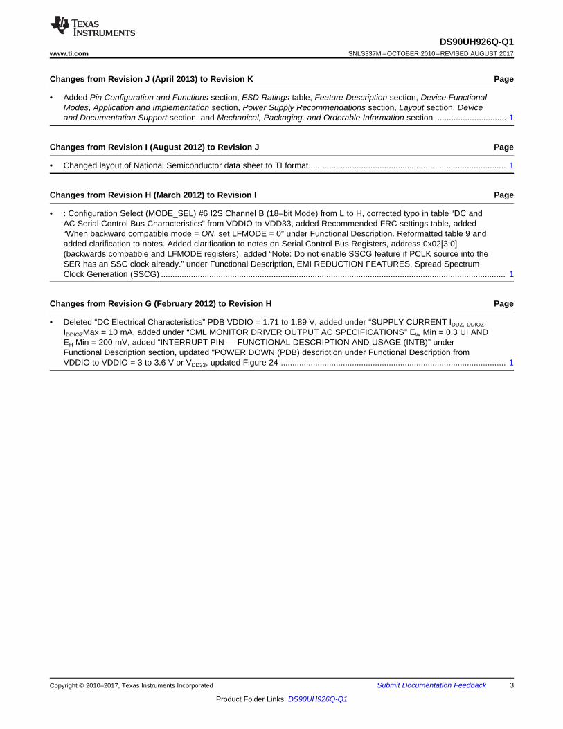
R[7:0] HS VS PCLK PDB Serializer Deserializer DE RGB Display 720p 24-bit color depth RGB Digital Display Interface HOST Graphics Processor FPD-Link III 1 Pair / AC Coupled DS90UH925Q DS90UH926Q 100 ohm STP Cable PA SS VDDIO OS S_SE L SCL SDA INTB I2S AUDI O (STEREO) OE N LO CK IDx DAP DAP 0.1 PF 0.1 PF G[7:0] B[7:0] SCL SDA IDx R[7:0] HS VS PCLK DE G[7:0] B[7:0] RIN+ RIN- DOUT+ DOUT- (1.8V or 3.3V) (1.8V or 3.3V) (3.3V) (3.3V) VDDIO 3 / I2S AUDI O (STEREO) 3 / MODE_SEL MODE_SEL PDB INTB_IN VDD33 VDD33 MCLK 0.1 PF 0.1 PF Product Folder Order Now Technical Documents Tools & Software Support & Community Reference Design An IMPORTANT NOTICE at the end of this data sheet addresses availability, warranty, changes, use in safety-critical applications, intellectual property matters and other important disclaimers. PRODUCTION DATA. DS90UH926Q-Q1 SNLS337M – OCTOBER 2010 – REVISED AUGUST 2017 DS90UH926Q-Q1 720p, 24-Bit Color FPD-Link III Deserializer With HDCP 1 1 Features 1• AEC-Q100 Qualified for Automotive Applications – Device Temperature Grade 2: –40°C to +105°C Ambient Operating Temperature – Device HBM ESD Classification Level 3B – Device CDM ESD Classification Level C6 – Device MM ESD Classification Level M3 • Integrated HDCP Cipher Engine With On-Chip Key Storage • Bidirectional Control Interface Channel Interface With I 2 C Compatible Serial Control Bus • Supports High-Definition (720p) Digital Video Format • RGB888 + VS, HS, DE and I2S Audio Supported • 5- to 85-MHz PCLK Supported • Single 3.3-V Operation With 1.8-V or 3.3-V Compatible LVCMOS I/O Interface • AC-Coupled STP Interconnect up to 10 Meters • Parallel LVCMOS Video Outputs • DC-Balanced and Scrambled Data With Embedded Clock • Adaptive Cable Equalization • Supports HDCP Repeater Application • Image Enhancement (White Balance and Dithering) and Internal Pattern Generation • EMI Minimization (SSCG and EPTO) • Low Power Modes Minimize Power Dissipation • Backward-Compatible Modes 2 Applications • Automotive Display for Navigation • Rear Seat Entertainment Systems 3 Description The DS90UH926Q-Q1 deserializer, in conjunction with the DS90UH925Q-Q1 serializer, provides a solution for secure distribution of content-protected digital video within automotive entertainment systems. This chipset translates a parallel RGB video interface into a single-pair high-speed serialized interface. The digital video data is protected using the industry standard HDCP copy protection scheme. The serial bus scheme, FPD-Link III, supports full duplex of high-speed forward data transmission and low-speed backchannel communication over a single differential link. Consolidation of video data and control over a single differential pair reduces the interconnect size and weight, while also eliminating skew issues and simplifying system design. The DS90UH926Q-Q1 deserializer has a 31-bit parallel LVCMOS output interface to accommodate the RGB, video control, and audio data. The device extracts the clock from a high-speed serial stream. An output LOCK pin provides the link status if the incoming data stream is locked, without the use of a training sequence or special SYNC patterns, as well as a reference clock. An adaptive equalizer optimizes the maximum cable reach. EMI is minimized by output SSC generation (SSCG) and enhanced progressive turnon (EPTO) features. The HDCP cipher engine is implemented in both the serializer and deserializer. HDCP keys are stored in on-chip memory. Device Information (1) PART NUMBER PACKAGE BODY SIZE (NOM) DS90UH926Q-Q1 WQFN (60) 9.00 mm × 9.00 mm (1) For all available packages, see the orderable addendum at the end of the data sheet. Application Diagram
Transcript
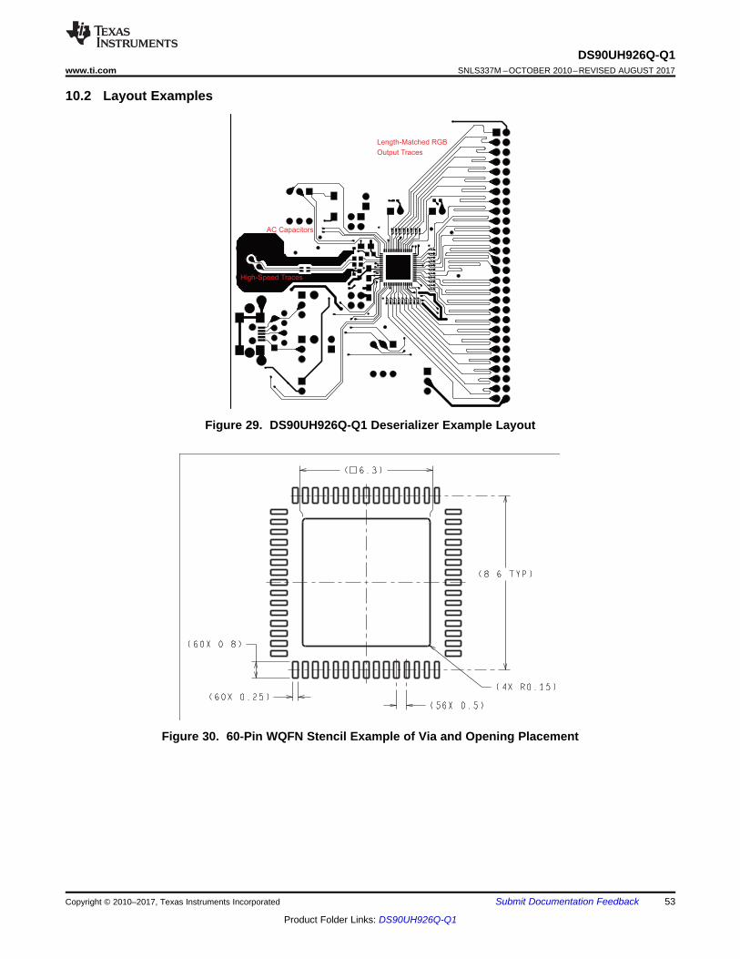
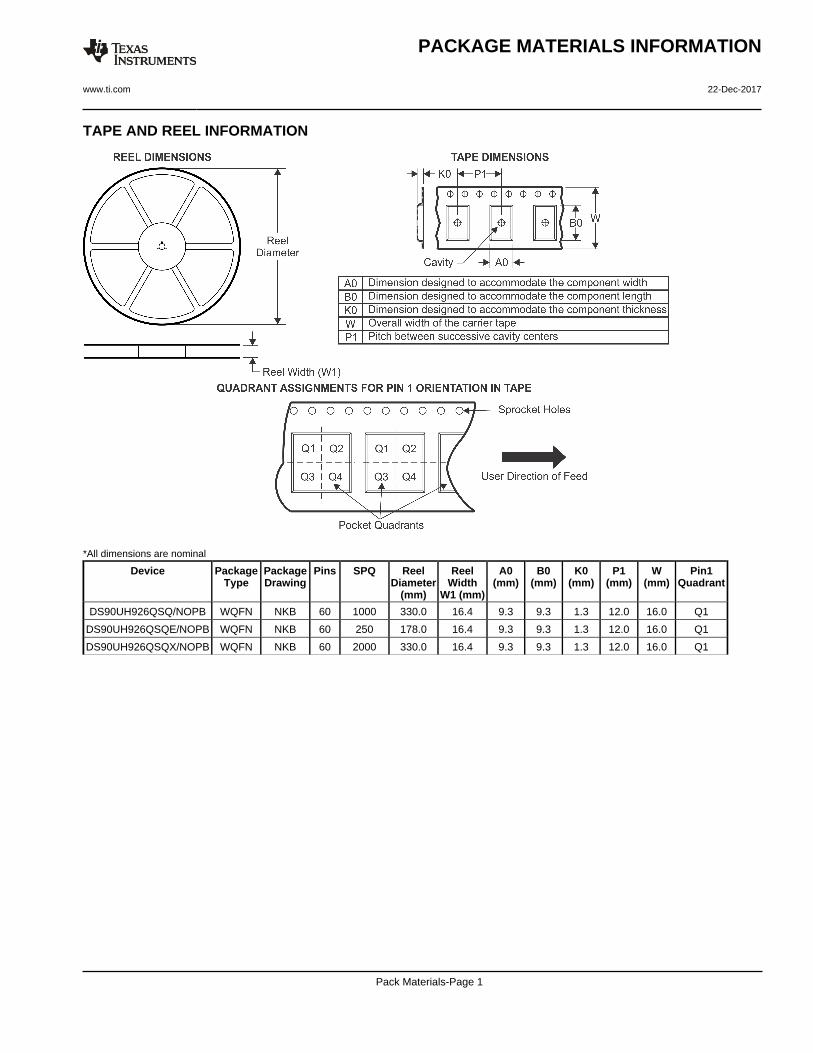
R[7:0]
HSVS
PCLK
PDBSerializer Deserializer
DE
RGB Display720p
24-bit color depth
RG
B D
igita
l Dis
play
Int
erf
ace
HOSTGraphicsProcessor
FPD-Link III1 Pair / AC Coupled
DS90UH925Q DS90UH926Q100 ohm STP Cable
PASS
VDDIO
OSS_SEL
SCLSDA
INTB
I2S AUDIO (STEREO)
OEN
LOCK
IDx DAP DAP
0.1 PF 0.1 PF
G[7:0]B[7:0]
SCLSDAIDx
R[7:0]
HSVS
PCLKDE
G[7:0]B[7:0]
RIN+
RIN-
DOUT+
DOUT-
(1.8V or 3.3V)(1.8V or 3.3V) (3.3V) (3.3V)VDDIO
3/
I2S AUDIO (STEREO)
3/MODE_SEL MODE_SEL
PDB
INTB_IN
VDD33 VDD33
MCLK
0.1 PF 0.1 PF
Product
Folder
Order
Now
Technical
Documents
Tools &
Software
Support &Community
ReferenceDesign
An IMPORTANT NOTICE at the end of this data sheet addresses availability, warranty, changes, use in safety-critical applications,intellectual property matters and other important disclaimers. PRODUCTION DATA.
DS90UH926Q-Q1SNLS337M –OCTOBER 2010–REVISED AUGUST 2017
DS90UH926Q-Q1 720p, 24-Bit Color FPD-Link III Deserializer With HDCP
1
1 Features1• AEC-Q100 Qualified for Automotive Applications
– Device Temperature Grade 2: –40°C to+105°C Ambient Operating Temperature
Dithering) and Internal Pattern Generation• EMI Minimization (SSCG and EPTO)• Low Power Modes Minimize Power Dissipation• Backward-Compatible Modes
2 Applications• Automotive Display for Navigation• Rear Seat Entertainment Systems
3 DescriptionThe DS90UH926Q-Q1 deserializer, in conjunctionwith the DS90UH925Q-Q1 serializer, provides asolution for secure distribution of content-protecteddigital video within automotive entertainmentsystems. This chipset translates a parallel RGB videointerface into a single-pair high-speed serializedinterface. The digital video data is protected using theindustry standard HDCP copy protection scheme.The serial bus scheme, FPD-Link III, supports fullduplex of high-speed forward data transmission andlow-speed backchannel communication over a singledifferential link. Consolidation of video data andcontrol over a single differential pair reduces theinterconnect size and weight, while also eliminatingskew issues and simplifying system design.
The DS90UH926Q-Q1 deserializer has a 31-bitparallel LVCMOS output interface to accommodatethe RGB, video control, and audio data. The deviceextracts the clock from a high-speed serial stream.An output LOCK pin provides the link status if theincoming data stream is locked, without the use of atraining sequence or special SYNC patterns, as wellas a reference clock.
An adaptive equalizer optimizes the maximum cablereach. EMI is minimized by output SSC generation(SSCG) and enhanced progressive turnon (EPTO)features.
The HDCP cipher engine is implemented in both theserializer and deserializer. HDCP keys are stored inon-chip memory.
Device Information(1)
PART NUMBER PACKAGE BODY SIZE (NOM)DS90UH926Q-Q1 WQFN (60) 9.00 mm × 9.00 mm
(1) For all available packages, see the orderable addendum atthe end of the data sheet.
Table of Contents1 Features .................................................................. 12 Applications ........................................................... 13 Description ............................................................. 14 Revision History..................................................... 25 Pin Configuration and Functions ......................... 46 Specifications......................................................... 7
6.1 Absolute Maximum Ratings ..................................... 76.2 ESD Ratings.............................................................. 76.3 Recommended Operating Conditions....................... 76.4 Thermal Information .................................................. 86.5 DC Electrical Characteristics .................................... 86.6 AC Electrical Characteristics................................... 106.7 DC and AC Serial Control Bus Characteristics....... 106.8 Recommended Timing Requirements for the Serial
Control Bus .............................................................. 116.9 Switching Characteristics ........................................ 116.10 Timing Diagrams................................................... 126.11 Typical Characteristics .......................................... 15
11 Device and Documentation Support ................. 5411.1 Documentation Support ........................................ 5411.2 Receiving Notification of Documentation Updates 5411.3 Community Resources.......................................... 5411.4 Trademarks ........................................................... 5411.5 Electrostatic Discharge Caution............................ 5411.6 Glossary ................................................................ 54
12 Mechanical, Packaging, and OrderableInformation ........................................................... 54
4 Revision HistoryNOTE: Page numbers for previous revisions may differ from page numbers in the current version.
Changes from Revision L (February 2017) to Revision M Page
• Reverted all previous MLCK content changes made in Revision L back to Revision K ........................................................ 1• Removed disable jitter cleaner note ....................................................................................................................................... 5
Changes from Revision K (January 2015) to Revision L Page
• Changed top view pin out diagram ........................................................................................................................................ 4• Changed CLK to RES2 .......................................................................................................................................................... 5• Added note to disable jitter cleaner ....................................................................................................................................... 5• Changed MCLK to RES2 ....................................................................................................................................................... 5• Deleted reference to MCLK in this section ............................................................................................................................ 8• Deleted reference to MCLK in this section .......................................................................................................................... 11• Deleted reference to MCLK ................................................................................................................................................. 25• Deleted I2S Jitter Cleaning section ..................................................................................................................................... 25• Deleted MCLK section ......................................................................................................................................................... 25• Deleted MCLK columns in the Audio Interface Frequencies table....................................................................................... 26• Changed values in columns 2 to 5 of Configuration Select (MODE_SEL) table.................................................................. 29• Changed values in columns 2 to 5 of IDx table ................................................................................................................... 32• Changed Removed register reference to MCLK .................................................................................................................. 42• Changed Typical Display System Diagram (removed MCLK) ............................................................................................. 47• Changed Power-Up Requirements and PDB pin description and added Power-Up Sequence graphic. ........................... 50
Changes from Revision J (April 2013) to Revision K Page
• Added Pin Configuration and Functions section, ESD Ratings table, Feature Description section, Device FunctionalModes, Application and Implementation section, Power Supply Recommendations section, Layout section, Deviceand Documentation Support section, and Mechanical, Packaging, and Orderable Information section .............................. 1
Changes from Revision I (August 2012) to Revision J Page
• Changed layout of National Semiconductor data sheet to TI format...................................................................................... 1
Changes from Revision H (March 2012) to Revision I Page
• : Configuration Select (MODE_SEL) #6 I2S Channel B (18–bit Mode) from L to H, corrected typo in table “DC andAC Serial Control Bus Characteristics” from VDDIO to VDD33, added Recommended FRC settings table, added“When backward compatible mode = ON, set LFMODE = 0” under Functional Description. Reformatted table 9 andadded clarification to notes. Added clarification to notes on Serial Control Bus Registers, address 0x02[3:0](backwards compatible and LFMODE registers), added “Note: Do not enable SSCG feature if PCLK source into theSER has an SSC clock already.” under Functional Description, EMI REDUCTION FEATURES, Spread SpectrumClock Generation (SSCG) ...................................................................................................................................................... 1
Changes from Revision G (February 2012) to Revision H Page
• Deleted “DC Electrical Characteristics” PDB VDDIO = 1.71 to 1.89 V, added under “SUPPLY CURRENT IDDZ, DDIOZ,IDDIOZMax = 10 mA, added under “CML MONITOR DRIVER OUTPUT AC SPECIFICATIONS” EW Min = 0.3 UI ANDEH Min = 200 mV, added “INTERRUPT PIN — FUNCTIONAL DESCRIPTION AND USAGE (INTB)” underFunctional Description section, updated "POWER DOWN (PDB) description under Functional Description fromVDDIO to VDDIO = 3 to 3.6 V or VDD33, updated Figure 24 .................................................................................................. 1
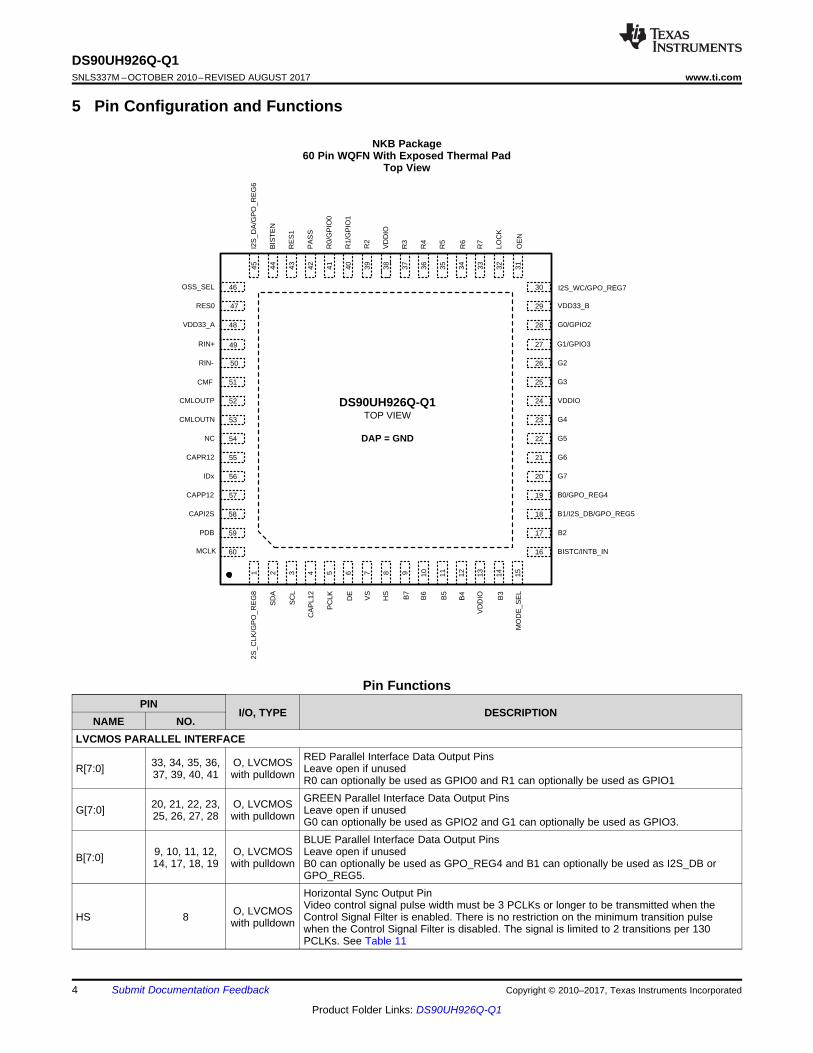
RED Parallel Interface Data Output PinsLeave open if unusedR0 can optionally be used as GPIO0 and R1 can optionally be used as GPIO1
G[7:0] 20, 21, 22, 23,25, 26, 27, 28
O, LVCMOSwith pulldown
GREEN Parallel Interface Data Output PinsLeave open if unusedG0 can optionally be used as GPIO2 and G1 can optionally be used as GPIO3.
B[7:0] 9, 10, 11, 12,14, 17, 18, 19
O, LVCMOSwith pulldown
BLUE Parallel Interface Data Output PinsLeave open if unusedB0 can optionally be used as GPO_REG4 and B1 can optionally be used as I2S_DB orGPO_REG5.
HS 8 O, LVCMOSwith pulldown
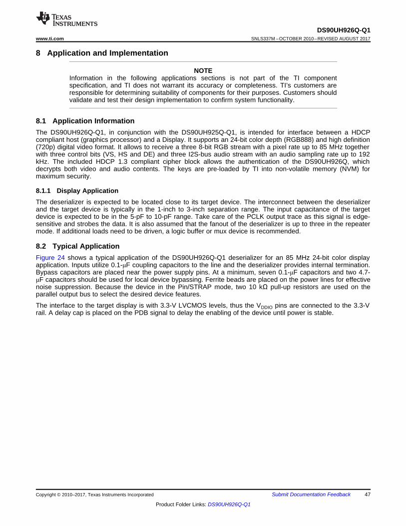
Horizontal Sync Output PinVideo control signal pulse width must be 3 PCLKs or longer to be transmitted when theControl Signal Filter is enabled. There is no restriction on the minimum transition pulsewhen the Control Signal Filter is disabled. The signal is limited to 2 transitions per 130PCLKs. See Table 11
Vertical Sync Output PinVideo control signal is limited to 1 transition per 130 PCLKs. Thus, the minimum pulsewidth is 130 PCLKs.
DE 6 O, LVCMOSwith pulldown
Data Enable Output PinVideo control signal pulse width must be 3 PCLKs or longer to be transmitted when theControl Signal Filter is enabled. There is no restriction on the minimum transition pulsewhen the Control Signal Filter is disabled. The signal is limited to 2 transitions per 130PCLKs. See Table 11
PCLK 5 O, LVCMOSwith pulldown Pixel Clock Output Pin. Strobe edge set by RFB configuration register. See Table 11
I2S_CLK,I2S_WC,I2S_DA
1, 30, 45 O, LVCMOSwith pulldown
Digital Audio Interface Data Output PinsLeave open if unusedI2S_CLK can optionally be used as GPO_REG8, I2S_WC can optionally be used asGPO_REG7, and I2S_DA can optionally be used as GPO_REG6.
MCLK 60 O, LVCMOSwith pulldown
I2S Master Clock Outputx1, x2, or x4 of I2S_CLK Frequency
OPTIONAL PARALLEL INTERFACE
I2S_DB 18 O, LVCMOSwith pulldown
Second Channel Digital Audio Interface Data Output pin at 18–bit color mode and set byMODE_SEL or configuration registerLeave open if unusedI2S_B can optionally be used as BI or GPO_REG5.
GPIO[3:0] 27, 28, 40, 41 I/O, LVCMOSwith pulldown
Standard General Purpose IOs.Available only in 18-bit color mode, and set by MODE_SEL or configuration register.See Table 11Leave open if unusedShared with G1, G0, R1 and R0.
GPO_REG[8:4]
1, 30, 45, 18,19
O, LVCMOSwith pulldown
General Purpose Outputs and set by configuration register. See Table 11Shared with I2S_CLK, I2S_WC, I2S_DA, I2S_DB or B1, B0.
INTB_IN 16Input,
LVCMOSwith pulldown
Interrupt InputShared with BISTC
CONTROL
PDB 59 I, LVCMOSwith pulldown
Power-down Mode Input PinPDB = H, device is enabled (normal operation)Refer to Power Supply Recommendations.PDB = L, device is powered down.When the device is in the POWER DOWN state, the LVCMOS Outputs are in TRI-STATE,the PLL is shutdown and IDD is minimized.
OEN 31Input,
LVCMOSwith pulldown
Output Enable Pin.See Table 8
OSS_SEL 46Input,
LVCMOSwith pulldown
Output Sleep State Select Pin.See Table 8
MODE_SEL 15 I, Analog Device Configuration Select. See Table 9
BISTEN 44 I, LVCMOSwith pulldown
BIST Enable Pin.0: BIST Mode is disabled.1: BIST Mode is enabled.
BISTC 16 I, LVCMOSwith pulldown
BIST Clock Select.Shared with INTB_IN0: PCLK; 1: 33 MHz
(1) The VDD (VDD33 and VDDIO) supply ramp should be faster than 1.5 ms with a monotonic rise.
I2C
IDx 56 I, Analog
I2C Serial Control Bus Device ID Address SelectExternal pull-up to VDD33 is required under all conditions, DO NOT FLOAT.Connect to external pullup and pulldown resistor to create a voltage divider.See Figure 23
SCL 3 I/O, LVCMOSOpen-Drain
I2C Clock Input / Output InterfaceMust have an external pullup to VDD33, DO NOT FLOAT.Recommended pullup: 4.7 kΩ.
SDA 2 I/O, LVCMOSOpen-Drain
I2C Data Input / Output InterfaceMust have an external pullup to VDD33, DO NOT FLOAT.Recommended pullup: 4.7 kΩ.
STATUS
LOCK 32 O, LVCMOSwith pulldown
LOCK Status Output Pin0: PLL is unlocked, RGB[7:0], I2S[2:0], HS, VS, DE and PCLK output states are controlledby OEN. May be used as Link Status or Display Enable1: PLL is Locked, outputs are active
PASS 42 O, LVCMOSwith pulldown
PASS Output Pin0: One or more errors were detected in the received payload1: ERROR FREE TransmissionLeave Open if unused. Route to test point (pad) recommended
FPD-LINK III SERIAL INTERFACE
RIN+ 49 I, LVDS True Input.The interconnection should be AC-coupled to this pin with a 0.1 μF capacitor.
RIN– 50 I, LVDS Inverting Input.The interconnection should be AC-coupled to this pin with a 0.1 μF capacitor.
CMLOUTP 52 O, LVDS True CML OutputMonitor point for equalized differential signal
CMLOUTN 53 O, LVDS Inverting CML OutputMonitor point for equalized differential signal
CMF 51 Analog Common Mode Filter. Connect 0.1-μF capacitor to GND.POWER (1) AND GROUNDVDD33_A,VDD33_B 48, 29 Power Power to on-chip regulator 3 V – 3.6 V. Requires 4.7 uF to GND at each VDD pin.
VDDIO 13, 24, 38 Power LVCMOS I/O Power 1.8 V ±5% OR 3 V – 3.6 V. Requires 4.7 uF to GND at each VDDIOpin.
GND DAP Ground DAP is the large metal contact at the bottom side, located at the center of the WQFNpackage. Connect to the ground plane (GND) with at least 9 vias.
REGULATOR CAPACITORCAPR12 55
CAP Decoupling capacitor connection for on-chip regulator. Requires a 4.7-µF to GND at eachCAP pin.CAPP12 57
CAPI2S 58
CAPL12 4 CAP Decoupling capacitor connection for on-chip regulator. Requires two 4.7-µF to GND at thisCAP pin.
OTHERSNC 54 NC No connect. This pin may be left open or tied to any level.RES[1:0] 43.47 GND Reserved - tie to Ground
(1) Stresses beyond those listed under Absolute Maximum Ratings may cause permanent damage to the device. These are stress ratingsonly, which do not imply functional operation of the device at these or any other conditions beyond those indicated under RecommendedOperating Conditions. Exposure to absolute-maximum-rated conditions for extended periods may affect device reliability.
(2) If Military/Aerospace specified devices are required, contact the Texas Instruments Sales Office/ Distributors for availability andspecifications.
(3) For soldering specifications, see product folder at www.ti.com and Absolute Maximum Ratings for Soldering (SNOA549).
6 Specifications
6.1 Absolute Maximum RatingsSee (1) (2) (3)
MIN MAX UNITSupply voltage – VDD33 −0.3 4 VSupply voltage – VDDIO −0.3 4 VLVCMOS I/O voltage −0.3 (VDDIO + 0.3) VDeserializer input voltage −0.3 2.75 VJunction temperature 150 °C60-pin WQFN PackageMaximum power dissipationcapacity at 25°C
(1) AEC Q100-002 indicates that HBM stressing shall be in accordance with the ANSI/ESDA/JEDEC JS-001 specification.
6.2 ESD RatingsVALUE UNIT
V(ESD)Electrostaticdischarge
Human-body model (HBM), per AEC Q100-002 (1) ±8000
V
Charged-device model (CDM), per AEC Q100-011 ±1250Machine model, all pins ±250
(IEC, powered-up only)RD = 330 Ω, CS = 150 pF
Air Discharge (Pin 49 and 50) ±15000Contact Discharge (Pin 49 and 50) ±8000
(ISO10605)RD = 330 Ω, CS = 150 pF
Air Discharge (Pin 49 and 50) ±15000Contact Discharge (Pin 49 and 50) ±8000
(ISO10605)RD = 2 kΩ, CS = 150 & 330 pF
Air Discharge (Pin 49 and 50) ±15000Contact Discharge (Pin 49 and 50) ±8000
(1) Supply noise testing was done with minimum capacitors on the PCB. A sinusoidal signal is AC-coupled to the VDD33 and VDDIO supplieswith amplitude = 100 mVp-p measured at the device VDD33 and VDDIO pins. Bit error rate testing of input to the Ser and output of theDes with 10-meter cable shows no error when the noise frequency on the Ser is less than 50 MHz. The Des on the other hand showsno error when the noise frequency is less than 50 MHz.
6.3 Recommended Operating ConditionsMIN NOM MAX UNIT
Supply voltage (VDD33) 3 3.3 3.6 VLVCMOS supply voltage (VDDIO) Connect VDDIO to 3.3 V and use 3.3-V IOs 3 3.3 3.6 V
Connect VDDIO to 1.8 V and use 1.8-V IOs 1.71 1.8 1.89 VOperating free air temperature (TA) −40 25 105 °CPCLK frequency 5 85 MHzSupply noise (1) 100 mVP-P
(1) The Electrical Characteristics tables list ensured specifications under the listed Recommended Operating Conditions except asotherwise modified or specified by the electrical characteristics conditions and/or notes. Typical specifications are estimations only andare not ensured.
(2) Typical values represent most likely parametric norms at VDD = 3.3 V, TA = 25 °C, and at Recommended Operating Conditions at thetime of product characterization and are not ensured.
(3) Current into device pins is defined as positive. Current out of a device pin is defined as negative. Voltages are referenced to groundexcept VOD and ΔVOD, which are differential voltages.
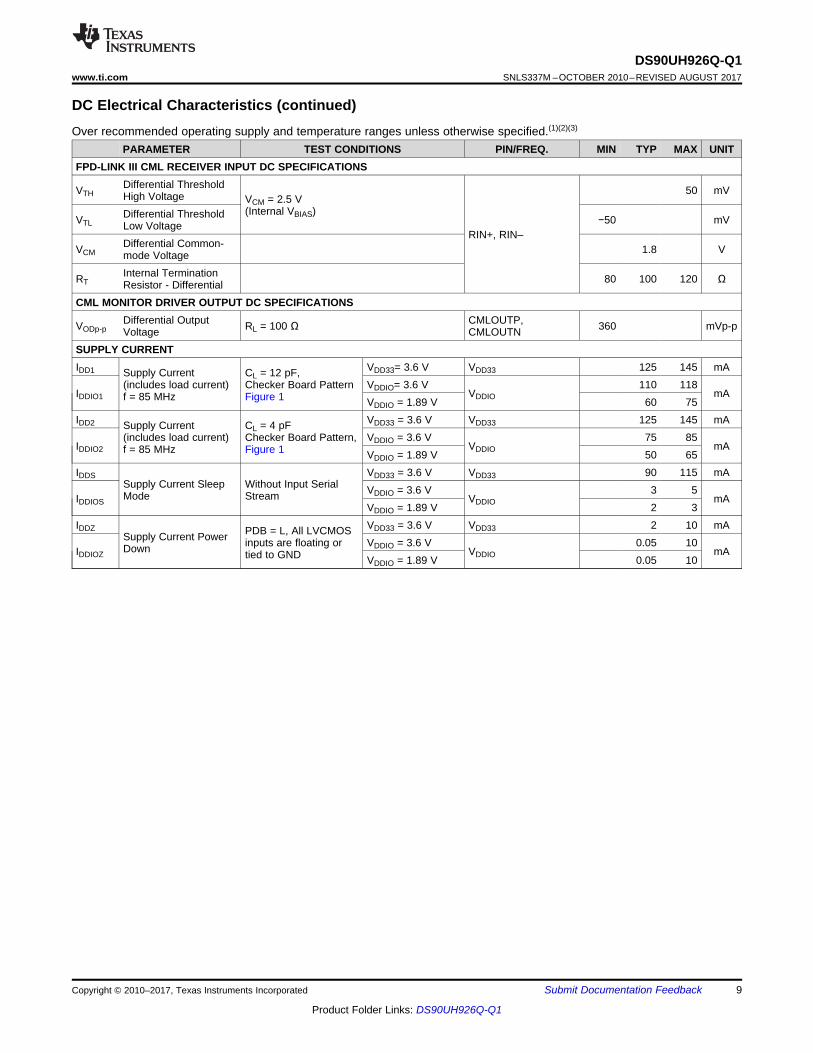
6.5 DC Electrical CharacteristicsOver recommended operating supply and temperature ranges unless otherwise specified. (1) (2) (3)
PARAMETER TEST CONDITIONS PIN/FREQ. MIN TYP MAX UNITLVCMOS I/O DC SPECIFICATIONS
VIHHigh Level InputVoltage VDDIO = 3 to 3.6 V
PDB
2 VDDIO V
VILLow Level InputVoltage VDDIO = 3 to 3.6 V GND 0.8 V
IIN Input Current VIN = 0 V or VDDIO = 3 to 3.6 V −10 ±1 10 μA
VIHHigh Level InputVoltage
VDDIO = 3 to 3.6 V
OEN, OSS_SEL,BISTEN, BISTC /INTB_IN, GPIO[3:0]
2 VDDIO V
VDDIO = 1.71 to 1.89 V 0.65 ×VDDIO
VDDIO V
VILLow Level InputVoltage
VDDIO = 3 to 3.6 V GND 0.8 V
VDDIO = 1.71 to 1.89 V GND 0.35 ×VDDIO
V
IIN Input Current VIN = 0 V or VDDIO
VDDIO = 3to 3.6 V −10 ±1 10 μA
VDDIO = 1.7to 1.89 V −10 ±1 10 μA
VOHHigh Level OutputVoltage IOH = −4 mA
VDDIO = 3 to 3.6 V
R[7:0], G[7:0], B[7:0],HS, VS, DE, PCLK,LOCK, PASS, MCLK,I2S_CLK, I2S_WC,I2S_DA, I2S_DB,GPO_REG[8:4]
2.4 VDDIO VVDDIO = 1.7to 1.89 V
VDDIO-0.45 VDDIO V
VOLLow Level OutputVoltage IOL = 4 mA
VDDIO = 3 to 3.6 V GND 0.4 VVDDIO = 1.7to 1.89 V GND 0.35 V
IOSOutput Short-CircuitCurrent VOUT = 0 V −60 mA
IOZ Tri-state Output Current VOUT = 0 V or VDDIO, PDB = L −10 10 μA
(1) The Electrical Characteristics tables list ensured specifications under the listed Recommended Operating Conditions except asotherwise modified or specified by the electrical characteristics conditions and/or notes. Typical specifications are estimations only andare not ensured.
(2) Typical values represent most likely parametric norms at VDD = 3.3 V, TA = 25 °C, and at Recommended Operating Conditions at thetime of product characterization and are not ensured.
(3) Current into device pins is defined as positive. Current out of a device pin is defined as negative. Voltages are referenced to groundexcept VOD and ΔVOD, which are differential voltages.
(4) Specification is ensured by characterization and is not tested in production.(5) Specification is ensured by design and is not tested in production.(6) UI – Unit Interval is equivalent to one serialized data bit width (1UI = 1 / 35 × PCLK). The UI scales with PCLK frequency.
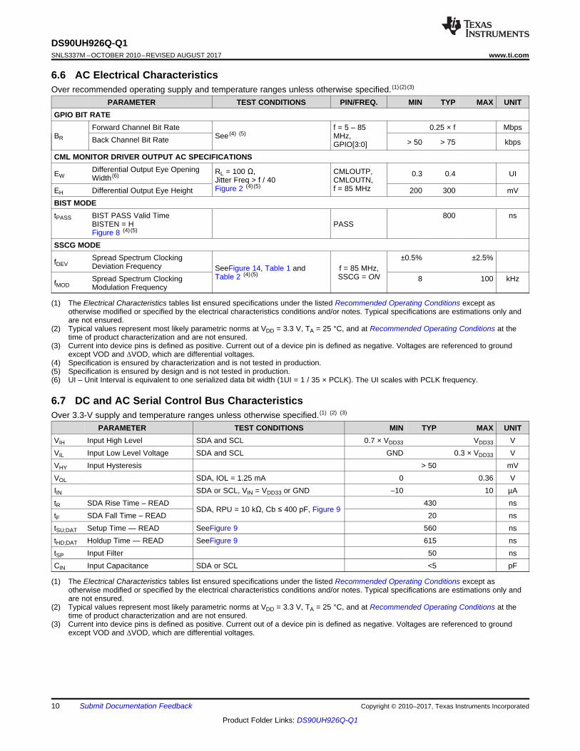
6.6 AC Electrical CharacteristicsOver recommended operating supply and temperature ranges unless otherwise specified. (1) (2) (3)
PARAMETER TEST CONDITIONS PIN/FREQ. MIN TYP MAX UNITGPIO BIT RATE
fDEVSpread Spectrum ClockingDeviation Frequency SeeFigure 14, Table 1 and
Table 2 (4) (5)f = 85 MHz,SSCG = ON
±0.5% ±2.5%
fMODSpread Spectrum ClockingModulation Frequency
8 100 kHz
(1) The Electrical Characteristics tables list ensured specifications under the listed Recommended Operating Conditions except asotherwise modified or specified by the electrical characteristics conditions and/or notes. Typical specifications are estimations only andare not ensured.
(2) Typical values represent most likely parametric norms at VDD = 3.3 V, TA = 25 °C, and at Recommended Operating Conditions at thetime of product characterization and are not ensured.
(3) Current into device pins is defined as positive. Current out of a device pin is defined as negative. Voltages are referenced to groundexcept VOD and ΔVOD, which are differential voltages.
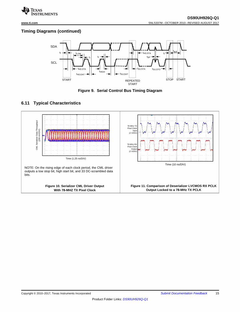
6.7 DC and AC Serial Control Bus CharacteristicsOver 3.3-V supply and temperature ranges unless otherwise specified. (1) (2) (3)
PARAMETER TEST CONDITIONS MIN TYP MAX UNITVIH Input High Level SDA and SCL 0.7 × VDD33 VDD33 VVIL Input Low Level Voltage SDA and SCL GND 0.3 × VDD33 VVHY Input Hysteresis > 50 mVVOL SDA, IOL = 1.25 mA 0 0.36 VIIN SDA or SCL, VIN = VDD33 or GND –10 10 µAtR SDA Rise Time – READ
SDA, RPU = 10 kΩ, Cb ≤ 400 pF, Figure 9430 ns
tF SDA Fall Time – READ 20 nstSU;DAT Setup Time — READ SeeFigure 9 560 nstHD;DAT Holdup Time — READ SeeFigure 9 615 nstSP Input Filter 50 nsCIN Input Capacitance SDA or SCL <5 pF
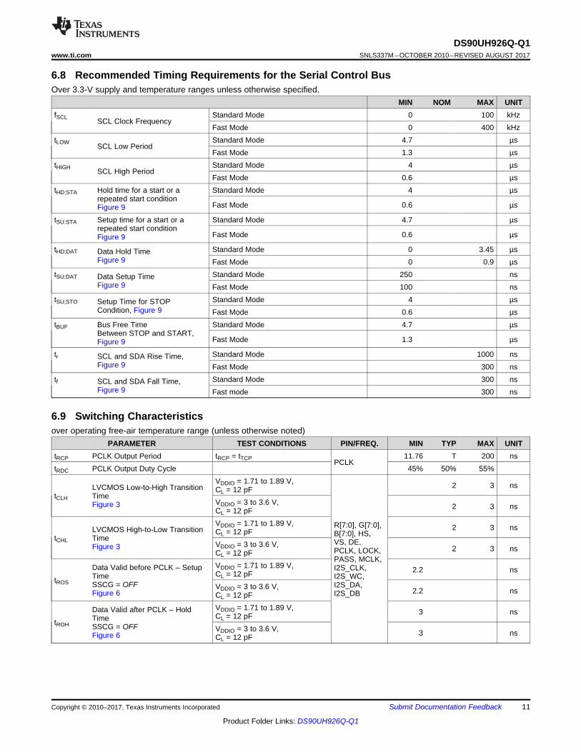
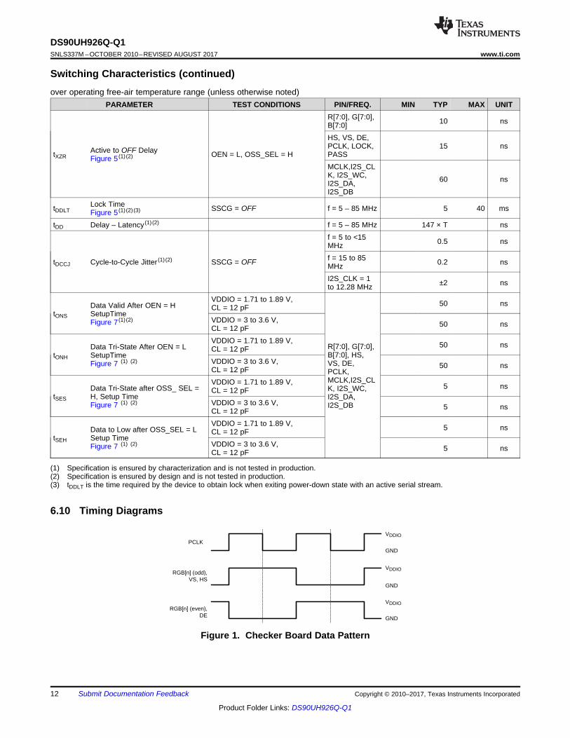
Switching Characteristics (continued)over operating free-air temperature range (unless otherwise noted)
PARAMETER TEST CONDITIONS PIN/FREQ. MIN TYP MAX UNIT
(1) Specification is ensured by characterization and is not tested in production.(2) Specification is ensured by design and is not tested in production.(3) tDDLT is the time required by the device to obtain lock when exiting power-down state with an active serial stream.
tXZRActive to OFF DelayFigure 5 (1) (2) OEN = L, OSS_SEL = H
R[7:0], G[7:0],B[7:0] 10 ns
HS, VS, DE,PCLK, LOCK,PASS
15 ns
MCLK,I2S_CLK, I2S_WC,I2S_DA,I2S_DB
60 ns
tDDLTLock TimeFigure 5 (1) (2) (3) SSCG = OFF f = 5 – 85 MHz 5 40 ms
tDD Delay – Latency (1) (2) f = 5 – 85 MHz 147 × T ns
7.1 OverviewThe DS90UH926Q-Q1 deserializer receives a 35 bits symbol over a single serial FPD-Link III pair operating up toa 2.975 Gbps application payload. The serial stream contains an embedded clock, video control signals and theDC-balanced video data and audio data which enhance signal quality to support AC coupling.
The DS90UH926Q-Q1 deserializer attains lock to a data stream without the use of a separate reference clocksource, which greatly simplifies system complexity and overall cost. The deserializer also synchronizes to theserializer regardless of the data pattern, delivering true automatic plug and lock performance. It can lock to theincoming serial stream without the need of special training patterns or sync characters. The deserializer recoversthe clock and data by extracting the embedded clock information, validating then deserializing the incoming datastream. It also applies decryption through a High-Bandwidth Digital Content Protection (HDCP) Cipher to thisvideo and audio data stream following reception of the data from the FPD-Link III decoder. The decrypted parallelLVCMOS video bus is provided to the display. The deserializer is intended for use with the DS90UH925Qserializer, but is also backward-compatible with DS90UR905Q or DS90UR907Q FPD-Link II serializer.
7.2 Functional Block Diagram
7.3 Feature Description
7.3.1 High-Speed Forward Channel Data TransferThe high-speed forward channel (HS_FC) is composed of 35 bits of data containing RGB data, sync signals,HDCP, I2C, and I2S audio transmitted from Serializer to Deserializer. Figure 12 illustrates the serial stream perPCLK cycle. This data payload is optimized for signal transmission over an AC-coupled link. Data is randomized,balanced and scrambled.
Feature Description (continued)The device supports clocks in the range of 5 MHz to 85 MHz. The application payload rate is 2.975-Gbpsmaximum (175 Mbps minimum) with the actual line rate of 2.975 Gbps maximum and 525 Mbps minimum.
7.3.2 Low-Speed Back Channel Data TransferThe low-speed backward channel (LS_BC) of the DS90UH926Q-Q1 provides bidirectional communicationbetween the display and host processor. The information is carried back from the Deserializer to the Serializerper serial symbol. The back channel control data is transferred over the single serial link along with the high-speed forward data, DC balance coding, and embedded clock information. This architecture provides a backwardpath across the serial link together with a high-speed forward channel. The back channel contains the I2C,HDCP, CRC and 4 bits of standard GPIO information with 10-Mbps line rate.
7.3.3 Backward Compatible ModeThe DS90UH926Q-Q1 is also backward-compatible to DS90UR905Q and DS90UR907Q FPD Link II serializerswith 15- to 65-MHz pixel clock frequencies supported. It receives 28 bits of data over a single serial FPD-Link IIpair operating at the line rate of 420 Mbps to 1.82 Gbps. This backward-compatible mode is provided through theMODE_SEL pin (Table 9) or the configuration register (Table 11). When backward-compatible mode = ON, setLFMODE = 0.
7.3.4 Input Equalization GainFPD-Link III input adaptive equalizer provides compensation for transmission medium losses and reduces themedium-induced deterministic jitter. It equalizes up to 10 meter STP cables with 3 connection breaks atmaximum serialized stream payload rate of 2.975 Gbps.
7.3.5 Common-Mode Filter Pin (CMF)The deserializer provides access to the center tap of the internal termination. A capacitor must be placed on thispin for additional common-mode filtering of the differential pair. This can be useful in high noise environments foradditional noise rejection capability. A 0.1-μF capacitor has to be connected to this pin to Ground.
7.3.6 Video Control Signal FilterWhen operating the devices in Normal Mode, the Video Control Signals (DE, HS, VS) have the followingrestrictions:• Normal Mode with Control Signal Filter Enabled: DE and HS — Only 2 transitions per 130 clock cycles are
transmitted, the transition pulse must be 3 PCLK or longer.• Normal Mode with Control Signal Filter Disabled: DE and HS — Only 2 transitions per 130 clock cycles are
transmitted, no restriction on minimum transition pulse.• VS — Only 1 transition per 130 clock cycles are transmitted, minimum pulse width is 130 clock cycles.
Video Control Signals are defined as low-frequency signals with limited transitions. Glitches of a control signalcan cause a visual display error. This feature allows for the chipset to validate and filter out any high-frequencynoise on the control signals. See Figure 13.
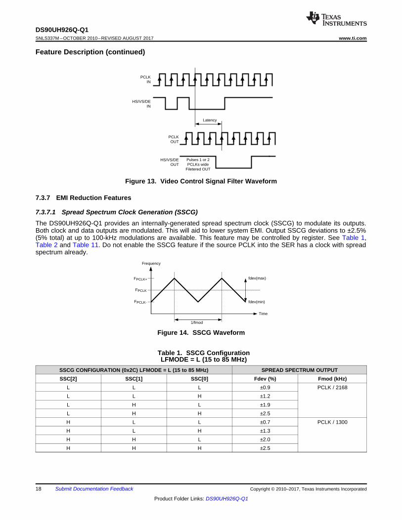
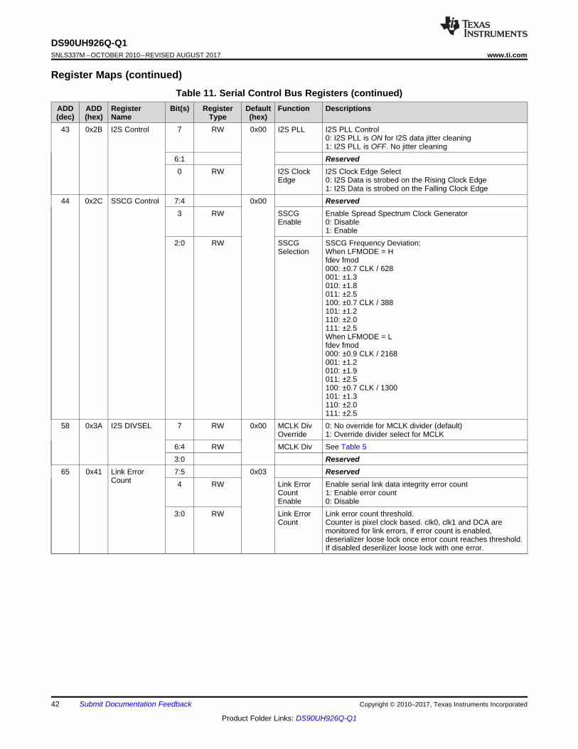
7.3.7.1 Spread Spectrum Clock Generation (SSCG)The DS90UH926Q-Q1 provides an internally-generated spread spectrum clock (SSCG) to modulate its outputs.Both clock and data outputs are modulated. This will aid to lower system EMI. Output SSCG deviations to ±2.5%(5% total) at up to 100-kHz modulations are available. This feature may be controlled by register. See Table 1,Table 2 and Table 11. Do not enable the SSCG feature if the source PCLK into the SER has a clock with spreadspectrum already.
Figure 14. SSCG Waveform
Table 1. SSCG ConfigurationLFMODE = L (15 to 85 MHz)
SSCG CONFIGURATION (0x2C) LFMODE = L (15 to 85 MHz) SPREAD SPECTRUM OUTPUTSSC[2] SSC[1] SSC[0] Fdev (%) Fmod (kHz)
L L L ±0.9 PCLK / 2168L L H ±1.2L H L ±1.9L H H ±2.5H L L ±0.7 PCLK / 1300H L H ±1.3H H L ±2.0H H H ±2.5
Table 2. SSCG ConfigurationLFMODE = H (5 to < 15 MHz)
SSCG CONFIGURATION (0x2C) LFMODE = H (5 to <15 MHz) SPREAD SPECTRUM OUTPUTSSC[2] SSC[1] SSC[0] Fdev (%) Fmod (kHz)
L L L ±0.5 PCLK / 628L L H ±1.3L H L ±1.8L H H ±2.5H L L ±0.7 PCLK / 388H L H ±1.2H H L ±2H H H ±2.5
7.3.8 Enhanced Progressive Turnon (EPTO)The deserializer LVCMOS parallel outputs timing are delayed. Groups of 8-bit R, G and B outputs switch in adifferent time. This minimizes the number of outputs switching simultaneously and helps to reduce supply noise.In addition it spreads the noise spectrum out reducing overall EMI.
7.3.9 LVCMOS VDDIO OptionThe deserializer parallel bus can operate with 1.8 V or 3.3 V levels (VDDIO) for target (Display) compatibility.The 1.8 V levels will offer a lower noise (EMI) and also a system power savings.
7.3.10 Power Down (PDB)The Serializer has a PDB input pin to ENABLE or POWER DOWN the device. This pin can be controlled by thehost or through the VDDIO, where VDDIO = 3 to 3.6 V or VDD33. To save power disable the link when the display isnot needed (PDB = LOW). When the pin is driven by the host, make sure to release it after VDD33 and VDDIO havereached final levels; no external components are required. In the case of driven by the VDDIO = 3 to 3.6 V orVDD33 directly, a 10 kΩ resistor to the VDDIO = 3 to 3.6 V or VDD33 , and a > 10 µF capacitor to the ground arerequired (See Figure 24).
7.3.11 Stop Stream SleepThe deserializer enters a low power SLEEP state when the input serial stream is stopped. A STOP condition isdetected when the embedded clock bits are not present. When the serial stream starts again, the deserializer willthen lock to the incoming signal and recover the data.
NOTEIn STOP STREAM SLEEP, the Serial Control Bus Registers values are retained.
7.3.12 Serial Link Fault DetectThe serial link fault detection is able to detect any of following 7 conditions1. cable open2. + to - short3. + short to GND4. - short to GND5. + short to battery6. - short to battery7. Cable is linked incorrectly
If any one of the fault conditions occurs, The Link Detect Status is 0 (cable is not detected) on the Serial ControlBus Register bit 0 of address 0x1C Table 11. The link errors can be monitored though Link Error Count of theSerial Control Bus Register bit [4:0] of address 0x41 Table 11.
7.3.13 Oscillator OutputThe deserializer provides an optional PCLK output when the input clock (serial stream) has been lost. This isbased on an internal oscillator. The frequency of the oscillator may be selected. This feature is controlled byregister Address 0x02, bit 5 (OSC Clock Enable). See Table 11.
7.3.14 Pixel Clock Edge Select (RFB)The RFB determines the edge that the data is strobed on. If RFB is High (‘1’), output data is strobed on theRising edge of the PCLK. If RFB is Low (‘0’), data is strobed on the Falling edge of the PCLK. This allows forinter-operability with downstream devices. The deserializer output does not need to use the same edge as theSer input. This feature may be controlled by register. See Table 11.
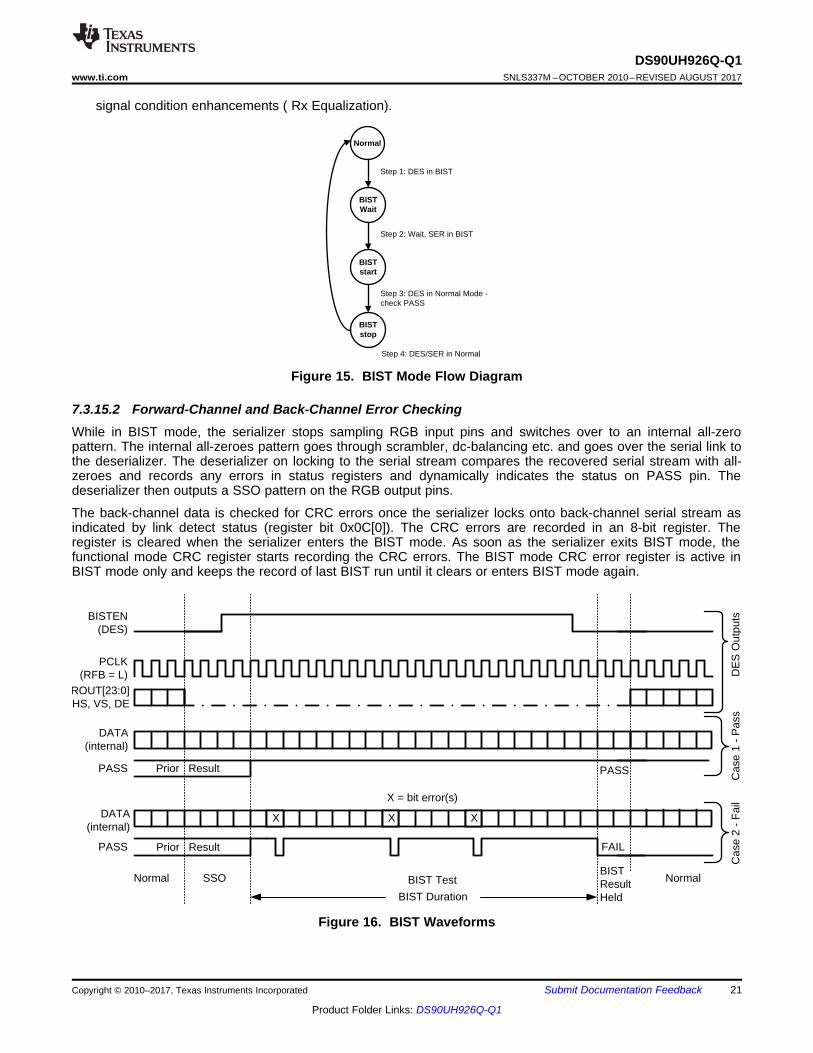
7.3.15 Built In Self Test (BIST)An optional At-Speed, Built-In Self Test (BIST) feature supports the testing of the high speed serial link and thelow- speed back channel. This is useful in the prototype stage, equipment production, in-system test and also forsystem diagnostics. The BIST is not available in backwards-compatible mode.
7.3.15.1 BIST Configuration and StatusThe BIST mode is enabled at the deserializer by the Pin select (Pin 44 BISTEN and Pin 16 BISTC) orconfiguration register (Table 11) through the deserializer. When LFMODE = 0, the pin based configurationdefaults to external PCLK or 33 MHz internal Oscillator clock (OSC) frequency. In the absence of PCLK, the usercan select the desired OSC frequency (default 33 MHz or 25 MHz) through the register bit. When LFMODE = 1,the pin based configuration defaults to external PCLK or 12.5 MHz MHz internal Oscillator clock (OSC)frequency.
When BISTEN of the deserializer is high, the BIST mode enable information is sent to the serializer through theBack Channel. The serializer outputs a test pattern and drives the link at speed. The deserializer detects the testpattern and monitors it for errors. The PASS output pin toggles to flag any payloads that are received with 1- to35-bit errors.
The BIST status is monitored real time on PASS pin. The result of the test is held on the PASS output until reset(new BIST test or Power Down). A High on PASS indicates NO ERRORS were detected. A Low on PASSindicates one or more errors were detected. The duration of the test is controlled by the pulse width applied tothe deserializer BISTEN pin. This BIST feature also contains a Link Error Count and a Lock Status. If theconnection of the serial link is broken, then the link error count is shown in the register. When the PLL of thedeserializer is locked or unlocked, the lock status can be read in the register. See Table 11.
7.3.15.1.1 Sample BIST Sequence
See Figure 15 for the BIST mode flow diagram.1. For the DS90UH925Q-Q1 and DS90UH926Q-Q1 FPD-Link III chipset, BIST Mode is enabled through the
BISTEN pin of DS90UH926Q-Q1 FPD-Link III deserializer. The desired clock source is selected throughBISTC pin.
2. The DS90UH925Q-Q1 serializer is woken up through the back channel if it is not already on. The all zeropattern on the data pins is sent through the FPD-Link III to the deserializer. Once the serializer and thedeserializer are in BIST mode and the deserializer acquires Lock, the PASS pin of the deserializer goes highand BIST starts checking the data stream. If an error in the payload (1 to 35) is detected, the PASS pin willswitch low for one half of the clock period. During the BIST test, the PASS output can be monitored andcounted to determine the payload error rate.
3. To Stop the BIST mode, the deserializer BISTEN pin is set Low. The deserializer stops checking the data.The final test result is held on the PASS pin. If the test ran error free, the PASS output will be High. If therewas one or more errors detected, the PASS output will be Low. The PASS output state is held until a newBIST is run, the device is RESET, or Powered Down. The BIST duration is user controlled by the duration ofthe BISTEN signal.
4. The Link returns to normal operation after the deserializer BISTEN pin is low. Figure 16 shows the waveformdiagram of a typical BIST test for two cases. Case 1 is error free, and Case 2 shows one with multiple errors.In most cases it is difficult to generate errors due to the robustness of the link (differential data transmissionetc.), thus they may be introduced by greatly extending the cable length, faulting the interconnect, reducing
7.3.15.2 Forward-Channel and Back-Channel Error CheckingWhile in BIST mode, the serializer stops sampling RGB input pins and switches over to an internal all-zeropattern. The internal all-zeroes pattern goes through scrambler, dc-balancing etc. and goes over the serial link tothe deserializer. The deserializer on locking to the serial stream compares the recovered serial stream with all-zeroes and records any errors in status registers and dynamically indicates the status on PASS pin. Thedeserializer then outputs a SSO pattern on the RGB output pins.
The back-channel data is checked for CRC errors once the serializer locks onto back-channel serial stream asindicated by link detect status (register bit 0x0C[0]). The CRC errors are recorded in an 8-bit register. Theregister is cleared when the serializer enters the BIST mode. As soon as the serializer exits BIST mode, thefunctional mode CRC register starts recording the CRC errors. The BIST mode CRC error register is active inBIST mode only and keeps the record of last BIST run until it clears or enters BIST mode again.
7.3.16 Image Enhancement FeaturesSeveral image enhancement features are provided. White balance LUTs allow the user to define and target thecolor temperature of the display. Adaptive Hi-FRC dithering enables the presentation of “true-color” images on an18–bit color display.
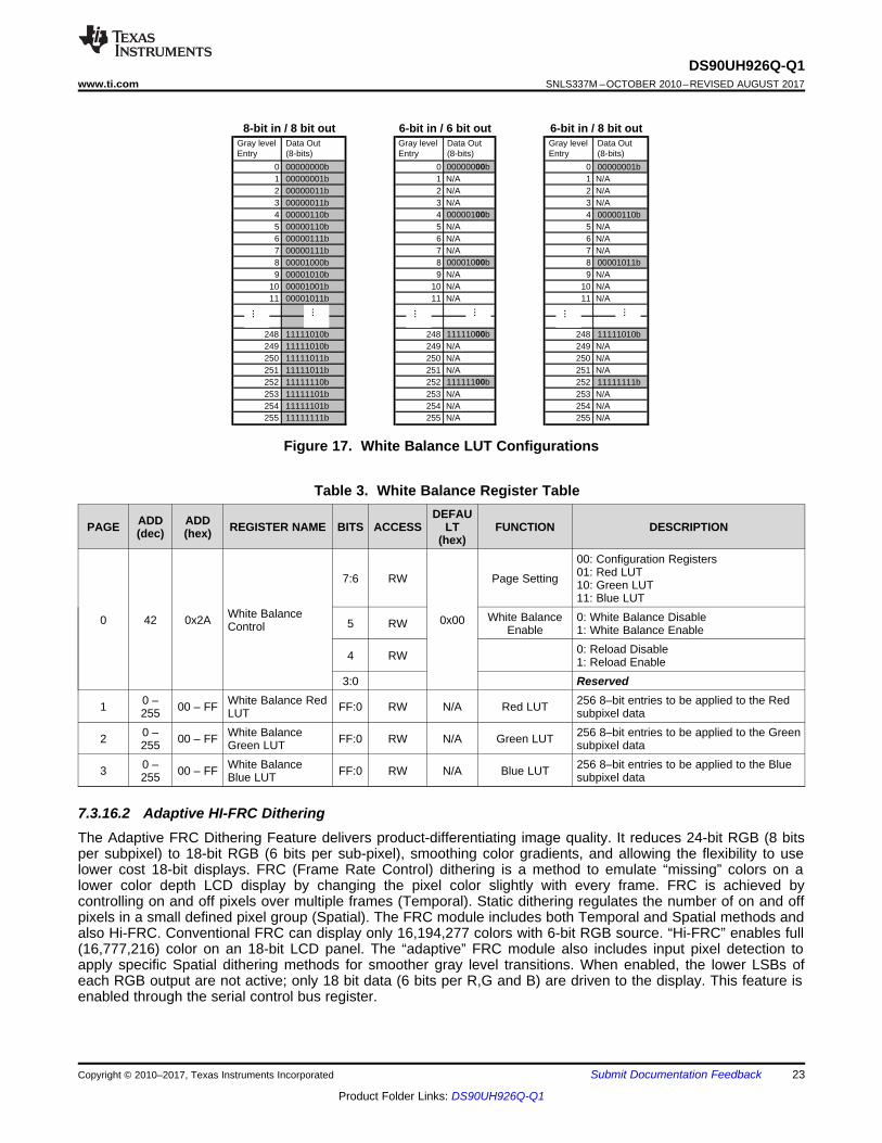
7.3.16.1 White BalanceThe White Balance feature enables similar display appearance when using LCDs from different vendors. Itcompensates for native color temperature of the display, and adjusts relative intensities of R, G, B to maintainspecified color temperature. Programmable control registers are used to define the contents of three LUTs (8-bitcolor value for Red, Green and Blue) for the white balance feature. The LUTs map input RGB values to newoutput RGB values. There are three LUTs, one LUT for each color. Each LUT contains 256 entries, 8 bits perentry with a total size of 6144 bits (3 x 256 x 8). All entries are readable and writable. Calibrated values areloaded into registers through the I2C interface (deserializer is a slave device). This feature may also be appliedto lower color depth applications such as 18–bit (666) and 16–bit (565). White balance is enabled and configuredthrough that serial control bus register.
7.3.16.1.1 LUT Contents
The user must define and load the contents of the LUT for each color (R,G,B). Regardless of the color depthbeing driven (888, 666, 656), the user must always provide contents for 3 complete LUTs - 256 colors x 8 bits x 3tables. Unused bits - LSBs -shall be set to 0 by the user.
When 24-bit (888) input data is being driven to a 24-bit display, each LUT (R, G and B) must contain 256 unique8-bit entries. The 8-bit white balanced data is then available at the output of the DS90UH926Q-Q1 deserializer,and driven to the display.
When 18-bit (666) input data is being driven to an 18-bit display, the white balance feature may be used in one oftwo ways. First, simply load each LUT with 256, 8-bit entries. Each 8-bit entry is a 6-bit value (6 MSBs) with the 2LSBs set to 00. Thus as total of 64 unique 6-bit white balance output values are available for each color (R, Gand B). The 6-bit white balanced data is available at the output of the DS90UH926Q-Q1 deserializer, and drivendirectly to the display.
Alternatively, with 6-bit input data the user may choose to load complete 8-bit values into each LUT. This modeof operation provides the user with finer resolution at the LUT output to more closely achieve the desired whitepoint of the calibrated display. Although 8-bit data is loaded, only 64 unique 8-bit white balance output values areavailable for each color (R, G and B). The result is 8-bit white balanced data. Before driving to the output of thedeserializer, the 8-bit data must be reduced to 6-bit with an FRC dithering function. To operate in this mode, theuser must configure the DS90UH926Q-Q1 to enable the FRC2 function.
Examples of the three types of LUT configurations described are shown in Figure 17
7.3.16.1.2 Enabling White Balance
The user must load all 3 LUTs prior to enabling the white balance feature. The following sequence must befollowed by the user.
To initialize white balance after power-on (Table 3):1. Load contents of all 3 LUTs . This requires a sequential loading of LUTs - first RED, second GREEN, third
BLUE. 256, 8-bit entries must be loaded to each LUT. Page registers must be set to select each LUT.2. Enable white balance.
By default, the LUT data may not be reloaded after initialization at power-on.
An option does exist to allow LUT reloading after power-on and initial LUT loading (as described above). Thisoption may only be used after enabling the white balance reload feature through the associated serial control busregister. In this mode the LUTs may be reloaded by the master controller through the I2C. This provides the userwith the flexibility to refresh LUTs periodically , or upon system requirements to change to a new set of LUTvalues. The host controller loads the updated LUT values through the serial bus interface. There is no need todisable the white balance feature while reloading the LUT data. Refreshing the white balance to the new set ofLUT data will be seamless - no interruption of displayed data.
It is important to note that initial loading of LUT values requires that all three LUTs be loaded sequentially. Whenreloading, partial LUT updates may be made.
00: Configuration Registers01: Red LUT10: Green LUT11: Blue LUT
5 RW White BalanceEnable
0: White Balance Disable1: White Balance Enable
4 RW 0: Reload Disable1: Reload Enable
3:0 Reserved
1 0 –255 00 – FF White Balance Red
LUT FF:0 RW N/A Red LUT 256 8–bit entries to be applied to the Redsubpixel data
2 0 –255 00 – FF White Balance
Green LUT FF:0 RW N/A Green LUT 256 8–bit entries to be applied to the Greensubpixel data
3 0 –255 00 – FF White Balance
Blue LUT FF:0 RW N/A Blue LUT 256 8–bit entries to be applied to the Bluesubpixel data
7.3.16.2 Adaptive HI-FRC DitheringThe Adaptive FRC Dithering Feature delivers product-differentiating image quality. It reduces 24-bit RGB (8 bitsper subpixel) to 18-bit RGB (6 bits per sub-pixel), smoothing color gradients, and allowing the flexibility to uselower cost 18-bit displays. FRC (Frame Rate Control) dithering is a method to emulate “missing” colors on alower color depth LCD display by changing the pixel color slightly with every frame. FRC is achieved bycontrolling on and off pixels over multiple frames (Temporal). Static dithering regulates the number of on and offpixels in a small defined pixel group (Spatial). The FRC module includes both Temporal and Spatial methods andalso Hi-FRC. Conventional FRC can display only 16,194,277 colors with 6-bit RGB source. “Hi-FRC” enables full(16,777,216) color on an 18-bit LCD panel. The “adaptive” FRC module also includes input pixel detection toapply specific Spatial dithering methods for smoother gray level transitions. When enabled, the lower LSBs ofeach RGB output are not active; only 18 bit data (6 bits per R,G and B) are driven to the display. This feature isenabled through the serial control bus register.
Two FRC functional blocks are available, and may be independently enabled. FRC1 precedes the white balanceLUT, and is intended to be used when 24-bit data is being driven to an 18-bit display with a white balance LUTthat is calibrated for an 18-bit data source. The second FRC block, FRC2, follows the white balance block and isintended to be used when fine adjustment of color temperature is required on an 18-bit color display, or when a24-bit source drives an 18-bit display with a white balance LUT calibrated for 24-bit source data.
For proper operation of the FRC dithering feature, the user must provide a description of the display timingcontrol signals. The timing mode, “sync mode” (HS, VS) or “DE only” must be specified, along with the activepolarity of the timing control signals. All this information is entered to DS90UH926Q-Q1 control registers throughthe serial bus interface.
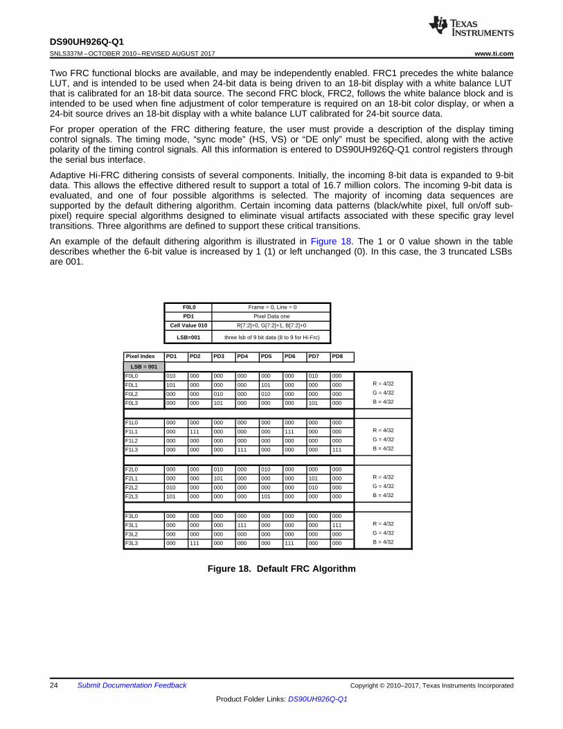
Adaptive Hi-FRC dithering consists of several components. Initially, the incoming 8-bit data is expanded to 9-bitdata. This allows the effective dithered result to support a total of 16.7 million colors. The incoming 9-bit data isevaluated, and one of four possible algorithms is selected. The majority of incoming data sequences aresupported by the default dithering algorithm. Certain incoming data patterns (black/white pixel, full on/off sub-pixel) require special algorithms designed to eliminate visual artifacts associated with these specific gray leveltransitions. Three algorithms are defined to support these critical transitions.
An example of the default dithering algorithm is illustrated in Figure 18. The 1 or 0 value shown in the tabledescribes whether the 6-bit value is increased by 1 (1) or left unchanged (0). In this case, the 3 truncated LSBsare 001.
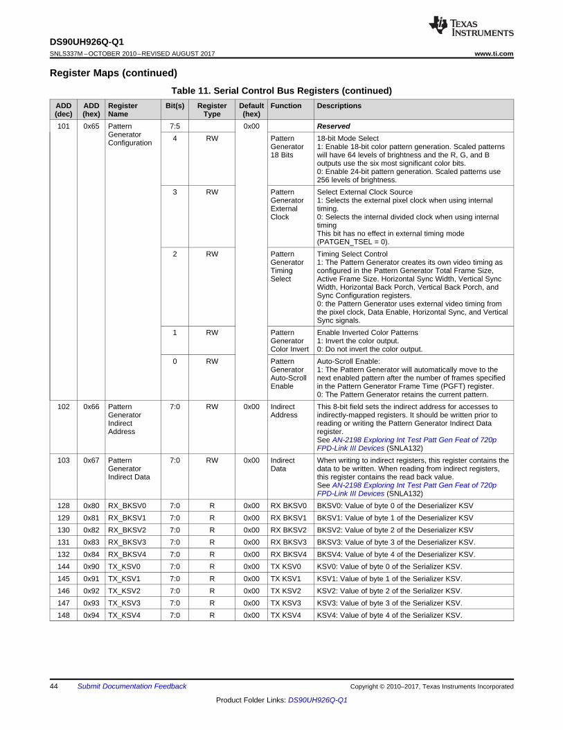
7.3.17 Internal Pattern GenerationThe DS90UH926Q-Q1 serializer supports the internal pattern generation feature. It allows basic testing anddebugging of an integrated panel. The test patterns are simple and repetitive and allow for a quick visualverification of panel operation. As long as the device is not in power down mode, the test pattern will bedisplayed even if no parallel input is applied. If no PCLK is received, the test pattern can be configured to use aprogrammed oscillator frequency. For detailed information, refer to AN-2198 Exploring the Internal Test PatternGeneration Feature of 720p FPD-Link III Devices (SNLA132).
7.3.18 I2S ReceivingIn normal 24-bit RGB operation mode, the DS90UH926Q-Q1 provides up to 3-bit of I2S. They are I2S_CLK,I2S_WC and I2S_DA, as well as the Master I2S Clock (MCLK). The audio is received through the forward videoframe, or can be configured to receive during video blanking periods. A jitter cleaning feature reduces I2S_CLKoutput jitter to +/- 2ns. The encrypted and packetized audio information is received during the video blankingperiods along with specific information about the clock frequency. The bit rates of any I2S input bits mustmaintain one fourth of the PCLK rate. The audio decryption is supported per HDCP v1.3.
7.3.18.1 I2S Jitter CleaningIn 18-bit RGB operation mode, the secondary I2S data (I2S_DB) can be used as the additional I2S audiochannel in additional to the 3–bit of I2S. The I2S_DB is synchronized to the I2S_CLK. To enable thissynchronization feature on this bit, set the MODE_SEL (Table 9) or program through the register bit ()
7.3.18.2 Secondary I2S ChannelIn 18-bit RGB operation mode, the secondary I2S data (I2S_DB) can be used as the additional I2S audiochannel in additional to the 3–bit of I2S. The I2S_DB is synchronized to the I2S_CLK. To enable thissynchronization feature on this bit, set the MODE_SEL (Table 9) or program through the register bit (Table 11).
7.3.18.2.1 MCLK
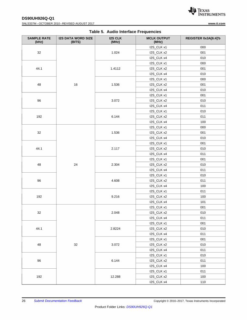
The deserializer has an I2S Master Clock Output. It supports x1, x2, or x4 of I2S CLK Frequency. When the I2SPLL is disabled, the MCLK output is off. Table 5 below covers the range of I2S sample rates and MCLKfrequencies. By default, all the MCLK output frequencies are x2 of the I2S CLK frequencies. The MCLKfrequencies can also be enabled through the register bit [7:4] (I2S MCLK Output) of 0x3A shown in Table 11. Toselect desired MCLK frequency, write bit 7 (0x3A) = 1, then write to bit [6:4] accordingly.
7.3.19 Interrupt Pin: Functional Description and Usage (INTB)1. On DS90UH925Q-Q1, set register 0xC6[5] = 1 and 0xC6[0] = 12. DS90UH926Q-Q1 deserializer INTB_IN (pin 16) is set LOW by some downstream device.3. DS90UH925Q-Q1 serializer pulls INTB (pin 31) LOW. The signal is active low, so a LOW indicates an
interrupt condition.4. External controller detects INTB = LOW; to determine interrupt source, read HDCP_ISR register .5. A read to HDCP_ISR will clear the interrupt at the DS90UH925, releasing INTB.6. The external controller typically must then access the remote device to determine downstream interrupt
source and clear the interrupt driving INTB_IN. This would be when the downstream device releases theINTB_IN (pin 16) on the DS90UH926Q-Q1. The system is now ready to return to step (1) at next falling edgeof INTB_IN.
7.3.20 GPIO[3:0] and GPO_REG[8:4]In 18-bit RGB operation mode, the optional R[1:0] and G[1:0] of the DS90UH926Q-Q1 can be used as thegeneral purpose IOs GPIO[3:0] in either forward channel (Outputs) or back channel (Inputs) application.
7.3.20.1 GPIO[3:0] Enable SequenceSee Table 6 for the GPIO enable sequencing.1. Enable the 18-bit mode either through the configuration register bit Table 11 on DS90UH925Q-Q1 only.
DS90UH926Q-Q1 is automatically configured as in the 18-bit mode.2. To enable GPIO3 forward channel, write 0x03 to address 0x0F on DS90UH925Q-Q1, then write 0x05 to
7.3.20.2 GPO_REG[8:4] Enable SequenceGPO_REG[8:4] are the outputs only pins. They must be programmed through the local register bits. SeeTable 11 for the GPO_REG enable sequencing.1. Enable the 18-bit mode either through the configuration register bit Table 11 on DS90UH925Q-Q1 only.
DS90UH926Q-Q1 is automatically configured as in the 18-bit mode.2. To enable GPO_REG8 outputs a 1, write 0x90 to address 0x11 on DS90UH925Q.
Table 7. GPO_REG Enable Sequencing TableNO. DESCRIPTION DEVICE LOCAL ACCESS LOCAL OUTPUT VALUE
7.4.1 Clock-Data Recovery Status Flag (LOCK), Output Enable (OEN), and Output State Select(OSS_SEL)
When PDB is driven HIGH, the CDR PLL begins locking to the serial input and LOCK is TRI-STATE or LOW(depending on the value of the OEN setting). After the DS90UH926Q-Q1 completes its lock sequence to theinput serial data, the LOCK output is driven HIGH, indicating valid data and clock recovered from the serial inputis available on the parallel bus and PCLK outputs. The State of the outputs are based on the OEN andOSS_SEL setting (Table 8) or register bit (Table 11). See Figure 7.
X 0 X X Z Z Z ZX 1 0 0 L or H L L LX 1 0 1 L or H Z Z Z
Static 1 1 0 L L L L/OSC (Register bitenable)
Static 1 1 1 L Previous Status L LActive 1 1 0 H L L LActive 1 1 1 H Valid Valid Valid
7.4.2 Low Frequency Optimization (LFMODE)The LFMODE is set through a register (Table 11) or MODE_SEL Pin 24 (Table 9). It controls the operatingfrequency of the deserializer. If LFMODE is Low (default), the PCLK frequency is between 15 MHz and 85 MHz.If LFMODE is High, the PCLK frequency is between 5 MHz and <15 MHz. Please note: when the deviceLFMODE is changed, a PDB reset is required.
7.4.3 Configuration Select (MODE_SEL)Configuration of the device may be done through the MODE_SEL input pin, or through the configuration registerbit. A pullup resistor and a pulldown resistor of suggested values may be used to set the voltage ratio of theMODE_SEL input (VR4) and VDD33 to select one of the other 10 possible selected modes. See Figure 19 andTable 9.
(1) LFMODE:L = frequency range is 15 MHz to 85 MHz (Default)H = frequency range is 5 to < 15 MHz
(2) Repeater:L = Repeater mode is OFF (Default)H = Repeater mode is ON
(3) Backward Compatible:L = Backward Compatible mode is OFF (Default)H = Backward Compatible mode is ON; SER = DS90UR905Q or DS90UR907Q
– frequency range = 15 to 65 MHz, set LFMODE = L(4) I2S Channel B:
L = I2S Channel B mode is OFF, normal 24-bit RGB Mode (Default)H = I2S Channel B mode is ON, 18-bit RGB Mode with I2S_DB Enabled. Note: use of GPIO(s) on unused inputs must be enabled by
register.
Table 9. Configuration Select (MODE_SEL)
NO.IDEALRATIO
VR4/VDD33
IDEAL VR4(V)
SUGGESTEDRESISTOR R3
kΩ (1% tol)
SUGGESTEDRESISTOR R4
kΩ (1% tol)LFMODE (1) REPEATER (2) BACKWARD
COMPATIBLE (3)I2S CHANNEL B(18–bit MODE) (4)
1 0 0 Open 40.2 L L L L2 0.123 0.407 115 16.2 L L L H3 0.167 0.552 121 24.3 L H L L4 0.227 0.748 162 47.5 L H L H5 0.291 0.960 137 56.2 H L L L6 0.366 1.209 107 61.9 H L L H7 0.458 1.510 113 95.3 H H L L8 0.542 1.790 95.3 113 H H L H9 0.611 2.016 73.2 115 L L H L
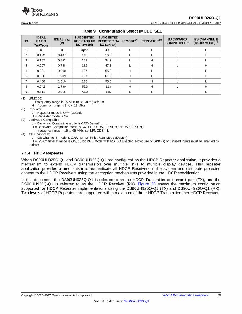
7.4.4 HDCP RepeaterWhen DS90UH925Q-Q1 and DS90UH926Q-Q1 are configured as the HDCP Repeater application, it provides amechanism to extend HDCP transmission over multiple links to multiple display devices. This repeaterapplication provides a mechanism to authenticate all HDCP Receivers in the system and distribute protectedcontent to the HDCP Receivers using the encryption mechanisms provided in the HDCP specification.
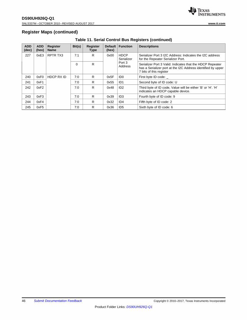
In this document, the DS90UH925Q-Q1 is referred to as the HDCP Transmitter or transmit port (TX), and theDS90UH926Q-Q1 is referred to as the HDCP Receiver (RX). Figure 20 shows the maximum configurationsupported for HDCP Repeater implementations using the DS90UH925Q-Q1 (TX) and DS90UH926Q-Q1 (RX).Two levels of HDCP Repeaters are supported with a maximum of three HDCP Transmitters per HDCP Receiver.
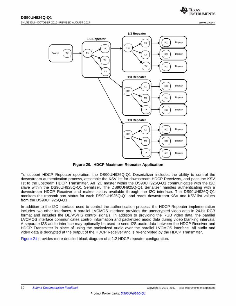
To support HDCP Repeater operation, the DS90UH926Q-Q1 Deserializer includes the ability to control thedownstream authentication process, assemble the KSV list for downstream HDCP Receivers, and pass the KSVlist to the upstream HDCP Transmitter. An I2C master within the DS90UH926Q-Q1 communicates with the I2Cslave within the DS90UH925Q-Q1 Serializer. The DS90UH925Q-Q1 Serializer handles authenticating with adownstream HDCP Receiver and makes status available through the I2C interface. The DS90UH926Q-Q1monitors the transmit port status for each DS90UH925Q-Q1 and reads downstream KSV and KSV list valuesfrom the DS90UH925Q-Q1.
In addition to the I2C interface used to control the authentication process, the HDCP Repeater implementationincludes two other interfaces. A parallel LVCMOS interface provides the unencrypted video data in 24-bit RGBformat and includes the DE/VS/HS control signals. In addition to providing the RGB video data, the parallelLVCMOS interface communicates control information and packetized audio data during video blanking intervals.A separate I2S audio interface may optionally be used to send I2S audio data between the HDCP Receiver andHDCP Transmitter in place of using the packetized audio over the parallel LVCMOS interface. All audio andvideo data is decrypted at the output of the HDCP Receiver and is re-encrypted by the HDCP Transmitter.
Figure 21 provides more detailed block diagram of a 1:2 HDCP repeater configuration.
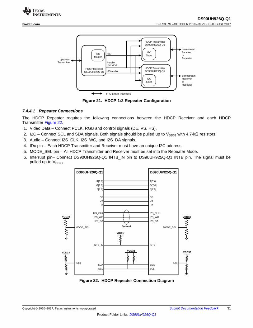
7.4.4.1 Repeater ConnectionsThe HDCP Repeater requires the following connections between the HDCP Receiver and each HDCPTransmitter Figure 22.1. Video Data – Connect PCLK, RGB and control signals (DE, VS, HS).2. I2C – Connect SCL and SDA signals. Both signals should be pulled up to VDD33 with 4.7-kΩ resistors3. Audio – Connect I2S_CLK, I2S_WC, and I2S_DA signals.4. IDx pin – Each HDCP Transmitter and Receiver must have an unique I2C address.5. MODE_SEL pin – All HDCP Transmitter and Receiver must be set into the Repeater Mode.6. Interrupt pin– Connect DS90UH926Q-Q1 INTB_IN pin to DS90UH925Q-Q1 INTB pin. The signal must be
7.5.1 Serial Control BusThe DS90UH926Q-Q1 is configured by the use of a serial control bus that is I2C protocol compatible. . Multipledeserializer devices may share the serial control bus since 16 device addresses are supported. Device addressis set through the R1 and R2 values on IDx pin. See Figure 23.
The serial control bus consists of two signals and a configuration pin. The SCL is a Serial Bus Clock Input /Output. The SDA is the Serial Bus Data Input / Output signal. Both SCL and SDA signals require an externalpull-up resistor to VDD33. For most applications a 4.7 kΩ pull-up resistor to VDD33 may be used. The resistor valuemay be adjusted for capacitive loading and data rate requirements. The signals are either pulled High, or drivenLow.
Figure 23. Serial Control Bus Connection
The configuration pin is the IDx pin. This pin sets one of 16 possible device addresses. A pull-up resistor and apull-down resistor of suggested values may be used to set the voltage ratio of the IDx input (VR2) and VDD33 toselect one of the other 16 possible addresses. See Table 10
Backward Compatible (BC) mode set by MODE_SEL pinor register.1: BC is set by register bit. Use register bit reg_0x02[2] toset BC Mode0: Use MODE_SEL pin.
2 RW BackwardCompatibleModeSelect
Backward compatible (BC) mode to DS90UR905Q orDS90UR907Q, if reg_0x02[3] = 11: Backward compatible with DS90UR905Q orDS90UR907Q(Set LFMODE = 0)0: Backward Compatible is OFF (default)
1 RW LFMODEselect bypin orregistercontrol
Frequency range is set by MODE_SEL pin or register1: Frequency range is set by register. Use registerbitreg_0x02[0] to set LFMODE0: Frequency range is set by MODE_SEL pin.
0 RW LFMODE Frequency range select1: PCLK range = 5 to <15 MHz, if reg_0x02[1] = 10: PCLK range = 15 to 85 MHz (default)
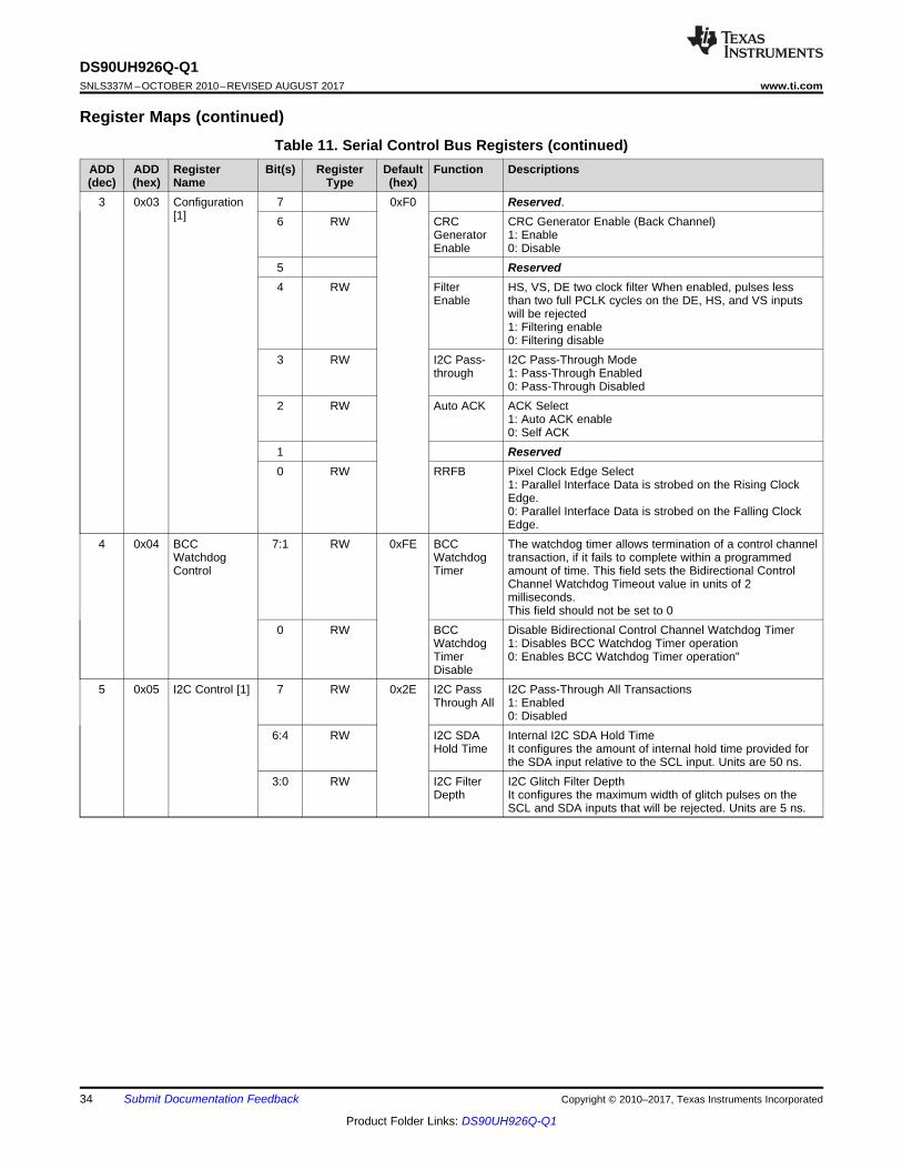
EnableHS, VS, DE two clock filter When enabled, pulses lessthan two full PCLK cycles on the DE, HS, and VS inputswill be rejected1: Filtering enable0: Filtering disable
2 RW Auto ACK ACK Select1: Auto ACK enable0: Self ACK
1 Reserved0 RW RRFB Pixel Clock Edge Select
1: Parallel Interface Data is strobed on the Rising ClockEdge.0: Parallel Interface Data is strobed on the Falling ClockEdge.
4 0x04 BCCWatchdogControl
7:1 RW 0xFE BCCWatchdogTimer
The watchdog timer allows termination of a control channeltransaction, if it fails to complete within a programmedamount of time. This field sets the Bidirectional ControlChannel Watchdog Timeout value in units of 2milliseconds.This field should not be set to 0
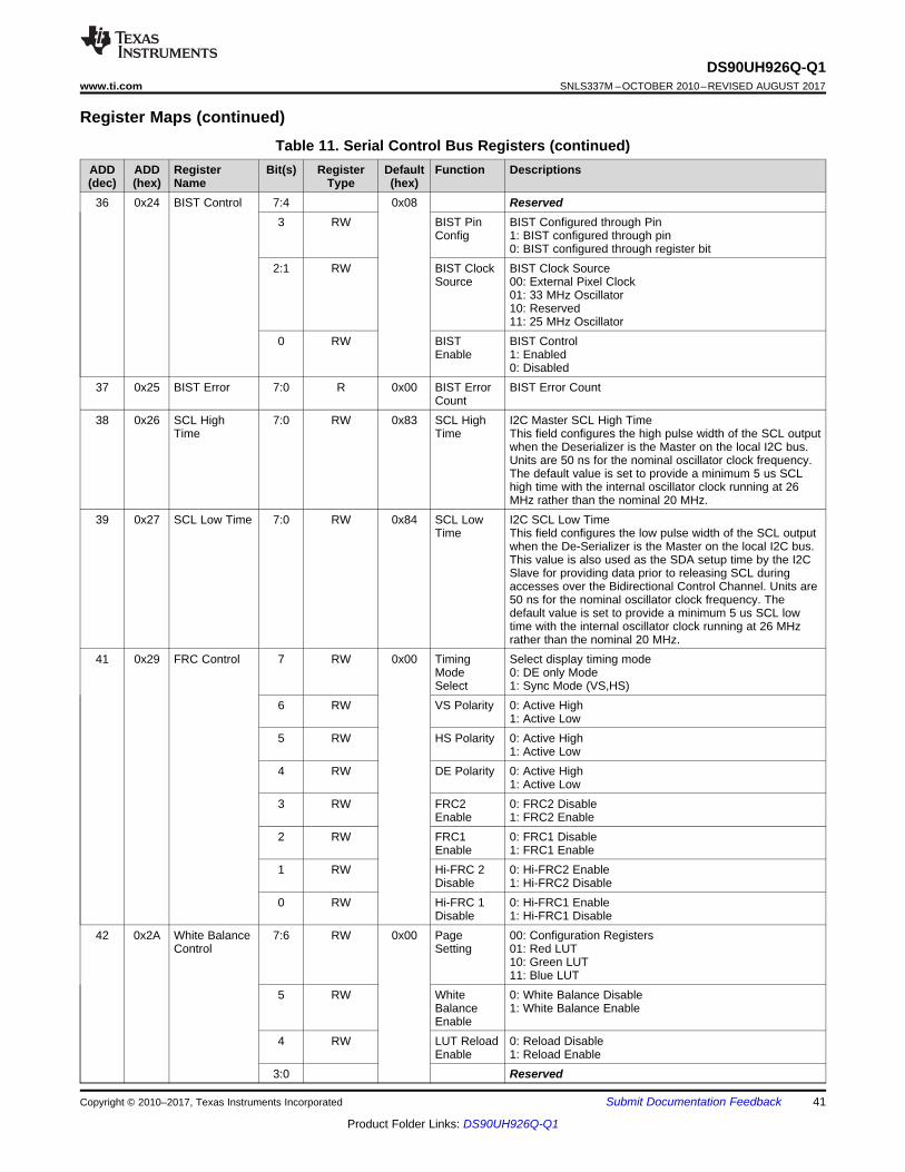
Register Maps (continued)Table 11. Serial Control Bus Registers (continued)
ADD(dec)
ADD(hex)
RegisterName
Bit(s) RegisterType
Default(hex)
Function Descriptions
6 0x06 I2C Control [2] 7 R 0x00 ForwardChannelSequenceError
Control Channel Sequence Error Detected It indicates asequence error has been detected in forward controlchannel. It this bit is set, an error may have occurred in thecontrol channel operation.
6 RW ClearSequenceError
It clears the Sequence Error Detect bitThis bit is not self-clearing.
5 Reserved4:3 RW SDA Output
DelaySDA Output DelayThis field configures output delay on the SDA output.Setting this value will increase output delay in units of 50ns. Nominal output delay values for SCL to SDA are:00 : 250 ns01: 300 ns10: 350 ns11: 400 ns
2 RW Local Write Disable Remote Writes to Local Registers throughSerializer (Does not affect remote access to I2C slaves atDeserializer)1: Stop remote write to local device registers0: remote write to local device registers
1 RW I2C BusTimerSpeed
Speed up I2C Bus Watchdog Timer1: Timer expires after approximately 50 ms0: Timer expires after approximately 1 s
0 RW I2C BusTimerDisable
Disable I2C Bus Timer When the I2C Timer may be usedto detect when the I2C bus is free or hung up following aninvalid termination of a transaction. If SDA is high and nosignalling occurs for approximately 1 s, the I2C bus isassumed to be free. If SDA is low and no signaling occurs,the device will try to clear the bus by driving 9 clocks onSCL
7 0x07 RemoteDevice ID
7:1 RW 0x18 Remote ID Remote IDConfigures the I2C Slave ID of the remote Serializer. Avalue of 0 in this field disables I2C access to remoteSerializer. This field is automatically configured through theSerializer Forward Channel. Software may overwrite thisvalue, but should also set the FREEZE DEVICE ID bit toprevent overwriting by the Forward Channel.
0 RW FreezeDevice ID
Freeze Serializer Device ID1: Prevent auto-loading of the Serializer Device ID from theForward Channel. The ID will be frozen at the valuewritten.0: Update
7-bit Remote Slave Device ID 0Configures the physical I2C address of the remote I2CSlave device attached to the remote Serializer. If an I2Ctransaction is addressed to the Slave Alias ID0, thetransaction will be remapped to this address beforepassing the transaction across the Bidirectional ControlChannel to the Serializer.
0 Reserved9 0x09 SlaveID[1] 7:1 RW 0x00 Target
SlaveDevice ID1
7-bit Remote Slave Device ID 1Configures the physical I2C address of the remote I2CSlave device attached to the remote Serializer. If an I2Ctransaction is addressed to the Slave Alias ID1, thetransaction will be remapped to this address beforepassing the transaction across the Bidirectional ControlChannel to the Serializer.
7-bit Remote Slave Device ID 2Configures the physical I2C address of the remote I2CSlave device attached to the remote Serializer. If an I2Ctransaction is addressed to the Slave Alias ID2, thetransaction will be remapped to this address beforepassing the transaction across the Bidirectional ControlChannel to the Serializer.
0 Reserved11 0x0B SlaveID[3] 7:1 RW 0x00 Target
SlaveDevice ID3
7-bit Remote Slave Device ID 3Configures the physical I2C address of the remote I2CSlave device attached to the remote Serializer. If an I2Ctransaction is addressed to the Slave Alias ID3, thetransaction will be remapped to this address beforepassing the transaction across the Bidirectional ControlChannel to the Serializer.
0 Reserved12 0x0C SlaveID[4] 7:1 RW 0x00 Target
SlaveDevice ID4
7-bit Remote Slave Device ID 4Configures the physical I2C address of the remote I2CSlave device attached to the remote Serializer. If an I2Ctransaction is addressed to the Slave Alias ID4, thetransaction will be remapped to this address beforepassing the transaction across the Bidirectional ControlChannel to the Serializer.
0 Reserved13 0x0D SlaveID[5] 7:1 RW 0x00 Target
SlaveDevice ID5
7-bit Remote Slave Device ID 5Configures the physical I2C address of the remote I2CSlave device attached to the remote Serializer. If an I2Ctransaction is addressed to the Slave Alias ID5, thetransaction will be remapped to this address beforepassing the transaction across the Bidirectional ControlChannel to the Serializer.
0 Reserved14 0x0E SlaveID[6] 7:1 RW 0x00 Target
SlaveDevice ID6
7-bit Remote Slave Device ID 6Configures the physical I2C address of the remote I2CSlave device attached to the remote Serializer. If an I2Ctransaction is addressed to the Slave Alias ID6, thetransaction will be remapped to this address beforepassing the transaction across the Bidirectional ControlChannel to the Serializer.
0 Reserved15 0x0F SlaveID[7] 7:1 RW 0x00 Target
SlaveDevice ID7
7-bit Remote Slave Device ID 7Configures the physical I2C address of the remote I2CSlave device attached to the remote Serializer. If an I2Ctransaction is addressed to the Slave Alias ID7, thetransaction will be remapped to this address beforepassing the transaction across the Bidirectional ControlChannel to the Serializer.
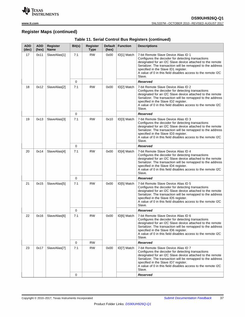
0 Reserved16 0x10 SlaveAlias[0] 7:1 RW 0x00 ID[0] Match 7-bit Remote Slave Device Alias ID 0
Configures the decoder for detecting transactionsdesignated for an I2C Slave device attached to the remoteSerializer. The transaction will be remapped to the addressspecified in the Slave ID0 register.A value of 0 in this field disables access to the remote I2CSlave.
Register Maps (continued)Table 11. Serial Control Bus Registers (continued)
ADD(dec)
ADD(hex)
RegisterName
Bit(s) RegisterType
Default(hex)
Function Descriptions
17 0x11 SlaveAlias[1] 7:1 RW 0x00 ID[1] Match 7-bit Remote Slave Device Alias ID 1Configures the decoder for detecting transactionsdesignated for an I2C Slave device attached to the remoteSerializer. The transaction will be remapped to the addressspecified in the Slave ID1 register.A value of 0 in this field disables access to the remote I2CSlave.
0 Reserved18 0x12 SlaveAlias[2] 7:1 RW 0x00 ID[2] Match 7-bit Remote Slave Device Alias ID 2
Configures the decoder for detecting transactionsdesignated for an I2C Slave device attached to the remoteSerializer. The transaction will be remapped to the addressspecified in the Slave ID2 register.A value of 0 in this field disables access to the remote I2CSlave.
0 Reserved19 0x13 SlaveAlias[3] 7:1 RW 0x10 ID[3] Match 7-bit Remote Slave Device Alias ID 3
Configures the decoder for detecting transactionsdesignated for an I2C Slave device attached to the remoteSerializer. The transaction will be remapped to the addressspecified in the Slave ID3 register.A value of 0 in this field disables access to the remote I2CSlave.
0 Reserved20 0x14 SlaveAlias[4] 7:1 RW 0x00 ID[4] Match 7-bit Remote Slave Device Alias ID 4
Configures the decoder for detecting transactionsdesignated for an I2C Slave device attached to the remoteSerializer. The transaction will be remapped to the addressspecified in the Slave ID4 register.A value of 0 in this field disables access to the remote I2CSlave.
0 Reserved21 0x15 SlaveAlias[5] 7:1 RW 0x00 ID[5] Match 7-bit Remote Slave Device Alias ID 5
Configures the decoder for detecting transactionsdesignated for an I2C Slave device attached to the remoteSerializer. The transaction will be remapped to the addressspecified in the Slave ID5 register.A value of 0 in this field disables access to the remote I2CSlave.
0 Reserved22 0x16 SlaveAlias[6] 7:1 RW 0x00 ID[6] Match 7-bit Remote Slave Device Alias ID 6
Configures the decoder for detecting transactionsdesignated for an I2C Slave device attached to the remoteSerializer. The transaction will be remapped to the addressspecified in the Slave ID6 register.A value of 0 in this field disables access to the remote I2CSlave.
0 RW Reserved23 0x17 SlaveAlias[7] 7:1 RW 0x00 ID[7] Match 7-bit Remote Slave Device Alias ID 7
Configures the decoder for detecting transactionsdesignated for an I2C Slave device attached to the remoteSerializer. The transaction will be remapped to the addressspecified in the Slave ID7 register.A value of 0 in this field disables access to the remote I2CSlave.
Register Maps (continued)Table 11. Serial Control Bus Registers (continued)
ADD(dec)
ADD(hex)
RegisterName
Bit(s) RegisterType
Default(hex)
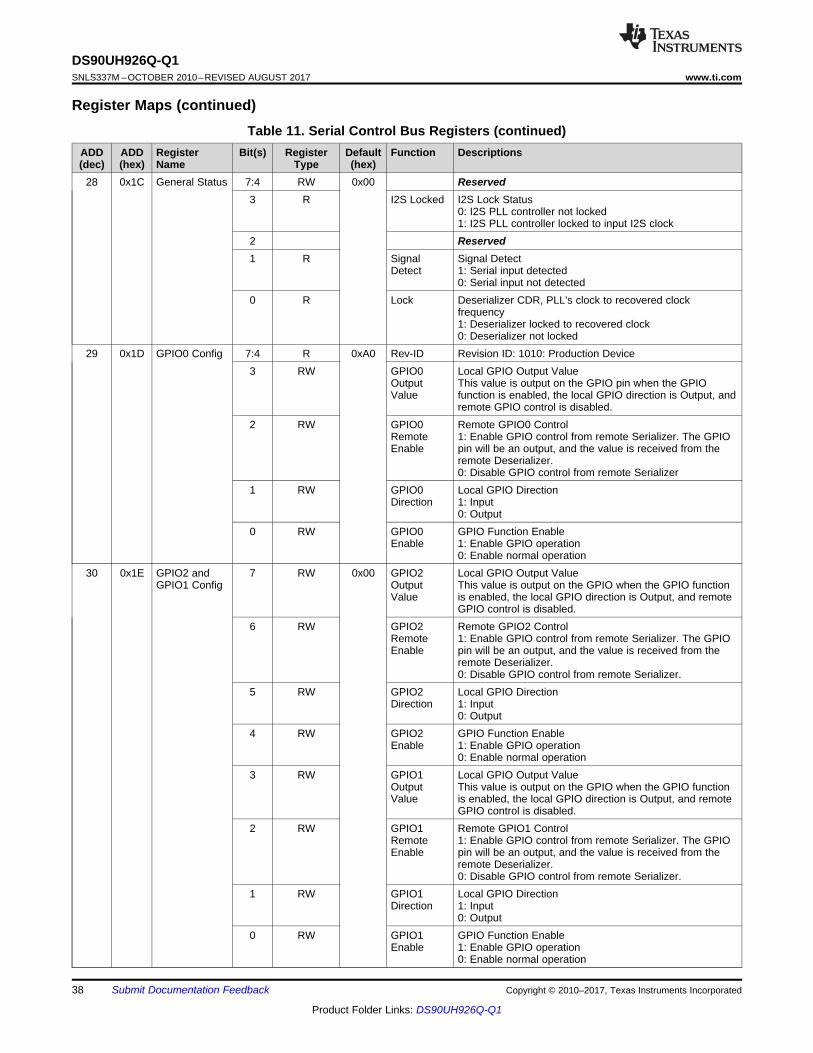
Function Descriptions
28 0x1C General Status 7:4 RW 0x00 Reserved3 R I2S Locked I2S Lock Status
0: I2S PLL controller not locked1: I2S PLL controller locked to input I2S clock
2 Reserved1 R Signal
DetectSignal Detect1: Serial input detected0: Serial input not detected
0 R Lock Deserializer CDR, PLL's clock to recovered clockfrequency1: Deserializer locked to recovered clock0: Deserializer not locked
29 0x1D GPIO0 Config 7:4 R 0xA0 Rev-ID Revision ID: 1010: Production Device3 RW GPIO0
OutputValue
Local GPIO Output ValueThis value is output on the GPIO pin when the GPIOfunction is enabled, the local GPIO direction is Output, andremote GPIO control is disabled.
2 RW GPIO0RemoteEnable
Remote GPIO0 Control1: Enable GPIO control from remote Serializer. The GPIOpin will be an output, and the value is received from theremote Deserializer.0: Disable GPIO control from remote Serializer
1 RW GPIO0Direction
Local GPIO Direction1: Input0: Output
0 RW GPIO0Enable
GPIO Function Enable1: Enable GPIO operation0: Enable normal operation
30 0x1E GPIO2 andGPIO1 Config
7 RW 0x00 GPIO2OutputValue
Local GPIO Output ValueThis value is output on the GPIO when the GPIO functionis enabled, the local GPIO direction is Output, and remoteGPIO control is disabled.
6 RW GPIO2RemoteEnable
Remote GPIO2 Control1: Enable GPIO control from remote Serializer. The GPIOpin will be an output, and the value is received from theremote Deserializer.0: Disable GPIO control from remote Serializer.
5 RW GPIO2Direction
Local GPIO Direction1: Input0: Output
4 RW GPIO2Enable
GPIO Function Enable1: Enable GPIO operation0: Enable normal operation
3 RW GPIO1OutputValue
Local GPIO Output ValueThis value is output on the GPIO when the GPIO functionis enabled, the local GPIO direction is Output, and remoteGPIO control is disabled.
2 RW GPIO1RemoteEnable
Remote GPIO1 Control1: Enable GPIO control from remote Serializer. The GPIOpin will be an output, and the value is received from theremote Deserializer.0: Disable GPIO control from remote Serializer.
1 RW GPIO1Direction
Local GPIO Direction1: Input0: Output
0 RW GPIO1Enable
GPIO Function Enable1: Enable GPIO operation0: Enable normal operation
Register Maps (continued)Table 11. Serial Control Bus Registers (continued)
ADD(dec)
ADD(hex)
RegisterName
Bit(s) RegisterType
Default(hex)
Function Descriptions
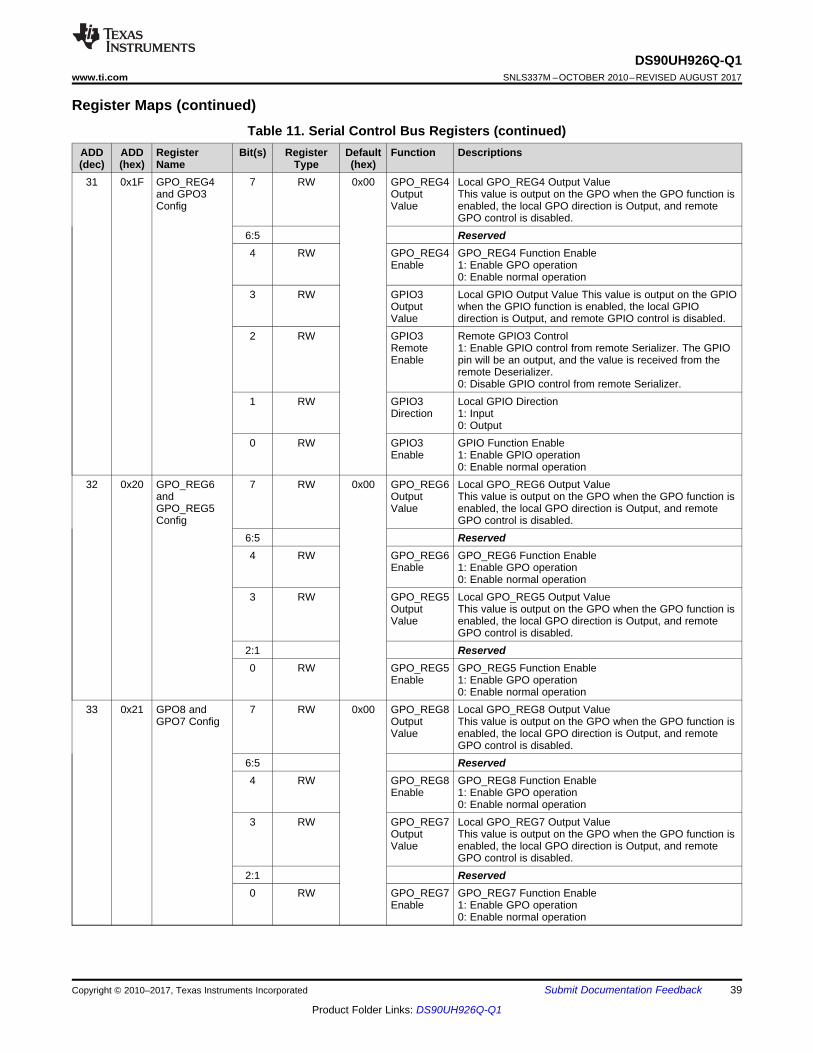
31 0x1F GPO_REG4and GPO3Config
7 RW 0x00 GPO_REG4OutputValue
Local GPO_REG4 Output ValueThis value is output on the GPO when the GPO function isenabled, the local GPO direction is Output, and remoteGPO control is disabled.
6:5 Reserved4 RW GPO_REG4
EnableGPO_REG4 Function Enable1: Enable GPO operation0: Enable normal operation
3 RW GPIO3OutputValue
Local GPIO Output Value This value is output on the GPIOwhen the GPIO function is enabled, the local GPIOdirection is Output, and remote GPIO control is disabled.
2 RW GPIO3RemoteEnable
Remote GPIO3 Control1: Enable GPIO control from remote Serializer. The GPIOpin will be an output, and the value is received from theremote Deserializer.0: Disable GPIO control from remote Serializer.
1 RW GPIO3Direction
Local GPIO Direction1: Input0: Output
0 RW GPIO3Enable
GPIO Function Enable1: Enable GPIO operation0: Enable normal operation
32 0x20 GPO_REG6andGPO_REG5Config
7 RW 0x00 GPO_REG6OutputValue
Local GPO_REG6 Output ValueThis value is output on the GPO when the GPO function isenabled, the local GPO direction is Output, and remoteGPO control is disabled.
6:5 Reserved4 RW GPO_REG6
EnableGPO_REG6 Function Enable1: Enable GPO operation0: Enable normal operation
3 RW GPO_REG5OutputValue
Local GPO_REG5 Output ValueThis value is output on the GPO when the GPO function isenabled, the local GPO direction is Output, and remoteGPO control is disabled.
2:1 Reserved0 RW GPO_REG5
EnableGPO_REG5 Function Enable1: Enable GPO operation0: Enable normal operation
33 0x21 GPO8 andGPO7 Config
7 RW 0x00 GPO_REG8OutputValue
Local GPO_REG8 Output ValueThis value is output on the GPO when the GPO function isenabled, the local GPO direction is Output, and remoteGPO control is disabled.
6:5 Reserved4 RW GPO_REG8
EnableGPO_REG8 Function Enable1: Enable GPO operation0: Enable normal operation
3 RW GPO_REG7OutputValue
Local GPO_REG7 Output ValueThis value is output on the GPO when the GPO function isenabled, the local GPO direction is Output, and remoteGPO control is disabled.
2:1 Reserved0 RW GPO_REG7
EnableGPO_REG7 Function Enable1: Enable GPO operation0: Enable normal operation
Register Maps (continued)Table 11. Serial Control Bus Registers (continued)
ADD(dec)
ADD(hex)
RegisterName
Bit(s) RegisterType
Default(hex)
Function Descriptions
34 0x22 Data PathControl
7 RW 0x00 Override FCConfig
1: Disable loading of this register from the forward channel,keeping locally written values intact0: Allow forward channel loading of this register
6 RW Pass RGB Setting this bit causes RGB data to be sent independent ofDE. This allows operation in systems which may not useDE to frame video data or send other data when DE isdeasserted. Note that setting this bit prevents HDCPoperation and blocks packetized audio. This bit does notneed to be set in DS90UB925 or in Backward Compatiblemode.1: Pass RGB independent of DE0: Normal operationNote: this bit is automatically loaded from the remoteserializer unless bit 7 of this register is set.
5 RW DE Polarity This bit indicates the polarity of the DE (Data Enable)signal.1: DE is inverted (active low, idle high)0: DE is positive (active high, idle low)Note: this bit is automatically loaded from the remoteserializer unless bit 7 of this register is set.
4 RW I2S_Gen This bit controls whether the HDCP Receiver outputspacketized Auxiliary/Audio data on the RGB video outputpins.1: Don't output packetized audio data on RGB video outputpins0: Output packetized audio on RGB video output pins.Note: this bit is automatically loaded from the remoteserializer unless bit 7 of this register is set.
3 RW I2S ChannelB EnableOverride
1: Set I2S Channel B Enable from reg_0x22[0]0: Set I2S Channel B Enable from MODE_SEL pinNote: this bit is automatically loaded from the remoteserializer unless bit 7 of this register is set.
2 RW 18-bit VideoSelect
1: Select 18-bit video modeNote: use of GPIO(s) on unused inputs must be enabledby register.0: Select 24-bit video modeNote: this bit is automatically loaded from the remoteserializer unless bit 7 of this register is set.
1 RW I2STransportSelect
1: Enable I2S Data Forward Channel Frame Transport0: Enable I2S Data Island TransportNote: this bit is automatically loaded from the remoteserializer unless bit 7 of this register is set.
0 RW I2S ChannelB Enable
I2S Channel B Enable1: Enable I2S Channel B on B1 output0: I2S Channel B disabledNote: this bit is automatically loaded from the remoteserializer unless bit 7 of this register is set.
35 0x23 GeneralPurposeControl
7 RW 0x10 Rx RGBChecksum
RX RGB Checksum Enable Setting this bit enables theReceiver to validate a one-byte checksum following eachvideo line. Checksum failures are reported in theHDCP_STS register
6:5 ReservedMode Status 4 R Mode_Sel Mode Select is Done
3 R LFMODE Low Frequency Mode Status2 R Repeater Repeater Mode Status1 R Backward Backward Compatible Mode Status0 R I2S Channel
I2C Master SCL High TimeThis field configures the high pulse width of the SCL outputwhen the Deserializer is the Master on the local I2C bus.Units are 50 ns for the nominal oscillator clock frequency.The default value is set to provide a minimum 5 us SCLhigh time with the internal oscillator clock running at 26MHz rather than the nominal 20 MHz.
39 0x27 SCL Low Time 7:0 RW 0x84 SCL LowTime
I2C SCL Low TimeThis field configures the low pulse width of the SCL outputwhen the De-Serializer is the Master on the local I2C bus.This value is also used as the SDA setup time by the I2CSlave for providing data prior to releasing SCL duringaccesses over the Bidirectional Control Channel. Units are50 ns for the nominal oscillator clock frequency. Thedefault value is set to provide a minimum 5 us SCL lowtime with the internal oscillator clock running at 26 MHzrather than the nominal 20 MHz.
41 0x29 FRC Control 7 RW 0x00 TimingModeSelect
Select display timing mode0: DE only Mode1: Sync Mode (VS,HS)
6 RW VS Polarity 0: Active High1: Active Low
5 RW HS Polarity 0: Active High1: Active Low
4 RW DE Polarity 0: Active High1: Active Low
3 RW FRC2Enable
0: FRC2 Disable1: FRC2 Enable
2 RW FRC1Enable
0: FRC1 Disable1: FRC1 Enable
1 RW Hi-FRC 2Disable
0: Hi-FRC2 Enable1: Hi-FRC2 Disable
0 RW Hi-FRC 1Disable
0: Hi-FRC1 Enable1: Hi-FRC1 Disable
42 0x2A White BalanceControl
7:6 RW 0x00 PageSetting
00: Configuration Registers01: Red LUT10: Green LUT11: Blue LUT
0: No override for MCLK divider (default)1: Override divider select for MCLK
6:4 RW MCLK Div See Table 53:0 Reserved
65 0x41 Link ErrorCount
7:5 0x03 Reserved4 RW Link Error
CountEnable
Enable serial link data integrity error count1: Enable error count0: Disable
3:0 RW Link ErrorCount
Link error count threshold.Counter is pixel clock based. clk0, clk1 and DCA aremonitored for link errors, if error count is enabled,deserializer loose lock once error count reaches threshold.If disabled deserilizer loose lock with one error.
Fixed Pattern SelectThis field selects the pattern to output when in FixedPattern Mode. Scaled patterns are evenly distributedacross the horizontal or vertical active regions. This field isignored when Auto-Scrolling Mode is enabled. Thefollowing table shows the color selections in non-invertedfollowed by inverted color mode0000: Reserved 0001: White/Black0010: Black/White0011: Red/Cyan0100: Green/Magenta0101: Blue/Yellow0110: Horizontally Scaled Black to White/White to Black0111: Horizontally Scaled Black to Red/Cyan to White1000: Horizontally Scaled Black to Green/Magenta toWhite1001: Horizontally Scaled Black to Blue/Yellow to White1010: Vertically Scaled Black to White/White to Black1011: Vertically Scaled Black to Red/Cyan to White1100: Vertically Scaled Black to Green/Magenta to White1101: Vertically Scaled Black to Blue/Yellow to White1110: Custom color (or its inversion) configured in PGRS,PGGS, PGBS registers1111: Reserved
Register Maps (continued)Table 11. Serial Control Bus Registers (continued)
ADD(dec)
ADD(hex)
RegisterName
Bit(s) RegisterType
Default(hex)
Function Descriptions
101 0x65 PatternGeneratorConfiguration
7:5 0x00 Reserved4 RW Pattern
Generator18 Bits
18-bit Mode Select1: Enable 18-bit color pattern generation. Scaled patternswill have 64 levels of brightness and the R, G, and Boutputs use the six most significant color bits.0: Enable 24-bit pattern generation. Scaled patterns use256 levels of brightness.
3 RW PatternGeneratorExternalClock
Select External Clock Source1: Selects the external pixel clock when using internaltiming.0: Selects the internal divided clock when using internaltimingThis bit has no effect in external timing mode(PATGEN_TSEL = 0).
2 RW PatternGeneratorTimingSelect
Timing Select Control1: The Pattern Generator creates its own video timing asconfigured in the Pattern Generator Total Frame Size,Active Frame Size. Horizontal Sync Width, Vertical SyncWidth, Horizontal Back Porch, Vertical Back Porch, andSync Configuration registers.0: the Pattern Generator uses external video timing fromthe pixel clock, Data Enable, Horizontal Sync, and VerticalSync signals.
1 RW PatternGeneratorColor Invert
Enable Inverted Color Patterns1: Invert the color output.0: Do not invert the color output.
0 RW PatternGeneratorAuto-ScrollEnable
Auto-Scroll Enable:1: The Pattern Generator will automatically move to thenext enabled pattern after the number of frames specifiedin the Pattern Generator Frame Time (PGFT) register.0: The Pattern Generator retains the current pattern.
102 0x66 PatternGeneratorIndirectAddress
7:0 RW 0x00 IndirectAddress
This 8-bit field sets the indirect address for accesses toindirectly-mapped registers. It should be written prior toreading or writing the Pattern Generator Indirect Dataregister.See AN-2198 Exploring Int Test Patt Gen Feat of 720pFPD-Link III Devices (SNLA132)
103 0x67 PatternGeneratorIndirect Data
7:0 RW 0x00 IndirectData
When writing to indirect registers, this register contains thedata to be written. When reading from indirect registers,this register contains the read back value.See AN-2198 Exploring Int Test Patt Gen Feat of 720pFPD-Link III Devices (SNLA132)
128 0x80 RX_BKSV0 7:0 R 0x00 RX BKSV0 BKSV0: Value of byte 0 of the Deserializer KSV129 0x81 RX_BKSV1 7:0 R 0x00 RX BKSV1 BKSV1: Value of byte 1 of the Deserializer KSV130 0x82 RX_BKSV2 7:0 R 0x00 RX BKSV2 BKSV2: Value of byte 2 of the Deserializer KSV131 0x83 RX_BKSV3 7:0 R 0x00 RX BKSV3 BKSV3: Value of byte 3 of the Deserializer KSV.132 0x84 RX_BKSV4 7:0 R 0x00 RX BKSV4 BKSV4: Value of byte 4 of the Deserializer KSV.144 0x90 TX_KSV0 7:0 R 0x00 TX KSV0 KSV0: Value of byte 0 of the Serializer KSV.145 0x91 TX_KSV1 7:0 R 0x00 TX KSV1 KSV1: Value of byte 1 of the Serializer KSV.146 0x92 TX_KSV2 7:0 R 0x00 TX KSV2 KSV2: Value of byte 2 of the Serializer KSV.147 0x93 TX_KSV3 7:0 R 0x00 TX KSV3 KSV3: Value of byte 3 of the Serializer KSV.148 0x94 TX_KSV4 7:0 R 0x00 TX KSV4 KSV4: Value of byte 4 of the Serializer KSV.
Register Maps (continued)Table 11. Serial Control Bus Registers (continued)
ADD(dec)
ADD(hex)
RegisterName
Bit(s) RegisterType
Default(hex)
Function Descriptions
192 0xC0 HDCP_DBG 7:4 0x00 Reserved3 R RGB_CHK
SUM_ENEnable RBG video line checksum.1: Enables sending of ones-complement checksum foreach 8-bit RBG data channel following end of each videodata line.0: Checksum disabledSet via the HDCP_DBG register in the HDCP Transmitter.
2 R FC_TESTMODE
Frame Counter Testmode:1: Speeds up frame counter used for Pj and Ri verification.When set to a 1, Pj is computed every 2 frames and Ri iscomputed every 16 frames.0: Pj is computed every 16 frames and Ri is computedevery 128 frames.Set via the HDCP_DBG register in the HDCP Transmitter.
1 R TMR_SPEEDUP
Timer Speedup:1: Speed up HDCP authentication timers.0: Standard authentication timingSet via the HDCP_DBG register in the HDCP Transmitter.
0 R HDCP_I2C_FAST
HDCP I2C Fast mode Enable:1: Enable the HDCP I2C Master in the HDCP Receiver tooperation with Fast mode timing.0:Tthe I2C Master will operate with Standard mode timing.Set via the HDCP_DBG register in the HDCP Transmitter.
193 0xC1 HDCP_DBG2 7:2 0x00 Reserved1 RW NO_
DECRYPTNo Decrypt:1: The HDCP Receiver outputs the encrypted data on theRGB pins. All other functions will work normally. Thisprovides a simple way of showing that the link isencrypted.0: Normal Operation
0 Reserved196 0xC4 HDCP Status 7:2 0x00 Reserved
1 R RGB_CHKSUM_ERR
RGB Checksum Error Detected:If RGB Checksum in enabled through the HDCPTransmitter HDCP_DBG register, this bit will indicate if achecksum error is detected. This register may be clearedby writing any value to this register.
0 R HDCPStatus
HDCP Authenticated:Indicates the HDCP authentication has completedsuccessfully. The controller may now send video datarequiring content protection. This bit will be cleared ifauthentication is lost or if the controller restartsauthentication.
224 0xE0 RPTR TX0 7:1 R 0x0 HDCPSerializerPort 0Address
Serializer Port 0 I2C Address:Indicates the I2C address for the Repeater Serializer Port.
0 R Serializer Port 0 Valid:Indicates that the HDCP Repeater has a Serializer port atthe I2C Address identified by upper 7 bits of this register.
225 0xE1 RPTR TX1 7:1 R 0x00 HDCPSerializerPort 1Address
Serializer Port 1 I2C Address: Indicates the I2C addressfor the Repeater Serializer Port.
0 R Serializer Port 1 Valid: Indicates that the HDCP Repeaterhas a Serializer port at the I2C Address identified by upper7 bits of this register.
Register Maps (continued)Table 11. Serial Control Bus Registers (continued)
ADD(dec)
ADD(hex)
RegisterName
Bit(s) RegisterType
Default(hex)
Function Descriptions
227 0xE3 RPTR TX3 7:1 R 0x00 HDCPSerializerPort 3Address
Serializer Port 3 I2C Address: Indicates the I2C addressfor the Repeater Serializer Port.
0 R Serializer Port 3 Valid: Indicates that the HDCP Repeaterhas a Serializer port at the I2C Address identified by upper7 bits of this register
240 0xF0 HDCP RX ID 7:0 R 0x5F ID0 First byte ID code: _241 0xF1 7:0 R 0x55 ID1 Second byte of ID code: U242 0xF2 7:0 R 0x48 ID2 Third byte of ID code, Value will be either ‘B’ or ‘H’. ‘H’
indicates an HDCP capable device.243 0xF3 7:0 R 0x39 ID3 Fourth byte of ID code: 9244 0xF4 7:0 R 0x32 ID4 Fifth byte of ID code: 2245 0xF5 7:0 R 0x36 ID5 Sixth byte of ID code: 6
NOTEInformation in the following applications sections is not part of the TI componentspecification, and TI does not warrant its accuracy or completeness. TI’s customers areresponsible for determining suitability of components for their purposes. Customers shouldvalidate and test their design implementation to confirm system functionality.
8.1 Application InformationThe DS90UH926Q-Q1, in conjunction with the DS90UH925Q-Q1, is intended for interface between a HDCPcompliant host (graphics processor) and a Display. It supports an 24-bit color depth (RGB888) and high definition(720p) digital video format. It allows to receive a three 8-bit RGB stream with a pixel rate up to 85 MHz togetherwith three control bits (VS, HS and DE) and three I2S-bus audio stream with an audio sampling rate up to 192kHz. The included HDCP 1.3 compliant cipher block allows the authentication of the DS90UH926Q, whichdecrypts both video and audio contents. The keys are pre-loaded by TI into non-volatile memory (NVM) formaximum security.
8.1.1 Display ApplicationThe deserializer is expected to be located close to its target device. The interconnect between the deserializerand the target device is typically in the 1-inch to 3-inch separation range. The input capacitance of the targetdevice is expected to be in the 5-pF to 10-pF range. Take care of the PCLK output trace as this signal is edge-sensitive and strobes the data. It is also assumed that the fanout of the deserializer is up to three in the repeatermode. If additional loads need to be driven, a logic buffer or mux device is recommended.
8.2 Typical ApplicationFigure 24 shows a typical application of the DS90UH926Q-Q1 deserializer for an 85 MHz 24-bit color displayapplication. Inputs utilize 0.1-μF coupling capacitors to the line and the deserializer provides internal termination.Bypass capacitors are placed near the power supply pins. At a minimum, seven 0.1-μF capacitors and two 4.7-μF capacitors should be used for local device bypassing. Ferrite beads are placed on the power lines for effectivenoise suppression. Because the device in the Pin/STRAP mode, two 10 kΩ pull-up resistors are used on theparallel output bus to select the desired device features.
The interface to the target display is with 3.3-V LVCMOS levels, thus the VDDIO pins are connected to the 3.3-Vrail. A delay cap is placed on the PDB signal to delay the enabling of the device until power is stable.
8.2.1 Design RequirementsFor the typical design application, use the following as input parameters:
Table 12. Design ParametersDESIGN PARAMETER EXAMPLE VALUE
VDDIO 1.8 V or 3.3 VVDD33 3.3 V
AC-Coupling Capacitor for RIN± 100 nFPCLK Frequency 78 MHz
8.2.2 Detailed Design Procedure
8.2.2.1 Transmission MediaThe DS90UH925Q-Q1 and DS90UH926Q-Q1 chipset is intended to be used in a point-to-point configurationthrough a shielded twisted pair cable. The serializer and deserializer provide internal termination to minimizeimpedance discontinuities. The interconnect (cable and connector) between the serializer and deserializer shouldhave a differential impedance of 100 Ω. The maximum length of cable that can be used is dependant on thequality of the cable (gauge, impedance), connector, board (discontinuities, power plane), the electricalenvironment (for example, power stability, ground noise, input clock jitter, PCLK frequency, etc.) and theapplication environment.
The resulting signal quality at the receiving end of the transmission media may be assessed by monitoring thedifferential eye opening of the serial data stream. The Receiver CML Monitor Driver Output Specifications definethe acceptable data eye opening width and eye opening height. A differential probe should be used to measureacross the termination resistor at the CMLOUT± pin Figure 2.
Figure 26. Deserializer CMLOUT Eye Diagram With 78-MHzTX Pixel Clock
Figure 27. Deserializer FPD-Link III Input With 78-MHz TXPixel Clock
9 Power Supply Recommendations
9.1 Power-Up Requirements and PDB PinWhen VDDIO and VDD33_X are powered separately, the VDDIO supply (1.8 V or 3.3 V) ramps up 100 µs beforethe other supply (VDD33_X) begins to ramp. If VDDIO is tied with VDD33_X, both supplies may ramp at thesame time. The VDDs (VDD33_X and VDDIO) supply ramp must be faster than 1.5 ms with a monotonic rise.Use a large capacitor on the PDB pin to ensure PDB arrives after all the VDDs have settled to the recommendedoperating voltage. When PDB pin is pulled to VDDIO = 3 V to 3.6 V or VDD33_X, TI recommends using a 10-kΩpullup and a > 10-µF cap to GND to delay the PDB input signal.
All inputs must not be driven until VDD33_X and VDDIO has reached its steady-state value.
10.1 Layout GuidelinesDesign the circuit board layout and stack-up for the FPD-Link III devices to provide low-noise power feed to thedevice. Good layout practice also separates high-frequency or high-level inputs and outputs to minimizeunwanted stray noise pickup, feedback, and interference. Power system performance may be greatly improvedby using thin dielectrics (2 to 4 mils) for power / ground sandwiches. This arrangement provides planecapacitance for the PCB power system with low-inductance parasitics, which has proven especially effective athigh frequencies, and makes the value and placement of external bypass capacitors less critical. External bypasscapacitors should include both RF ceramic and tantalum electrolytic types. RF capacitors may use values in therange of 0.01 µF to 0.1 µF. Tantalum capacitors may be in the 2.2-µF to 10-µF range. Voltage rating of thetantalum capacitors should be at least 5× the power supply voltage being used.
Surface mount capacitors are recommended due to their smaller parasitics. When using multiple capacitors persupply pin, locate the smaller value closer to the pin. A large bulk capacitor is recommend at the point of powerentry. This is typically in the 50 µF to 100 µF range and will smooth low-frequency switching noise. TIrecommends connecting the power and ground pins directly to the power and ground planes with bypasscapacitors connected to the plane with via on both ends of the capacitor. Connecting power or ground pins to anexternal bypass capacitor will increase the inductance of the path.
TI recommends a small body size X7R chip capacitor, such as 0603 or 0402, for external bypass. Its small bodysize reduces the parasitic inductance of the capacitor. The user must pay attention to the resonance frequency ofthese external bypass capacitors, usually in the range of 20 to 30 MHz. To provide effective bypassing, multiplecapacitors are often used to achieve low impedance between the supply rails over the frequency of interest. Athigh frequency, it is also a common practice to use two vias from power and ground pins to the planes, reducingthe impedance at high frequency.
Some devices provide separate power and ground pins for different portions of the circuit. This is done to isolateswitching noise effects between different sections of the circuit. Separate planes on the PCB are typically notrequired. Pin Description tables typically provide guidance on which circuit blocks are connected to which powerpin pairs. In some cases, an external filter may be used to provide clean power to sensitive circuits such asPLLs.
Use at least a four layer board with a power and ground plane. Locate LVCMOS signals away from the CMLlines to prevent coupling from the LVCMOS lines to the CML lines. Closely-coupled differential lines of 100 Ω aretypically recommended for CML interconnect. The closely coupled lines help to ensure that coupled noise willappear as common-mode and thus is rejected by the receivers. The tightly coupled lines will also radiate less.
Information on the WQFN style package is provided in AN-1187 Leadless Leadframe Package (LLP)(SNOA401).
Stencil parameters such as aperture area ratio and the fabrication process have a significant impact on pastedeposition. Inspection of the stencil prior to placement of the WQFN package is highly recommended to improveboard assembly yields. If the via and aperture openings are not carefully monitored, the solder may flowunevenly through the DAP. Stencil parameters for aperture opening and via locations are shown in Table 13:
Table 13. No Pullback WQFN Stencil Aperture SummaryDEVICE PIN
Figure 29 shows the PCB layout example derived from the layout design of the DS90UH926QSEVB EvaluationBoard. The graphic and layout description are used to determine both proper routing and proper soldertechniques when designing the Serializer board.
10.1.1 CML Interconnect GuidelinesSee AN-1108 Channel-Link PCB and Interconnect Design-In Guidelines (SNLA008) and AN-905 TransmissionLine RAPIDESIGNER® Operation and Applications Guide (SNLA035) for full details.• Use 100-Ω coupled differential pairs• Use the S/2S/3S rule in spacings
– S = space between the pair– 2S = space between pairs– 3S = space to LVCMOS signal
• Minimize the number of Vias• Use differential connectors when operating above 500 Mbps line speed• Maintain balance of the traces• Minimize skew within the pair
Additional general guidance can be found in the LVDS Owner’s Manual - available in PDF format from the TIweb site at: www.ti.com/lvds.
11.1.1 Related Documentation• AN-2198 Exploring the Internal Test Pattern Generation Feature of 720p FPD-Link III Devices (SNLA132)• AN-1187 Leadless Leadframe Package (LLP) (SNOA401)• AN-1108 Channel-Link PCB and Interconnect Design-In Guidelines (SNLA008)• AN-905 Transmission Line RAPIDESIGNER® Operation and Applications Guide (SNLA035)
11.2 Receiving Notification of Documentation UpdatesTo receive notification of documentation updates, navigate to the device product folder on ti.com. In the upperright corner, click on Alert me to register and receive a weekly digest of any product information that haschanged. For change details, review the revision history included in any revised document.
11.3 Community ResourcesThe following links connect to TI community resources. Linked contents are provided "AS IS" by the respectivecontributors. They do not constitute TI specifications and do not necessarily reflect TI's views; see TI's Terms ofUse.
TI E2E™ Online Community TI's Engineer-to-Engineer (E2E) Community. Created to foster collaborationamong engineers. At e2e.ti.com, you can ask questions, share knowledge, explore ideas and helpsolve problems with fellow engineers.
Design Support TI's Design Support Quickly find helpful E2E forums along with design support tools andcontact information for technical support.
11.4 TrademarksE2E is a trademark of Texas Instruments.All other trademarks are the property of their respective owners.
11.5 Electrostatic Discharge CautionThese devices have limited built-in ESD protection. The leads should be shorted together or the device placed in conductive foamduring storage or handling to prevent electrostatic damage to the MOS gates.
11.6 GlossarySLYZ022 — TI Glossary.
This glossary lists and explains terms, acronyms, and definitions.
12 Mechanical, Packaging, and Orderable InformationThe following pages include mechanical, packaging, and orderable information. This information is the mostcurrent data available for the designated devices. This data is subject to change without notice and revision ofthis document. For browser-based versions of this data sheet, refer to the left-hand navigation.
DS90UH926QSQ/NOPB ACTIVE WQFN NKB 60 1000 Green (RoHS& no Sb/Br)
CU SN Level-3-260C-168 HR -40 to 105 UH926QSQ
DS90UH926QSQE/NOPB ACTIVE WQFN NKB 60 250 Green (RoHS& no Sb/Br)
CU SN Level-3-260C-168 HR -40 to 105 UH926QSQ
DS90UH926QSQX/NOPB ACTIVE WQFN NKB 60 2000 Green (RoHS& no Sb/Br)
CU SN Level-3-260C-168 HR -40 to 105 UH926QSQ
(1) The marketing status values are defined as follows:ACTIVE: Product device recommended for new designs.LIFEBUY: TI has announced that the device will be discontinued, and a lifetime-buy period is in effect.NRND: Not recommended for new designs. Device is in production to support existing customers, but TI does not recommend using this part in a new design.PREVIEW: Device has been announced but is not in production. Samples may or may not be available.OBSOLETE: TI has discontinued the production of the device.
(2) RoHS: TI defines "RoHS" to mean semiconductor products that are compliant with the current EU RoHS requirements for all 10 RoHS substances, including the requirement that RoHS substancedo not exceed 0.1% by weight in homogeneous materials. Where designed to be soldered at high temperatures, "RoHS" products are suitable for use in specified lead-free processes. TI mayreference these types of products as "Pb-Free".RoHS Exempt: TI defines "RoHS Exempt" to mean products that contain lead but are compliant with EU RoHS pursuant to a specific EU RoHS exemption.Green: TI defines "Green" to mean the content of Chlorine (Cl) and Bromine (Br) based flame retardants meet JS709B low halogen requirements of <=1000ppm threshold. Antimony trioxide basedflame retardants must also meet the <=1000ppm threshold requirement.
(3) MSL, Peak Temp. - The Moisture Sensitivity Level rating according to the JEDEC industry standard classifications, and peak solder temperature.
(4) There may be additional marking, which relates to the logo, the lot trace code information, or the environmental category on the device.
(5) Multiple Device Markings will be inside parentheses. Only one Device Marking contained in parentheses and separated by a "~" will appear on a device. If a line is indented then it is a continuationof the previous line and the two combined represent the entire Device Marking for that device.
(6) Lead/Ball Finish - Orderable Devices may have multiple material finish options. Finish options are separated by a vertical ruled line. Lead/Ball Finish values may wrap to two lines if the finishvalue exceeds the maximum column width.
Important Information and Disclaimer:The information provided on this page represents TI's knowledge and belief as of the date that it is provided. TI bases its knowledge and belief on informationprovided by third parties, and makes no representation or warranty as to the accuracy of such information. Efforts are underway to better integrate information from third parties. TI has taken andcontinues to take reasonable steps to provide representative and accurate information but may not have conducted destructive testing or chemical analysis on incoming materials and chemicals.TI and TI suppliers consider certain information to be proprietary, and thus CAS numbers and other limited information may not be available for release.
In no event shall TI's liability arising out of such information exceed the total purchase price of the TI part(s) at issue in this document sold by TI to Customer on an annual basis.
VQFN - 0.8 mm max heightNKB0060BPLASTIC QUAD FLATPACK - NO LEAD
4214995/A 03/2018
0.08 C
0.1 C A B0.05
NOTES: 1. All linear dimensions are in millimeters. Any dimensions in parenthesis are for reference only. Dimensioning and tolerancing per ASME Y14.5M. 2. This drawing is subject to change without notice. 3. The package thermal pad must be soldered to the printed circuit board for thermal and mechanical performance.
PIN 1 INDEX AREA
SEATING PLANE
PIN 1 ID
SYMMEXPOSED
THERMAL PAD
SYMM
1
15
16 30
31
45
4660
61
SCALE 1.500
AB
www.ti.com
EXAMPLE BOARD LAYOUT
56X (0.5)
(R0.05) TYP
0.07 MAXALL AROUND
0.07 MINALL AROUND
60X (0.8)
60X (0.25)
(8.6)
(8.6)
( 6.3)
( 0.2) TYPVIA
(0.6) TYP
(1.2) TYP
(1.1) TYP
(0.6) TYP(1.2) TYP
(1.1) TYP
VQFN - 0.8 mm max heightNKB0060BPLASTIC QUAD FLATPACK - NO LEAD
4214995/A 03/2018
NOTES: (continued) 4. This package is designed to be soldered to a thermal pad on the board. For more information, see Texas Instruments literature number SLUA271 (www.ti.com/lit/slua271).5. Vias are optional depending on application, refer to device data sheet. If any vias are implemented, refer to their locations shown on this view. It is recommended that vias under paste be filled, plugged or tented.
SYMM
SYMM
SEE SOLDER MASKDETAIL
LAND PATTERN EXAMPLEEXPOSED METAL SHOWN
SCALE: 8X
1
15
16 30
31
45
4660
61
METAL EDGE
SOLDER MASKOPENING
EXPOSED METAL
METAL UNDERSOLDER MASK
SOLDER MASKOPENING
EXPOSEDMETAL
NON SOLDER MASKDEFINED
(PREFERRED)SOLDER MASK DEFINED
SOLDER MASK DETAILS
www.ti.com
EXAMPLE STENCIL DESIGN
60X (0.8)
60X (0.25)
56X (0.5)
(8.6)
(8.6)
25X ( 1)
(R0.05) TYP
(1.2) TYP
(1.2) TYP
VQFN - 0.8 mm max heightNKB0060BPLASTIC QUAD FLATPACK - NO LEAD
4214995/A 03/2018
NOTES: (continued) 6. Laser cutting apertures with trapezoidal walls and rounded corners may offer better paste release. IPC-7525 may have alternate design recommendations.
SOLDER PASTE EXAMPLEBASED ON 0.125 MM THICK STENCIL
SCALE: 8X
EXPOSED PAD 6163% PRINTED SOLDER COVERAGE BY AREA UNDER PACKAGE
SYMM
SYMM
1
15
16 30
31
45
4660
61
IMPORTANT NOTICE
Texas Instruments Incorporated (TI) reserves the right to make corrections, enhancements, improvements and other changes to itssemiconductor products and services per JESD46, latest issue, and to discontinue any product or service per JESD48, latest issue. Buyersshould obtain the latest relevant information before placing orders and should verify that such information is current and complete.TI’s published terms of sale for semiconductor products (http://www.ti.com/sc/docs/stdterms.htm) apply to the sale of packaged integratedcircuit products that TI has qualified and released to market. Additional terms may apply to the use or sale of other types of TI products andservices.Reproduction of significant portions of TI information in TI data sheets is permissible only if reproduction is without alteration and isaccompanied by all associated warranties, conditions, limitations, and notices. TI is not responsible or liable for such reproduceddocumentation. Information of third parties may be subject to additional restrictions. Resale of TI products or services with statementsdifferent from or beyond the parameters stated by TI for that product or service voids all express and any implied warranties for theassociated TI product or service and is an unfair and deceptive business practice. TI is not responsible or liable for any such statements.Buyers and others who are developing systems that incorporate TI products (collectively, “Designers”) understand and agree that Designersremain responsible for using their independent analysis, evaluation and judgment in designing their applications and that Designers havefull and exclusive responsibility to assure the safety of Designers' applications and compliance of their applications (and of all TI productsused in or for Designers’ applications) with all applicable regulations, laws and other applicable requirements. Designer represents that, withrespect to their applications, Designer has all the necessary expertise to create and implement safeguards that (1) anticipate dangerousconsequences of failures, (2) monitor failures and their consequences, and (3) lessen the likelihood of failures that might cause harm andtake appropriate actions. Designer agrees that prior to using or distributing any applications that include TI products, Designer willthoroughly test such applications and the functionality of such TI products as used in such applications.TI’s provision of technical, application or other design advice, quality characterization, reliability data or other services or information,including, but not limited to, reference designs and materials relating to evaluation modules, (collectively, “TI Resources”) are intended toassist designers who are developing applications that incorporate TI products; by downloading, accessing or using TI Resources in anyway, Designer (individually or, if Designer is acting on behalf of a company, Designer’s company) agrees to use any particular TI Resourcesolely for this purpose and subject to the terms of this Notice.TI’s provision of TI Resources does not expand or otherwise alter TI’s applicable published warranties or warranty disclaimers for TIproducts, and no additional obligations or liabilities arise from TI providing such TI Resources. TI reserves the right to make corrections,enhancements, improvements and other changes to its TI Resources. TI has not conducted any testing other than that specificallydescribed in the published documentation for a particular TI Resource.Designer is authorized to use, copy and modify any individual TI Resource only in connection with the development of applications thatinclude the TI product(s) identified in such TI Resource. NO OTHER LICENSE, EXPRESS OR IMPLIED, BY ESTOPPEL OR OTHERWISETO ANY OTHER TI INTELLECTUAL PROPERTY RIGHT, AND NO LICENSE TO ANY TECHNOLOGY OR INTELLECTUAL PROPERTYRIGHT OF TI OR ANY THIRD PARTY IS GRANTED HEREIN, including but not limited to any patent right, copyright, mask work right, orother intellectual property right relating to any combination, machine, or process in which TI products or services are used. Informationregarding or referencing third-party products or services does not constitute a license to use such products or services, or a warranty orendorsement thereof. Use of TI Resources may require a license from a third party under the patents or other intellectual property of thethird party, or a license from TI under the patents or other intellectual property of TI.TI RESOURCES ARE PROVIDED “AS IS” AND WITH ALL FAULTS. TI DISCLAIMS ALL OTHER WARRANTIES ORREPRESENTATIONS, EXPRESS OR IMPLIED, REGARDING RESOURCES OR USE THEREOF, INCLUDING BUT NOT LIMITED TOACCURACY OR COMPLETENESS, TITLE, ANY EPIDEMIC FAILURE WARRANTY AND ANY IMPLIED WARRANTIES OFMERCHANTABILITY, FITNESS FOR A PARTICULAR PURPOSE, AND NON-INFRINGEMENT OF ANY THIRD PARTY INTELLECTUALPROPERTY RIGHTS. TI SHALL NOT BE LIABLE FOR AND SHALL NOT DEFEND OR INDEMNIFY DESIGNER AGAINST ANY CLAIM,INCLUDING BUT NOT LIMITED TO ANY INFRINGEMENT CLAIM THAT RELATES TO OR IS BASED ON ANY COMBINATION OFPRODUCTS EVEN IF DESCRIBED IN TI RESOURCES OR OTHERWISE. IN NO EVENT SHALL TI BE LIABLE FOR ANY ACTUAL,DIRECT, SPECIAL, COLLATERAL, INDIRECT, PUNITIVE, INCIDENTAL, CONSEQUENTIAL OR EXEMPLARY DAMAGES INCONNECTION WITH OR ARISING OUT OF TI RESOURCES OR USE THEREOF, AND REGARDLESS OF WHETHER TI HAS BEENADVISED OF THE POSSIBILITY OF SUCH DAMAGES.Unless TI has explicitly designated an individual product as meeting the requirements of a particular industry standard (e.g., ISO/TS 16949and ISO 26262), TI is not responsible for any failure to meet such industry standard requirements.Where TI specifically promotes products as facilitating functional safety or as compliant with industry functional safety standards, suchproducts are intended to help enable customers to design and create their own applications that meet applicable functional safety standardsand requirements. Using products in an application does not by itself establish any safety features in the application. Designers mustensure compliance with safety-related requirements and standards applicable to their applications. Designer may not use any TI products inlife-critical medical equipment unless authorized officers of the parties have executed a special contract specifically governing such use.Life-critical medical equipment is medical equipment where failure of such equipment would cause serious bodily injury or death (e.g., lifesupport, pacemakers, defibrillators, heart pumps, neurostimulators, and implantables). Such equipment includes, without limitation, allmedical devices identified by the U.S. Food and Drug Administration as Class III devices and equivalent classifications outside the U.S.TI may expressly designate certain products as completing a particular qualification (e.g., Q100, Military Grade, or Enhanced Product).Designers agree that it has the necessary expertise to select the product with the appropriate qualification designation for their applicationsand that proper product selection is at Designers’ own risk. Designers are solely responsible for compliance with all legal and regulatoryrequirements in connection with such selection.Designer will fully indemnify TI and its representatives against any damages, costs, losses, and/or liabilities arising out of Designer’s non-compliance with the terms and provisions of this Notice.