Information furnished by Analog Devices is believed to be accurate and reliable. However, no responsibility is assumed by Analog Devices for its use, nor for any infringements of patents or other rights of third parties that may result from its use. No license is granted by implication or oth-erwise under any patent or patent rights of Analog Devices. Trademarks and registered trademarks are the property of their respective owners.
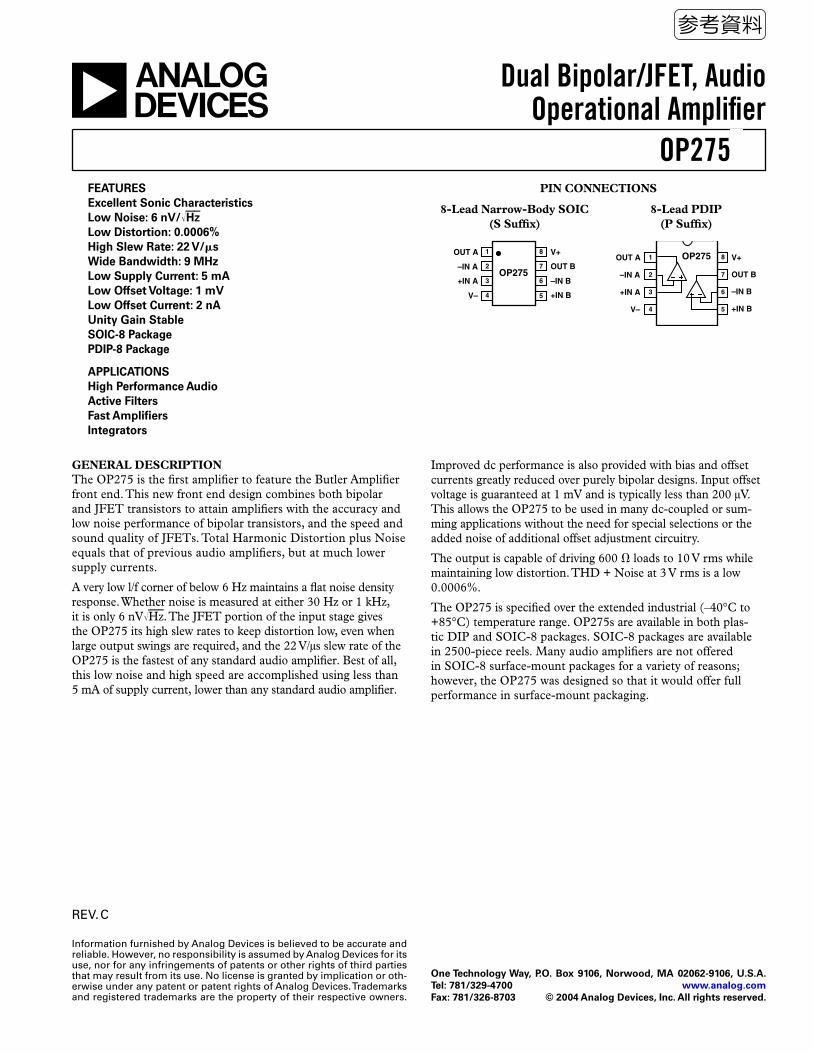
GENERAL DESCRIPTIONThe OP275 is the first amplifier to feature the Butler Amplifier front end. This new front end design combines both bipolar and JFET transistors to attain amplifiers with the accuracy and low noise performance of bipolar transistors, and the speed and sound quality of JFETs. Total Harmonic Distortion plus Noise equals that of previous audio amplifiers, but at much lower supply currents.
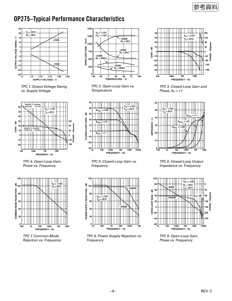
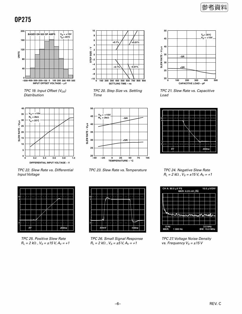
A very low l/f corner of below 6 Hz maintains a flat noise density response. Whether noise is measured at either 30 Hz or 1 kHz, it is only 6 nVHz. The JFET portion of the input stage gives the OP275 its high slew rates to keep distortion low, even when large output swings are required, and the 22 V/µs slew rate of the OP275 is the fastest of any standard audio amplifier. Best of all, this low noise and high speed are accomplished using less than 5 mA of supply current, lower than any standard audio amplifier.
Improved dc performance is also provided with bias and offset currents greatly reduced over purely bipolar designs. Input offset voltage is guaranteed at 1 mV and is typically less than 200 µV. This allows the OP275 to be used in many dc-coupled or sum-ming applications without the need for special selections or the added noise of additional offset adjustment circuitry.
The output is capable of driving 600 loads to 10 V rms while maintaining low distortion. THD + Noise at 3 V rms is a low 0.0006%.
The OP275 is specified over the extended industrial (–40°C to +85°C) temperature range. OP275s are available in both plas-tic DIP and SOIC-8 packages. SOIC-8 packages are available in 2500-piece reels. Many audio amplifiers are not offered in SOIC-8 surface-mount packages for a variety of reasons; however, the OP275 was designed so that it would offer full performance in surface-mount packaging.
ELECTRICAL CHARACTERISTICSParameter Symbol Conditions Min Typ Max Unit
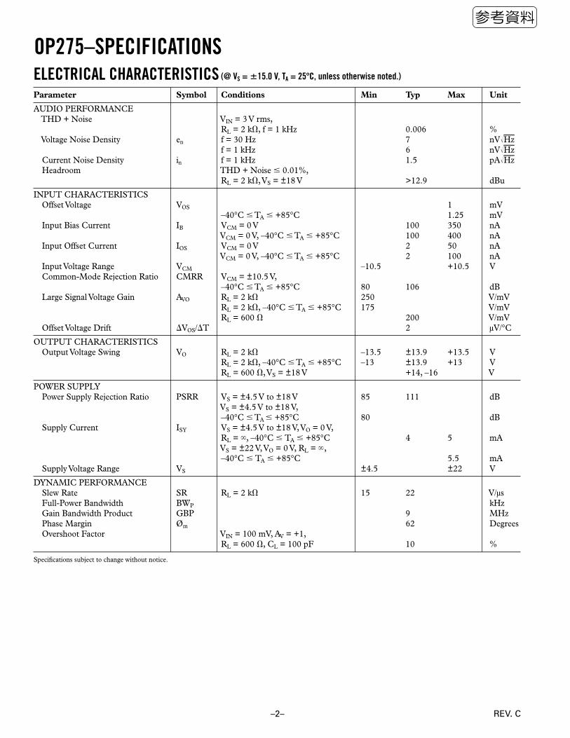
AUDIO PERFORMANCE THD + Noise VIN = 3 V rms, RL = 2 k, f = 1 kHz 0.006 % Voltage Noise Density en f = 30 Hz 7 nVHz f = 1 kHz 6 nVHz Current Noise Density in f = 1 kHz 1.5 pAHz Headroom THD + Noise 0.01%, RL = 2 k, VS = ±18 V >12.9 dBu
INPUT CHARACTERISTICS Offset Voltage VOS 1 mV –40°C TA +85°C 1.25 mV Input Bias Current IB VCM = 0 V 100 350 nA VCM = 0 V, –40°C TA +85°C 100 400 nA Input Offset Current IOS VCM = 0 V 2 50 nA VCM = 0 V, –40°C TA +85°C 2 100 nA Input Voltage Range VCM –10.5 +10.5 V Common-Mode Rejection Ratio CMRR VCM = ±10.5 V, –40°C TA +85°C 80 106 dB Large Signal Voltage Gain AVO RL = 2 k 250 V/mV RL = 2 k, –40°C TA +85°C 175 V/mV RL = 600 200 V/mV Offset Voltage Drift VOS/T 2 µV/°C
OUTPUT CHARACTERISTICS Output Voltage Swing VO RL = 2 k –13.5 ±13.9 +13.5 V RL = 2 k, –40°C TA +85°C –13 ±13.9 +13 V RL = 600 , VS = ±18 V +14, –16 V
POWER SUPPLY Power Supply Rejection Ratio PSRR VS = ±4.5 V to ±18 V 85 111 dB VS = ±4.5 V to ±18 V, –40°C TA +85°C 80 dB Supply Current ISY VS = ±4.5 V to ±18 V, VO = 0 V, RL = , –40°C TA +85°C 4 5 mA VS = ±22 V, VO = 0 V, RL = , –40°C TA +85°C 5.5 mA Supply Voltage Range VS ±4.5 ±22 V
NOTES1Absolute maximum ratings apply to packaged parts, unless otherwise noted.2For supply voltages greater than ±22 V, the absolute maximum input voltage is equal to the supply voltage.
3Shorts to either supply may destroy the device. See data sheet for full details.4JA is specified for the worst-case conditions, i.e., JA is specified for device in socket for PDIP packages; JA is specified for device soldered in circuit board for SOIC packages.
ORDERING GUIDE
Model Temperature Range Package Description Package Option
OP275GP –40°C to +85°C 8-Lead PDIP N-8OP275GS –40°C to +85°C 8-Lead SOIC R-8OP275GS-REEL –40°C to +85°C 8-Lead SOIC R-8OP275GS-REEL7 –40°C to +85°C 8-Lead SOIC R-8OP275GSZ* –40°C to +85°C 8-Lead SOIC R-8OP275GSZ-REEL* –40°C to +85°C 8-Lead SOIC R-8OP275GSZ-REEL7* –40°C to +85°C 8-Lead SOIC R-8*Z = Pb-free part.
CAUTIONESD (electrostatic discharge) sensitive device. Electrostatic charges as high as 4000 V readily accumulate on the human body and test equipment and can discharge without detection. Although the OP275 features proprietary ESD protection circuitry, permanent damage may occur on devices subjected to high energy electrostatic discharges. Therefore, proper ESD precautions are recommended to avoid performance degradation or loss of functionality.
REV. C REV. C
参考資料
–4–
OP275–Typical Performance Characteristics OP275
–5–
SUPPLY VOLTAGE – V
OU
TP
UT
VO
LT
AG
E S
WIN
G –
V
25
20
–250 5 2510 15 20
–5
–10
–15
–20
15
5
10
0
TA = 25C RL = 2k
+VOM
–VOM
TPC 1. Output Voltage Swing vs. Supply Voltage
FREQUENCY – Hz
1M 10M10k 100k
PH
AS
E –
De
gre
es
135
90
45
0
–45
–90
60
50
–20
40
30
20
10
0
–10
GA
IN –
dB
VS = 15V
TA = 25C
MARKER 15 309.059Hz MAG (A/H) 60.115dB
MARKER 15 309.058Hz PHASE (A/R) 90.606Deg
TPC 4. Open-Loop Gain, Phase vs. Frequency
FREQUENCY – Hz
120
100
0100 1k 10M10k 100k 1M
80
60
40
20
VS = 15V TA = 25C
CO
MM
ON
-MO
DE
RE
JEC
TIO
N –
dB
TPC 7. Common-Mode Rejection vs. Frequency
TEMPERATURE – C
OP
EN
-LO
OP
GA
IN –
V/m
V
1500
0–50 –25 1000 25 50 75
1250
1000
750
500
250
VS = 15V VO = 15V
+GAIN RL = 2k
–GAIN RL = 2k
+GAIN RL = 600
–GAIN RL = 600
TPC 2. Open-Loop Gain vs. Temperature
FREQUENCY – Hz
50
CL
OS
ED
-LO
OP
GA
IN –
dB
40
–301k 10k 100M100k 1M 10M
30
20
10
0
–10
–20
VS = 15V TA = 25C AVCL = +100
AVCL = +10
AVCL = +1
TPC 5. Closed-Loop Gain vs. Frequency
FREQUENCY – Hz
120
100
010 100 1M1k 10k 100k
80
60
40
20
PO
WE
R S
UP
PL
Y R
EJE
CT
ION
– d
B
VS = 15V TA = 25C
+PSRR
–PSRR
TPC 8. Power Supply Rejection vs. Frequency
FREQUENCY – Hz
1M 10M10k 100k
PH
AS
E –
Deg
rees
180
135
–180
90
45
0
–45
–90
–135
40
30
–40
20
10
0
–10
–20
–30
GA
IN –
dB
VS = 15V
TA = 25C
TPC 3. Closed-Loop Gain and Phase, AV = +1
FREQUENCY – Hz
60
IMP
ED
AN
CE
–
50
0100 1k 10M10k 100k 1M
40
30
20
10
VS = 15V TA = 25C
AVCL = +1
AVCL = +10
AVCL = +100
TPC 6. Closed-Loop Output Impedance vs. Frequency
FREQUENCY – Hz
100
80
–601k 10k 100M100k 1M 10M
60
40
20
0
–20
–40
0
PH
AS
E –
Deg
rees
45
90
135
180
225
270
VS = 15V RL = 2k
TA = 25C
OP
EN
-LO
OP
GA
IN –
dB
GAIN
PHASE Øm= 58
TPC 9. Open-Loop Gain, Phase vs. Frequency
REV. C REV. C
参考資料
–4–
OP275–Typical Performance Characteristics OP275
–5–
TEMPERATURE – C
GA
IN B
AN
DW
IDT
H P
RO
DU
CT
– M
Hz
11
10
7–50 –25 1000 25 50 75
9
8
PH
AS
E M
AR
GIN
– D
egre
es
65
60
40
55
50
GBW
Øm
TPC 10. Gain Bandwidth Product, Phase Margin vs. Temperature
25
20
15
10
5
FREQUENCY – Hz
MA
XIM
UM
OU
TP
UT
SW
ING
– V
30
01k 10k 10M100k 1M
TA = 25C VS = 15V AVCL = +1 RL = 2k
TPC 13. Maximum Output Swing vs. Frequency
TEMPERATURE – C
300
INP
UT
BIA
S C
UR
RE
NT
– n
A
0–50 –25 1000 25 50 75
250
200
150
100
50
VS = ±15V
TPC 16. Input Bias Current vs. Temperature
LOAD CAPACITANCE – pF
100
OV
ER
SH
OO
T –
%
90
00 100 500200 300 400
40
30
20
10
80
60
70
50
AVCL = +1 NEGATIVE EDGE
AVCL = +1 POSITIVE EDGE
VS = 15V
RL = 2k
VIN = 100mV p-p
TPC 11. Small Signal Overshoot vs. Load Capacitance
SUPPLY VOLTAGE – V
5.0
SU
PP
LY
CU
RR
EN
T –
mA 4.5
3.00 5 2510 15
4.0
3.5
20
TA = +25C
TA = –40C
TA = +85C
TPC 14. Supply Current vs. Supply Voltage
FREQUENCY – Hz10 100 100k1k
5
4
3
2
1
CU
RR
EN
T N
OIS
E D
EN
SIT
Y –
pA
/ H
z V = 15VT = 25C
S
A
TPC 17. Current Noise Density vs. Frequency
16
8
0100 1k 10k
2
4
6
10
12
14
LOAD RESISTANCE –
TA = 25CVS = 15V
+VOM
–VOM
MA
XIM
UM
OU
TP
UT
SW
ING
– V
TPC 12. Maximum Output Voltage vs. Load Resistance
TEMPERATURE – C
AB
SO
LU
TE
OU
TP
UT
CU
RR
EN
T –
mA
120
20–50 –25 1000 25 50 75
110
70
60
50
30
100
90
80
40
VS = 15V
SINK
SOURCE
TPC 15. Short-Circuit Current vs. Temperature
TCVOS – V/C
UN
ITS
500
400
00 1 102 3 4 5 6 7 8 9
300
200
100
BASED ON 920 OP AMPS
VS = 15V
–40C to +85C
TPC 18. TCVOS Distribution
REV. C REV. C
参考資料
–6–
OP275 OP275
–7–
INPUT OFFSET VOLTAGE – V
UN
ITS
200
160
0–500–400 500–300–200–100 0 100 200 300 400
120
80
40
BASED ON 920 OP AMPS VS = 15V TA = 25C
TPC 19. Input Offset (VOS) Distribution
DIFFERENTIAL INPUT VOLTAGE – V
40
20
00 1.0
35
30
10
5
25
15
SL
EW
RA
TE
– V
/s
VS = 15V
RL = 2k
TA = 25C
0.80.60.40.2
TPC 22. Slew Rate vs. Differential Input Voltage
10
0%
100
90
200ns5V
TPC 25. Positive Slew RateRL = 2 k , VS = ±15 V, AV = +1
SETTLING TIME – ns
ST
EP
SIZ
E –
V
10
8
–10
–2
–4
–6
–8
6
2
4
0
0 100 900200 300 400 500 600 700 800
+0.1% +0.01%
–0.1% –0.01%
TPC 20. Step Size vs. Settling Time
TEMPERATURE – C
50
SLE
W R
ATE
– V
/s
20–50 –25 1000 25 50 75
45
40
35
30
25
–SR
+SR
VS = 15V RL = 2k
TPC 23. Slew Rate vs. Temperature
10
0%
100
90
100ns50mV
TPC 26. Small Signal ResponseRL = 2 k , VS = ±5 V, AV = +1
+SR
–SR
CAPACITIVE LOAD – pF
50
45
SL
EW
RA
TE
– V
/s
200 100 500200 300 400
40
35
30
25
TA = 25CVS = 15V
TPC 21. Slew Rate vs. Capacitive Load
10
0%
100
90
200ns5V
TPC 24. Negative Slew RateRL = 2 k , VS = ±15 V, AV = +1
2.5 kHz0 Hz
CH A: 80.0 V FS 10.0 V/DIVMKR: 6.23 nV/ Hz
BW: 15.0 MHzMKR: 1 000 Hz
TPC 27. Voltage Noise Density vs. Frequency VS = ±15 V
REV. C REV. C
参考資料
–6–
OP275 OP275
–7–
APPLICATIONSCircuit ProtectionOP275 has been designed with inherent short-circuit protection to ground. An internal 30 resistor, in series with the output, limits the output current at room temperature to ISC+ = 40 mA and ISC– = –90 mA, typically, with ±15 V supplies.
However, shorts to either supply may destroy the device when excessive voltages or currents are applied. If it is possible for a user to short an output to a supply for safe operation, the output current of the OP275 should be design-limited to ±30 mA, as shown in Figure 1.
Total Harmonic DistortionTotal Harmonic Distortion + Noise (THD + N) of the OP275 is well below 0.001% with any load down to 600 . However, this is dependent upon the peak output swing. In Figure 2, the THD + Noise with 3 V rms output is below 0.001%. In Figure 3, THD + Noise is below 0.001% for the 10 k and 2 k loads but increases to above 0.1% for the 600 load condition. This is a result of the output swing capability of the OP275. Notice the results in Figure 4, showing THD versus VIN (V rms). This figure shows that the THD + Noise remains very low until the output reaches 9.5 V rms. This performance is similar to competitive products.
Figure 4. Headroom, THD + Noise vs. Output Amplitude (V rms); RLOAD = 600 , VSUP = ±18 V
The output of the OP275 is designed to maintain low harmonic distortion while driving 600 loads. However, driving 600 loads with very high output swings results in higher distortion if clipping occurs. A common example of this is in attempting to drive 10 V rms into any load with ±15 V supplies. Clipping will occur and distortion will be very high. To attain low harmonic distortion with large output swings, supply voltages may be increased. Figure 5 shows the performance of the OP275 driving 600 loads with supply voltages varying from ±18 V to ±20 V. Notice that with ±18 V supplies the distortion is fairly high, while with ±20 V supplies it is a very low 0.0007%.
SUPPLY VOLTAGE – V
0.0001
0.001
TH
D –
%
017 2218 19 20 21
0.01
0.1
RL = 600 VOUT = 10V rms @ 1kHz
Figure 5. THD + Noise vs. Supply Voltage
NoiseThe voltage noise density of the OP275 is below 7 nV/Hz from 30 Hz. This enables low noise designs to have good performance throughout the full audio range. Figure 6 shows a typical OP275 with a 1/f corner at 2.24 Hz.
10Hz0Hz
CH A: 80.0V FS 10.0V/DIVMKR: 45.6V/ Hz
BW: 0.145HzMKR: 2.24Hz
Figure 6. 1/f Noise Corner, VS = ±15 V, AV = 1000
REV. C REV. C
参考資料
OP275
–8–
OP275
–9–
Noise TestingFor audio applications, the noise density is usually the most important noise parameter. For characterization, the OP275 is tested using an Audio Precision, System One. The input signal to the Audio Precision must be amplified enough to measure it accurately. For the OP275, the noise is gained by approximately 1020 using the circuit shown in Figure 7. Any readings on the Audio Precision must then be divided by the gain. In imple-menting this test fixture, good supply bypassing is essential.
A
B
OP275
909
100
OP37
909100
909
100
OP37
4.42k
490
OUTPUT
Figure 7. Noise Test Fixture
Input Overcurrent ProtectionThe maximum input differential voltage that can be applied to the OP275 is determined by a pair of internal Zener diodes connected across its inputs. They limit the maximum differential input voltage to ±7.5 V. This is to prevent emitter-base junction breakdown from occurring in the input stage of the OP275 when very large differential voltages are applied. However, to preserve the OP275’s low input noise voltage, internal resistances in series with the inputs were not used to limit the current in the clamp diodes. In small signal applications, this is not an issue; however, in applications where large differential voltages can be inadvert-ently applied to the device, large transient currents can flow through these diodes. Although these diodes have been designed to carry a current of ±5 mA, external resistors as shown in Figure 8 should be used in the event that the OP275’s differential voltage were to exceed ±7.5 V.
OP275
1.4k
1.4k
–
+
2
3
6
Figure 8. Input Overcurrent Protection
Output Voltage Phase ReversalSince the OP275’s input stage combines bipolar transistors for low noise and p-channel JFETs for high speed performance, the output voltage of the OP275 may exhibit phase reversal if either of its inputs exceeds its negative common-mode input voltage. This might occur in very severe industrial applications where a sensor or system fault might apply very large voltages on the inputs of the OP275. Even though the input voltage range of the OP275 is ±10.5 V, an input voltage of approximately –13.5 V will cause output voltage phase reversal. In inverting amplifier con-figurations, the OP275’s internal 7.5 V input clamping diodes will
prevent phase reversal; however, they will not prevent this effect from occurring in noninverting applications. For these applications, the fix is a simple one and is illustrated in Figure 9. A 3.92 k resistor in series with the noninverting input of the OP275 cures the problem.
RFB*
VINRS
3.92k
VOUT
RL
2k
*RFB IS OPTIONAL
–
+
Figure 9. Output Voltage Phase Reversal Fix
Overload or Overdrive RecoveryOverload or overdrive recovery time of an operational amplifier is the time required for the output voltage to recover to a rated output voltage from a saturated condition. This recovery time is important in applications where the amplifier must recover quickly after a large abnormal transient event. The circuit shown in Figure 10 was used to evaluate the OP275’s overload recovery time. The OP275 takes approximately 1.2 ms to recover to VOUT = +10 V and approximately 1.5 µs to recover to VOUT = –10 V.
VIN
VOUT
RL
2.43k
A1 = 1/2 OP275
R210k
R11k
4V p-p@100Hz
1
2
3 A1
RS909k
–
+
Figure 10. Overload Recovery Time Test Circuit
Measuring Settling TimeThe design of OP275 combines a high slew rate and a wide gain bandwidth product to produce a fast settling (tS < 1 µs) amplifier for 8- and 12-bit applications. The test circuit designed to mea-sure the settling time of the OP275 is shown in Figure 11. This test method has advantages over false-sum node techniques in that the actual output of the amplifier is measured, instead of an error voltage at the sum node. Common-mode settling effects are exercised in this circuit in addition to the slew rate and band-width effects measured by the false-sum node method. Of course, a reasonably flat-top pulse is required as the stimulus.
The output waveform of the OP275 under test is clamped by Schottky diodes and buffered by the JFET source follower. The signal is amplified by a factor of 10 by the OP260 and then Schottky-clamped at the output to prevent overloading the oscilloscope’s input amplifier. The OP41 is configured as a fast integrator, which provides overall dc offset nulling.
High Speed OperationAs with most high speed amplifiers, care should be taken with supply decoupling, lead dress, and component placement. Recommended circuit configurations for inverting and nonin-verting applications are shown in Figures 12 and 13.
REV. C REV. C
参考資料
OP275
–8–
OP275
–9–
+15V
+0.1F
2
3
8
1
4VIN
VOUT
RL
2k
–15V
10F
0.1F
1/2OP275
10F
+
–
+
Figure 12. Unity Gain Follower
0.1F
+15V
+10F
2
3
8
1
4
VIN
VOUT
2k
–15V
10F0.1F
10pF
4.99k
2.49k
4.99k
+
1/2OP275
–
+
Figure 13. Unity Gain Inverter
In inverting and noninverting applications, the feedback resis-tance forms a pole with the source resistance and capacitance (RS and CS) and the OP275’s input capacitance (CIN), as shown in Figure 14. With RS and RF in the kilohm range, this pole can create excess phase shift and even oscillation. A small capacitor, CFB, in parallel and RFB eliminates this problem. By setting RS (CS + CIN) = RFBCFB, the effect of the feedback pole is completely removed.
16V–20V
0.1F
V+
5V
RL
1k
D1 D2
+15V
2N4416
1k
D3 D4
OUTPUT(TO SCOPE)
1F
10k
IC2
RF2k
7502N2222A
15k
–15V
1N4148
DUT 1/2 OP260AJ
16V–20V
0.1F
10k
– +
+ –
SCHOTTKY DIODES D1–D4 AREHEWLETT-PACKARD HP5082-2835IC1 IS 1/2 OP260AJIC2 IS PMI OP41EJ
V–
RG222
–
+
–
+–
+
Figure 11. OP275’s Settling Time Test Fixture
RFB
CINRS CS
CFB
VOUT
–
+
Figure 14. Compensating the Feedback Pole
Attention to Source Impedances Minimizes DistortionSince the OP275 is a very low distortion amplifier, careful atten-tion should be given to source impedances seen by both inputs. As with many FET-type amplifiers, the p-channel JFETs in the OP275’s input stage exhibit a gate-to-source capacitance that var-ies with the applied input voltage. In an inverting configuration, the inverting input is held at a virtual ground and, as such, does not vary with input voltage. Thus, since the gate-to-source voltage is constant, there is no distortion due to input capacitance modu-lation. In noninverting applications, however, the gate-to-source voltage is not constant. The resulting capacitance modulation can cause distortion above 1 kHz if the input impedance is greater than 2 k and unbalanced.
OP275
VIN
VOUT
RFRG
RS*
* RS = RG//RF IF RG//RF > 2k
FOR MINIMUM DISTORTION
–
+
Figure 15. Balanced Input Impedance to Minimize Distortion in Noninverting Amplifier Circuits
Figure 15 shows some guidelines for maximizing the distortion performance of the OP275 in noninverting applications. The best way to prevent unwanted distortion is to ensure that the parallel combination of the feedback and gain setting resistors (RF and RG) is less than 2 k. Keeping the values of these resistors small has the added benefits of reducing the thermal noise of the circuit
REV. C REV. C
参考資料
OP275
–10–
OP275
–11–
and dc offset errors. If the parallel combination of RF and RG is larger than 2 k, then an additional resistor, RS, should be used in series with the noninverting input. The value of RS is deter-mined by the parallel combination of RF and RG to maintain the low distortion performance of the OP275.
Driving Capacitive LoadsThe OP275 was designed to drive both resistive loads to 600 and capacitive loads of over 1000 pF and maintain stability. While there is a degradation in bandwidth when driving capacitive loads, the designer need not worry about device stability. The graph in Figure 16 shows the 0 dB bandwidth of the OP275 with capaci-tive loads from 10 pF to 1000 pF.
10
9
8
7
6
5
4
3
2
1
00 200 400 600 800 1000
CLOAD – pF
BA
ND
WID
TH
– M
Hz
Figure 16. Bandwidth vs. CLOAD
High Speed, Low Noise Differential Line DriverThe circuit in Figure 17 is a unique line driver widely used in industrial applications. With ±18 V supplies, the line driver can deliver a differential signal of 30 V p-p into a 2.5 k load. The high slew rate and wide bandwidth of the OP275 combine to yield a full power bandwidth of 130 kHz while the low noise front end produces a referred-to-input noise voltage spectral density of 10 nV/Hz.
12
3 A2
13
2 A1
5
67
A3
VIN
VO1
VO2
R32k
R950
R111k
P110k
R121kR10
50
R82k
R22k
R52k
R42k
R12k R7
2k
VO2 – VO1 = VIN
A1 = 1/2 OP275
A2, A3 = 1/2 OP275
GAIN =
SET R2, R4, R5 = R1 AND R6, R7, R8 = R3
R3R1
R62k
–
+
–
+
–
+
Figure 17. High Speed, Low Noise Differential Line Driver
The design is a transformerless, balanced transmission system where output common-mode rejection of noise is of paramount importance. Like the transformer based design, either output can be shorted to ground for unbalanced line driver applications without changing the circuit gain of 1. Other circuit gains can be set according to the equation in the diagram. This allows the design to be easily set to noninverting, inverting, or differential operation.
A 3-Pole, 40 kHz Low-Pass FilterThe closely matched and uniform ac characteristics of the OP275 make it ideal for use in GIC (Generalized Impedance Converter) and FDNR (Frequency-Dependent Negative Resistor) filter applications. The circuit in Figure 18 illustrates a linear-phase, 3-pole, 40 kHz low-pass filter using an OP275 as an inductance simulator (gyrator). The circuit uses one OP275 (A2 and A3) for the FDNR and one OP275 (A1 and A4) as an input buffer and bias current source for A3. Amplifier A4 is configured in a gain of 2 to set the pass band magnitude response to 0 dB. The ben-efits of this filter topology over classical approaches are that the op amp used in the FDNR is not in the signal path and that the filter’s performance is relatively insensitive to component varia-tions. Also, the configuration is such that large signal levels can be handled without overloading any of the filter’s internal nodes. As shown in Figure 19, the OP275’s symmetric slew rate and low distortion produce a clean, well behaved transient response.
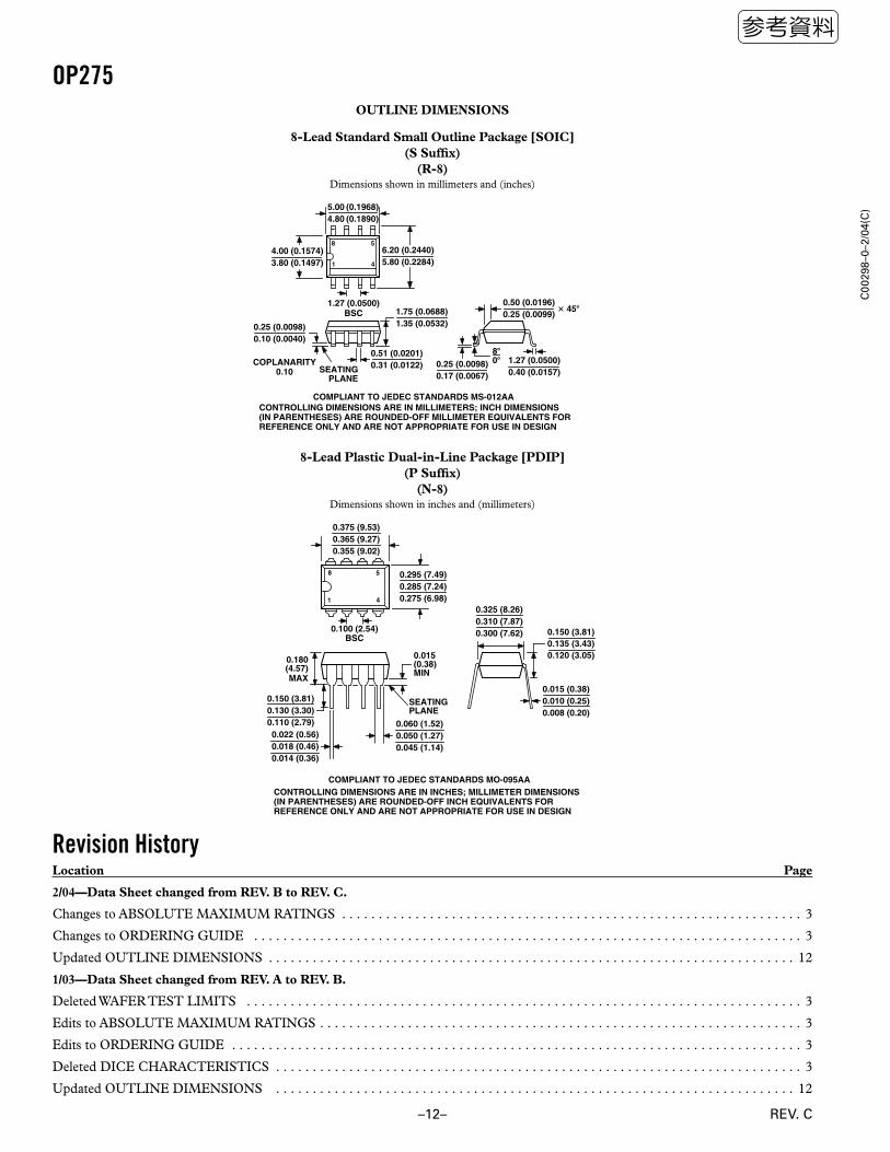
8-Lead Standard Small Outline Package [SOIC](S Suffix)
(R-8)Dimensions shown in millimeters and (inches)
0.25 (0.0098)0.17 (0.0067)
1.27 (0.0500)0.40 (0.0157)
0.50 (0.0196)0.25 (0.0099)
45
80
1.75 (0.0688)1.35 (0.0532)
SEATINGPLANE
0.25 (0.0098)0.10 (0.0040)
8 5
41
5.00 (0.1968)4.80 (0.1890)
4.00 (0.1574)3.80 (0.1497)
1.27 (0.0500)BSC
6.20 (0.2440)5.80 (0.2284)
0.51 (0.0201)0.31 (0.0122)COPLANARITY
0.10
CONTROLLING DIMENSIONS ARE IN MILLIMETERS; INCH DIMENSIONS(IN PARENTHESES) ARE ROUNDED-OFF MILLIMETER EQUIVALENTS FORREFERENCE ONLY AND ARE NOT APPROPRIATE FOR USE IN DESIGN
CONTROLLING DIMENSIONS ARE IN INCHES; MILLIMETER DIMENSIONS(IN PARENTHESES) ARE ROUNDED-OFF INCH EQUIVALENTS FORREFERENCE ONLY AND ARE NOT APPROPRIATE FOR USE IN DESIGN