94
EE 505 CMOS and BiCMOS Data Conversion Circuits
EE 505
CMOS and BiCMOS Data
Conversion Circuits

Course Information:
Lecture Instructor:
Randy Geiger
2133 Coover
Voice: 294-7745
e-mail: [email protected]
WEB: www.randygeiger.org
Laboratory Instructor:
Randy Geiger
Course Information:
CMOS and BiCMOS Data
Conversion Circuits
Lecture: MW 2:15-3:35
Online
Labs: W 8:00 – 10:50
Online
Course WEB Site: http://class.ee.iastate.edu/ee505/
Theory, design and applications of data conversion circuits (A/D and D/A
converters) including: architectures, characterization, quantization effects,
conversion algorithms, spectral performance, element matching, design for
yield, and practical comparators, implementation issues.
Course Description:

Course Information:Key Reference Texts:
Data Converters, Maloberti,
Springer, 2007Analog-to-Digital Conversion – 3rd
Edition by Marcel Pelgrom,
Springer, 2016
Course Information:Other Reference Texts:
Advanced Data Converters
by G. Manganaro, Cambridge,
2012
CMOS Integrated Analog-to-Digital
and Digital-to-Analog Converters –
2nd Edition by Rudy van de
Plassche, Kluwer, 2003
Course Information:Other Reference Texts:
Principles of Data Conversion
System Design
by B. Razavi, IEEE Press, 1995
High Speed Data Converters
by A. Ali, IET, 2016
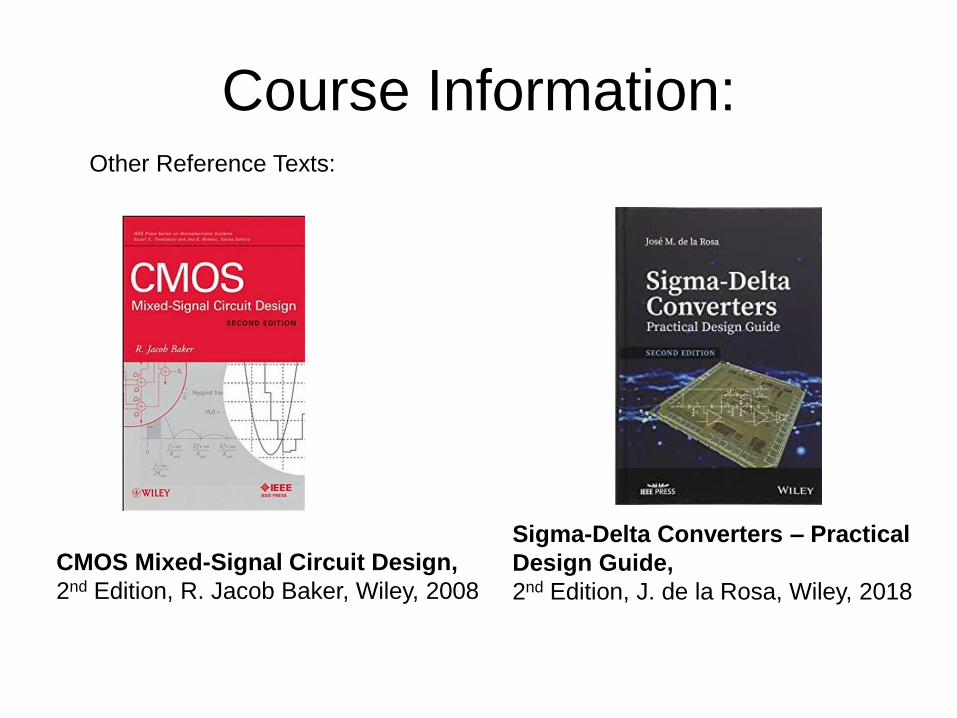
Course Information:Other Reference Texts:
CMOS Mixed-Signal Circuit Design,
2nd Edition, R. Jacob Baker, Wiley, 2008
Sigma-Delta Converters – Practical
Design Guide,
2nd Edition, J. de la Rosa, Wiley, 2018

Course Information:Other Reference Texts:
The Art of Analog Layout
by A. Hastings, Prentice Hall, 2001
Data Conversion Handbook
by Analog Devices, 2005
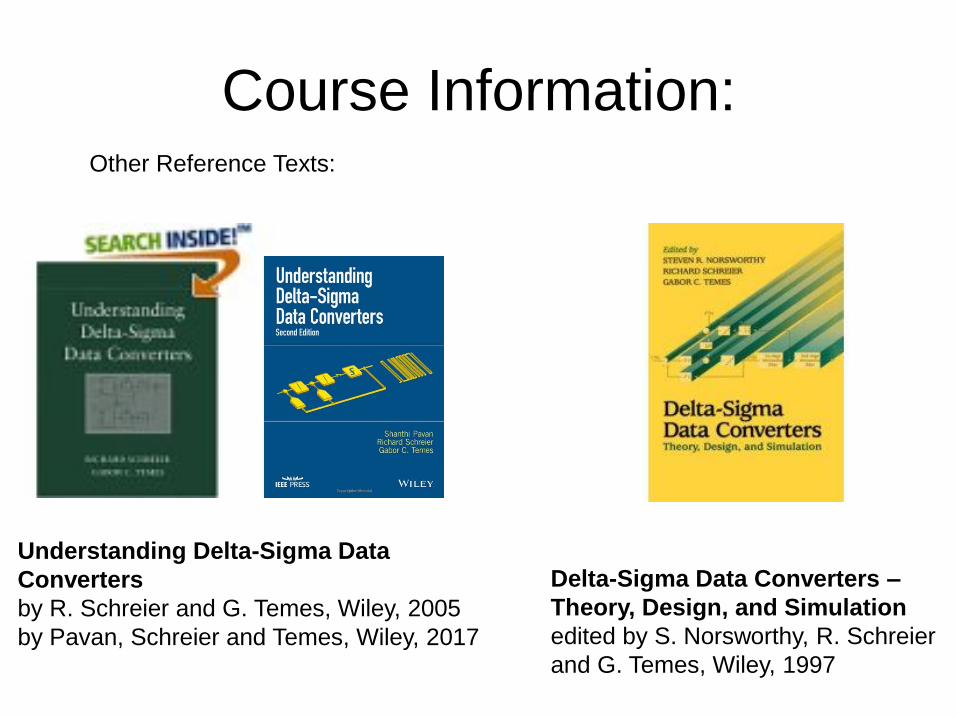
Course Information:Other Reference Texts:
Understanding Delta-Sigma Data
Converters
by R. Schreier and G. Temes, Wiley, 2005
by Pavan, Schreier and Temes, Wiley, 2017
Delta-Sigma Data Converters –
Theory, Design, and Simulation
edited by S. Norsworthy, R. Schreier
and G. Temes, Wiley, 1997
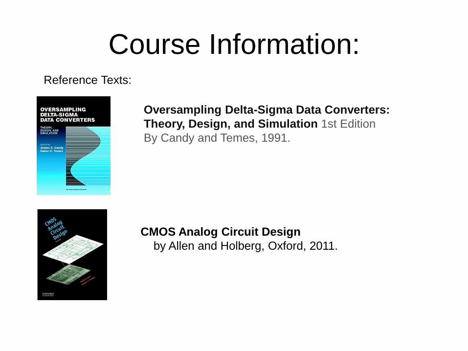
Course Information:Reference Texts:
CMOS Analog Circuit Design
by Allen and Holberg, Oxford, 2011.
Oversampling Delta-Sigma Data Converters:
Theory, Design, and Simulation 1st Edition
By Candy and Temes, 1991.
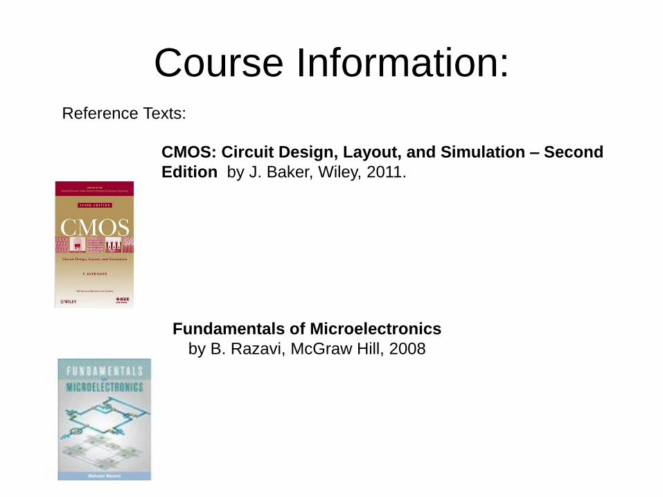
Course Information:Reference Texts:
CMOS: Circuit Design, Layout, and Simulation – Second
Edition by J. Baker, Wiley, 2011.
Fundamentals of Microelectronics
by B. Razavi, McGraw Hill, 2008
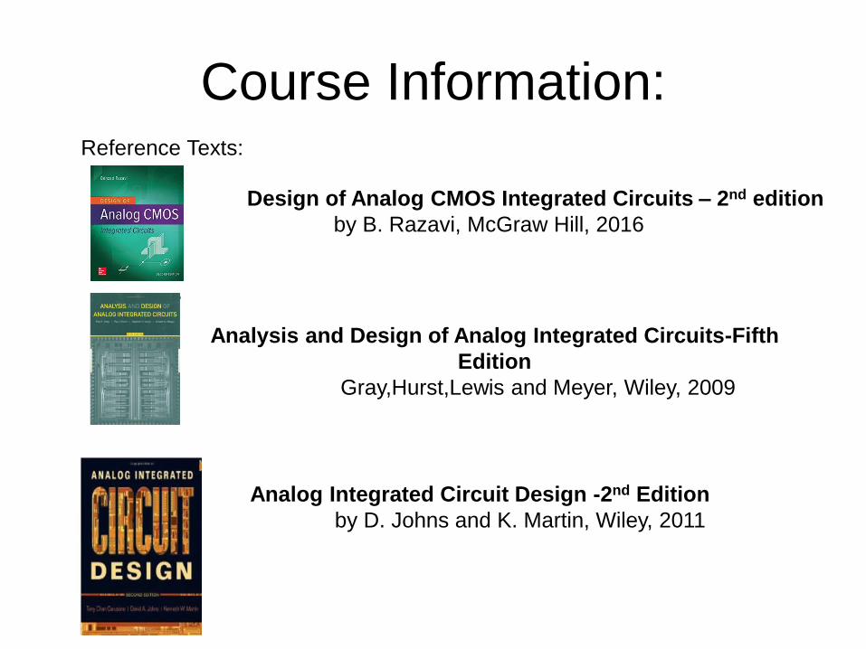
Course Information:Reference Texts:
Design of Analog CMOS Integrated Circuits – 2nd edition
by B. Razavi, McGraw Hill, 2016
Analysis and Design of Analog Integrated Circuits-Fifth
Edition
Gray,Hurst,Lewis and Meyer, Wiley, 2009
Analog Integrated Circuit Design -2nd Edition
by D. Johns and K. Martin, Wiley, 2011

Course Information:Reference Materials:

Course Information:
Grading: Points will be allocated for several different parts of the course. A
letter grade will be assigned based upon the total points accumulated. The
points allocated for different parts of the course are as listed below:
1 Exam 100 pts
1 Final 100 pts.
Homework 100 pts.total
Lab and Lab Reports 100 pts.total
Design Project 100 pts.
Note: In the event that one of the exams is not given, the weight of the remaining
exam will be increased to somewhere between 100 pts and 200 pts.

Course Information:
Design Project:
The design project will be assigned by mid-term. Additional details
about the design project will be given after relevant material is covered in class.
The option will exist to have this project fabricated through the MOSIS program.
The design should be ready for fabrication and post-layout simulations are to
be included as a part of the project.

Course Information:
E-MAIL:
I encourage you to take advantage of the e-mail system on campus to
communicate about any issues that arise in the course. I typically check my e-
mail several times a day. Please try to include “EE 505" in the subject field of
any e-mail message that you send so that they stand out from what is often
large volumes of routine e-mail messages.
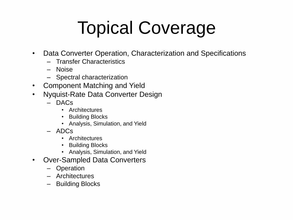
Topical Coverage
• Data Converter Operation, Characterization and Specifications– Transfer Characteristics
– Noise
– Spectral characterization
• Component Matching and Yield
• Nyquist-Rate Data Converter Design– DACs
• Architectures
• Building Blocks
• Analysis, Simulation, and Yield
– ADCs• Architectures
• Building Blocks
• Analysis, Simulation, and Yield
• Over-Sampled Data Converters– Operation
– Architectures
– Building Blocks
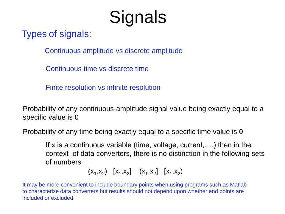
Types of signals:
Continuous amplitude vs discrete amplitude
Continuous time vs discrete time
Signals
Finite resolution vs infinite resolution
Probability of any continuous-amplitude signal value being exactly equal to a
specific value is 0
Probability of any time being exactly equal to a specific time value is 0
(x1,x2) [x1,x2] (x1,x2] [x1,x2)
If x is a continuous variable (time, voltage, current,….) then in the
context of data converters, there is no distinction in the following sets
of numbers
It may be more convenient to include boundary points when using programs such as Matlab
to characterize data converters but results should not depend upon whether end points are
included or excluded
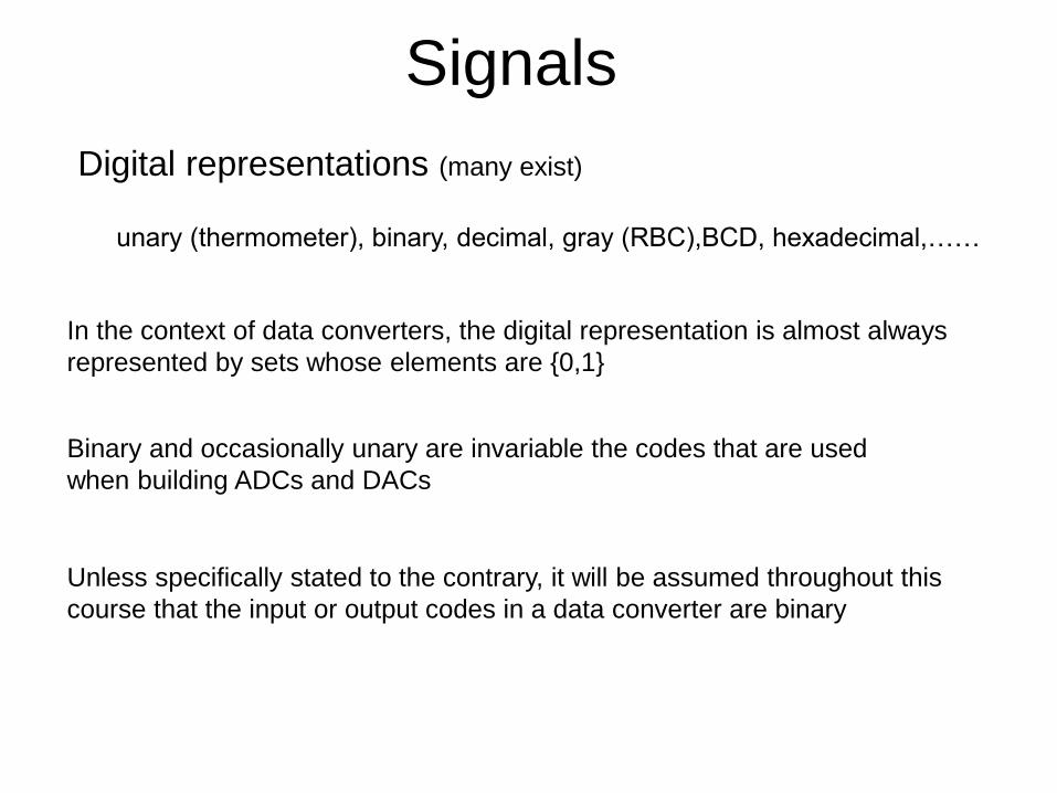
Digital representations (many exist)
Signals
unary (thermometer), binary, decimal, gray (RBC),BCD, hexadecimal,……
In the context of data converters, the digital representation is almost always
represented by sets whose elements are {0,1}
Binary and occasionally unary are invariable the codes that are used
when building ADCs and DACs
Unless specifically stated to the contrary, it will be assumed throughout this
course that the input or output codes in a data converter are binary
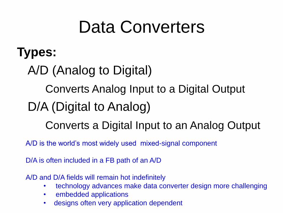
Data Converters
Types:
A/D (Analog to Digital)
Converts Analog Input to a Digital Output
D/A (Digital to Analog)
Converts a Digital Input to an Analog Output
A/D is the world’s most widely used mixed-signal component
D/A is often included in a FB path of an A/D
A/D and D/A fields will remain hot indefinitely
• technology advances make data converter design more challenging
• embedded applications
• designs often very application dependent
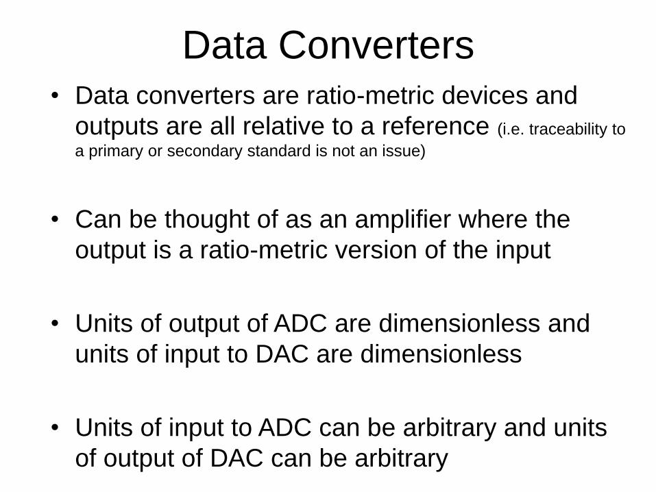
Data Converters • Data converters are ratio-metric devices and
outputs are all relative to a reference (i.e. traceability to
a primary or secondary standard is not an issue)
• Can be thought of as an amplifier where the
output is a ratio-metric version of the input
• Units of output of ADC are dimensionless and
units of input to DAC are dimensionless
• Units of input to ADC can be arbitrary and units
of output of DAC can be arbitrary
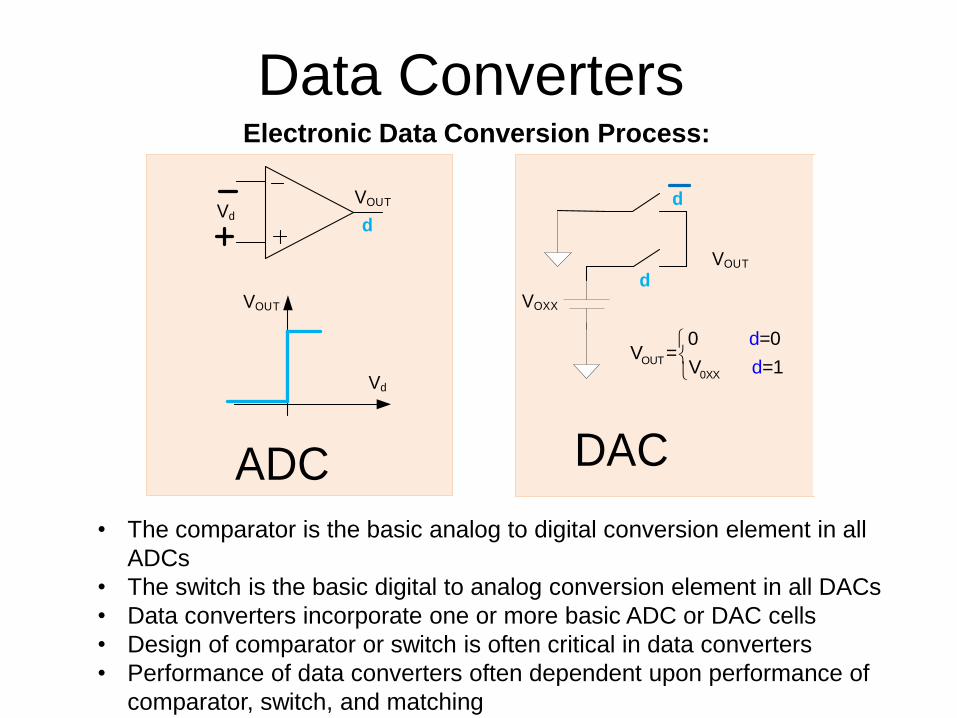
Data Converters Electronic Data Conversion Process:
VOUT
Vd
VOUTVd
d
VOUT
dVOXX
OUT
0XX
0 =0V =
V
d
d=1
ADC DAC
d
• The comparator is the basic analog to digital conversion element in all
ADCs
• The switch is the basic digital to analog conversion element in all DACs
• Data converters incorporate one or more basic ADC or DAC cells
• Design of comparator or switch is often critical in data converters
• Performance of data converters often dependent upon performance of
comparator, switch, and matching
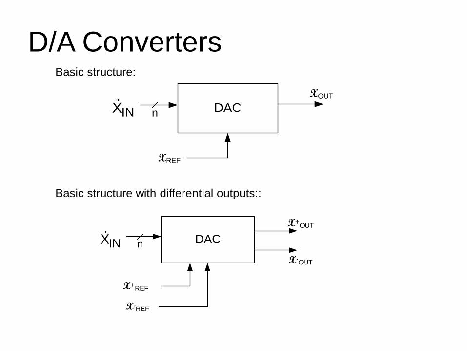
D/A Converters
nINX DACXOUT
XREF
nINX DAC
X+OUT
X+REF
X-REF
X-OUT
Basic structure:
Basic structure with differential outputs::
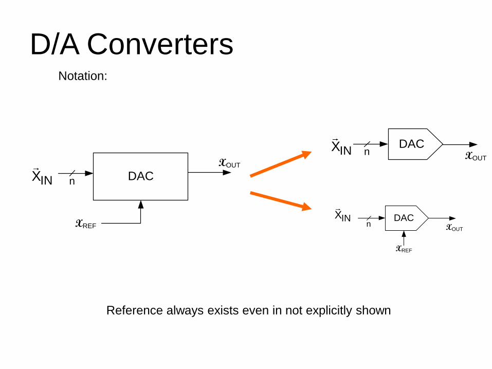
D/A Converters
nINX DACXOUT
XREF
Notation:
n XOUT
DACINX
n XOUT
DAC
XREF
INX
Reference always exists even in not explicitly shown
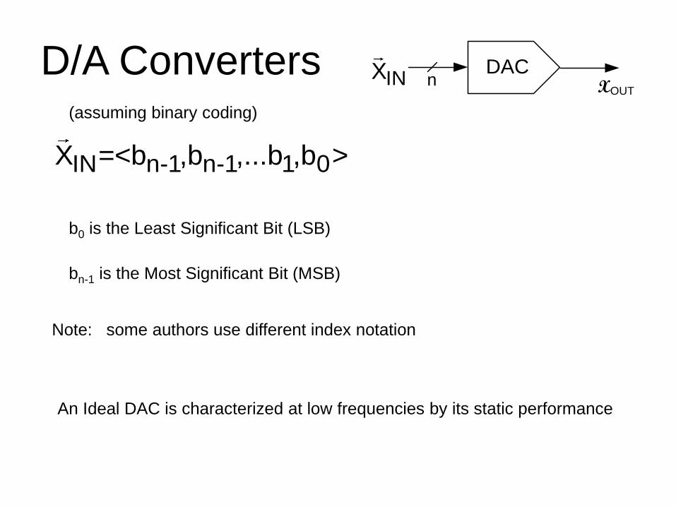
D/A Converters
IN n-1 n-1 1 0X =<b ,b ,...b ,b >
n XOUT
DACINX
b0 is the Least Significant Bit (LSB)
bn-1 is the Most Significant Bit (MSB)
Note: some authors use different index notation
An Ideal DAC is characterized at low frequencies by its static performance
(assuming binary coding)
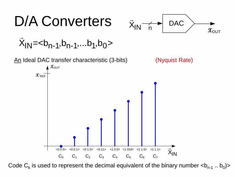
D/A Converters
IN n-1 n-1 1 0X =<b ,b ,...b ,b >
n XOUT
DACINX
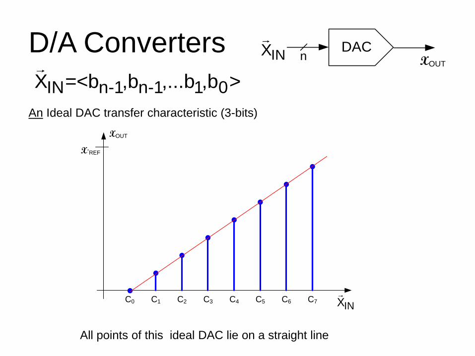
An Ideal DAC transfer characteristic (3-bits)
Code Ck is used to represent the decimal equivalent of the binary number <bn-1 .. b0)>
XOUT
<0 0 0> <0 0 1> <0 1 0> <0 11> <1 0 0> <1 010> <1 1 0> <1 1 1>
INXC0 C1 C2 C3 C4 C5 C6 C7
X-REF
(Nyquist Rate)
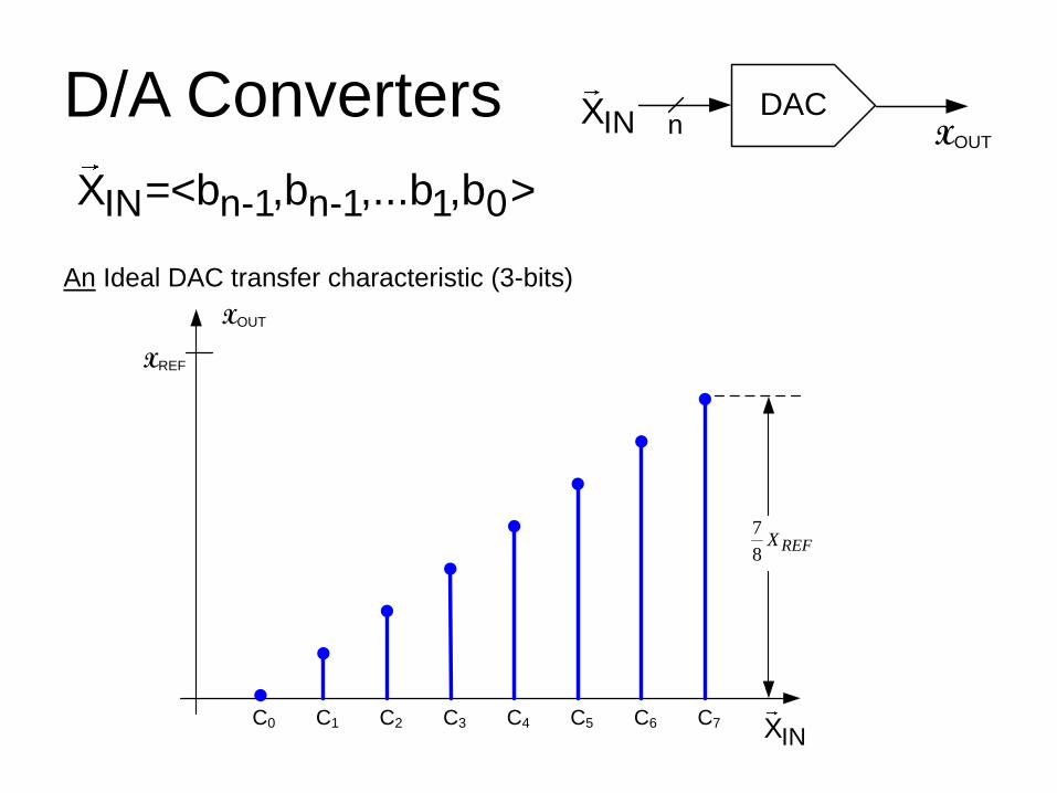
D/A Converters
IN n-1 n-1 1 0X =<b ,b ,...b ,b >
n XOUT
DACINX
An Ideal DAC transfer characteristic (3-bits)
XOUT
INX
7
8REFX
C0 C1 C2 C3 C4 C5 C6 C7
XREF
D/A Converters
IN n-1 n-1 1 0X =<b ,b ,...b ,b >
n XOUT
DACINX
An Ideal DAC transfer characteristic (3-bits)
All points of this ideal DAC lie on a straight line
XOUT
INXC0 C1 C2 C3 C4 C5 C6 C7
X-REF
D/A Convertersn XOUT
DACINX
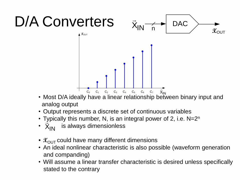
• Most D/A ideally have a linear relationship between binary input and
analog output
• Output represents a discrete set of continuous variables
• Typically this number, N, is an integral power of 2, i.e. N=2n
• is always dimensionless
• XOUT could have many different dimensions
• An ideal nonlinear characteristic is also possible (waveform generation
and companding)
• Will assume a linear transfer characteristic is desired unless specifically
stated to the contrary
INX
XOUT
INXC0 C1 C2 C3 C4 C5 C6 C7
D/A Convertersn XOUT
DACINX
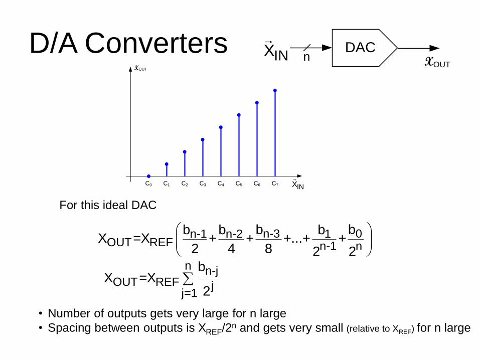
n-3 0n-1 n-2 1OUT REF n-1 n
b bb b bX =X + + +...+ +
2 4 8 2 2
For this ideal DAC
n n-jOUT REF j
j=1
bX =X
2
• Number of outputs gets very large for n large
• Spacing between outputs is XREF/2n and gets very small (relative to XREF) for n large
XOUT
INXC0 C1 C2 C3 C4 C5 C6 C7
D/A Convertersn XOUT
DACINX
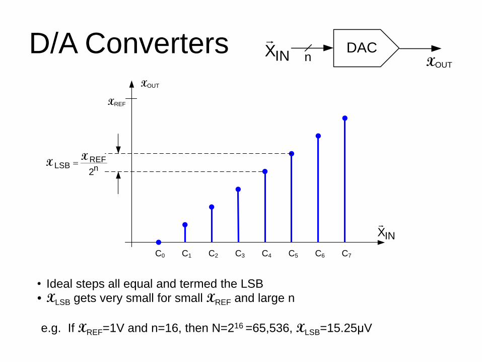
• Ideal steps all equal and termed the LSB
• XLSB gets very small for small XREF and large n
e.g. If XREF=1V and n=16, then N=216 =65,536, XLSB=15.25μV
XOUT
INX
REF LSB n2
X
X
C0 C1 C2 C3 C4 C5 C6 C7
XREF
D/A Convertersn XOUT
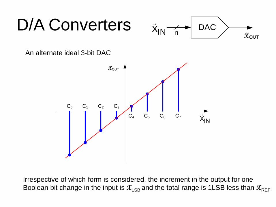
DACINX
An alternate ideal 3-bit DAC
Irrespective of which form is considered, the increment in the output for one
Boolean bit change in the input is XLSB and the total range is 1LSB less than XREF
XOUT
INX
C0 C1 C2 C3
C4 C5 C6 C7
Applications of DACs
• Waveform Generation
• Voltage Generation
• Analog Trim or Calibration
• Industrial Control Systems
• Feedback Element in ADCs
• ….
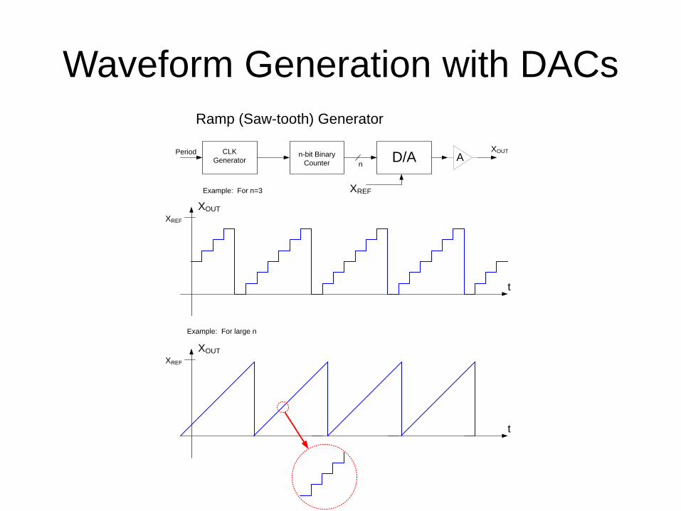
Waveform Generation with DACs
CLK
Generatorn-bit Binary
CounterD/A A
XOUTPeriod
n
Example: For n=3 XREF
XREF
XOUT
t
Example: For large n
XREF
XOUT
t
Ramp (Saw-tooth) Generator
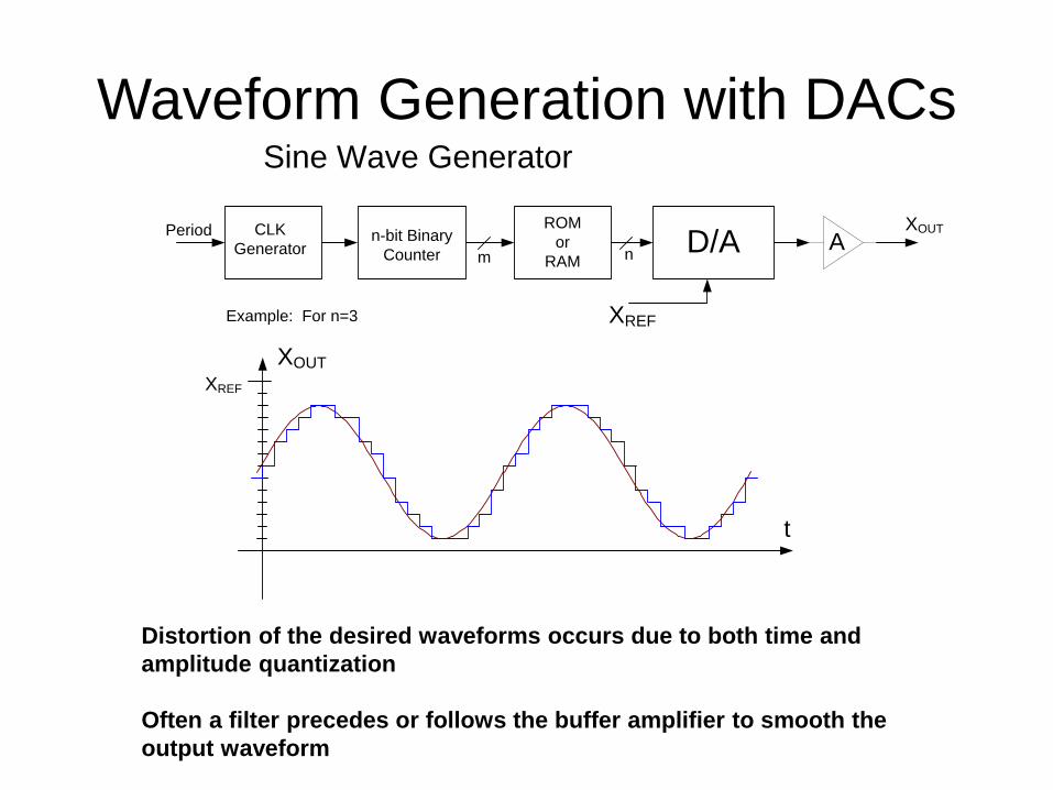
Waveform Generation with DACs
CLK
Generatorn-bit Binary
CounterD/A A
XOUTPeriod
m
Example: For n=3 XREF
XREF
XOUT
t
Sine Wave Generator
n
ROM
or
RAM
Distortion of the desired waveforms occurs due to both time and
amplitude quantization
Often a filter precedes or follows the buffer amplifier to smooth the
output waveform
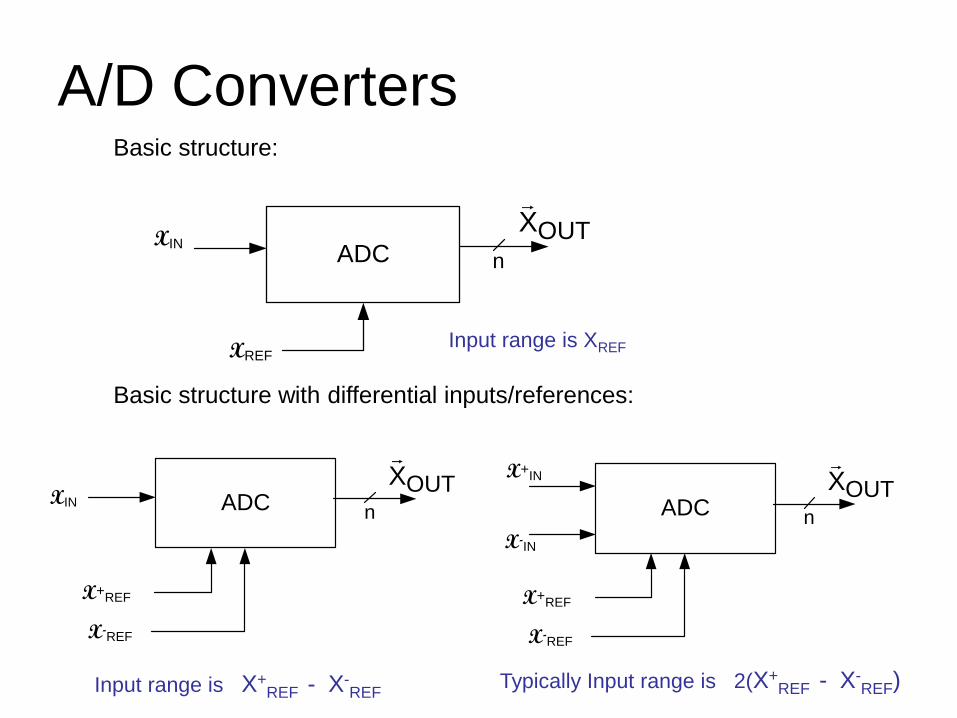
A/D ConvertersBasic structure:
Basic structure with differential inputs/references:
n
OUTXADC
XIN
XREF
ADC
X+REF
X-REF
n
OUTXXIN
X+IN
X-IN
ADC
X+REF
X-REF
n
OUTX
Input range is XREF
Input range is X+REF - X-
REFTypically Input range is 2(X+
REF - X-REF)
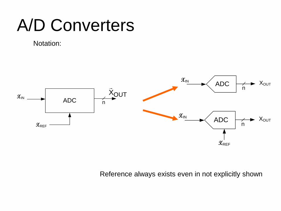
A/D ConvertersNotation:
n
OUTXADC
XIN
XREF
XINADC
nXOUT
XINADC
nXOUT
XREF
Reference always exists even in not explicitly shown
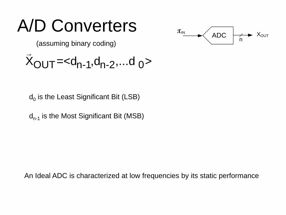
A/D Converters
OUT n-1 n-2 0X =<d ,d ,...d >
d0 is the Least Significant Bit (LSB)
dn-1 is the Most Significant Bit (MSB)
An Ideal ADC is characterized at low frequencies by its static performance
XINADC
nXOUT
(assuming binary coding)
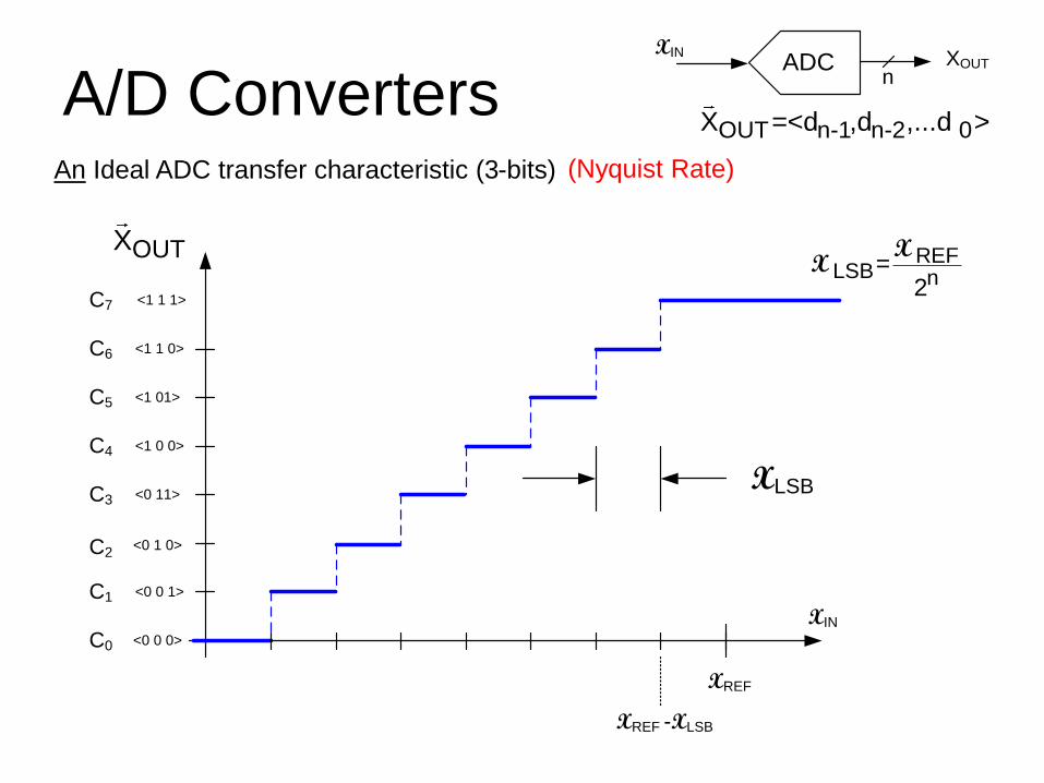
A/D ConvertersAn Ideal ADC transfer characteristic (3-bits)
XINADC
nXOUT
REF LSB n
=2
X X
XIN
<0 0 0>
<0 0 1>
<0 1 0>
<0 11>
<1 0 0>
<1 01>
<1 1 0>
<1 1 1>
OUTX
XREF
XLSB
XREF -XLSB
C0
C1
C2
C3
C4
C5
C6
C7
OUT n-1 n-2 0X =<d ,d ,...d >
(Nyquist Rate)
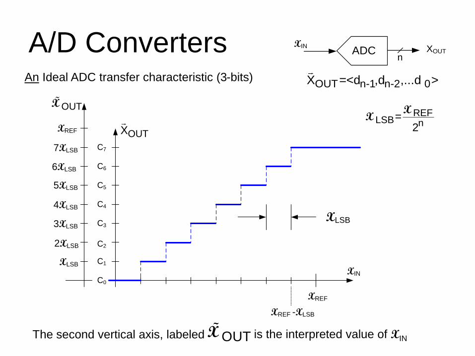
A/D ConvertersAn Ideal ADC transfer characteristic (3-bits)
XINADC
nXOUT
REF LSB n
=2
X X
OUTX is the interpreted value of XINThe second vertical axis, labeled
OUT n-1 n-2 0X =<d ,d ,...d >
XIN
OUTX
XREF
XLSB
XREF -XLSB
XREF
XLSB
2XLSB
3XLSB
4XLSB
5XLSB
6XLSB
7XLSB
OUTX
C0
C1
C2
C3
C4
C5
C6
C7
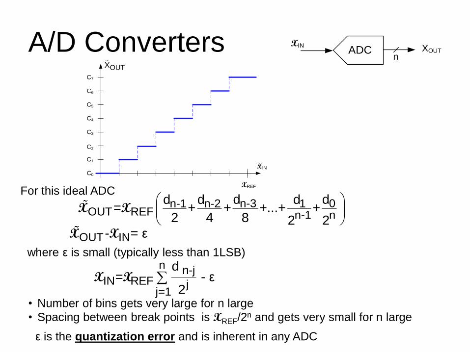
A/D Converters
n-3 0n-1 n-2 1OUT REF n-1 n
d dd d d= + + +...+ +
2 4 8 2 2
X X
For this ideal ADC
n n-jIN REF j
j=1
d= - ε
2X X
• Number of bins gets very large for n large
• Spacing between break points is XREF/2n and gets very small for n large
XINADC
nXOUT
where ε is small (typically less than 1LSB)
ε is the quantization error and is inherent in any ADC
XIN
OUTX
XREF
C0
C1
C2
C3
C4
C5
C6
C7
OUT IN- = εX X
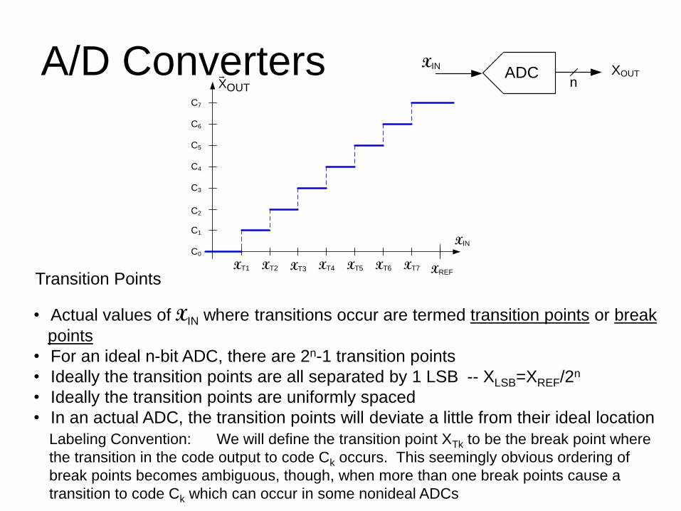
A/D Converters XINADC
nXOUT
Transition Points
XIN
OUTX
XREF
C0
C1
C2
C3
C4
C5
C6
C7
XT1 XT2 XT3 XT4 XT5 XT6 XT7
• Actual values of XIN where transitions occur are termed transition points or break
points
• For an ideal n-bit ADC, there are 2n-1 transition points
• Ideally the transition points are all separated by 1 LSB -- XLSB=XREF/2n
• Ideally the transition points are uniformly spaced
• In an actual ADC, the transition points will deviate a little from their ideal location
Labeling Convention: We will define the transition point XTk to be the break point where
the transition in the code output to code Ck occurs. This seemingly obvious ordering of
break points becomes ambiguous, though, when more than one break points cause a
transition to code Ck which can occur in some nonideal ADCs
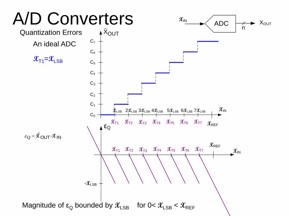
A/D Converters XINADC
nXOUT
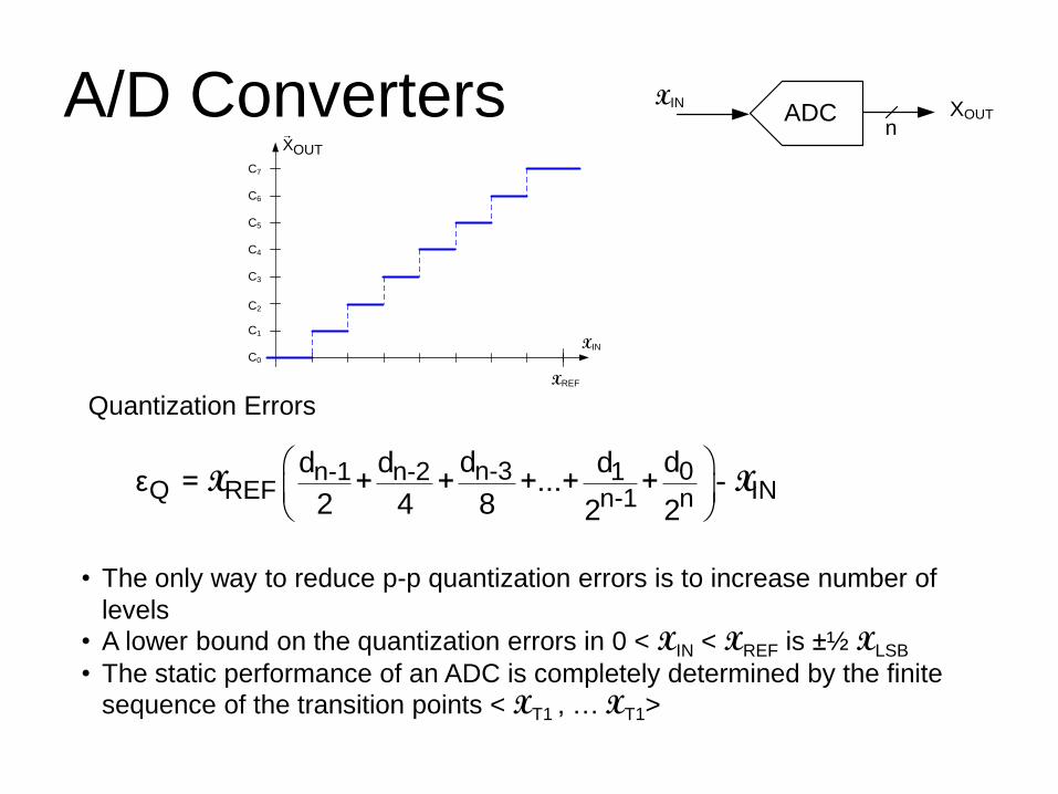
Quantization Errors
OUT IN-Q X X
XIN
εQ
-XLSB
XT2 XT3 XT4 XT5 XT6 XT7XT1
XREF
Magnitude of εQ bounded by XLSB for 0< XLSB < XREF
XT1=XLSB
XIN
OUTX
XREF
C0
C1
C2
C3
C4
C5
C6
C7
XT1 XT2 XT3 XT4 XT5 XT6 XT7
XLSB 2XLSB 3XLSB 4XLSB 5XLSB 6XLSB 7XLSB
An ideal ADC
A/D Converters XINADC
nXOUT
Quantization Errors
OUT IN-Q X X
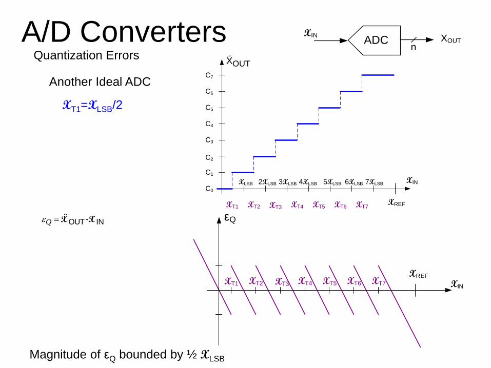
Magnitude of εQ bounded by ½ XLSB
Another Ideal ADC
XT1=XLSB/2
XIN
OUTX
XREF
C0
C1
C2
C3
C4
C5
C6
C7
XT1 XT2 XT3 XT4 XT5 XT6 XT7
XLSB 2XLSB 3XLSB 4XLSB 5XLSB 6XLSB 7XLSB
XIN
εQ
XT2 XT3 XT4 XT5 XT6 XT7XT1
XREF
A/D Converters
n-3 0n-1 n-2 1Q REF INn-1 n
d dd d dε = + + +...+ + -
2 4 8 2 2
X X
• The only way to reduce p-p quantization errors is to increase number of
levels
• A lower bound on the quantization errors in 0 < XIN < XREF is ±½ XLSB
• The static performance of an ADC is completely determined by the finite
sequence of the transition points < XT1 , … XT1>
XINADC
nXOUT
XIN
OUTX
XREF
C0
C1
C2
C3
C4
C5
C6
C7
Quantization Errors
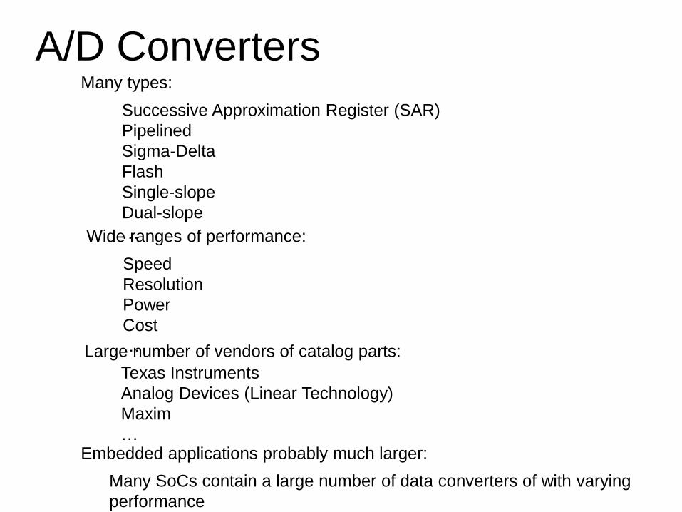
A/D ConvertersMany types:
Successive Approximation Register (SAR)
Pipelined
Sigma-Delta
Flash
Single-slope
Dual-slope
…Wide ranges of performance:
Speed
Resolution
Power
Cost
…Large number of vendors of catalog parts:
Texas Instruments
Analog Devices (Linear Technology)
Maxim
…Embedded applications probably much larger:
Many SoCs contain a large number of data converters of with varying
performance
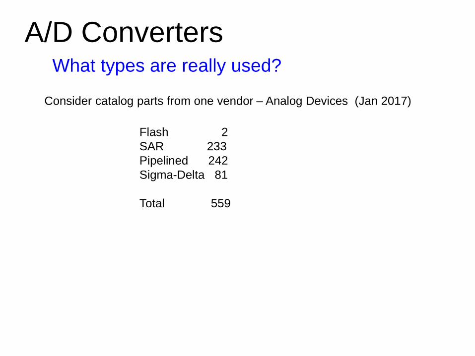
A/D ConvertersWhat types are really used?
Consider catalog parts from one vendor – Analog Devices (Jan 2017)
Flash 2
SAR 233
Pipelined 242
Sigma-Delta 81
Total 559
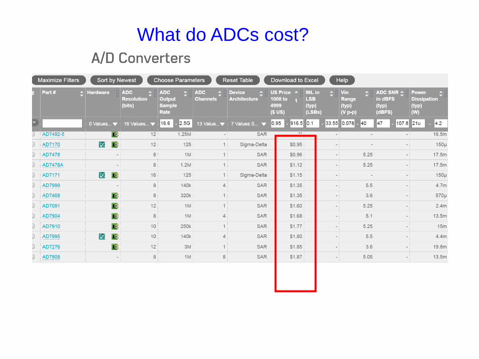
What do ADCs cost?
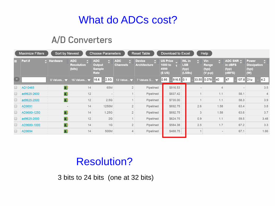
What do ADCs cost?
Resolution?
3 bits to 24 bits (one at 32 bits)
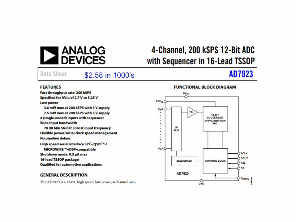
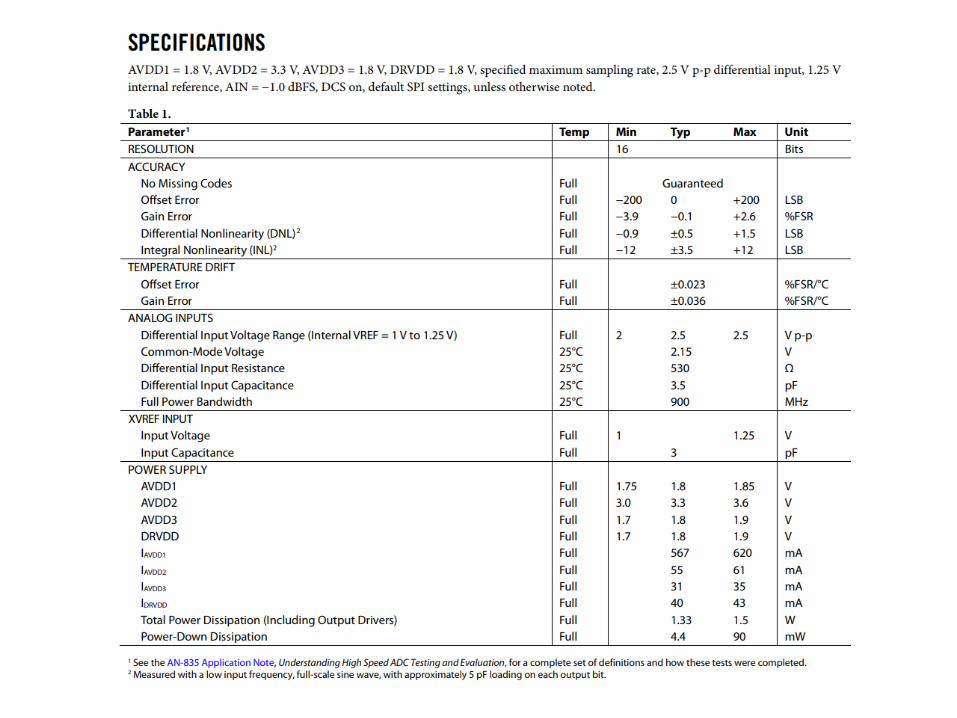
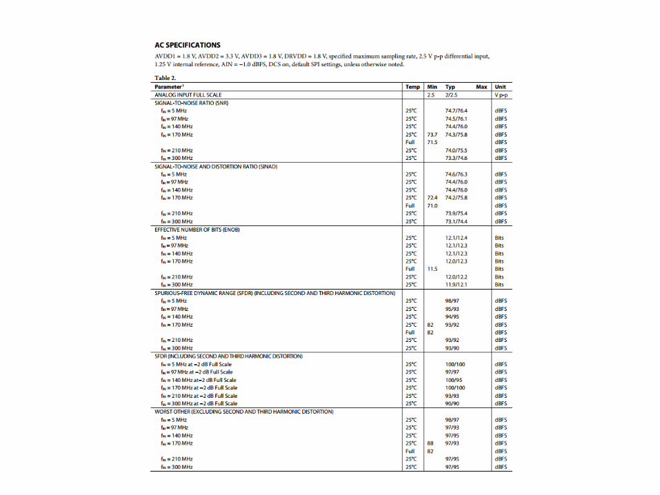
$2.58 in 1000’s
$120 in 1000’s
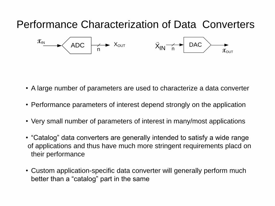
Performance Characterization of Data Converters
• A large number of parameters are used to characterize a data converter
• Performance parameters of interest depend strongly on the application
• Very small number of parameters of interest in many/most applications
• “Catalog” data converters are generally intended to satisfy a wide range
of applications and thus have much more stringent requirements placd on
their performance
• Custom application-specific data converter will generally perform much
better than a “catalog” part in the same
XINADC
nXOUT
n XOUT
DACINX
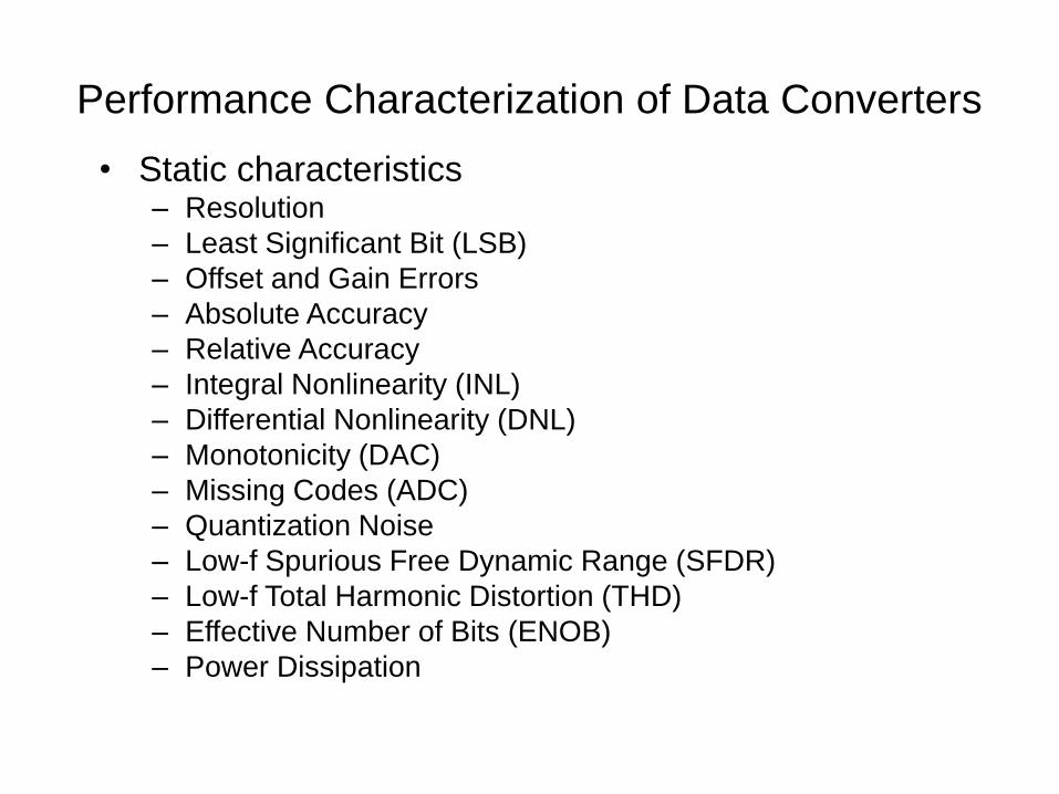
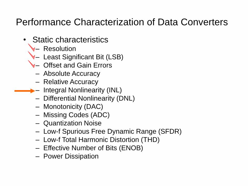
Performance Characterization of Data Converters
• Static characteristics– Resolution
– Least Significant Bit (LSB)
– Offset and Gain Errors
– Absolute Accuracy
– Relative Accuracy
– Integral Nonlinearity (INL)
– Differential Nonlinearity (DNL)
– Monotonicity (DAC)
– Missing Codes (ADC)
– Quantization Noise
– Low-f Spurious Free Dynamic Range (SFDR)
– Low-f Total Harmonic Distortion (THD)
– Effective Number of Bits (ENOB)
– Power Dissipation
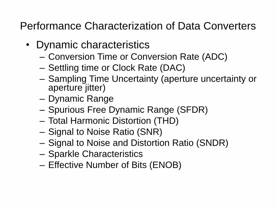
Performance Characterization of Data Converters
• Dynamic characteristics– Conversion Time or Conversion Rate (ADC)
– Settling time or Clock Rate (DAC)
– Sampling Time Uncertainty (aperture uncertainty or aperture jitter)
– Dynamic Range
– Spurious Free Dynamic Range (SFDR)
– Total Harmonic Distortion (THD)
– Signal to Noise Ratio (SNR)
– Signal to Noise and Distortion Ratio (SNDR)
– Sparkle Characteristics
– Effective Number of Bits (ENOB)
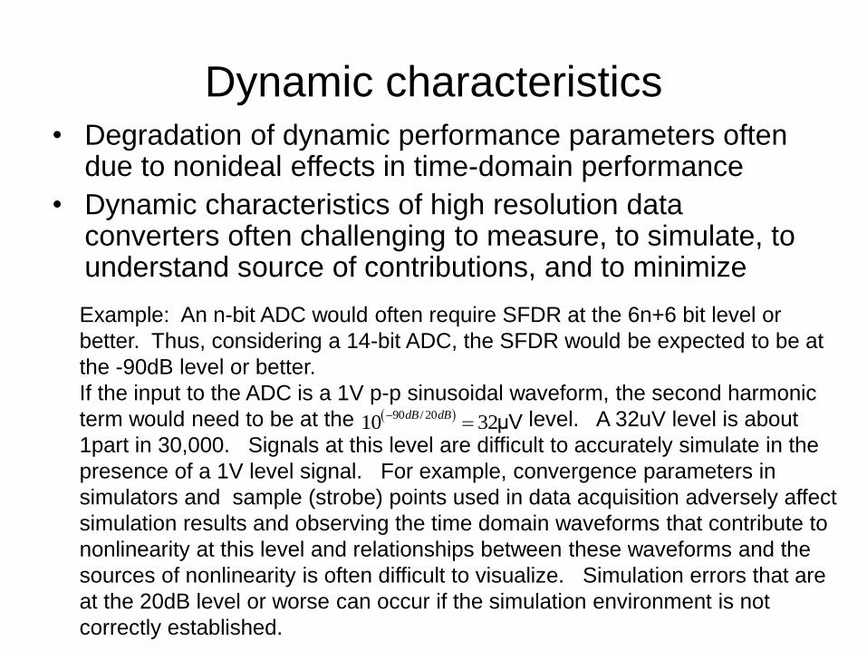
Dynamic characteristics• Degradation of dynamic performance parameters often
due to nonideal effects in time-domain performance
• Dynamic characteristics of high resolution data converters often challenging to measure, to simulate, to understand source of contributions, and to minimize
Example: An n-bit ADC would often require SFDR at the 6n+6 bit level or
better. Thus, considering a 14-bit ADC, the SFDR would be expected to be at
the -90dB level or better.
If the input to the ADC is a 1V p-p sinusoidal waveform, the second harmonic
term would need to be at the level. A 32uV level is about
1part in 30,000. Signals at this level are difficult to accurately simulate in the
presence of a 1V level signal. For example, convergence parameters in
simulators and sample (strobe) points used in data acquisition adversely affect
simulation results and observing the time domain waveforms that contribute to
nonlinearity at this level and relationships between these waveforms and the
sources of nonlinearity is often difficult to visualize. Simulation errors that are
at the 20dB level or worse can occur if the simulation environment is not
correctly established.
90 /2010 32μV
dB dB
Characterization of Data Converter
Performance
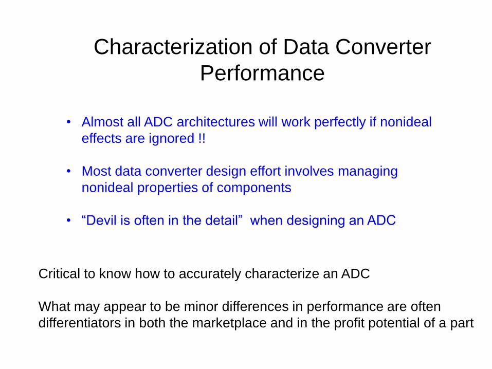
Critical to know how to accurately characterize an ADC
What may appear to be minor differences in performance are often
differentiators in both the marketplace and in the profit potential of a part
• Almost all ADC architectures will work perfectly if nonideal
effects are ignored !!
• Most data converter design effort involves managing
nonideal properties of components
• “Devil is often in the detail” when designing an ADC
Performance Characterization of Data Converters
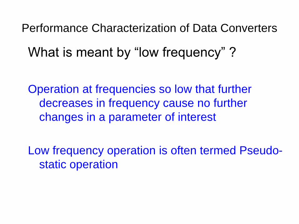
What is meant by “low frequency” ?
Operation at frequencies so low that further
decreases in frequency cause no further
changes in a parameter of interest
Low frequency operation is often termed Pseudo-
static operation
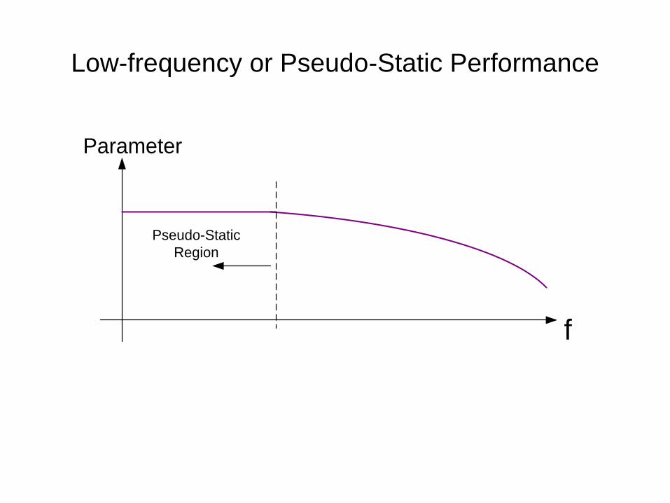
Low-frequency or Pseudo-Static Performance
f
Parameter
Pseudo-Static
Region
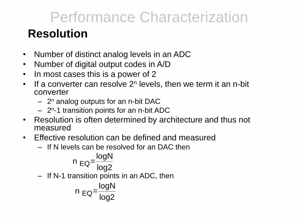
Performance Characterization
• Number of distinct analog levels in an ADC
• Number of digital output codes in A/D
• In most cases this is a power of 2
• If a converter can resolve 2n levels, then we term it an n-bit converter– 2n analog outputs for an n-bit DAC
– 2n-1 transition points for an n-bit ADC
• Resolution is often determined by architecture and thus not measured
• Effective resolution can be defined and measured– If N levels can be resolved for an DAC then
– If N-1 transition points in an ADC, then
Resolution
EQlogN
n =log2
EQlogN
n =log2
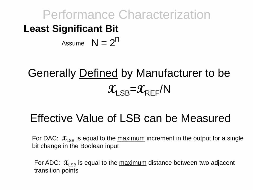
Performance Characterization
Generally Defined by Manufacturer to be
XLSB=XREF/N
Least Significant Bit
Assume nN = 2
Effective Value of LSB can be Measured
For DAC: XLSB is equal to the maximum increment in the output for a single
bit change in the Boolean input
For ADC: XLSB is equal to the maximum distance between two adjacent
transition points
Performance Characterization of Data Converters
• Static characteristics– Resolution
– Least Significant Bit (LSB)
– Offset and Gain Errors
– Absolute Accuracy
– Relative Accuracy
– Integral Nonlinearity (INL)
– Differential Nonlinearity (DNL)
– Monotonicity (DAC)
– Missing Codes (ADC)
– Quantization Noise
– Low-f Spurious Free Dynamic Range (SFDR)
– Low-f Total Harmonic Distortion (THD)
– Effective Number of Bits (ENOB)
– Power Dissipation
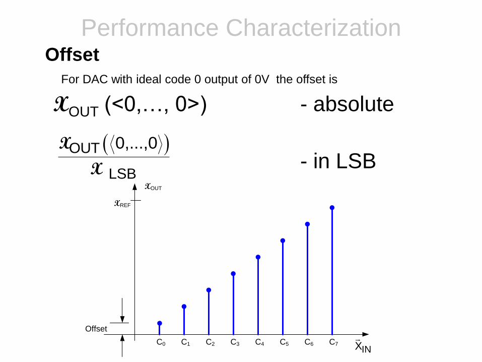
Performance Characterization
XOUT (<0,…, 0>) - absolute
- in LSB
Offset
For DAC with ideal code 0 output of 0V the offset is
OUT
LSB
0,...,0
X
XXOUT
INXC0 C1 C2 C3 C4 C5 C6 C7
XREF
Offset
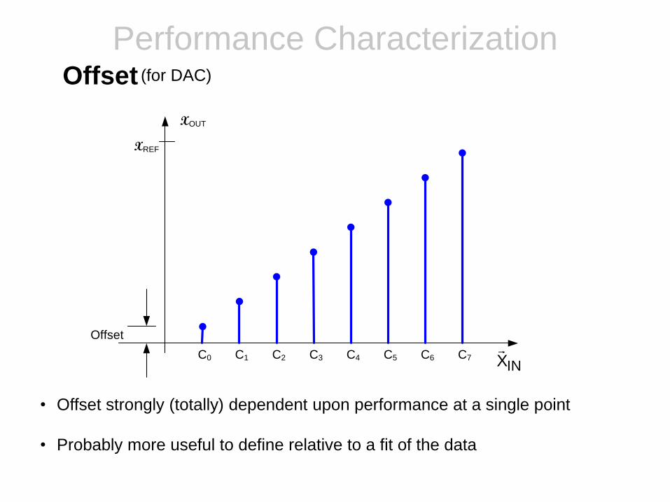
Performance CharacterizationOffset
XOUT
INXC0 C1 C2 C3 C4 C5 C6 C7
XREF
Offset
• Offset strongly (totally) dependent upon performance at a single point
• Probably more useful to define relative to a fit of the data
(for DAC)
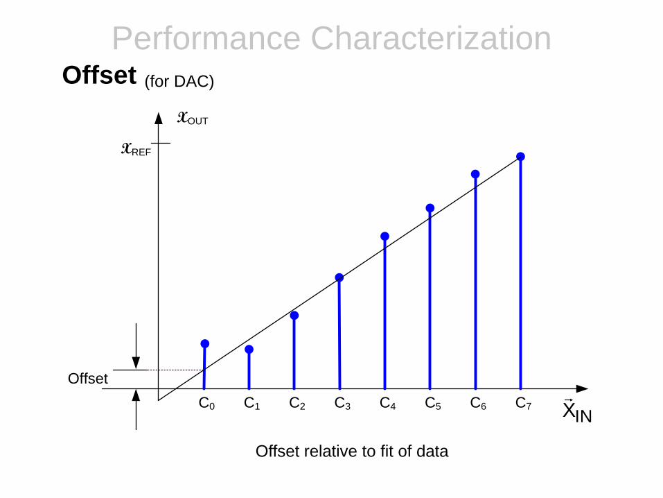
Performance CharacterizationOffset
Offset relative to fit of data
XOUT
INXC0 C1 C2 C3 C4 C5 C6 C7
XREF
Offset
(for DAC)
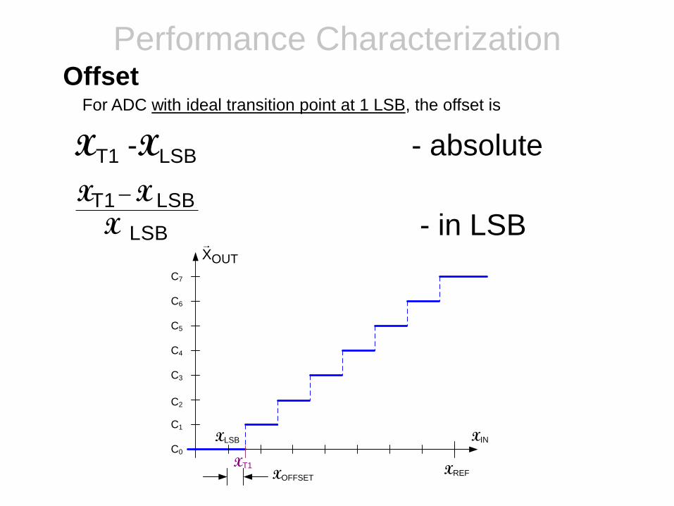
Performance Characterization
XT1 -XLSB - absolute
- in LSB
OffsetFor ADC with ideal transition point at 1 LSB, the offset is
T1 LSB
LSB
X X
X
XIN
OUTX
XREF
C0
C1
C2
C3
C4
C5
C6
C7
XLSB
XOFFSET
XT1
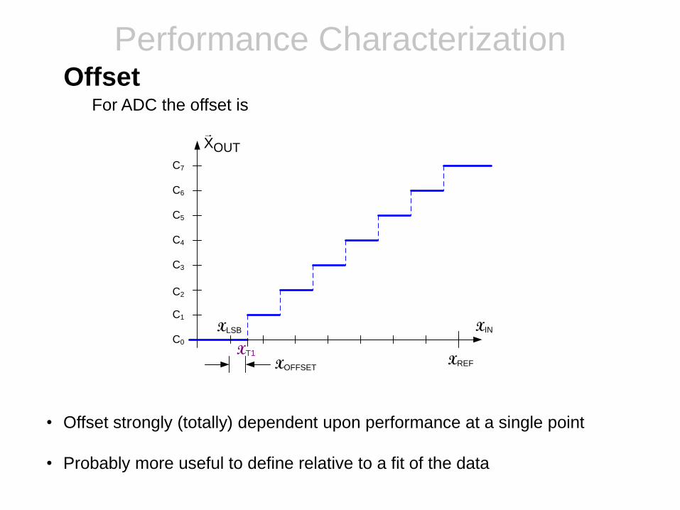
Performance CharacterizationOffset
For ADC the offset is
XIN
OUTX
XREF
C0
C1
C2
C3
C4
C5
C6
C7
XLSB
XOFFSET
XT1
• Offset strongly (totally) dependent upon performance at a single point
• Probably more useful to define relative to a fit of the data
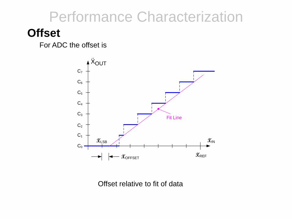
Performance CharacterizationOffset
For ADC the offset is
XIN
OUTX
XREF
C0
C1
C2
C3
C4
C5
C6
C7
XLSB
XOFFSET
Fit Line
Offset relative to fit of data
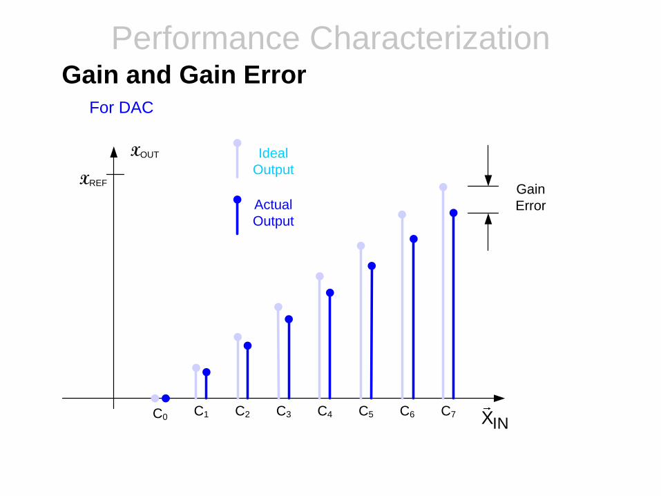
Performance CharacterizationGain and Gain Error
XOUT
INXC0C1 C2 C3 C4 C5 C6 C7
XREFGain
Error
Ideal
Output
Actual
Output
For DAC
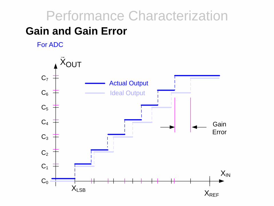
Performance CharacterizationGain and Gain Error
XIN
OUTX
XREF
C0
C1
C2
C3
C4
C5
C6
C7
XLSB
Gain
Error
Actual Output
Ideal Output
For ADC
Performance Characterization
Gain and Offset Errors
• Fit line would give better indicator of error in gain but less practical to
obtain in test
• Gain and Offset errors of little concern in many applications
• Performance of systems using data converters is often nearly
independent of gain and offset errors
• Can be trimmed in field if gain or offset errors exist and are of concern
Performance Characterization of Data Converters
• Static characteristics– Resolution
– Least Significant Bit (LSB)
– Offset and Gain Errors
– Absolute Accuracy
– Relative Accuracy
– Integral Nonlinearity (INL)
– Differential Nonlinearity (DNL)
– Monotonicity (DAC)
– Missing Codes (ADC)
– Quantization Noise
– Low-f Spurious Free Dynamic Range (SFDR)
– Low-f Total Harmonic Distortion (THD)
– Effective Number of Bits (ENOB)
– Power Dissipation
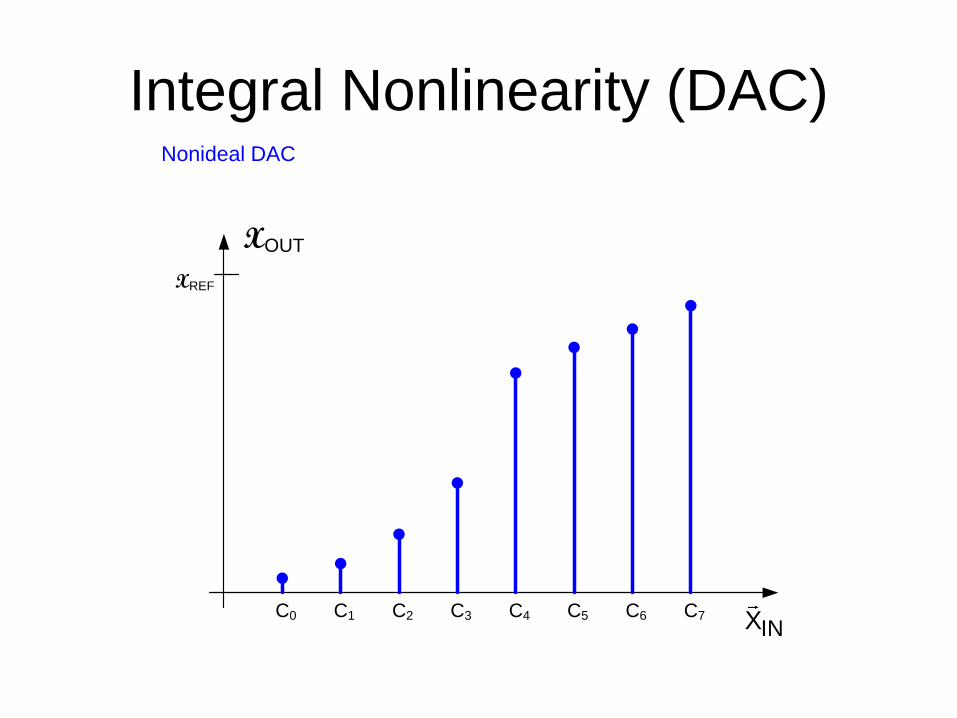
Integral Nonlinearity (DAC)
INXC0 C1 C2 C3 C4 C5 C6 C7
XREF
XOUT
Nonideal DAC
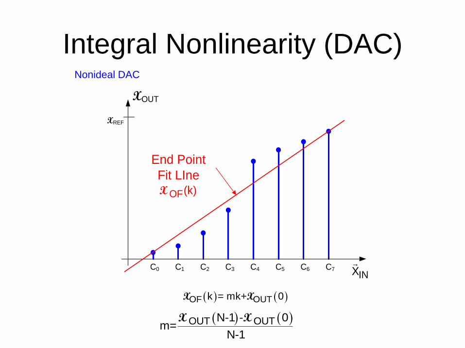
Integral Nonlinearity (DAC)Nonideal DAC
INXC0 C1 C2 C3 C4 C5 C6 C7
XREF
End Point
Fit LIne
XOUT
OF(k)X
OF OUTk = mk+ 0X X
OUT OUTN-1 - 0m=
N-1
X X
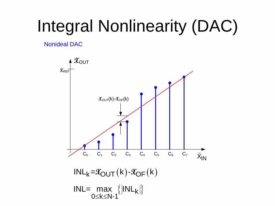
Integral Nonlinearity (DAC)Nonideal DAC
INXC0 C1 C2 C3 C4 C5 C6 C7
XREF
XOUT(k)-XOF(k)
XOUT
k OUT OFINL = k - kX X
k0 k N-1
INL= max INL
Integral Nonlinearity (DAC)Nonideal DAC
INXC0 C1 C2 C3 C4 C5 C6 C7
XREF
INL
XOUT
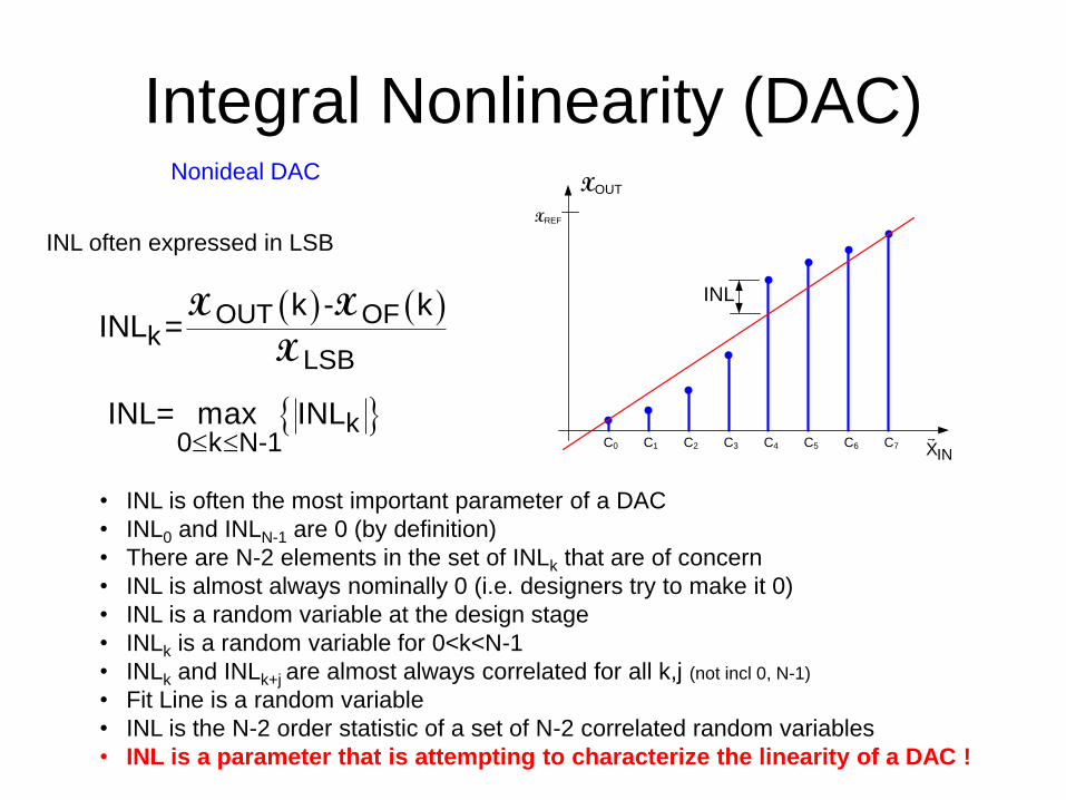
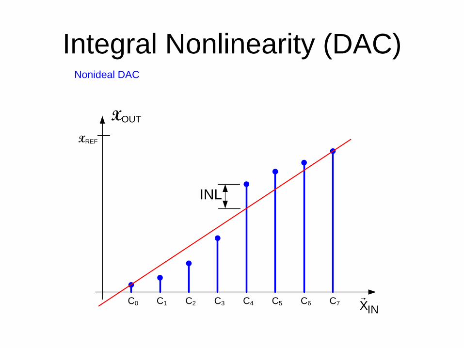
Integral Nonlinearity (DAC)Nonideal DAC
INXC0 C1 C2 C3 C4 C5 C6 C7
XREF
INL
XOUT
INL often expressed in LSB
OUT OFk
LSB
k - kINL =
X X
X
k0 k N-1
INL= max INL
• INL is often the most important parameter of a DAC
• INL0 and INLN-1 are 0 (by definition)
• There are N-2 elements in the set of INLk that are of concern
• INL is almost always nominally 0 (i.e. designers try to make it 0)
• INL is a random variable at the design stage
• INLk is a random variable for 0<k<N-1
• INLk and INLk+j are almost always correlated for all k,j (not incl 0, N-1)
• Fit Line is a random variable
• INL is the N-2 order statistic of a set of N-2 correlated random variables
• INL is a parameter that is attempting to characterize the linearity of a DAC !
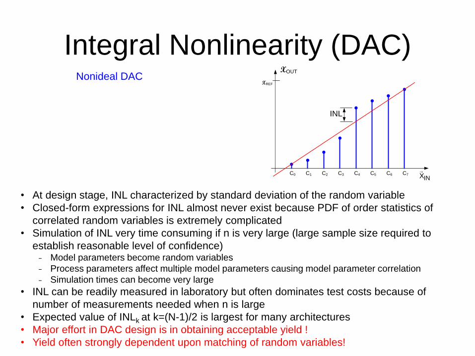
Integral Nonlinearity (DAC)Nonideal DAC
INXC0 C1 C2 C3 C4 C5 C6 C7
XREF
INL
XOUT
• At design stage, INL characterized by standard deviation of the random variable
• Closed-form expressions for INL almost never exist because PDF of order statistics of
correlated random variables is extremely complicated
• Simulation of INL very time consuming if n is very large (large sample size required to
establish reasonable level of confidence)− Model parameters become random variables
− Process parameters affect multiple model parameters causing model parameter correlation
− Simulation times can become very large
• INL can be readily measured in laboratory but often dominates test costs because of
number of measurements needed when n is large
• Expected value of INLk at k=(N-1)/2 is largest for many architectures
• Major effort in DAC design is in obtaining acceptable yield !
• Yield often strongly dependent upon matching of random variables!
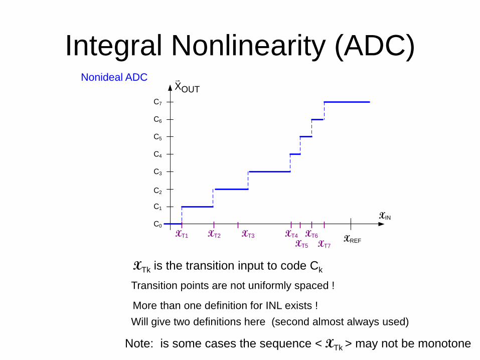
Integral Nonlinearity (ADC)Nonideal ADC
XIN
OUTX
XREF
C0
C1
C2
C3
C4
C5
C6
C7
XT1 XT2 XT3 XT4
XT5
XT6
XT7
Transition points are not uniformly spaced !
More than one definition for INL exists !
Will give two definitions here (second almost always used)
XTk is the transition input to code Ck
Note: is some cases the sequence < XTk > may not be monotone
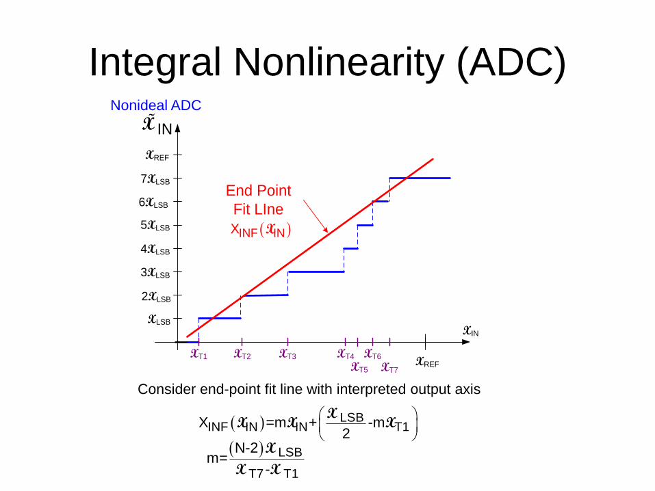
Integral Nonlinearity (ADC)Nonideal ADC
XIN
XREF
End Point
Fit LIne
XREF
XLSB
2XLSB
3XLSB
4XLSB
5XLSB
6XLSB
7XLSB
INX
XT1 XT2 XT3 XT4
XT5
XT6
XT7
INF INX X
Consider end-point fit line with interpreted output axis
LSBINF IN IN T1X =m + -m
2
XX X X
LSB
T7 T1
N-2m=
-
X
X X
Integral Nonlinearity (ADC)Nonideal ADC
XIN
XREF
End Point
Fit LIne
XREF
XLSB
2XLSB
3XLSB
4XLSB
5XLSB
6XLSB
7XLSB
INX
XT1 XT2 XT3 XT4
XT5
XT6
XT7
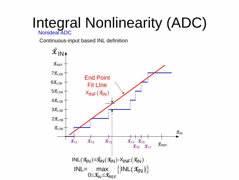
INF INX X
IN IN IN INF ININL = -XX X X X
IN REF
IN0
INL= max INL X X
X
Continuous-input based INL definition
Integral Nonlinearity (ADC)Nonideal ADC
XIN
XREF
End Point
Fit LIne
XREF
XLSB
2XLSB
3XLSB
4XLSB
5XLSB
6XLSB
7XLSB
INX
XT1 XT2 XT3 XT4
XT5
XT6
XT7
INF INX X
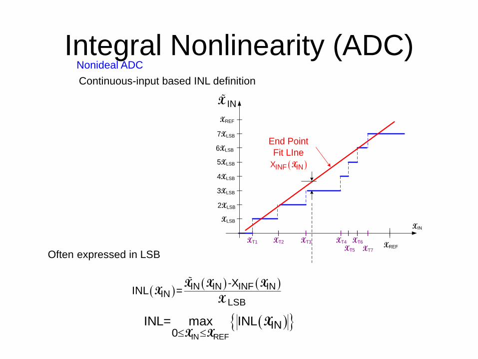
IN IN INF IN
IN LSB
-XINL =
X X XX
X
IN REF
IN0
INL= max INL X X
X
Continuous-input based INL definition
Often expressed in LSB
Integral Nonlinearity (ADC)Nonideal ADC
XIN
XREF
End Point
Fit LIne
XREF
XLSB
2XLSB
3XLSB
4XLSB
5XLSB
6XLSB
7XLSB
INX
XT1 XT2 XT3 XT4
XT5
XT6
XT7
INF INX X
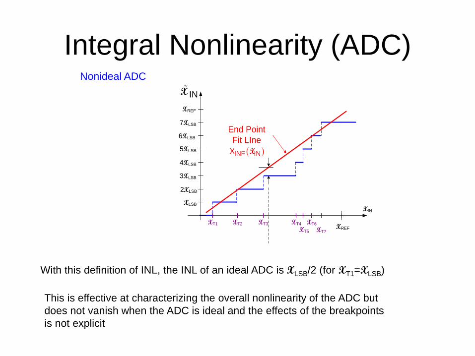
With this definition of INL, the INL of an ideal ADC is XLSB/2 (for XT1=XLSB)
This is effective at characterizing the overall nonlinearity of the ADC but
does not vanish when the ADC is ideal and the effects of the breakpoints
is not explicit
Integral Nonlinearity (ADC)Nonideal ADC
XIN
OUTX
XREF
C0
C1
C2
C3
C4
C5
C6
C7
XT1 XT2 XT3 XT4
XT5
XT6
XT7
XIN
XFT1 XFT2 XFT3 XFT4 XFT5 XFT6 XFT7
INL3
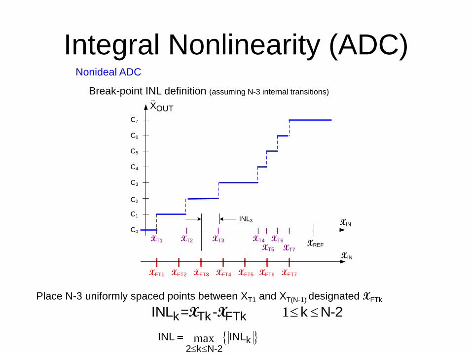
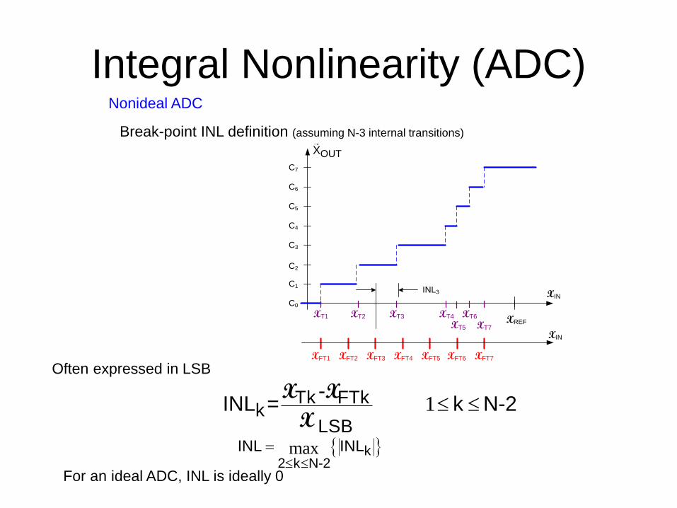
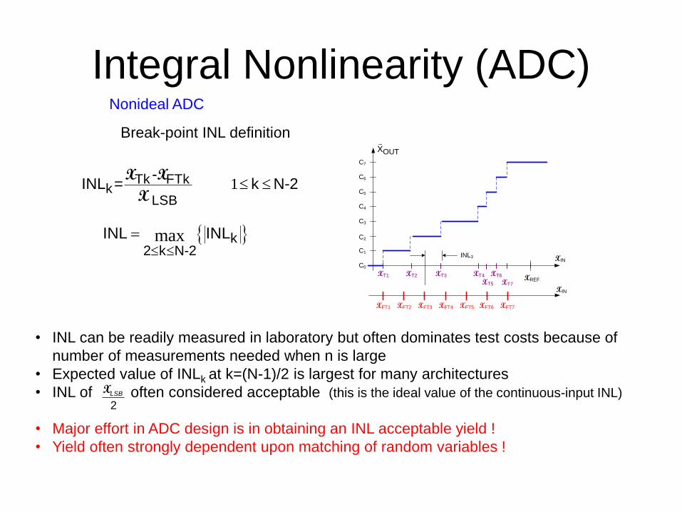
Break-point INL definition (assuming N-3 internal transitions)
Place N-3 uniformly spaced points between XT1 and XT(N-1) designated XFTk
max k2 k N-2
INL INL
1k Tk FTkINL = - k N-2 X X
Integral Nonlinearity (ADC)Nonideal ADC
XIN
OUTX
XREF
C0
C1
C2
C3
C4
C5
C6
C7
XT1 XT2 XT3 XT4
XT5
XT6
XT7
XIN
XFT1 XFT2 XFT3 XFT4 XFT5 XFT6 XFT7
INL3
Break-point INL definition (assuming N-3 internal transitions)
max k2 k N-2
INL INL
Often expressed in LSB
1Tk FTkk
LSB
-INL = k N-2
X X
X
For an ideal ADC, INL is ideally 0
Integral Nonlinearity (ADC)Nonideal ADC
XIN
OUTX
XREF
C0
C1
C2
C3
C4
C5
C6
C7
XT1 XT2 XT3 XT4
XT5
XT6
XT7
XIN
XFT1 XFT2 XFT3 XFT4 XFT5 XFT6 XFT7
INL3
Break-point INL definition (assuming N-3 internal transitions)
max k2 k N-2
INL INL
1Tk FTkk
LSB
-INL = k N-2
X X
X
• INL is often the most important parameter of an ADC
• INL1 and INLN-1 are 0 (by definition)
• There are N-3 elements in the set of INLk that are of concern
• INL is a random variable at the design stage
• INLk is a random variable for 0<k<N-1
• INLk and INLk+j are correlated for all k,j (not incl 0, N-1) for most architectures
• Fit Line (for cont INL) and uniformly spaced break pts (breakpoint INL) are random variables
• INL is the N-3 order statistic of a set of N-3 correlated random variables (breakpoint INL)
• INL is a parameter that is attempting to characterize the linearity of an ADC !
Integral Nonlinearity (ADC)Nonideal ADC
XIN
OUTX
XREF
C0
C1
C2
C3
C4
C5
C6
C7
XT1 XT2 XT3 XT4
XT5
XT6
XT7
XIN
XFT1 XFT2 XFT3 XFT4 XFT5 XFT6 XFT7
INL3
Break-point INL definition (assuming N-3 internal transitions)
max k2 k N-2
INL INL
1Tk FTlk
LSB
-INL = k N-2
X X
X
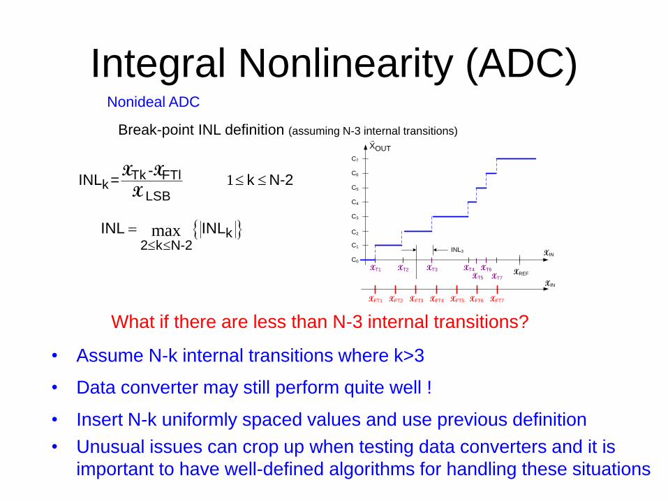
What if there are less than N-3 internal transitions?
• Assume N-k internal transitions where k>3
• Data converter may still perform quite well !
• Insert N-k uniformly spaced values and use previous definition
• Unusual issues can crop up when testing data converters and it is
important to have well-defined algorithms for handling these situations
Integral Nonlinearity (ADC)Nonideal ADC
XIN
OUTX
XREF
C0
C1
C2
C3
C4
C5
C6
C7
XT1 XT2 XT3 XT4
XT5
XT6
XT7
XIN
XFT1 XFT2 XFT3 XFT4 XFT5 XFT6 XFT7
INL3
Break-point INL definition
max k2 k N-2
INL INL
1Tk FTkk
LSB
-INL = k N-2
X X
X
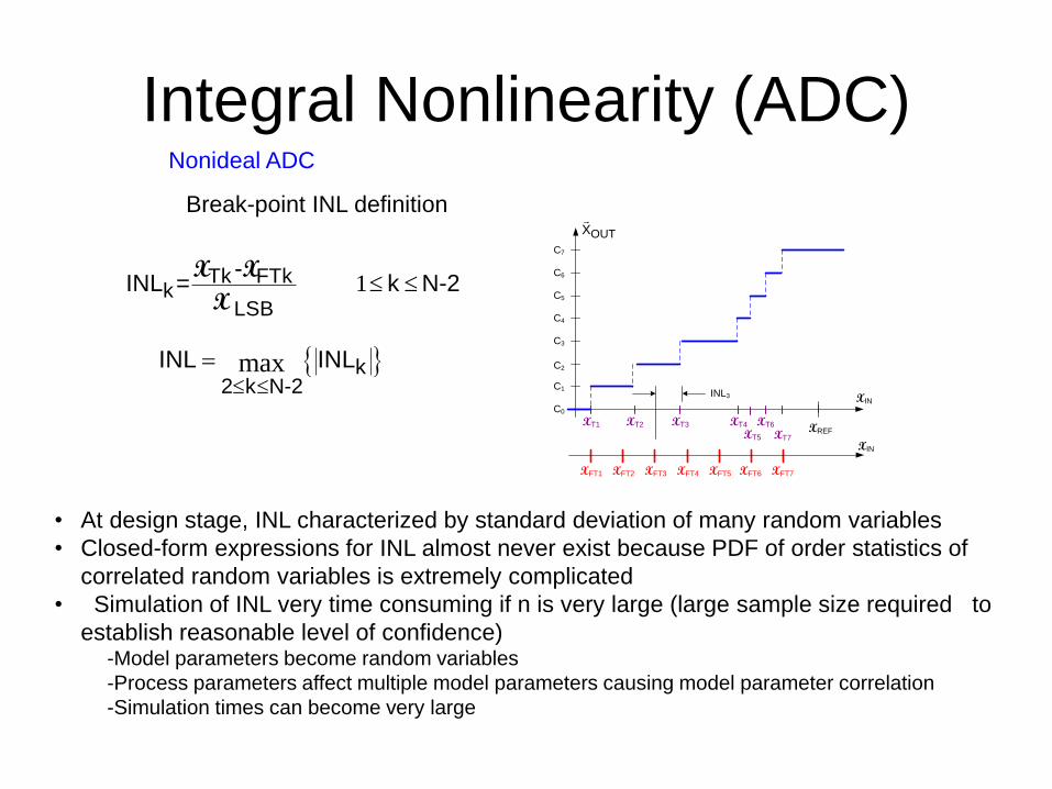
• At design stage, INL characterized by standard deviation of many random variables
• Closed-form expressions for INL almost never exist because PDF of order statistics of
correlated random variables is extremely complicated
• Simulation of INL very time consuming if n is very large (large sample size required to
establish reasonable level of confidence)-Model parameters become random variables
-Process parameters affect multiple model parameters causing model parameter correlation
-Simulation times can become very large
Integral Nonlinearity (ADC)Nonideal ADC
XIN
OUTX
XREF
C0
C1
C2
C3
C4
C5
C6
C7
XT1 XT2 XT3 XT4
XT5
XT6
XT7
XIN
XFT1 XFT2 XFT3 XFT4 XFT5 XFT6 XFT7
INL3
Break-point INL definition
max k2 k N-2
INL INL
1Tk FTkk
LSB
-INL = k N-2
X X
X
• INL can be readily measured in laboratory but often dominates test costs because of
number of measurements needed when n is large
• Expected value of INLk at k=(N-1)/2 is largest for many architectures
• INL of often considered acceptable (this is the ideal value of the continuous-input INL)
• Major effort in ADC design is in obtaining an INL acceptable yield !
• Yield often strongly dependent upon matching of random variables !
2LSBX

Stay Safe and Stay Healthy !

End of Lecture 1


![Behavior of Faulty Double BJT BiCMOS Logic Gates' · PDF file8.4.2 out the testability differences between the three logic families, namely; TTL, CMOS and BiCMOS. Levitt et. al. [9]](https://static.documents.pub/doc/80x56/5aa492f97f8b9afa758c1869/behavior-of-faulty-double-bjt-bicmos-logic-gates-out-the-testability-differences.jpg)


