EE4800 CMOS Digital IC Design & Analysis Lecture 9 Combinational Circuit Design Zhuo Feng Z. Feng MTU EE4800 CMOS Digital IC Design & Analysis 2010 Z. Feng MTU EE4800 CMOS Digital IC Design & Analysis 2010 9. 9.1
Transcript
EE4800 CMOS Digital IC Design & Analysis
Lecture 9 Combinational Circuit DesignZhuo Feng
Z. Feng MTU EE4800 CMOS Digital IC Design & Analysis 2010Z. Feng MTU EE4800 CMOS Digital IC Design & Analysis 20109.9.11
Outline■ Bubble Pushing■ Compound Gatesp■ Logical Effort Example■ Input Orderingp g■ Asymmetric Gates■ Skewed Gates■ Skewed Gates■ Best P/N ratio
Z. Feng MTU EE4800 CMOS Digital IC Design & Analysis 2010Z. Feng MTU EE4800 CMOS Digital IC Design & Analysis 20109.9.22
Example 11) Sketch a design using NAND, NOR, and NOT gates.
Assume ~S is available.
Y
D0S
YD1S
Z. Feng MTU EE4800 CMOS Digital IC Design & Analysis 2010Z. Feng MTU EE4800 CMOS Digital IC Design & Analysis 20109.9.33
Bubble Pushingg■ Start with network of AND / OR gates■ Convert to NAND / NOR + inverters■ Push bubbles around to simplify logic
► Remember DeMorgan’s Law
Y YY Y
(a) (b)
Y
D
Y
(c) (d)
Z. Feng MTU EE4800 CMOS Digital IC Design & Analysis 2010Z. Feng MTU EE4800 CMOS Digital IC Design & Analysis 20109.9.44
( ) ( )
Example 22) Sketch a design using one compound gate and
one NOT gate. Assume ~S is available.g
D0S YSD1SS
Z. Feng MTU EE4800 CMOS Digital IC Design & Analysis 2010Z. Feng MTU EE4800 CMOS Digital IC Design & Analysis 20109.9.55
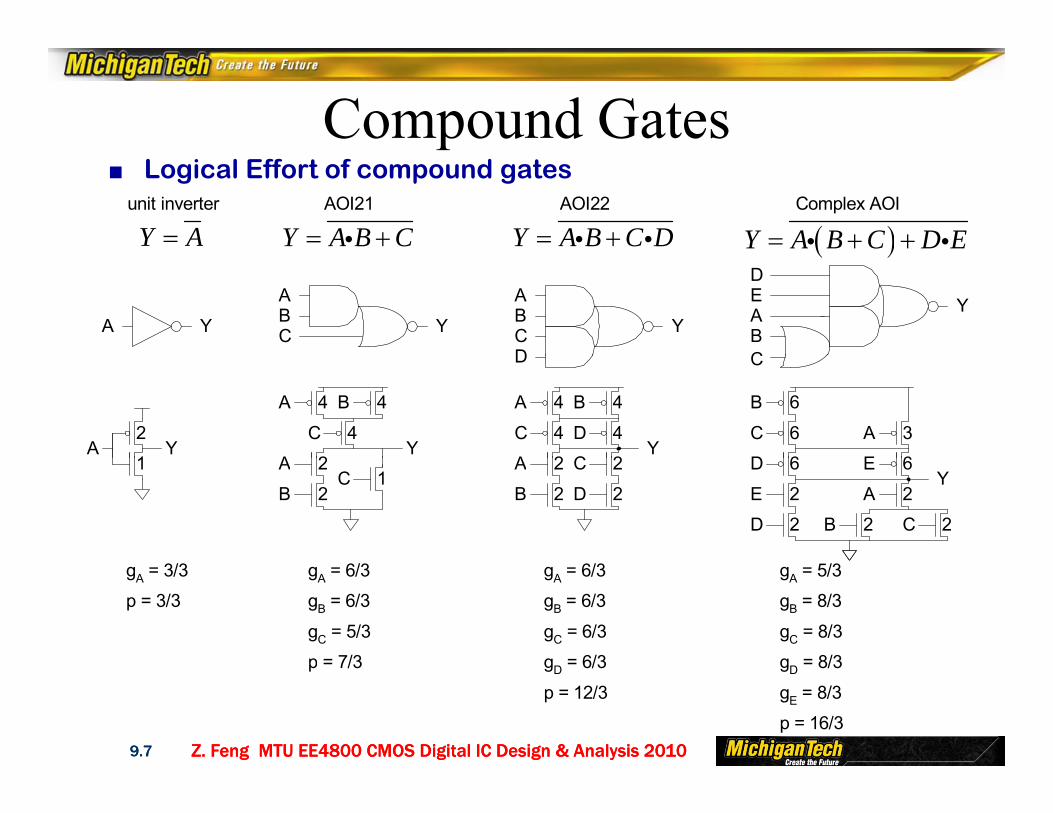
Compound Gates■ Logical Effort of compound gates
unit inverter AOI21 AOI22 Complex AOI
Y A B C= +i Y A B C D= +i i ( )Y A B C D E= + +i iY A=
ABCD
Y
ABC YYA A
C
DE Y
B
( )
D
AC
C
A B
A C
A
C
B
D
21
4
44
2 2
4
4 4
4A Y
2
1YY
C
Y
A
B
C
D E
6
6
6 6
3
BC
B D21
2 2
gA = 6/3 gA =gA = 3/3
Y
B C
A
D
E
gA =
2
2 2
22
gB = 6/3
gC = 5/3
p = 7/3
gB =
gC =
p =
gD =
p = 3/3 gB =
gC =
gD =
g =
Z. Feng MTU EE4800 CMOS Digital IC Design & Analysis 2010Z. Feng MTU EE4800 CMOS Digital IC Design & Analysis 20109.9.66
p =
p =
gE =
Compound Gates■ Logical Effort of compound gates
unit inverter AOI21 AOI22 Complex AOI
Y A B C= +i Y A B C D= +i i ( )Y A B C D E= + +i iY A=
ABCD
Y
ABC YYA A
C
DE Y
B
( )
D
A
C
A B
A C
A
C
B
D
2
4
44
2 2
4
4 4
4A Y
2
1YY
C
A
B
C
D E
6
6
6 6
3
A
BC
A
B
C
D2
21
2
2 2
2
1Y
B C
A
D
E
D E
2
2 2
22
6 6
gA = 6/3
gB = 6/3
gC = 5/3
p = 7/3
gA = 6/3
gB = 6/3
gC = 6/3
g = 6/3
gA = 3/3
p = 3/3
gA = 5/3
gB = 8/3
gC = 8/3
g = 8/3
Z. Feng MTU EE4800 CMOS Digital IC Design & Analysis 2010Z. Feng MTU EE4800 CMOS Digital IC Design & Analysis 20109.9.77
p = 7/3
p = 12/3
gD = 6/3 gD = 8/3
p = 16/3
gE = 8/3
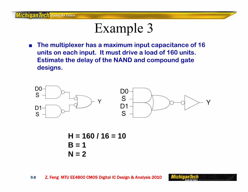
Example 3■ The multiplexer has a maximum input capacitance of 16
units on each input. It must drive a load of 160 units. Estimate the delay of the NAND and compound gate Estimate the delay of the NAND and compound gate designs.
Y
D0S
D1Y
D0SD1D1
SD1S
H = 160 / 16 = 10B = 1N = 2
Z. Feng MTU EE4800 CMOS Digital IC Design & Analysis 2010Z. Feng MTU EE4800 CMOS Digital IC Design & Analysis 20109.9.88
NAND Solution
D02 2 4P = + =
Y
D0S
D1S
(4 / 3) (4 / 3) 16 / 9160 / 9
GF GBH= =i
S160 / 9ˆ 4.2N
F GBH
f F
= =
= =ˆ 12.4D Nf P τ= + =
Z. Feng MTU EE4800 CMOS Digital IC Design & Analysis 2010Z. Feng MTU EE4800 CMOS Digital IC Design & Analysis 20109.9.99
Compound Solution
4 1 5P = + = D05(6 / 3) (1) 2
20GF GBH= =i Y
D0SD1S20
ˆ 4.5N
F GBH
f F
= =
= =
S
ˆ 14D Nf P τ= + =
Z. Feng MTU EE4800 CMOS Digital IC Design & Analysis 2010Z. Feng MTU EE4800 CMOS Digital IC Design & Analysis 20109.9.1010
Example 4■ Annotate your designs with transistor
sizes that achieve this delay.y
88
6 6
10
10Y
24
12
10
10
8
8
25
2525Y
6
6 6
6
12
8
8825
25
816 16160 * (4/3) / 4.2 = 50 160 * 1 / 4.5 = 36
Z. Feng MTU EE4800 CMOS Digital IC Design & Analysis 2010Z. Feng MTU EE4800 CMOS Digital IC Design & Analysis 20109.9.1111
Input Order■ Our parasitic delay model was too simple
► Calculate parasitic delay for Y falling▼ If A arrives latest? 2τ▼ If B arrives latest? 2.33τ
22 Y6C
2C2
2
B
Ax
Y
2C2B x
Z. Feng MTU EE4800 CMOS Digital IC Design & Analysis 2010Z. Feng MTU EE4800 CMOS Digital IC Design & Analysis 20109.9.1212
Inner & Outer Inputs■ Outer input is closest to rail (B)■ Inner input is closest to output (A) 22■ Inner input is closest to output (A)
■ If input arrival time is known2
2
22
B
A
Y
► Connect latest input to inner terminal 2B
Z. Feng MTU EE4800 CMOS Digital IC Design & Analysis 2010Z. Feng MTU EE4800 CMOS Digital IC Design & Analysis 20109.9.1313
Asymmetric Gatesy■ Asymmetric gates favor one input over another■ Ex: suppose input A of a NAND gate is most critical
► Use smaller transistor on A (less capacitance)► Use smaller transistor on A (less capacitance)► Boost size of noncritical input► So total resistance is same
A Yreset
Y
■ gA = 10/9 2 4
4/3
22
reset
AY
■ gB = 2■ gtotal = gA + gB = 28/9■ Asymmetric gate approaches g = 1 on critical input
4reset
Z. Feng MTU EE4800 CMOS Digital IC Design & Analysis 2010Z. Feng MTU EE4800 CMOS Digital IC Design & Analysis 20109.9.1414
■ But total logical effort goes up
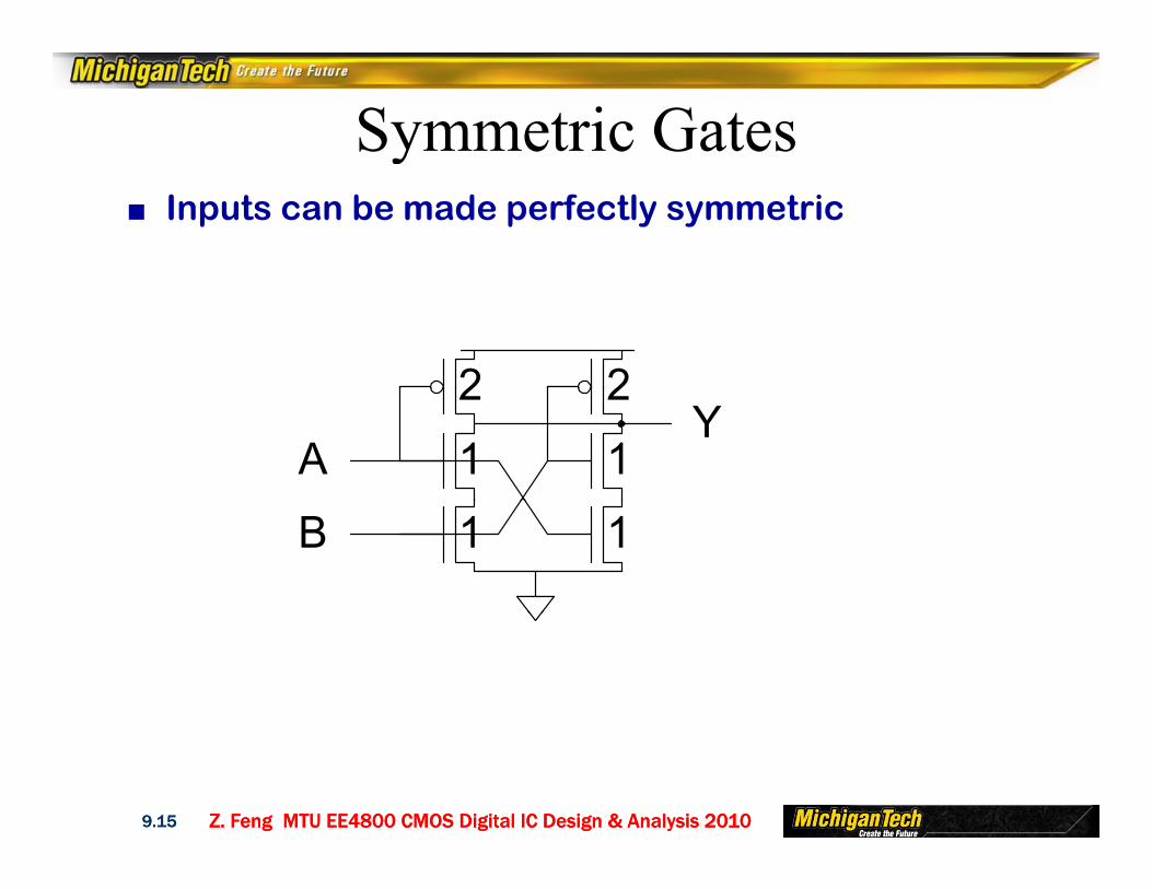
Symmetric Gatesy■ Inputs can be made perfectly symmetric
2 2
AY
2
1
2
1
B 1 1
Z. Feng MTU EE4800 CMOS Digital IC Design & Analysis 2010Z. Feng MTU EE4800 CMOS Digital IC Design & Analysis 20109.9.1515
Skewed Gates■ Skewed gates favor one edge over another■ Ex: suppose rising output of inverter is most critical
D i iti l MOS t i t► Downsize noncritical nMOS transistor
HI-skewinverter
unskewed inverter(equal rise resistance)
unskewed inverter(equal fall resistance)
1/2
2A Y
1
2A Y
1/2
1A Y
( q ) ( q )
■ Calculate logical effort by comparing to unskewed inverter ■ Calculate logical effort by comparing to unskewed inverter with same effective resistance on that edge.► gu = 2.5 / 3 = 5/6► g = 2 5 / 1 5 = 5/3
Z. Feng MTU EE4800 CMOS Digital IC Design & Analysis 2010Z. Feng MTU EE4800 CMOS Digital IC Design & Analysis 20109.9.1616
► gd = 2.5 / 1.5 = 5/3
HI- and LO-Skew■ Def: Logical effort of a skewed gate for a particular
transition is the ratio of the input capacitance of that gate to the input capacitance of an unskewed inverter to the input capacitance of an unskewed inverter delivering the same output current for the same transition.