12
나노정보과학기술원 광원-디스플레이학과 정보·나노공학과

나노정보과학기술원광원-디스플레이학과
정보·나노공학과

540
광원-디스플레이학과Department of Intelligent Light and Display
2 0 1 4 대 학 원 요 람
교육목표나노정보과학기술원 (NITA : Nano Information Technology Academy)의 산하 교육기관인 대학원의 광원-디스플레이 학과는 본교 및 NITA의 교육목적을 바탕으로 차세대 나노기술을 신기능 정보 및 디스플레이 분야에 응용하기 위한 융합 학문 및 기술 분야의 전문 인재를 양성하는 것을 목적으로 한다. 정보시스템의 급속한 발전으로 인한 고급 인력수요의 급증에 대처하기 위해 교육과 연구를 동시에 수행하여, 기초지식을 체계적으로 확립하고, 창의적인 능력과 문제해결력을 겸비한 나노융합 분야 및 정보-디스플레이 분야의 기초와 실무를 겸비한 전문인의 양성을 목표로 한다.
l NT 기초지식과 IT 응용지식을 겸비한 전문인 양성l 산업체 중심의 실무 특화 교육
l 국제화된 교육 및 연구 시스템을 활용한 경쟁력 있는 고급인력 양성
진로 및 취업분야- 장비관련 엔지니어- 전문대학원 진학- 대학원 진학 후 기업연구소 및 국책연구소의 연구 원- 기술직 공무원 및 기타
과정별 개설전공■ 석사학위과정 : 고체발광소자■ 박사학위과정 : 고체발광소자
대학원 선수과목 및 종합시험■ 선수과목 : 해당 없음
■ 종합시험의 응시자격석사학위과정 * 3학기이상 정규등록을 필한 자* 학점을 18학점이상 이수하고 그 평균성적이 B0(80점)이상인 자* 지도교수 및 주임교수의 추천을 받은 자
박사학위과정 * 4학기이상 정규등록을 필한 자 * 학점을 27학점이상 이수하고 그 평균성적이 B0(80점)이상인 자 * 지도교수 및 주임교수의 추천을 받은 자

541
14
■ 종합시험과목표과정 전공별 시험과목 (통과기준) 고체발광소자전공
석사공통 (1) 조명공학을 위한 반도체 물리학 I전공 (1) 조명공학을 위한 반도체광전소자
종합시험면제 재학 중 국제저명A 학술지에 주저자로 논문1편 게재시 종합시험 합격으로 인정
박사
공통 (1) 나노과학을 위한 고체물리학 특론전공 (2) 정보공학을 위한 정보디스플레이 I나노과학을 위한 반도체소자 물리학
종합시험면제 재학 중 국제저명A 학술지에 주저자로 논문2편 게재를 원칙다만, 논문게재가 어려운 학생은 지도교수및 주임교수의 승인을 통해 종합시험 응시 및 합격 인정
■ 졸업요건 (학칙에 기재된 사항) 석사학위과정 전공24학점 이수, 종합시험/영어시험 통과, 초록발표, 논문심사박사학위과정 전공36학점 이수, 종합시험/영어시험 통과, 연구실적 기준 충족, 초록발표, 논문심사
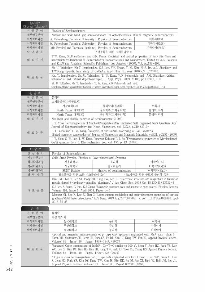
교수소개강 태 원
전 공 분 야 고체물리학세부연구분야 반도체물리학학사학위과정 동국대학(교) 물리학과(전공) 이학사석사학위과정 동국대학(교) 물리학과(전공) 이학 석사박사학위과정 동국대학(교) 물리학과(전공) 이학 박사담 당 과 목 조명공학을위한고체물리학1 고체물리학특론1
대 표 논 문
Sejoon Lee, Yoon Shon, Deuk Young Kim, Tae Won Kang, and Chong S. Yoon, "Enhanced ferromagnetism in H2O2-treated p-(Zn0.93Mn0.07)O layer" Appl. Phys. Lett.96(4),042115(2010.01.25)Yoon Shon, Sejoon Lee, D. Y. Kim, T. W. Kang, Chong S. Yoon, Eun Kyu Kim, and Jeong Ju Lee, "The structural, optical, magnetic properties, and anomalous Hall effect of InMnP:Zn epilayer" New J. Phys. 10, 115002(2008.11.14)Yoon Shon, Sejoon Lee, Tae Won Kang, Youngmin Lee, Seung-Woong Lee, Jin Dong Song, Hyung-Jun Kim, Jeong Ju Lee, Im Taek Yoon, Enlarged ferromagnetic hysteresis in InMnP:Be epilayers formed by thermal diffusion using MBE-grown Mn/InP:Be bilayers" J. Cryst. Growth 312(14), 2069-2072(2010.07.01)
파닌 (Gennady Panin)
전 공 분 야 Physics of semiconductors세부연구분야 Graphene학사학위과정 Moscow University Applied Physics and Electronics 이학사(BS)석사학위과정 Moscow University Applied Physics and Electronics 이학석사(MS)박사학위과정 IMT R.A.S Physics of semiconductors 이학박사(PhD)담 당 과 목 조명공학을위한 광학특론1 조명공학을위한 광학특론2
대 표 논 문
G. N. Panin, O.O. Kapitanova, S. W. Lee, A.N. Baranov and T.W. Kang"RESISTIVE SWITCHING IN Al/GRAPHENE OXIDE/Al STRUCTURE"Extended Abstracts In book 2nd,Int. Symposium on Graphene Devices: Technology,Physics and Modeling V 1, p. 94-95(201009.29) S. S. Kurbanov, G. N. Panin, T. W. Kim, T. W. Kang "Strong violet luminescence from ZnO nanocrystals grown by the low temperature chemical solution deposition"J. Luminescence 129,1099(2009)S. S. Kurbanov, G. N. Panin, and T. W. Kang "Spatially-resolved investigations of the emission around 3.31 eV (A-line) from ZnO nanocrystals" Appl. Phys. Letters 95, 211902(2009)
542
율다세프 (Shavkat Yuldashev)전 공 분 야 Physics of Semiconductors세부연구분야 Narrow and wide band-gap semiconductors for optoelectronics, Diluted magnetic semiconductors학사학위과정 St. Petersburg Technical University Physics of Semiconductors 이학사(BS)석사학위과정 St. Petersburg Technical University Physics of Semiconductors 이학석사(MS)박사학위과정 Ioffe Physical and Technical Institute Physics of Semiconductors 이학박사(Ph.D)담 당 과 목 조명공학을 위한 고체물리학 2대 표 저 서 T.W. Kang, Sh.U.Yuldashev and G.N. Panin, Electrical and optical properties of ZnO thin films and nanostructures.Handbook of Semiconductor Nanostructures and Nanodevices, Edited by A.A. Balandin and K.L.Wang, American Scientific Publishers, Los Angeles (2006), V.4, pp.159-194.
대 표 논 문
Sh. U. Yuldashev, Kh.T. Igamberdiev, S.J. Lee, Y.H. Kwon, Y. M. Kim, H. S. Im, A.G, Shashkov, and T.W.Kang, Specific heat study of GaMnAs, Appl. Phys. Express 2010,V.3, p.073005.Kh. T. Igamberdiev, Sh. U. Yuldashev, T. W. Kang, V.O. Pelenovich, and A.G. Shashkov, Critical behavior of Zn1-xMnxOdopedbynitrogen, J. Appl. Phys., 2009, V.105, pp.113920_1-3.Sh. U. Yuldashev, Kh. T. Igamberdiev, T. W. Kang, V.O. Pelenovich, and A.G. Shashkov,MagneticphasetransitioninZn1-xMnxOdopedbynitrogen.Appl.Phys.Lett.,2008,V.93,pp.092503_1-3.
윤 임 택전 공 분 야 물리학세부연구분야 고체물리학(자성반도체)학사학위과정 서강대학(교) 물리학과(물리학) 이학사석사학위과정 North Texas 대학(교) 물리학과(고체물리학) 물리학 석사박사학위과정 North Texas 대학(교) 물리학과(고체물리학) 물리학 박사대 표 저 서 Nonlinear and chaotic behavior of semiconductor (1995)
대 표 논 문
I. T. Yoon “Ferromagnetism of Mn5Ge3PrecipitatesinMn-implanted Self-organized Ge/Si Quantum Dots” Journal of Superconductivity and Novel Magnetism, vol. 23(3), p.319 (2010)I. T. Yoon and T. W. Kang, “Analysis of the Raman scattering of Ga1-xMnxAsdiluted magnetic semiconductor” Journal of Magnetism and Magnetic Materials, vol321, p.2257 (2009)I. T. Yoon, S. W. Lee, T. W. Kang, Dongwan Koh and D. J. Fu, “Ferromagnetic properties of Mn-implanted Ge/Si quantum dots” J. Electrochemical Soc. vol. 155, p. K1 (2008).
이 승 주전 공 분 야 Physics of Semiconductors세부연구분야 Solid State Physics, Physics of Low-dimensional Systems학사학위과정 서울대학교 물리학 이학사(BS)석사학위과정 서울대학교 반도체물리 이학석사(MS)박사학위과정 SUNY Buffalo Physics of semiconductors 이학박사(Ph.D)담 당 과 목 정보공학을 위한 고급 디스플레이 소자 나노과학을 위한 반도체 물리학 특론
대 표 논 문
Baik JM, Shon Y, Lee SJ, Jeong YH, Kang TW, Lee JL. "Electronic structure and magnetism in transition metals doped 8-hydroxy-quinoline aluminum." J Am Chem Soc. 2008 Oct 15;130(41):13522-3S.J Lee, S Soum, G Ihm, K.J Chang "Magnetic quantum dots and magnetic edge states" Physics Reports, Volume 394, Issue 1, April 2004, Pages 1–40Myoung N1, Seo K, Lee SJ, Ihm G. "Large current modulation and spin-dependent tunneling of vertical graphene/MoS2 heterostructures." ACS Nano. 2013 Aug 27;7(8):7021-7. doi: 10.1021/nn402919d. Epub 2013 Jul 25
손 윤 전 공 분 야 물리학세부연구분야 자성 반도체학사학위과정 동국대학교 물리학 이학사석사학위과정 부산대학교 물리학 이학석사박사학위과정 동국대학교 물리학 이학박사
대 표 논 문
“Optical and magnetic measurements of p-type GaN epilayers implanted with Mn+ ions”, Shon Y, Kwon YH, Yuldashev SU, Leem JH, Park CS, Fu DJ, Kim HJ, Kang TW, Fan XJ, Applied Physics Letters, Volume: 81 Issue: 10 Pages: 1845-1847, (2002)"Enhanced Curie temperature of InMnP : Zn-T-C similar to 300 k", Shon Y, Jeon HC, Park YS, Lee WC, Lee SJ, Kim DY, Kim HS, Kim HJ, Kang TW, Park YJ, Yoon CS, Chung KS, Applied Physics Letters, Volume: 85 Issue: 10 Pages: 1736-1738 (2004)"Origin of clear ferromagnetism for p-type GaN implanted with Fe+ (5 and 10 at. %)", Shon Y, Lee S, Jeon HC, Park YS, Kim DY, Kang TW, Kim JS, Kim EK, Fu DJ, Fan XJ, Park YJ, Baik JM, Lee JL, Applied Physics Letters, Volume: 89 Issue: 8 Pages: 082505 (2006)

543
14
학수번호 교과목명 학점 이론 실습 이수대상 원어강의 비고ILD 6001 조명공학을 위한 반도체 물리학 I 3 3 석사 영어ILD 6002 조명공학을 위한 반도체 물리학 II 3 3 석사 영어ILD 6003 조명공학을 위한 고체물리학 I 3 3 석사 영어ILD 6004 조명공학을 위한 고체물리학 II 3 3 석사 영어ILD 6005 조명공학을 위한 성장학 3 3 석사 영어ILD 6006 조명공학을 위한 전자기학 3 3 석사 영어ILD 6007 조명공학을 위한 광학 특론 I 3 3 석사 영어ILD 6008 조명공학을 위한 광학 특론 II 3 3 석사 영어ILD 6012 나노과학을 위한 반도체소자 3 3 석사 영어ILD 6013 나노과학을 위한 반도체 물성 특론 3 3 석사 영어ILD 6015 나노과학을 위한 반도체 양자구조 특론 3 3 석사 영어ILD 6016 나노과학을 위한 양자역학 3 3 석사 영어ILD 6017 나노과학을 위한 양자반도체 구조론 3 3 석사 영어ILD 6018 조명공학을 위한 반도체광전소자 3 3 석사 영어ILD 6019 조명공학을 위한 광전자공학 3 3 석사 영어ILD 6021 나노과학을 위한 반도체 물리학 특론 3 3 석사 영어ILD 6023 조명공학을 위한 반도체소자 특론 3 3 석사 영어ILD 6024 나노과학을 위한 반도체 소자 물리학 세미나 3 3 석사 영어ILD 6025 나노과학을 위한 고체물리학 특론 3 3 석사 영어ILD 6027 나노과학을 위한 나노소자세미나 3 3 석사 영어ILD 8001 조명공학을 위한 광소자 제조 공정 3 3 박사 영어ILD 8003 조명공학을 위한 화합물 반도체 특론 3 3 박사 영어
전 희 창전 공 분 야 고체물리학세부연구분야 나노 반도체 물성 및 소자 연구학사학위과정 동국대학교 물리학과 이학사석사학위과정 동국대학교 고체물리학 전공 이학석사박사학위과정 동국대학교 고체물리학 전공 이학박사
대 표 논 문
"Electronic and optical properties of CdZnO quantum well structures with electric field and polarization effects", Applied Physics Letters 96, 101113 (2010) "Atomic arrangements of (Ga1-xMnx)N nanorods grown on Al2O3 substrates", Applied Physics Letters 92, 141919 (2008)“Dependence of the magnetic properties on the Mn/In flux ratio in self-assembled (In1-xMnx)As quantum dots", Journal of Crystal Growth, 310, 541-544 (2008)
가나파티 (Nagarajan Ganapathi Subramaniam)
전 공 분 야 Physics of Semiconductors세 부 연 구 분 야 ZnO, LED, FED, Non volatile memories, Topological insulators, Multiferrroic devices학 사 학 위 과 정 MadrasUniversity Physics 이학사(B.Sc)석 사 학 위 과 정 Bharathiar University Physics 이학석사(M.SC)박 사 학 위 과 정 Bharathiar –IITB-BARC Physics(SolidStatePhysics) 이학박사(Ph.D)담 당 과 목 조명공학을 위한 전자기학
대 표 논 문
JCLEE, N.G.Subramaniam, JW.lEE, Twkang "Study of ferroelectric and reproducible bistable switching properties in CdMnS thin films for nonvolatile memory applications" Applied Physics Letter 90(26),2007N.G.subramaniam, T.W.kang, Sspandia "Effect of halide ion concentration and irradiation dose dependent photostimulated luminescence investigation in the image screen phosphor CsBr1-xClx:Euy2" applied Physics B:Laser and Optics80(7),935-938(2004)Senthil, JCLEE, N.G.Subramaniam, JW.lEE, Twkang "Adsorption of Organophosphorous Pesticide from Aqueous Solution Using “Waste” Jute Fiber CarbonModern applied science 4(6), 2010
교과과정표
544
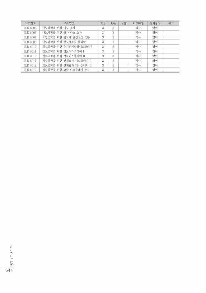
학수번호 교과목명 학점 이론 실습 이수대상 원어강의 비고ILD 8005 나노과학을 위한 나노 소자 3 3 박사 영어ILD 8006 나노과학을 위한 양자 나노 소자 3 3 박사 영어ILD 8007 조명공학을 위한 반도체 결정성장 특론 3 3 박사 영어ILD 8008 나노과학을 위한 반도체소자 물리학 3 3 박사 영어ILD 8010 정보공학을 위한 유기전기발광디스플레이 3 3 박사 영어ILD 8011 정보공학을 위한 정보디스플레이 I 3 3 박사 영어ILD 8012 정보공학을 위한 정보디스플레이 II 3 3 박사 영어ILD 8017 정보공학을 위한 전계효과 디스플레이 I 3 3 박사 영어ILD 8018 정보공학을 위한 전계효과 디스플레이 II 3 3 박사 영어ILD 8019 정보공학을 위한 고급 디스플레이 소자 3 3 박사 영어

545
14
정보·나노공학과Department of Information and Nanotechnology
2 0 1 4 대 학 원 요 람
교육목표나노정보과학기술원(NITA : Nano Information Technology Academy )의 산하 교육기관인 대학원의 정보·나노공학과는 본교 및 NITA의 교육목적을 바탕으로 차세대 나노기술을 신기능 정보통신 분야에 응용하기 위한 융합 학문 및 기술 분야의 전문 인재를 양성하는 것을 목적으로 한다. 정보시스템의 급속한 발전으로 인한 그 고급 인력수요의 급증에 대체하기 위해 교육과 연구를 동시에 수행하여, 기초지식을 체계적으로 확립하고, 창의적인 능력과 문제해결력을 겸비한 나노융합 분야 및 정보통신 분야의 기초와 실무를 겸비한 전문인의 양성을 목표로 한다.
l NT 기초지식과 IT 응용지식을 겸비한 전문인 양성l 산업체 중심의 실무 특화 교육l 국제화된 교육 및 연구 시스템을 활용한 경쟁력
있는 고급인력 양성
과정별 개설전공■ 석사학위과정 : 정보·나노공학■ 박사학위과정 : 정보·나노공학
대학원 선수과목 및 종합시험■ 선수과목 : 해당 없음
■ 종합시험의 응시자격석사학위과정 * 3학기이상 정규등록을 필한 자* 학점을 18학점이상 이수하고 그 평균성적이 B0(80점)이상인 자* 지도교수 및 주임교수의 추천을 받은 자
박사학위과정 * 4학기이상 정규등록을 필한 자 * 학점을 27학점이상 이수하고 그 평균성적이 B0(80점)이상인 자 * 지도교수 및 주임교수의 추천을 받은 자

546
■ 종합시험과목표석사학위과정 세부전공 2과목 전자전기공학과 대학원 종합시험 규정에 따름종합시험면제박사학위과정 세부전공 3과목 전자전기공학과 대학원 종합시험 규정에 따름종합시험면제
■ 초록발표 자격(지도교수가 교신저자인 연구실적만 인정)
석사학위과정전자전기공학과 대학원 종합시험 규정에 따름
박사학위과정
■ 졸업요건 (학칙에 기재된 사항) 석사학위과정 전공24학점 이수, 종합시험/영어시험 통과, 초록발표, 논문심사박사학위과정 전공36학점 이수, 종합시험/영어시험 통과, 연구실적 기준 충족, 초록발표, 논문심사
교수소개이 진 구
전 공 분 야 Semiconductor Devices & MMIC세부연구분야 Active and passive devices for Microwave and Millimeter-wave applications, MMIC and MIMIC, Millimeter-wave application systems학사학위과정 국립항공대학 (현 한국항공대학교) 전자공학과 공학사(B.S.)석사학위과정 서울대학교 전자공학과 공학석사(M.S.)석사학위과정 Oregon State University 전기컴퓨터공학과 공학석사(M.S.)박사학위과정 Oregon State University 전기컴퓨터공학과 공학박사(Ph.D.)담 당 과 목 물리전자공학
대 표 저 서“IBM-PC C 프로그래머를 위한 고급 C언어 프로그래밍”
“반도체 소자공학” 번역, McGraw Hill Korea“Millimeter Wave Technology in Wireless PAN, LAN, and MAN,” Chapter 1(Millimeter-wave Monolithic Integrated Circuit for Wireless LAN), Auerbach
대 표 논 문
“94-GHz Log-Periodic Antenna on GaAs Substrate Using Air-Bridge Structure,” IEEE Antennas and Wireless Propagation Letters, vol. 8, pp. 909-911, 2009.“A Novel 94-GHz MHMET-Based Diode Mixer Using a 3–dB Tandem Coupler,” IEEE Microwave and Wireless Components Letters, vol. 18, no. 9, pp. 626-626, Sep. 2008.“Effect of a Two-Step Recess Process Using Atomic Layer Etching on the Performance of In 0.52 Al 0.48 As/In 0.53 Ga 0.47As p-HEMTs,” IEEE Electron Device Letters, vol. 28, no. 12, Dec. 2007.

547
14
엄 기 환전 공 분 야 제어계측 및 자동화설비세부연구분야 통신전자 제어설계학사학위과정 동국대학교 전자공학과 공학사(B.S.)석사학위과정 인하대학교 전기공학과 공학석사(M.S.)박사학위과정 동국대학교 전자공학과 공학박사(Ph.D.)담 당 과 목 전자회로 및 실험 자동제어시스템 및 설계대 표 저 서
“자동제어” “전산수학”
“생체신호측정”
대 표 논 문"Wireless Nurse Call System", Journal of Communication and Computer, vol. 7, no. 5, pp.36-40, May 2010.
“The Performance Improvement of BASK System for Giga-Bit MODEM Using the Fuzzy System,” Int.J. Communications, Network and System Sciences, no. 3, pp. 444-445, May 2010.“Sweet Spot Control of 1:2 Array Antenna Using A Modified Genetic Algorithm,” Systemics, Cybernetics and Informatics, vol. 5, no. 5, pp. 32-37, Oct. 2007.
원 치 선전 공 분 야 디지털 영상처리세부연구분야 영상분할, 영상검색, 영상정보보호, 영상압축학사학위과정 고려대학교 전자공학과 공학사(B.S.)석사학위과정 University of Massachusetts-Amherst 전기컴퓨터공학과 공학석사(M.S.)박사학위과정 University of Massachusetts-Amherst 전기컴퓨터공학과 공학박사(Ph.D.)담 당 과 목 신호 및 시스템 디지털신호처리 및 설계대 표 저 서 C.S. Won and R.M. Gray (2004) “Stochastic Image Processing,” Kluwer Academic
대 표 논 문
“Boosting robustness against composite attacks for quantization index-modulation algorithms,” Journal of Electronic Imaging, vol. 19, no. 2, May 2010.“A new iris segmentation method for non-ideal iris images,” Image and Vision Computing, vol. 28, no. 2, pp. 254-260, Feb. 2010.“Image Segmentation Using Hidden Markov Gauss Mixture Models,” IEEE Transactions on Image Processing, vol. 16, no. 7, pp. 1902-1911, Jul. 2007.
박 형 무전 공 분 야 초고속 집적회로 설계세부연구분야 GaN LED, 태양광, 전력변환 반도체학사학위과정 서울대학교 전자공학과 공학사(B.S.)석사학위과정 한국과학기술원(KAIST) 전기 및 전자공학과 공학석사(M.S.)박사학위과정 한국과학기술원(KAIST) 전기 및 전자공학과 공학박사(Ph.D.)담 당 과 목 광전자공학 전자기학
대 표 논 문
“Effect of temperature distribution and current crowding on the performance of lateral GaN-based LED,” Phys. Status Solid, 2010. “Recovery of dry etch damage in GaN Schottky barrier diode,” Journal of the Electrochemical Society, vol. 148, no. 10, pp. G592-G596, Sep. 2001.“A GaAs power amplifier for 3.3V CDMA/AMPS dual-mode cellular phones,” IEEE Trans. Microwave Theory and Techniques, vol. 43, no. 12, pp. 2839-2844, Dec. 1995.
박 현 창전 공 분 야 반도체 및 집적회로, 전파응용세부연구분야 초고주파 반도체 소자 및 집적회로, 안테나 및 전파응용학사학위과정 서울대학교 전자공학과 공학사(B.S.)석사학위과정 Cornell University 전기컴퓨터공학과 공학석사(M.S.)박사학위과정 Cornell University 전기컴퓨터공학과 공학박사(Ph.D.)담 당 과 목 물리전자공학 전자기학
대 표 논 문
“Compact printed CPW-fed monopole ultra-wideband antenna with triple subband notched characteristics,” IET Electronics Letters, vol. 46, no. 17, pp. 1177-1179, Aug. 2010.“94-GHz Log-Periodic Antenna on GaAs Substrate Using Air-Bridge Structure,” IEEE Antennas and Wireless Propagation Letters, vol. 8, pp. 909-911, 2009.“A novel 94-GHz MHEMT-based diode mixer using a 3-dB tandem coupler,” IEEE Microwave and Wireless Component Letters, vol 18, no. 9, pp. 626-628, Sep. 2008.

548
홍 유 표전 공 분 야 SOC 설계세부연구분야 멀티미디어 SOC 설계학사학위과정 연세대학교 전기공학과 공학사(B.S.)석사학위과정 University of Southern California 전기공학과 공학석사(M.S.)박사학위과정 University of Southern California 컴퓨터공학과 공학박사(Ph.D.)담 당 과 목 디지털공학 논리회로설계 컴퓨터구조 및 설계 SoC 설계
대 표 논 문“Efficient asynchronous bundled-data pipelines for DCT matrix-vector multiplication,” IEEE Transactions on Very Large Scale Integration Systems, vol. 13, no. 4, pp. 448-461, Apr. 2005.“Sibling-substitution-based BDD minimization using don't cares,” IEEE Transactions on Computer-Aided Design of Integrated Circuits and Systems, vol. 19, no. 1. pp. 44-55, Jan. 2000.
김 삼 동전 공 분 야 반도체 소자 및 공정세부연구분야 밀리미터파 대역 소자, MMIC 및 모듈 설계, HEMT 특성 분석 및 THz 대역의 소자 개발, 단일칩 기반 레이더 센서 연구학사학위과정 서울대학교 금속공학과 공학사(B.S.)석사학위과정 서울대학교 금속공학과 공학석사(M.S.)박사학위과정 Stanford University 재료/반도체공학과 공학박사(Ph.D.)담 당 과 목 물리전자공학 반도체공정 광전자공학 회로이론
대 표 논 문
“A Technique for Converting Perhydropolysiazane to SiOx at Low Temperature,” Electrochemical and Solid-State Letters, vol. 13, no. 1, pp. H23-25, Jan. 2010.“Effects of Multigate-Feeding Structure on the Gate Resistance and RF Characteristics of 0.1 μm Metamorphic High-Electron-Mobility Transistors,” IEEE Transactions on Microwave Theory and Techniques, vol. 57, no. 6, pp. 1487-1493, Jun. 2009.“Effects of Si3N4 Passivation on the DC and RF Characteristics of metamorphic High-Electron Mobility Transistors Depending on the Gate-Recess Structures,” Semiconductor Science and Technology, vol. 24, no. 2, Jan. 2009.
황 승 훈전 공 분 야 무선 및 이동 통신세부연구분야 3GPP RAN UMTS/HSPA/LTE 통신시스템, 3GPP GSM/EDGE/GPRS/EGPRS 통신시스템, IEEE802.22 인지무선시스템, CDMA/다중안테나/다중캐리어 통신시스템학사학위과정 연세대학교 전기공학과 공학사(B.S.)석사학위과정 연세대학교 전기공학과 공학석사(M.S.)박사학위과정 연세대학교 전기공학과 공학박사(Ph.D.)담 당 과 목 통신이론 및 실험 디지털통신 및 실험 이동통신공학 확률 및 랜덤 프로세스
대 표 논 문
“Energy Detector using a Hybrid Threshold in Cognitive Radio Systems,” IEICE Transactions on Communications, vol. E92-B, no. 10, pp. 3079-3083, Oct. 2009.“Analysis of the Antenna Array-Aided Multicarrier DS-CDMA RAKE System with Synchronous Uplink Transmission,” IET Communications, vol. 3, no. 10, pp. 1597-1605, Oct. 2009. “Effects of multipath propagation delay on uplink performance of synchronous DS-CDMA systems communicating in dispersive Rayleigh fading channels,” IET Electronics Letters, vol. 40, no. 25, pp. 1589-1591, Dec. 2004.
박 강 령전 공 분 야 멀티미디어 영상 신호처리세부연구분야 바이오 영상 신호 처리(홍채인식, 지정맥인식, 얼굴인식 등), 컴퓨터 비젼(사용자 시선위치 추적 등)학사학위과정 연세대학교 전자공학과 공학사(B.S.)석사학위과정 연세대학교 전자공학과 공학석사(M.S.)박사학위과정 연세대학교 전기컴퓨터공학과 공학박사(Ph.D.)담 당 과 목 멀티미디어콘텐츠 신호처리 및 실험 멀티미디어콘텐츠 프로그래밍 및 실험 디지털신호처리 및 설계 신호 및 시스템
대 표 논 문
“Real-Time Gaze Estimator Based on Driver’s Head Orientation for Pre-Forward Collision Warning System,” Accepted for publication in IEEE Transactions on Intelligent Transportation Systems, Nov. 2010.“Eye Blink Detection Robust to Various Facial Poses,” Journal of Neuroscience Method, vol. 193, no. 2, pp. 356-372, Nov. 2010. “A New Iris Segmentation Method for Non-ideal Iris Images,” Image and Vision Computing, vol. 28, no. 2, pp. 254-260, Feb. 2010.
549
14
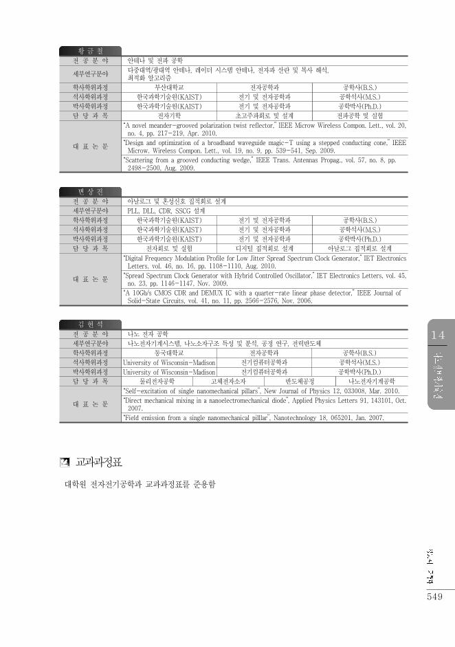
황 금 철전 공 분 야 안테나 및 전파 공학세부연구분야 다중대역/광대역 안테나, 레이더 시스템 안테나, 전자파 산란 및 복사 해석,최적화 알고리즘학사학위과정 부산대학교 전자공학과 공학사(B.S.)석사학위과정 한국과학기술원(KAIST) 전기 및 전자공학과 공학석사(M.S.)박사학위과정 한국과학기술원(KAIST) 전기 및 전자공학과 공학박사(Ph.D.)담 당 과 목 전자기학 초고주파회로 및 설계 전파공학 및 실험
대 표 논 문
“A novel meander-grooved polarization twist reflector,” IEEE Microw Wireless Compon. Lett., vol. 20, no. 4, pp. 217-219, Apr. 2010.“Design and optimization of a broadband waveguide magic-T using a stepped conducting cone,” IEEE Microw. Wireless Compon. Lett., vol. 19, no. 9, pp. 539-541, Sep. 2009.“Scattering from a grooved conducting wedge,” IEEE Trans. Antennas Propag., vol. 57, no. 8, pp. 2498-2500, Aug. 2009.
변 상 진전 공 분 야 아날로그 및 혼성신호 집적회로 설계세부연구분야 PLL, DLL, CDR, SSCG 설계학사학위과정 한국과학기술원(KAIST) 전기 및 전자공학과 공학사(B.S.)석사학위과정 한국과학기술원(KAIST) 전기 및 전자공학과 공학석사(M.S.)박사학위과정 한국과학기술원(KAIST) 전기 및 전자공학과 공학박사(Ph.D.)담 당 과 목 전자회로 및 실험 디지털 집적회로 설계 아날로그 집적회로 설계
대 표 논 문
“Digital Frequency Modulation Profile for Low Jitter Spread Spectrum Clock Generator,” IET Electronics Letters, vol. 46, no. 16, pp. 1108-1110, Aug. 2010.“Spread Spectrum Clock Generator with Hybrid Controlled Oscillator,” IET Electronics Letters, vol. 45, no. 23, pp. 1146-1147, Nov. 2009.“A 10Gb/s CMOS CDR and DEMUX IC with a quarter-rate linear phase detector,” IEEE Journal of Solid-State Circuits, vol. 41, no. 11, pp. 2566-2576, Nov. 2006.
김 현 석전 공 분 야 나노 전자 공학세부연구분야 나노전자기계시스템, 나노소자구조 특성 및 분석, 공정 연구, 전력반도체학사학위과정 동국대학교 전자공학과 공학사(B.S.)석사학위과정 University of Wisconsin-Madison 전기컴퓨터공학과 공학석사(M.S.)박사학위과정 University of Wisconsin-Madison 전기컴퓨터공학과 공학박사(Ph.D.)담 당 과 목 물리전자공학 고체전자소자 반도체공정 나노전자기계공학
대 표 논 문“Self-excitation of single nanomechanical pillars”, New Journal of Physics 12, 033008, Mar. 2010.“Direct mechanical mixing in a nanoelectromechanical diode”, Applied Physics Letters 91, 143101, Oct. 2007.“Field emission from a single nanomechanical pilllar”, Nanotechnology 18, 065201, Jan. 2007.
교과과정표 대학원 전자전기공학과 교과과정표를 준용함


