EP-130_62315RevC.qxp_EP-130_062812 6/23/15 11:16 AM Page 1
-2-
TABLE OF CONTENTSBefore We Begin Page 4Installing the Batteries 4Making Wire Connections 5Components 5Building Your First Project 9Troubleshooting 10Helpful Suggestions 10
I. PLAYGROUND OF ELECTRONIC CIRCUITS 11 1. Woodpecker 12 2. Police Siren 13 3. Metronome 14 4. Grandfather Clock 15 5. Harp 16 6. Tweeting Bird 17 7. Meowing Cat 18 8. Calling’ Fish 19 9. Strobe Light 20 10. Sound Effects for Horror Movies 21 11. Machine Gun Oscillator 22 12. Motorcycle Mania 23 13. Vision Test 24 14. Patrol Car Siren 25
II. BASIC ELECTRONICS CIRCUITS 26A MAJOR CHANGE 27 15. Dimming the Light 28 16. Flip Flopping 29 17. Capacitor Discharge Flash 30 18. Transistor Action 31 19. Series and Parallel Capacitors 32 20. Transistor Switching 33 21. Series and Parallel Resistors 34 22. Amplify the Sound 35
III. LED DISPLAY CIRCUITS 36 23. LED Display Basics 37 24. Digital Display Circuit for the Seven-Segment LED 38 25. LED Display with CdS and Transistor 39 26. Switching the LED Display Using Transistor Control 40
IV. WELCOME TO DIGITAL CIRCUITS 41 27. “Flip-Flop” Transistor Circuit 42 28. “Toggle Flip-Flop” Transistor 43 29. “AND” Diode Transistor Logic with LED Display 44 30. “OR” DTL Circuit with Display 45 31. “NAND” DTL Circuit with Display 46 32. “NOR” Transistor Circuit with Display 47 33. “Exclusive OR” DTL Circuit 48
V. MORE FUN WITH DIGITAL CIRCUITS 49 34. “BUFFER” GATE using TTL 50 35. “INVERTER” GATE using TTL 51 36. “AND” GATE using TTL 52 37. “OR” GATE using TTL 53 38. “R-S Flip-Flop” using TTL 54 39. “Triple-Input AND” Gate using TTL 55 40. “AND” Enable Circuit using TTL 56 41. “NAND” Enable Circuit using TTL 57 42. “NOR” Enable Circuit using TTL 58 43. “NAND” Gate Making a Toggle Flip-Flop 59 44. “Exclusive OR” GATE using TTL 60 45. “OR” Enable Circuit using TTL 61 46. Line Selector using TTL 62 47. Data Selector using TTL 63
Important: If you encounter any problems with this kit, DO NOT RETURN TO RETAILER. Call toll-free (800) 533-2441 or e-mail us at: [email protected]. Customer Service • 150 Carpenter Ave. • Wheeling, IL 60090 U.S.A.
• Do not short circuit the batteryterminals.
• Never throw batteries in a fire orattempt to open its outer casing.
• Use only 1.5V “AA” type, alkalinebatteries (not included).
• Insert batteries with correct polarity.• Do not mix alkaline, standard (carbon-
zinc), or rechargeable (nickel-cadmium) batteries.
• Non-rechargeable batteries should notbe recharged. Rechargeable batteriesshould only be charged under adultsupervision, and should not berecharged while in the product.
• Do not mix old and new batteries.• Remove batteries when they are used
up.• Batteries are harmful if swallowed, so
keep away from small children.
WARNING: Always check your wiring beforeturning on a circuit. Never leave a circuitunattended while the batteries are installed.Never connect additional batteries or anyother power sources to your circuits.
WARNING:CHOKING HAZARD - Small parts.Not for children under 3 years.
Conforms to all applicable U.S. governmentrequirements.
Batteries:
!
EP-130_62315RevC.qxp_EP-130_062812 6/23/15 11:16 AM Page 2
-3-
VI. MEET TRANSISTOR-TRANSISTOR LOGIC 64 48. Blinking LEDs 65 49. Machine Sound 66 50. Astable Multivibrator Using TTL 67 51. Tone Generator 68 52. Monster Mouth 69 53. Dark Shooting 70 54. A One-Shot TTL 71 55. Transistor Timer Using TTL 72 56. LED Buzzing 73 57. Another LED Buzzing 74 58. Set/Reset Buzzer 75 59. Another Set/Reset Buzzer 76
VII. OSCILLATOR APPLICATION CIRCUITS 77 60. Ode to the Pencil Lead Organ 78 61. Double-Transistor Oscillator 79 62. Decimal Point Strobe Light 80 63. “The Early Bird Gets the Worm” 81 64. Adjustable R-C Oscillator 82 65. Heat-Sensitive Oscillator 83 66. Pulse Alarm 84 67. Pushing & Pulling Oscillator 85 68. Slow Shut-off Oscillator 86 69. Electronic Organ Detector 87
VIII. MEET THE OPERATIONAL AMPLIFIER 88 70. Operational Amplifier Comparator 89 71. Changing Input Voltage 90 72. Non-inverting Dual Supply Op Amp 91 73. Inverting Dual Supply Op Amp 92 74. Non-inverting Amplifier 93 75. Dual-Supply Differential Amplifier 94 76. Miller Integrating Circuit 95 77. Stable-Current Source 96 78. Operational Amplifier Blinking LED 97 79. LED Flasher 98 80. Double LED Blinker 99 81. Single Flash Light 100 82. Introducing the Schmitt Trigger 101 83. Initials on LED Display 102 84. Logic Testing Circuit 103 85. Voice-Controlled LED 104 86. Buzzing’ with the Op Amp 105 87. Sweep Oscillator 106 88. Falling Bomb 107 89. Alert Siren 108 90. Crisis Siren 109 91. Op Amp Metronome 110 92. Burglar Buzzer 111
93. LED Initials 112 94. Wake Up Siren 113 95. Voice Activated LED 114 96. Logic Tester 115
IX. MORE FUN WITH OPERATIONAL AMPLIFIERS 116 97. Voice Power Meter 117 98. Reset Circuit 118 99. RC Delay Timer 119 100. Listen To Alternating Current 120 101. Pulse Frequency Multiplier 121 102. White Noise Maker 122 103. Light-Controlled Sound 123 104. DC-DC Converter 124 105. Super Sound Alarm 125 106. Op Amp Three-Input “AND” Gate 126 107. Timer 127 108. Cooking Timer 128
X. RADIO AND COMMUNICATION CIRCUITS 129 109. Operational Amplifier AM Radio 130 110. AM Code Transmitter 131 111. AM Radio Station 132 112. Crystal Set Radio 133 113. Two-Transistor Radio 134 114. Morse Code Oscillator With Tone Control 135
XI. TEST AND MEASUREMENT CIRCUITS 136 115. Water Level Warning 137 116. Water Level Alarm 138 117. Audio Signal Hunter 139 118. RF Signal Tracer 140 119. Square Wave Oscillator 141 120. Sawtooth Oscillator 142 121. Audio Continuity Tester 143 122. Audio Rain Detector 144 123. Audio Metal Detector 145 124. Water Level Buzzer 146 125. Pule Tone Generator 147 126. Resistance Tester 148 127. Transistor Tester 149 128. Sine Wave Oscillator 150 129. Sine Wave Oscillator With Low Distortion 151 130. Twin-T Oscillator 152INDEX 153PARTS LIST 155DEFINITION OF TERMS 156IDENTIFYING RESISTOR VALUES 159IDENTIFYING CAPACITOR VALUES 159METRIC UNITS AND CONVERSIONS 159
EP-130_62315RevC.qxp_EP-130_062812 6/23/15 11:16 AM Page 3
Welcome to the thrilling world of electronics! Nowthat you have your Elenco® EP-130 ElectronicPlayground Kit, you can learn about electronics whiledoing 130 fun experiments. In this kit we haveincluded everything you will need to start off on thiselectronics adventure, well except the batteries thatis J. As you go through this manual and do theexperiments, you will notice that we have arrangedthe experiments, as well as information, into a logicalprogression. We will start off with easy circuits andthen work toward the more intricate ones. Take yourtime and be sure to have some fun! Each electronic component in the kit is connected tosprings, so you can do all the circuit assemblywithout having to solder. To build a working project,all you have to do is connect the wires to theterminals as shown in each wiring sequence. Thereis no danger when doing these projects because youare using low voltage batteries, not the standard ACvoltages. Our simple instructions will show you how to operatethe circuit for each experiment. A schematic diagramis also included, to help you learn how the circuitworks. A schematic is simply a blueprint that showshow different parts are wired together. An image orsymbols for each of the components in your kit areprinted next to each piece.
As you will notice we refer to a Volt / Ohm Meter(VOM) for making measurements. A VOM ormultimeter is a instrument that measures voltage,current (amperes or amps), and resistance (ohms-W). You will learn more about these in the upcomingpages. If you really want to learn about electroniccircuits, it is vital that you learn how to measurecircuit values - for only then will you reallyunderstand electronic circuitry. You do not have to have or use a VOM to do theexperiments but you will find that it helps to bettergrasp how the circuits work. The VOM is a goodinvestment if you plan to stay interested in electricityand electronics.
-4-
BEFORE YOU START THE FUN!
This kit requires six (6) “AA” batteries. To install thebatteries to the back of your kit make sure to installthem in the corresponding compartments. Put the +end and the – end correctly into the kit, the + end forthe battery is the side that has the metal cap.
Remember: Never leave a dying battery or deadbattery in your kit. Even if they are “leak-proof”, theystill have the potential to leak damaging chemicals.
INSTALLATION OF BATTERIES
+–
–+
–+
+–
–+
–+
+––
+
–+
+––
+
–+
EP-130_62315RevC.qxp_EP-130_062812 6/23/15 11:16 AM Page 4
-5-
Provided in your kit are spring terminals and pre-cutwires, make the wires snap together for your use inthe numerous projects. To join a wire to a springterminal, just directly bend the spring over to oneside and then install the wire into the opening.
When you have to join to two or three wires into asingle spring terminal, be sure that the first wire doesnot come loose when you attach the second andthird wires. The simplest way to do this is to place thespring onto the opposing side where you haveconnected the first wire.
Only insert the exposed or shiny part of the wire intothe spring terminal. The electrical connection will notbe made if the plastic part of the wire is inserted intothe terminal. Removing the wire from the springterminals is simply just bending each terminal andthen pulling the wires out of it.
If the exposed metal ends of some of the wires breakoff due to great use, you should just simply remove3/8” if the insulation from the wire of the broken endand then simply twist the strands together. Toremove the installation you can use either a wire-stripper tool or a simple penknife. Be extremelycareful when doing this because penknives areremarkably sharp.
WIRING CONNECTIONS
This kit has more than 30 distinct components. If thishappens to be your first time with electronics don’tfret over not knowing the difference between aresistor or a transistor, because the general purposeof each component will be described. The followingexplanations will help you comprehend what eachcomponent does and you will also gain moreknowledge of each component as you do eachexperiment. There is also a parts list in the back ofthis manual, that way you can compare the parts inyour kit with those recorded in the back.
Resistors: Why is the water pipe that goes to thekitchen faucet in your house smaller than the onefrom the water company? And why is the pipesmaller than the main water line that disburses thewater to your entire town? Because you don’t need alot of water. The pipe size controls the water flow towhat you really need. Electricity works in the samemanner, except that the wires have a minimalresistance that they would have to be particularly thinto limit the electricity flow. They would be solidenough to handle and break effortlessly. However,the flow of water through a large pipe could berestricted to by filling a part of the pipe with rocks (a
COMPONENTS
EP-130_62315RevC.qxp_EP-130_062812 6/23/15 11:16 AM Page 5
fine screen would keep rocks from falling over),which would prolong the flow of water but not stop itcompletely. Like rocks are for water, resistors work ina similar way. They regulate how much electriccurrent flows. The resistance, is expressed in ohms(W, named in honor of George Ohm), kilohms (kW,1,000 ohms) or megohms (MW, 1,000,000 ohms) isa determination of how much resistor resists the flowof electricity. The water through a pipe can beincreased by an increase in water pressure or theremoval of rocks. In a similar way you can increasethe electric current in a circuit by increasing thevoltage or by the use of a lower value resistor (thiswill be shown in a moment). Below the symbol for theresistor is shown.
Resistor Color Code: The method for marking thevalue of resistance on a part is by using coloredbands on each resistor. The representation of thefirst ring is the digit of the value of the resistor. Thesecond ring is a representation of the second digit ofthe resistors value. The third ring means that you towhich power of ten to multiply by, ( or the amount ofzeros to add). The fourth and final ring is arepresentation of the construction tolerance. Amajority of resistors have a gold band thatrepresents 5% tolerance. Simply this means that theresistor value is guaranteed to be 5% of the valuedmarked. See the color chart on page 159.
Variable Resistor (Control): The variable resistoris simply a control and this is required in manyelectric circuits. The variable resistor can be used asa light dimmer, volume control, and in many othercircuits when you are wanting to change resistanceeasily and quickly. A normal resistor is shown, thiscontains an additional arm contact that moves alongthe resistive material and can tap off the resistancedesired.
Capacitors: Capacitors move alternating current(AC) signals while prohibiting direct current (DC)signals to pass. They store electricity and canfunction as filters to smooth out signals that pulsate.Capacitors that are small are traditionally used inhigh-frequency applications such as radios,transmitters, or oscillators. Larger capacitorsordinarily reserve electricity or act as filters. Thecapacitance (capacity for storing electricity) of acapacitor is expressed in a unit known as farad. Anextremely large amount of electricity defines thefarad. Most of the value of capacitors ispredetermined in millionths-of-a-farad ormicrofarads.
Electrolytic - Electrolytic are the four largestcapacitors. They are marked with an “–”. There isonly one-way to connect them to the circuit, the +and the – wires must always go into the correctterminals.
Note - For safety, the electrolytic capacitors used inthe EP-130 are nonpolarized type.
Disc - Unlike the electrolytic above, these capacitorshave no polarity and can be connected in either way.
Tuning Capacitor: Ever wonder what that knob thatchanges the stations on your radio is? It’s a tuningcapacitor. When the knob is rotated, the capacitanceis changed. This alters the frequency of the circuit,letting through only one frequency and blocking outthe rest.
-6-
Disc Electrolytic
EP-130_62315RevC.qxp_EP-130_062812 6/23/15 11:16 AM Page 6
Diodes: Are like one-way streets. They allow thecurrent to flow in only one direction. There are threeof these in your kit. Your kit contains one silicon diode(marked Si) as well as two germanium diodes(marked Ge).
Transistors: Three transistors can be found in yourkit. The part that makes each transistor work is a tinychip, which is made of either germanium or silicon.There are a total of three connections points on eachtransistor. They are B, which stands for base, C,which stands for collector, and E, which stands foremitter. Mainly transistors are used to amplify weaksignals. Transistors can also be used as switches toconnect or disconnect other components as well asoscillators to permit signals to flow in pulses.
LEDs (Light Emitting Diodes): These are specialdiodes because they give off light wheneverelectricity passes through them. (The current canonly pass through in one direction—similar to“regular” diodes).
LED Digital Display: Seven Light Emitting Diodesare arranged to create an outline that can show mostletters of the English alphabet and all the numbers.An additional LED is added to represent a decimalpoint.
The “8” LED display is mounted on a board and toprevent burning out the display with excess current,permanent resistors have been wired in.
Integrated Circuit: The transistor was invented inthe 1940’s and after that the next big break throughin electronics was in the 1960’s with the inventionintegrated circuit or the ICs. The advantage of thisthat the equivalent of hundreds or even thousands oftransistors, diodes and even resistors can be placedinto one small package. Two types of ICs are used in this kit. They are thequad two-input NAND and the dual-operationalamplifier, and you will have the chance to learn moreabout these in a bit. Simple ICs will help you to understand enough tograsp the basic theories of more advanced ICs.
Cadmium Sulfide (CdS) Cell: This is what is knownas a semiconductor, which practically resistselectricity while it conducts. The resistance changesby the amount of light that is shined upon it.
-7-
PNP NPN
EP-130_62315RevC.qxp_EP-130_062812 6/23/15 11:16 AM Page 7
-8-
Antenna: This cylindrical component with a coil offine wire wrapped around it is a radio antenna. Ifyou’re wondering what the dark colored rod is, it’sactually mostly powdered iron. It’s also known as a“Ferrite Core”, which is efficient for antennas, andused in almost all transistor radios.
Transformer: Did you know that if you were to wraptwo wires from different circuits around different endsof an iron bar, and if you were to add current in thefirst circuit, it will magnetically create current in thesecond circuit? That’s exactly what a transformer is!Transformers are used to isolate parts of a circuit, tokeep them from interfering with each other. If the iron bar in a transformer were allowed to rotate,it would become a motor. However, if a magnetwithin a coil is rotating then an electrical current ismade; this is called a generator. Those two ideasmay not seem important but they are the foundationof the present society. Pretty much all of the
electricity used in this world is generated by hugegenerators, which are propelled by water pressure orsteam. Wires transport energy to homes andbusinesses where it will be used. Motors are used toconvert the electricity back into mechanical form sothat it can be used to drive machinery andappliances.
Speaker: Did you know that electrical energy isconverted into sound through a speaker? By using the
energy from an AC electrical signal it createsmechanical vibration. Sound waves, which arecreated by variations of vibrations and then travelacross the room. When you hear a sound it is actuallyyour ears feeling the pressure from the air vibrations.To operate a speaker a high current and a low voltageare needed, so the transformer will also be used withthe speaker. (A transformer can convert a high-voltage/low current to a low-voltage/high current).
Similar to the speaker, is the earphone. It is movableand more sensitive than the speaker, otherwise theyare the same. The earphone you will be using isefficient as well as lightweight and can be usedwithout taking away too much electrical energy fromthe circuit. Sound wise you will be using theearphone for weak sounds and for louder sounds thespeaker will be used.
Batteries: The battery holders that are used in thiskit are constructed to hold six (6) “AA” batteries.These batteries will be the supplier of all the powerused in your experiments. When you connect thewires to the batteries make sure that you onlyconnect the batteries to terminals noted. Terminals119 and 120 provide 3 volts while terminals 119 and121 provide 4.5 volts. Be aware that parts can bedamaged (burned out) if you connect too muchvoltage (you can get up to 9 volts from theconnections to the batteries) Be sure to make batteryconnections the right way.Caution: Make sure your wiring uses the correctpolarity (the “+” and “-” sides of the component)!Some parts can be permanently damaged if youreverse polarity.
EP-130_62315RevC.qxp_EP-130_062812 6/23/15 11:16 AM Page 8
-9-
Switch: You know what a switch is – you useswitches every day. When you slide (or flip) to theproper position, the circuit will be completed,allowing current to flow through. In the other positiona break is made, causing the circuit to be “off”. Theswitch that we will be using is a double-pole, double-throw switch. You will learn about that later on.
Key: The key is a simple switch—you press it andelectricity is allowed to flow through the circuit. Whenyou release it, the circuit is not complete because abreak is caused in the circuit’s path. The key will beused in most circuits often times in signaling circuits(you can send Morse code this way as well as otherthings).
Terminals: Two terminals will be used in someprojects (terminals 13 and 14). They will be used tomake connections to external devices such as anearphone, antenna or earth ground connection,special sensor circuits and so forth.
Wires: Wires will be used to make connections tothe terminals. Your parts and spring terminals are mounted on thecolorful platform. You can see how the wires areconnected to the parts and their terminals if you lookunder the platform.
YOUR FIRST PROJECTA simple wiring sequence is listed for each project.Connect the wires with appropriate length betweeneach grouping of terminals listed. When doing theexperiment use the shortest wire that possibly getsthe job done. New groupings will be separated by acomma, connect the terminals in each group.As an example, here is the project 1 wiringsequence:1-29, 2-30, 3-104-106, 4-28-124, 5-41-105, 27-88,75-87-103-40, 115-42-119, 76-116, 121-22.
Connect a wire between 1 and 29, another wirebetween 2 and 30, another between 3 and 104 andthen another wire between 104 and 106. Continueuntil all connections are made.Caution: The last connection in each wiringsequence is an important power wire; this isdeliberate. It is important that you make thisconnection your LAST connection. Damage canoccur if one part of the circuit is completed beforeanother. Therefore follow the wiring sequenceexactly.
EP-130_62315RevC.qxp_EP-130_062812 6/23/15 11:16 AM Page 9
-10-
SUGGESTIONS TO HELPKeep a NotebookAs you’re about to find out, you are going to learnmany things about electronics by using this kit. Asyou learn, many of the things you discover in theeasy projects will be built upon in later projects. Wesuggest using a notebook to help you organize thedata you will be collecting. This notebook does not have to be like the one youuse in school. Think of it more as a fun notebook,that way you can look back on the all the projectsyou have done once you finish.
Wiring Sequence MarkingWhen you are wiring a project, especially those withlots of connections, you will find it helpful to mark offeach terminal number as you connect the wires to it.Use a pencil and make light marks so that you cango back multiple times and re-read the sequence.
Collecting ComponentsYou should start to make your own collection ofelectronic parts and therefore have your own scrapbox of electronic parts. You can build your owncircuits in or on top of a framework, box or container.You could use your circuit as a Science Fair projectat school and even make a major research projectfrom it.
TROUBLESHOOTINGYou should have no problem with the projectsworking properly if you follow the wiring instructions.However, if you do encounter a problem you can tryand fix it by using the following troubleshootingsteps. These steps are comparable to those stepsthat electronic technicians use to troubleshootcomplex electronic equipment.
1. Are the batteries being used new? If they are not,this may be your problem because the batteriescould be too weak to power the project.
2. Is the project assembled properly? Check all thewiring connections to make sure that you have allthe terminals wired correctly. Sometimes havingsomeone else look at it helps to find the problem.
3. Are you following the schematic diagram and theexplanation of the circuit? As your understandingand knowledge expands of electronics, you will beable to troubleshoot by following only a schematic,and once you add the description of the circuit youwill be able to figure out your own problems.
4. If you have VOM, try taking some measurementsof the voltage and current. You might be surprisedjust how handy a VOM really is.
5. Try building project 24 (Digital Display Circuit forthe Seven-Segment LED). This is a very simplecircuit that lights part of the LED display using only2 wires.
Contact Elenco® if you still need help.
EP-130_62315RevC.qxp_EP-130_062812 6/23/15 11:16 AM Page 10
-11-
I. PLAYGROUND OF ELECTRONIC CIRCUITS
EP-130_62315RevC.qxp_EP-130_062812 6/23/15 11:16 AM Page 11
-12-
For your first experiment you are going to make acircuit that sounds like a woodpecker chirping.Follow the wiring sequence carefully and observethe drawings. Don’t forget to make all the properconnections and have fun!The simple circuit shown here does not have a keyor a switch, but you can easily add one. Replaceconnection 124-28 with connections 124-137 and138-28 to connect the key. Or, you can hook theswitch up by replacing 124-28 with connections124-131 and 132-28. Now you can easily turn offand on the circuit. Go outside and see if you canattract birds with it.Want a different sound? Try varied combinations ofcapacitance and resistance in place of the 100mFcapacitor and the 1kW resistor. To change the100mF capacitor to 470µF, disconnect terminal 116and transfer to terminal 118. Then, reconnect thewire from 115 to connect to 117. Your “bird” mightsound like a cricket, or a bear! Also, you can try using the 3V power supply.Disconnect terminal 119 and connect it to terminal123. Now your bird might sound like an Englishsparrow. Feel free to experiment. Just don’t replacethe 47kW resistor with anything below 10kW,because it might damage the transistor.
EP-130_62315RevC.qxp_EP-130_062812 6/23/15 11:16 AM Page 12
-13-
Here is the first siren you are going to do – don’t beshocked if this experiment becomes the mostfamous circuit in this kit.This siren sounds like a real siren on a police car!After the wiring is competed press the key. The toneyou eventually hear gets higher after pressing thekey. When you release the key, the tone gets lowerand then fades out.Try some of these modifications: 1. If you change the 10mF capacitor to a 100mF or a
470mF it will give a very long delay for both turnoff and turn on.
2. Change the circuit to remove the delays bytemporarily disconnecting the 10mF capacitor.
3. Change out the 0.02mF capacitor to a 0.01mFcapacitor, and then to a 0.05mF capacitor.
Notes:EXPERIMENT #2: POLICE SIREN
Wiring Sequence:
o 1-29o 2-30o 3-103-109o 4-119-137o 5-47-110o 46-104-90o 114-48-120o 85-138o 86-89-113
Schematic
EP-130_62315RevC.qxp_EP-130_062812 6/23/15 11:16 AM Page 13
-14-
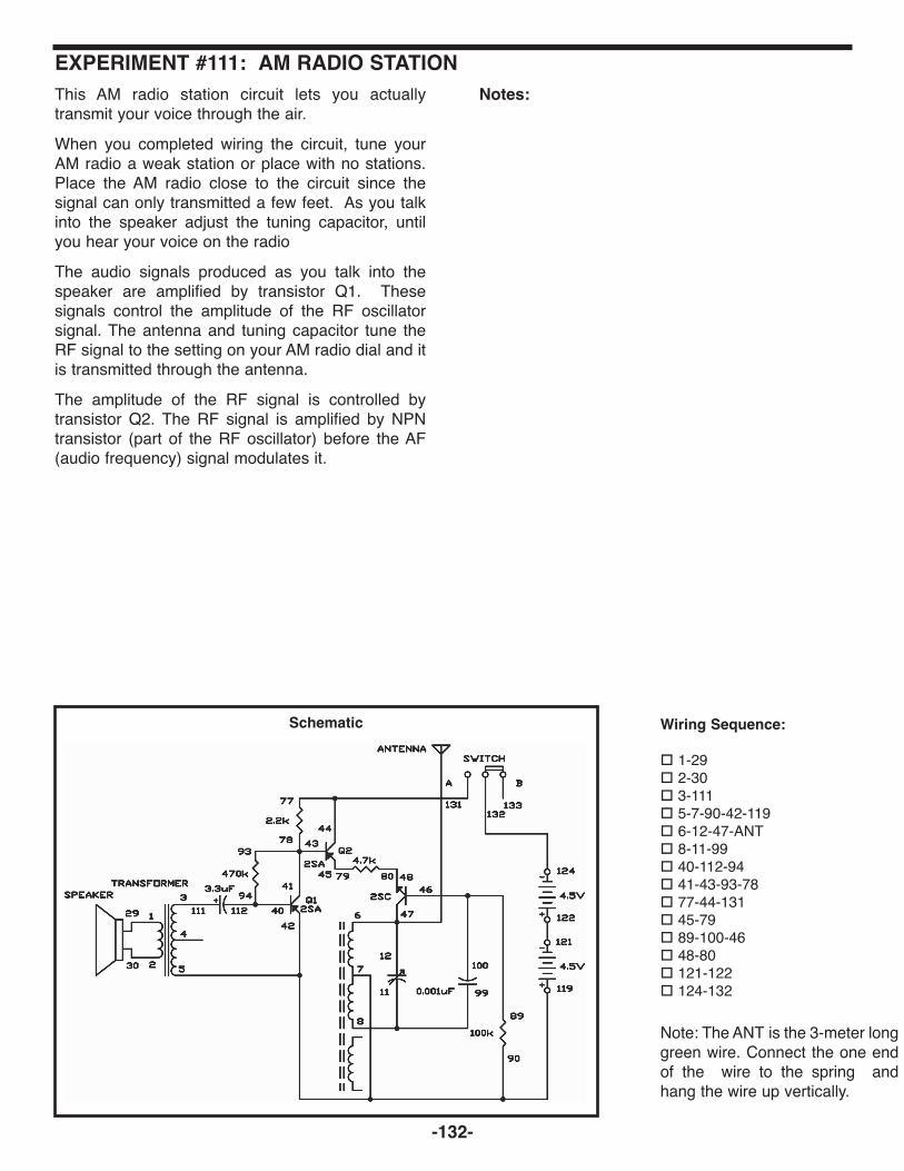
Learning to play a musical instrument? Then youmight find this experiment helpful. This is anelectronic version of the metronome, used bymusical students and musical geniuses alike,worldwide.If you press the key, you hear a repeating soundfrom the speaker. Turn the control knob to the rightand you’ll hear the sound “get faster” as the timebetween sounds shortens.Try swapping out the 4.7kW resistor with differentone. Also, you might want to try a different capacitorin place of the 100mF capacitor too see what effectit will have. Are you still keeping notes?If you would like to hear the difference that astronger capacitor makes, try connecting the 470mFcapacitor to the batteries. Connect terminal 117 to119 and terminal 118 to terminal 120. You mightneed to adjust the control to maintain the samepulse rate.
Notes:EXPERIMENT #3: METRONOME
Wiring Sequence:
o 1-29o 2-30o 3-104-116o 4-28-138o 5-41-103o 27-80o 40-115-79o 42-119o 120-137
Schematic
EP-130_62315RevC.qxp_EP-130_062812 6/23/15 11:16 AM Page 14
-15-
Does your home lack a grandfather clock? Well notany longer, with this experiment you will make yourown electronic grandfather clock.This circuit will produce clicks at approximately one-second intervals. The sound and timing togethermight remind you of an old grandfather clock. If youwould like for it to go faster or slower then you canchange out the 100kW resistor.The steady ticking can put animals (and people) intoa sleepy state of mind. If you have ever traveled ona train, you remember how sleepy you get fromhearing the clicking sound of the wheels. Ever scare a clock out of ticking? Shout directly intothe speaker. You can briefly stop the clock! Thespeaker acts like a microphone as well. The soundof your voice vibrates the speaker and disturbs theelectrical balance of the circuit, briefly.
Notes:EXPERIMENT #4: GRANDFATHER CLOCK
Wiring Sequence:
o 1-29o 2-30o 3-104-116o 4-90-120o 5-41-103o 40-72o 42-119o 71-89-115
Schematic
EP-130_62315RevC.qxp_EP-130_062812 6/23/15 11:16 AM Page 15
-16-
Have you ever wanted to make music just bywaving your hand? Well that is just what you aregoing to be doing. How does this magic work? Well,the tones change based upon the amount of lightthat gets to the CdS cell. With a bright light the toneis higher but, if you cover the CdS with your hand,the sound gets lower.Since the early days of vacuum-tube circuitry, thismethod of creating musical sound has been used.Leon Theremin was the inventor of this type ofinstrument, thus the instrument has been namedthe Theremin in his honor. After the wiring has been completed press the keyand then wave your hand over the CdS cell. You willsoon be able to play music with this magicalelectronic instrument after just a bit of practice. Mostimportantly HAVE FUN!
Notes:EXPERIMENT #5: HARP
Wiring Sequence:
o 1-29o 2-30o 3-16-41-109o 4-120o 5-106-110o 15-87o 40-105-88o 42-137o 119-138
Schematic
EP-130_62315RevC.qxp_EP-130_062812 6/23/15 11:16 AM Page 16
-17-
In this experiment you are going to make a circuitthat sounds like the mockingbird.Follow the wiring sequence and observe thedrawings. Don’t forget to make all the properconnections and have fun!To finish the circuit below, slide the switch to the Aposition to turn on the power. No sound will comefrom the speakers yet. When you press the key youwill hear a sound quite like a bird singing from thespeaker. When you release the key, you will still beable to hear the chirping sound but eventually it willslow down and stop. The first transistor “Q1” isdropped off from the battery when the key isreleased. Transistor “Q2” still produces the birdsound until the controlling current from transistor“Q1” stops.Try using a different value capacitor instead of the10mF and the 100mF capacitors. These capacitorscontrol the amount of electricity reaching thetransistors. Listen for the difference. Make sure tostart keeping notes on your experiments.
EP-130_62315RevC.qxp_EP-130_062812 6/23/15 11:16 AM Page 17
-18-
Are you bothered by mice, do you not have amousetrap? You should try this next experiment tohelp you instead—see if the sound of this cat cankeep the pests out of your life.Just follow the drawing below and the wiringsequence. To start the experiment switch the set toB. Press down on the key and release itimmediately. You will hear the meow from the catcoming from the speaker. If you adjust the controlknob while the cat’s meow is fading away, whateffect on the circuit operation does it have? Now setthe switch to A and try it once more. Now it soundsas if the cat is begging for a dish of milk in a low,long sounding tone.To produce a variety of sounds try experimentingwith this circuit. Whatever you do just don’t changethe value of the 0.05mF capacitor to more than 10mFor reduce the value of the 10kW resistor— or elsethe transistor could get damaged.
EP-130_62315RevC.qxp_EP-130_062812 6/23/15 11:16 AM Page 18
-19-
Did you know that many marine animalscommunicate to each other using sound? I bet youhave heard that dolphins and whales use sound forcommunication, but what you probably don’t knowis that they are not the only ones. Due to researchwe are able to find out that some fish are attractedto certain sounds. Making this circuit, will allow youdo to some research of your own.Once you make the last connection you are turningon the power. You should be able to hear pulses ofsound coming from the speaker. The soundchanges by turning the control. This circuit is a typeof audio oscillator circuit, which you will learn moreabout later in this book.If you have a fish tank at home or at school youshould place your kit near the glass to see if the fishare attracted to the sound. Are they?If you like to fish, you should try this out whilefishing. What you need to do is attach anotherspeaker to terminals 1 and 2 using long lengths ofinsulated wire. Wrap the speaker carefully in awaterproof plastic bag or place it in a tightly sealedjar. Make sure that no water is able to reach thespeaker. Lower the speaker into the water, cast yourfishing line, and see if you catch anything.
Notes:EXPERIMENT #8: CALLING’ FISH
Wiring Sequence:
o 1-29o 2-30o 3-93-100-110o 4-120o 5-41-109o 27-94o 28-40-99o 42-119
Schematic
EP-130_62315RevC.qxp_EP-130_062812 6/23/15 11:16 AM Page 19
-20-
In this experiment you will be creating an oscillatorcircuit that doesn’t make sound using a speaker oran earphone. Instead the circuit will produce lightwith an LED. This will give you an idea of howlarger strobe lights work. When you press the key,watch LED 1. At certain intervals the light turns onand off. With the 50kW control you can control therate of blinking.Try substituting a capacitor with a lower value forthe 100mF capacitor to see how an oscillator works.Make a prediction about what you think willhappen? Were you correct?
Notes:EXPERIMENT #9: STROBE LIGHT
Wiring Sequence:
o 3-115o 4-27-138o 5-31o 28-80o 33-47o 79-116-112-46o 111-48-121o 119-137
Schematic
EP-130_62315RevC.qxp_EP-130_062812 6/23/15 11:16 AM Page 20
-21-
The sounds that you will hear from this circuit willremind you of the music you hear in horror movies.Once you wire the project, use your special lightshield and your hand to change the light amountthat shines onto the CdS cell. This changes thepitch of the music.The pitch of a sound is determined is by the soundwave’s frequency, which is the number of cycles ofelectromagnetic energy per second. The amount oflight on the CdS cell determines the resistance ofthe cell. The more resistance you have the slowerthe frequency of the musical sound waves. Theoscillator circuit produces the basic sound wave.
Frequency modulation, or FM, is when thefrequency of an oscillator is controlled by part of thecircuit. An FM radio signal is similar to this but athigher frequencies.
EP-130_62315RevC.qxp_EP-130_062812 6/23/15 11:17 AM Page 21
-22-
This circuit is what engineers refer to as a “pulseoscillator”. It will make machine gun like sounds.There are many different ways to make oscillators.In this kit, you will build several of them and later on,you will be told on how they work. In the meantime,we will just tell you what an oscillator is.An oscillator is a circuit that goes from high to lowoutput on its own, or in other words, it turns itself onand off. A pulse oscillator is controlled from pulses,like the pulses made from a capacitor charging anddischarging. The oscillator in this kit turns off and onslowly. However, some oscillators turn off and onmany thousands of times per second. Sloweroscillators can often be seen controlling blinkinglights, such as turn signals in a car or truck. “Fast”oscillators are used to produce sound. The fastestoscillators produce radio frequency signals knownas “RF signals”. The RF signal oscillators turn onand off millions of times per second!The amount of times an oscillator turns off and oneach second is called the frequency of the oscillator.Frequency is measured in units called hertz (Hz).The frequency of this oscillator is about 1 to 12Hz.The frequency of a radio signal oscillator would bemeasured in either MHz (megahertz, meaning amillion hertz) or kHz (kilohertz, meaning a thousandhertz).
Once you finish wiring, press the key to start theoscillator. The 50kW resistor is the control; you canswap it out with other resistors to change the soundfrom a few pulses per second to a dozen or so persecond. Also, you can change the frequency of thisoscillator circuit by swapping out other capacitors inplace of the 10mF. Remember to observe the correctpolarity!
EP-130_62315RevC.qxp_EP-130_062812 6/23/15 11:17 AM Page 22
-23-
Have you ever tried to steer a bicycle or amotorcycle with just four fingers? This would bedangerous on a real motorcycle but on electronicversion it is a lot of fun!To do this project, connect the componentsfollowing the wiring sequence. Next grasp the metalexposed ends of the two long wires (connected toterminals 110 and 81) in between your index fingerand thumb of your left and right hands. Now varyyour grip/pressure and listen as the sound changesin the speaker. Due to the grip you use the soundchanges. You can create different sounds by controlling thelight that into the CdS cell. If you have a strong lighton the CdS cell you can control the entire operationby putting more pressure on the wires within yourhands. Make a shadow over the CdS cell with yourhand and see what happens. By holding the ends of the wires, you are makingyourself an extension of the circuit- thus a humanresistor. When you change your grip the resistancechanges in the projects current. The sound from thecircuit will make a real motorcycle noise and withpractice you can do it real well. By doing this youcan make the motorcycle idle as well as race.
Experiment with different values for the 0.1mF and0.05mF capacitors, but make sure you don’t usevalues above 10mF or you may damage thetransistor.
Notes:
EXPERIMENT #12: MOTORCYCLE MANIA
Wiring Sequence:
o 1-29o 2-30o 3-16-105-109o 4-120o 5-41-106o 15-82o 40-110-WIREo 42-119o 81-WIRE
Schematic
WIRE
EP-130_62315RevC.qxp_EP-130_062812 6/23/15 11:17 AM Page 23
This circuit produces short pulses. After you closethe key, the LED display shows 1 for a second andthen turns off, even when you keep pressing the key.You could create a game with this circuit. Display anumber or a letter on the LED display and then havethe players tell you what number it is. You changenumbers or letters on the display by just changingthe wiring to the display. Connect the terminals toform the letters or numbers to terminal 71 (in theplace of the 21 and 23 terminals). Connections forthe number 3 would be 17-21-22-23-20-71.You can try different values of capacitors to see theireffects. Don’t use a capacitor with a value higherthan 10mF or the excessive current can damage thetransistor.
Notes:EXPERIMENT #13: VISION TEST
Wiring Sequence:
o 21-23-71o 25-124-137o 40-73o 41-72o 82-83-42-119o 74-81-111o 84-112-138o 121-122
-24-
Schematic
EP-130_62315RevC.qxp_EP-130_062812 6/23/15 11:17 AM Page 24
-25-
With this experiment you may want to be careful notto confuse your neighbors. This experiment soundsas like a loud siren just like the real sirens on policecars and ambulances. The tone is initially high butas you close the key the tone gets lower. You areable to control the tone just as the police andambulance drivers do.The oscillator circuit being used is the same typeused in many other experiments in this kit. Press thekey and another capacitor is added to the circuit toslow the action of the oscillator circuit.
Notes:EXPERIMENT #14: PATROL CAR SIREN
Wiring Sequence:
o 1-29o 2-30o 3-104-106-110o 4-85-120o 5-41-109o 40-137-105-86o 103-138o 42-119
Schematic
EP-130_62315RevC.qxp_EP-130_062812 6/23/15 11:17 AM Page 25
-26-
II. BASIC ELECTRONICS CIRCUITS
EP-130_62315RevC.qxp_EP-130_062812 6/23/15 11:17 AM Page 26
-27-
Until now, in addition to the wiring sequences you havehad drawings to help guide you in the wiring connections.The rest of the projects will have just the schematicdiagram without the circuit drawings.A schematic diagram is like a road map but it is used forelectronic circuits. It shows you how different partsconnect together and how electricity flows through acircuit. Electronics engineers and technicians useschematics to help guide them through circuits. You don’t need to build your circuits from the schematicdiagrams by themselves. We have added the number ofterminals to where you will be making the wiringconnections on each schematic, to help you out - a linebetween numbers on the schematic means that youshould connect a wire between those terminals in yourkit. Every part in your kit has a schematic symbol all of itsown. At the beginning of this manual you will find apicture of each part with its schematic symbol as well asa short description.
As you will start to notice, the schematics have somelines that cross each other and that there is a dot at thecrossing point. This means that the two wires which arerepresented by the lines, are to be connected at the pointwhere the dot is located (you will find the terminal numbernext to the dot). If there is not a dot where the lines cross,this means that the wires do not connect (you won’t seea terminal number if the wires don’t cross).
Lines Are Connected / Lines Not ConnectedThe schematic diagrams will look confusing at first butthey are simple once you have some practice usingthem. Don’t get discouraged if you get confused at first.You will be constructing circuits in no time by just lookingat the schematic diagrams. To be able to read schematic diagrams is important foranyone getting into the field of electronics. Manyelectronics books and magazines display intricate circuitsonly in schematic form. A schematic is also shorter andmore accurate way to show a circuit rather than a writtenform.
A MAJOR CHANGE
EP-130_62315RevC.qxp_EP-130_062812 6/23/15 11:17 AM Page 27
-28-
Ever thought you could use a capacitor to dim alight? Try this project. After you finish the wiring, setthe switch to A. Then the LED segments will light upslowly and show an L. Once the LED reaches itsbrightest point it will stay on. Move the switch to Band watch as the L fades away.Look at the schematic. When the switch is on, thecurrent flows from the battery to the 100mFcapacitor to charge. Once the capacitor reaches fullcharge, electricity flows to the transistor base andturns it on gradually, which turns the LED on.Eventually the capacitor will be completely chargedand then the current flows continuingly to the baseof the transistor and the LED stays on.When the switch is turned off and you remove thebattery from the circuit, then the capacitor starts todischarge through the transistor and the LED. The Ldims until the discharge of the 100mF is finished.If you want a slower dimmer circuit, all you have todo is replace the 100mF capacitor with the 470mFcapacitor. Replace connections 25-116-124 withconnections 25-118-124. Be patient because theLED does eventually come on.Go back to project 2 (the police siren) and see if youcan figure out why the siren goes from high to lowas you press and then release the key.
Hint: the 10mF capacitor charges when you closethe key.
Notes:
EXPERIMENT #15: LIGHT DIMMER
Wiring Sequence:
o 18-19-20-48o 25-116-124o 46-115-90o 119-47-131o 89-132o 121-122
Schematic
EP-130_62315RevC.qxp_EP-130_062812 6/23/15 11:17 AM Page 28
-29-
How about we take a break? This circuit is forentertainment. The numbers 1 and 2 will flash onthe display in the circuit. This might remind you ofsome neon signs that have eye-catchingadvertisements on them.A “flip-flop” circuit controls the LED display in thisexperiment. In later projects you will be learningmore about flip-flop circuits. Try a different value forthe capacitors to see the effects on the operationspeed. Try and rewire the LED display to flashnumbers other than 1 and 2. Try placing highervalues in place of the 22kW and 4.7kW resistors. Donot use lower values for any of the resistors or elseyou could damage the transistors.
Notes:EXPERIMENT #16: FLIP FLOPPING
Wiring Sequence:
o 17-19-20-22-41-116-82o 21-42-45-119o 23-44-118-84o 79-81-83-85-25-124o 80-117-40o 86-115-43o 121-122
Schematic
EP-130_62315RevC.qxp_EP-130_062812 6/23/15 11:17 AM Page 29
-30-
In this circuit single pulses of high voltage electricenergy are generated by suddenly discharging acharged capacitor through a transformer.Automobile ignition systems use a similar capacitor-discharge reaction.The operation of this circuit is simple but theconcepts involved are important to helping youunderstand more complicated circuits. If you haveaccess to an oscilloscope, you can scientificallymeasure the energy that is discharged through thetransformer. The 470mF capacitor stores up energy as thebatteries supply millions of electrons to thecapacitors negative electrode. Meanwhile thebatteries draw the same number of electrons fromthe capacitors positive electrode so that the positiveelectrode is lacking electrons. The current mustpass through the 4.7kW resistor, so it requires atleast 12 seconds for the capacitor to receive the full9V charge from the batteries.The amount of charge a capacitor can storedepends on its capacitance value and the voltageapplied across it. This represents the amount ofelectrons displaced in the electrode. The amount of electrons in a capacitor’s electrode ismeasured in coulombs. The quantity of onecoulomb is 6,280,000,000,000,000,000 electrons(6.25 x 10¹⁸).The charge in either electrode of the capacitor isdetermined by multiplying the capacitance (C) bythe voltage across the capacitor (E). (Q = C x E).The 470μF (470 x 10-6F) capacitor at 9V iscalculated as follows:
Q = C x E = 470 x 10-6 x 9 = 4.23 x 10⁻³ coulombsor:
470 x 0.000001 x 9 = 4.23 x 10⁻³ coulombs(265,564,400,000,000 electrons)
Pressing the key causes the above number ofelectrons to pass through the transformer winding ina very short time and induces a high voltage in thesecondary winding. Thus causing the LED to flash.An oscilloscope is an electronics measurementinstrument used by engineers and technicians. Ifyou have access to one, connect it (with help fromsomeone who knows how to use it) to terminal 3and terminal 5 of the transformer to indicate thepresence of 90V or more. The indicated voltage is
produced when the charge held by the capacitor isreleased into the transformer.
Notes:
EXPERIMENT #17: CAPACITOR DISCHARGE FLASH
Wiring Sequence:
o 1-138o 2-118-124o 3-31o 5-33o 79-119o 80-117-137o 121-122
Schematic
EP-130_62315RevC.qxp_EP-130_062812 6/23/15 11:17 AM Page 30
-31-
There are three connections made on a transistor;one of these (the base) controls the currentbetween the other two connections. The importantrule to remember for transistors is: a transistor isturned on when a certain voltage is applied to thebase. A positive voltage turns on an NPN typetransistor. A negative voltage turns on a PNP typetransistor.In this project the LED display shows whichtransistor is on by lighting either the top or thebottom half. This demonstrates how a positivevoltage controls an NPN transistor and the PNPtransistor is controlled by a negative voltage. After the connections are made the NPN transistorwill be turned on because the positive voltagethrough the 1kW resistor is applied to the base. Thisturns on the upper half of the LED display.Simultaneously the PNP is off because currentcannot flow to its base. (The current flows from thePNP emitter to the NPN transistor base; however,this flow from the PNP base is blocked by thediode.)The NPN is turned off if you press the key, becausecurrent is diverted away from its base. The PNP isturned on simultaneously because now current canflow from its base through the 4.7kW resistor. As aresult, the upper LED segments turn off and thelower segments turn on.
Notes:EXPERIMENT #18: TRANSISTOR ACTION
Wiring Sequence:
o 18-17-21-48o 19-20-23-41o 25-124-138o 40-80-77o 75-78-47-42-119o 76-46-126o 79-137-125o 121-122
Schematic
EP-130_62315RevC.qxp_EP-130_062812 6/23/15 11:17 AM Page 31
-32-
Some of the handiest items in your kit are thecapacitors. They store electricity, smooth outpulsing electricity into a steady flow and let someelectric current flow while blocking other current.This circuit allows you to compare the effects ofcapacitors connected in both series and parallel.Once you have finished wiring this project, set theswitch to B. Next connect terminals 13 and 14. Youwill hear a sound coming from the speaker. In thiscase, electricity is flowing through the 0.01mFcapacitor (refer to the schematic to help understandthis). Press the key now. What happens?You will hear a lower-pitched sound coming from thespeaker, because the 0.05mF capacitor has beenadded in parallel to the first capacitor. Current nowflows through both capacitors at the same time,through two channels that are separate. What doyou think happens to the total capacitance whenyou connect two capacitors in parallel?You may have guessed wrong. When connected inparallel, two capacitors make the total capacitanceincrease. The tone is lower because the increasedcapacitance causes it to be. Now release the key and then move the switch fromB to A. While the switch is set to A, do not press thekey. Now what do you hear?You now hear a high-pitched sound coming from thespeaker. This is due to the 0.05mF and 0.01mFcapacitors are now connected in series – the flow ofthe current goes directly from one to the other. Thetotal of the capacitance in the circuit is less than the
smallest capacitor in the series connection. Thehigher-pitch sound is caused by the lowercapacitance.
EP-130_62315RevC.qxp_EP-130_062812 6/23/15 11:17 AM Page 32
-33-
In this experiment you study the switching action oftransistors in turning an LED on. You will be usingtwo different transistors - one of the two PNP typesand the NPN type included in your kit. PNP and theNPN refers to the arrangement of thesemiconductor materials inside the transistors.The NPN transistor at the bottom of the schematicstays on due to the 47kW resistor supplying voltageto its base. Making the connection through the22kW resistor causes the PNP transistor at the topof the schematic to turn on. The resistance of the 22kW is approximately half ofthat of the 47kW resistor, so the current supplied tothe base of the PNP transistor is about twice that ofthe NPN. Therefore the PNP is turned on “greater”than the NPN. Connect the circuit and then press the key: 1 isdisplayed. To increase the base current for the NPNtransistor, you have to decrease the value of the47kW resistor connected to the base – terminal 46.To do this simply disconnect between 87 and 88 andthen replace them with connections to anotherresistor. For example, change connection 87-42 to83-42 and connection 46-88 to 84-46, to change the47kW to a 10kW resistor. Every time that you lowerthe resistor value more current is then supplied tothe base of the transistor, and the LED display lightsa little brighter when you press the key. If youdecrease the resistance below 1kW the transistormay burn out.
Next, change the resistors to 10kW and then pressthe key. Use terminals 83 and 84 and terminals 81and 82. With the transistors both fully on thebrightness should not change much. If change doesoccur check your batteries.
Notes:
EXPERIMENT #20: TRANSISTOR SWITCHING
Wiring Sequence:
o 21-23-41o 25-47o 40-85o 87-42-119o 46-88o 124-48-137o 86-138o 121-122
Schematic
EP-130_62315RevC.qxp_EP-130_062812 6/23/15 11:17 AM Page 33
-34-
In this project, you will discover what happens whenyou connect resistors in series and in parallel. Youwill see the LED-1 on the panel flash on and offwhen you finish wiring.See what happens to the LED on side A and then onside B when you slide the switch. There is nochange at all. The schematic shows that two 10kWresistors are connected in series to side A of theswitch, and one 22kW resistor is connected to sideB. The resistors connected in series on side A areequal to the sum of each resistor’s value – so 20kWis the total resistance of the resistors. This is aboutthe same as 22kW resistance in side B. So the LEDshows no change when you move the switch.The LED becomes brighter when you press the key.By looking at the schematic, you will see that resistorR1 (470kW) is connected to the LED in series. Theresistor controls the flow of current to the LED. Thetotal resistance decreases when you press the key,R1 and resistor R2 (100W) are connected in parallel.The LED becomes brighter because of the amountof current flowing to it increases, when the amount ofresistance decreases.Calculating the total resistance for resistorsconnected in parallel is not as easy as when resistorsare connected in series. You must multiply the values
together, and then divide the product by the sum ofvalues. In this case, the total resistance is:
Connect now terminals 13-14. As shown in theschematic, this connects the 22kW resistor inparallel with the two 10kW resistors. Is there anychange in the LED? The flashes on and off of theLED are at shorter intervals because the resistanceconnected to the slide switch decreases. Try tocalculate the new resistance value. The new valueis about 10.5kW.This circuit is known as a multivibrator. Amultivibrator is an oscillator that uses componentsthat direct current back to each other. From theschematic you can see that the 10mF and the 100mFcapacitors discharge through the transistors. Thismultivibrator circuit controls the oscillations tocreate the flash through the LED at certain intervals. You can now see that resistors and capacitors haveopposite effects when they are connected in seriesor parallel. Be careful - it is easy to get confusedabout which one increases or decreases instrength.
EP-130_62315RevC.qxp_EP-130_062812 6/23/15 11:17 AM Page 34
-35-
A two-transistor amplifier is used in this circuit. In anamplifier, a small signal is used to produce orcontrol a large signal. This circuit is similar to anearly model transistor hearing aid amplifier.Your kit’s speaker can change sound pressure intoa weak voltage. The transformer increases thevoltage, and which is then applied to the NPNtransistor through the 3.3mF capacitor. Now it is time to talk about the transformer. Thetransformer has a copper wire wound hundred ofturns. We call this a coil. A transformer has two coilsseparated by an iron plate. A magnetic field is created when electricity flowsthrough a coil. The reverse is also true - if a coil issubjected to a change in its magnetic field strength,electricity flows through it. The magnetic fieldcreated depends on the number of windings in thecoil, so when electricity flows through the first coil(the primary coil), the voltage at the second coil (thesecondary coil) will be different if the number ofwindings is different. Induction is the creation of anelectric charge using a magnetic field. Now go backto project 17 and think of how a large voltage isinduced at the secondary side when 9V is applied tothe primary side of the transformer.
EP-130_62315RevC.qxp_EP-130_062812 6/23/15 11:17 AM Page 35
-36-
III. LED DISPLAY CIRCUITS
EP-130_62315RevC.qxp_EP-130_062812 6/23/15 11:17 AM Page 36
-37-
By using the LED display you will see the effect ofelectrical signals. An LED is similar to a normaldiode except when current flows through it, it emitslight. One example of the LED display is a powerindicator on your DVD player or your radio that tellsyou the power is on.A seven-segment LED display can show thenumbers 0 through 9 for reading information on acalculator. Seven is the minimum number ofsegments (separate lines that can be each lighted)that are necessary to clearly distinguish all tendigits. Two conditions that you must always observefor the proper LED operation are:1. Polarity correctness (+ and – LED connections) 2. Proper current flow LEDs can burn out due to reverse polarity if thevoltage is more than about 4 volts, or if the currentis not limited to a safe value. When the polarity isreversed the LED will not light. Series resistors (permanently wired to your kit) areused with the LED display to keep the current flowat a proper level. Current flows through theseresistors and the LED to terminal 25, providing acomparatively constant voltage (approx. 1.7 volts)to the LED. To make the current flow through theLED display we need voltages above this value.The series resistors set how much current flowsfrom the batteries through the LED.Now it is time for you to learn about the common-cathode seven-segment LED digital display. SevenLED display segments use one contract point –terminal 25 – as a common negative electrode in acommon- cathode. To allow current to flow through an LED must haveboth (+) and (–) connections. The anode is thepositive side and the cathode is the negative side.In this kit the LED display is a common cathodetype. You connect any anode segment terminals asrequired, to the battery’s positive side and connectthe common cathode segment terminal (terminal25) to the negative side of the battery.LEDs operate tremendously fast. An LED can turnoff and on hundreds of times per each second; sofast that you won’t even see it blink. There is nowarm up time or large amount of heat producedunlike an incandescent lamp.
Do the following experiment to experience how fastthe LED operates.1. Do not close the key but hook up the circuit.2. Decrease the light in the room to a low level so
that you are able to see the LED light emissioneasily.
3. Close the key but only for less than a second.You will notice that the display goes quickly off andon. Hold the platform steady but glance quickly atthe LED as you quickly tap the key. It will appearthat the display goes on and off. What occurs in thepersistence of the human eye is much longer thanthe LED’s time but without the use of specialinstruments this gets the point across.
Notes:
EXPERIMENT #23: LED DISPLAY BASICS
Wiring Sequence:
o 17-18-19-20-21-22-23-24-138o 25-120o 119-137
Schematic
EP-130_62315RevC.qxp_EP-130_062812 6/23/15 11:17 AM Page 37
-38-
Wire the circuit as shown to connect the 3V supplyto the LED segments and the decimal point (Dp).What numbers and letters do you see displayed?In this experiment you can make some voltagemeasurements using a Voltage/Ohm Meter (VOM) ifyou have one. Connect the VOM as directed by itsinstructions. Skip these measurements if you do nothave a VOM.With this low battery voltage, you can reverse thepolarity of the circuit by reversing the connections tothe battery. (Changes to make are: change 25-120and 119-WIRE, 25-119 and 120-WIRE.) Recordyour results. After you note your results, reconnectthe battery with the correct polarity. Measure theLED voltages between terminal 25 and eachseparate terminal (17 through 24) using a VOM ifyou have one. Change the battery connections to25-124, 121-122, and 119-WIRE to temporarilychange the 9V supply. Next, make the samemeasurements. What amount is the LED voltageincreased by, from using this three-time increasefrom the battery? (A normal increase is 0.25V)Next, try measuring the voltage in each resistorattached to one of the LED segments. All of theresistors are 360W. The LED current is in milliamps(one-thousandths of an ampere) is calculated bydividing the voltage by 360W. The LED segmentcurrents are approximately ____ milliamperes (mA)with the 3V supply (3mA typically), and ____ mAwith the 9V supply.Make a chart of the connections required to display0 through 9 on the display in the space below.
Notes:EXPERIMENT #24: DIGITAL DISPLAY CIRCUIT FOR THE SEVEN-SEGMENT LED
Wiring Sequence:
o 25-120o 119-WIRE
or
o 25-120o 119-(17, 18, 19, 20, 21, 22, or 23)
Schematic
EP-130_62315RevC.qxp_EP-130_062812 6/23/15 11:17 AM Page 38
-39-
In this project you will see how to turn on an LED byusing a transistor and a CdS cell.Think of the CdS cell as a resistor that changes itsresistance based upon the amount of light that fallsupon it. In the dark the resistance is very high,around 5 megohms (MW, 5 million ohms); in brightsunlight, it can decrease to about 100W or less. To test this easily; just set your VOM to theresistance function and then connect it to the CdScell. Now hold you hand over the CdS cell and noteits resistance. Read the resistance again once youhave moved your hand. For a switch you can use the NPN transistor. Thistransistor turns on when sufficient positive voltage isapplied to its base. Positive voltage leads from thepositive terminal of the battery, then to the CdS cell,to the control, and then finally to the 10kW resistor. The amount of voltage applied to the transistor’sbase is determined by the total resistance value ofthe CdS, the control, and the 10kW resistor. Theamount of light striking the cell and the controlsetting change the base voltage - making it eitherhigh or low enough to turn on the transistor. Usingyour voltmeter on the control, try to change thecontrol position while casting a shadow over theCdS to verify the voltage change. When lightchanges over the CdS, adjust the control so that thetransistor turns on and off. Under bright light the circuit displays a 1. You canconnect the wires to display any number you desire.1 might be considered to be a binary digit, showinglogic “high” (H or ON), as indication of the presenceof a bright light on the CdS cell. Can you rewire thiscircuit to display another character to indicate thiscondition?
Notes:EXPERIMENT #25: LED DISPLAY WITH CdS AND TRANSISTOR
Wiring Sequence:
o 15-21-23-119o 16-28o 25-47o 124-26-48o 27-82o 46-81o 121-122
Schematic
EP-130_62315RevC.qxp_EP-130_062812 6/23/15 11:17 AM Page 39
-40-
This project shows how to control the LED displaythrough the use of transistors.This circuit is similar to the one in Project 18(Transistor Action). The differences between thesetwo are the position of the switch as well as thevalue of the resistor. In this project we use the basecircuit of the NPN transistor as a switch, in order tocontrol the cathode of the LED. Project 18controlled the LED from the anode (positive side).The transistors in this circuit act as switches. ThePNP transistor is always on, allowing the current toflow from the collector to the emitter, because asufficient amount of the negative voltage is appliedto its base through one of the 10kW resistors. Whenyou press the key the NPN transistor turns on,thereby applying sufficient positive voltage to itsbase, through the use of another 10kW resistor.When you close the key, then current can flow fromthe PNP’s emitter to its collector. Here are some important basic principles for you toremember:
• When negative voltage is applied to its base, aPNP transistor turns on; the current flows fromthe collector to the emitter.
• When positive voltage is applied to its base, aNPN transistor turns on; the current flows fromthe emitter to the collector.
Current can now flow through the NPN transistor,thus current can now travel a complete path - fromthe negative batteries side, to the NPN transistor, tothe common cathode terminal of the display, to thePNP transistor, to the positive side of the batteries –thus lighting the display.Turning on the LED with either of the transistorsmay not see important to you now. But, to peoplewho design computer circuits that are complicated,it is an easy way to control the circuits. Have you noticed that transistors switch on and offas fast as you press the key? These quick switchingallows operations to be performed quickly bycomputers. Transistors are many times faster thanhand operated switches or relays. Later you will seehow to delay this fast switching by using othercomponents.
Notes:EXPERIMENT #26: SWITCHING THE LED DISPLAY USING TRANSISTOR CONTROL
Wiring Sequence:
o 21-23-41o 25-47o 40-82o 119-42-137o 46-84o 124-48-81o 83-138o 121-122
Schematic
EP-130_62315RevC.qxp_EP-130_062812 6/23/15 11:17 AM Page 40
-41-
IV. WELCOME TO DIGITAL CIRCUITS
EP-130_62315RevC.qxp_EP-130_062812 6/23/15 11:17 AM Page 41
-42-
What is a flip-flop? It is a kind of circuit that changesback and forth between two states (on and off) atspecific intervals. It flips into one state and flopsinto another and so on.Two transistors, two capacitors and four resistorsare used by the flip-flop to turn on and off the LED.Each of the transistors are always in the opposingstate of each other; when transistor Q1 is on,transistor Q2 is off; when Q2 is on then Q1 is off.The change from on to off or off to on, happensquickly (in microseconds). Note the effect on theflashing rate of the LED when adjusting the control. To see how this circuit works, look at the schematic.Remember when voltage is applied to the base of atransistor, it turns on. On the negative side of thebatteries you have the two PNP transistorconnected through resistors. You may think thatboth transistors would always be on however, thereare two capacitors connected to the bases that aidthe cause of the flip-flop action.In order to explain the circuit, you should assumethat transistor Q1 is off. The 100mF capacitor will becharging and discharging through its base, so wecan say that Q2 is on. Transistor Q2 is kept on afterthe 100mF capacitor has discharged due to the47kW resistor and the control. Now the 10mFcapacitor has received a charge and is dischargingthrough the 4.7kW resistor, the battery and the Q2.(Remember that current can flow through thecollector to the emitter when transistor Q2 when it ison.) As long as the charge on the 10mF is highenough the Q1 transistor remains off.
Transistor Q1 turns on when the charge drops to aspecific point, the negative voltage from the 47kWresistor. Once Q1 turns on, and 100mF quickly startscharging and transistor Q2 turns off. With the Q2 off,its collector voltage rises toward the 9V of thebattery supply and thus the LED turns off. The Q1turns on fully through the fast charging of the 10mF.This flip occurs very fast. The circuit will eventually flop back to the originalstate to repeat the above action due to the 100mFdischarging through the Q2 transformer. Look back at the previous projects and try to locatewhere you have used this sort of circuit.
Notes:
EXPERIMENT #27: “FLIP-FLOP” TRANSISTOR CIRCUIT
Schematic
Wiring Sequence:
o 21-23-41-114o 75-81-87-25-27-124o 28-79-82o 40-115-80o 45-42-119o 43-88-113o 44-116-76o 121-122
EP-130_62315RevC.qxp_EP-130_062812 6/23/15 11:17 AM Page 42
-43-
Now it is time to step into the world of digital circuitsand learn some basics. A circuit that acts as aswitch to turn different components off and on is adigital circuit. In this section you will be dealing withdiode-transistor logic (DTL) circuits- these arecircuits that use diodes and transistors to turn thepower on and off.It doesn’t usually matter how much voltage isapplied to a digital circuit; what matters is whetherthe circuit is off (no voltage present) or on (presenceof voltage). When a circuit is off we describe it aslogic low or use the number 0. When a circuit isturned on we say logic high or use the number 1. A switch that turns circuits on and off is a toggleswitch. In this experiment we will use the flip-flopcircuit to work as a toggle switch. In this project,unlike others that you will be doing later, the circuitdoes not change until you tell it to.
Once you have completed the wiring, set the switchto A. The lower part of the LED lights up. Press thekey now. The upper section lights up while the lowersection shuts down. Every time you press the keythe LED sections will change, thus a flip and a flop. When a transistor is on and the other transistor isoff, it will stay either on or off until you tell it tochange. We can easily say that a flip-flop circuitremembers. Once you put a circuit into a certainsetting, it will stay that way until you tell it to change.Controlled by a single toggle signal, flip-flops canremember many things. This is also why computerscan remember so many things.
EP-130_62315RevC.qxp_EP-130_062812 6/23/15 11:17 AM Page 43
-44-
In this circuit you will first learn about the ANDcircuit. When all the connections to its terminals arelogic high (receiving voltage), the AND circuitproduces a high output.Make the connections in this circuit based upon thewiring sequence below. After that make theconnection to terminals 119 and 124 using terminalsA (126) and B (128) in different combinations tocomplete the circuit and to learn how an AND circuitworks. Terminal 124 provides logic high (voltage) whileterminal 119 provides logic low (no voltage) in thiscircuit. H is only shown on the LED after you haveconnected terminal A and terminal B to terminal 124(high terminal). If you make the connection of eitherterminal A or B or both to terminal 119 (low terminal)the LED will display nothing. For the combinedoutput (the LED) to read H (high), both A and B haveto be high. The PNP transistor stays off when either or both ofthe inputs are low (terminals 126 and/or terminal128 are connected to terminal 119), and whenpositive voltage is applied to the PNP transistorbase through the diode(s). The NPN transistor isalso off because the PNP transistor does notcomplete the circuit, and no current is supplied tothe NPN transistor base. Also remaining off is theLED due to the fact that the common cathodeterminal is not connected to the negative powersupply.
The base of the PNP transistor turns on when bothof the inputs are high and when both diodes supplynegative voltage to the base of the PNP transistor.In addition, the NPN transistor turns on and then thecurrent flows to the display to light the LED. Symbol AB is used to represent an AND functionthat mathematicians use. On the bottom right of thisschematic is the schematic symbol for the ANDcircuit.
Notes:
EXPERIMENT #29: “AND” DIODE TRANSISTOR LOGIC WITH LED DISPLAY
Wiring Sequence:
o 22-23-21-18-19-72o 25-47o 81-40-125-127o 41-83o 42-129o 46-84-85o 86-82-48-124o 71-130-119o 121-122o 126-(to 119 “HIGH” or 124 “LOW”)o 128-(to 119 “HIGH” or 124 “LOW”)
Schematic
EP-130_62315RevC.qxp_EP-130_062812 6/23/15 11:17 AM Page 44
-45-
This next circuit is a logic OR circuit. Are you able toguess how this circuit may work? Remember thatthe AND circuit produces high logic only wheninputs A and B are both high. In the OR circuit logichigh is produced when A or B receives a logic highinput.By connecting either terminal A or B to terminal 119(logic high terminal) the display will show H. Tryconnecting each of the terminals to terminal 119;then to terminal 124. What occurs? Whenconnected to H the output is high when either A or Bis connected. A+B is the symbol for this logicfunction. We won’t explain the entire operation for you herebecause this circuit is similar to project #29.Compare these two projects (29 and 32); then make
notes of their similarities and their differences. Onthe schematics diagram see if you can follow thecircuit.
Notes:
EXPERIMENT #30: “OR” DTL CIRCUIT WITH DISPLAY
Schematic
Wiring Sequence:
o 71-41o 72-19-18-21-22-23o 79-25-48-124o 81-47o 83-127-125o 84-80-46o 85-42-119o 86-82-40o 121-122o 126-(to 119 “HIGH” or 124 “LOW”)o 128-(to 119 “HIGH” or 124 “LOW”)
EP-130_62315RevC.qxp_EP-130_062812 6/23/15 11:17 AM Page 45
-46-
You will not be able to find the word NAND in yourdictionary (unless it is a computer or electronicdictionary). This term means inverted or Non-ANDfunction. It creates output conditions that are theopposite of the AND circuits output conditions.When both inputs A and B are high the NANDoutput is low. If either or both of the inputs are lowthen the output is high. The symbol for logic lookslike the AND symbol but with a small circle at theoutput. AB is the representation of the function.The NPN transistor stays off when either or bothterminals A and B are connected to terminal 124(logic low terminal), and negative current flowsthrough the diode(s). The LED remains off. Bothdiodes allow positive voltage to flow through themwhen both of the inputs are connected to terminal119 (logic high terminal). The NPN transistor isturned on by positive voltage, thus the current flowsto light the L on the LED.
Notes:EXPERIMENT #31: “NAND” DTL CIRCUIT WITH DISPLAY
Wiring Sequence:
o 81-20-19-18-119o 25-47o 82-46-128-126o 48-130o 121-122o 124-129o 125-(to 124 “LOW” or 119 “HIGH”)o 127-(to 124 “LOW” or 119 “HIGH”)
Schematic
EP-130_62315RevC.qxp_EP-130_062812 6/23/15 11:17 AM Page 46
-47-
It is easy to determine what the NOR (inverted OR)circuit does now that you have built and learnedabout the NAND (inverted AND) circuit. When eitherterminal A or B is connected to terminal H (119) thedisplay shows L. When low inputs are received byterminals both A and B then the circuit output ishigh. In the OR circuit this is the opposite. Theschematic shows the logic symbol for the NORcircuit. A + B is the writing for the function. The ORis symbolized by the + and the bar over the symbolsignifies that the circuit is inverted.The current path for the LED is complete when youconnect either A or B (or both) to terminal H, turningthe NPN transistor on. The transistor and the LEDgo off when you connect both A and B to L.
Notes:EXPERIMENT #32: “NOR” TRANSISTOR CIRCUIT WITH DISPLAY
Wiring Sequence:
o 18-19-20-119o 25-47o 46-82-84o 48-124o 81-(to 119 “HIGH” or 124 “LOW”)o 83-(to 119 “HIGH” or 124 “LOW”)o 121-122
Schematic
EP-130_62315RevC.qxp_EP-130_062812 6/23/15 11:17 AM Page 47
-48-
If you don’t know what an exclusive OR means,don’t worry. An exclusive OR (abbreviated XOR)circuit provides a high output only when one or theother of its inputs are high.You can see that an XOR circuit produces a lowoutput, only if both of the inputs are the same (highor low). If the inputs are different (either high andlow or low and high) it results in the output beinghigh. This circuit is handy to let us know if we havetwo inputs that are the same or if the inputs aredifferent. Before completing this circuit, be sure you have theswitch set to B. Once you have finished connectingthe wiring, connect terminals 13 and 14 to turn thepower on. Now watch LED 1. Press the key toproduce a high input. Is there any change in theLED 1? To make both inputs low release the switch.To make the input through the switch high, set theswitch to A. What does LED 1 do? Press the key while leaving the switch at A to makeboth the inputs high. Now you can see that in anXOR circuit, you need two high inputs to produce alow output. If desired, you can build an XNOR circuit (exclusiveNOR). We will not build one here, however, youmight be able to figure how to do it. Hint: It is almostidentical to the NOR circuit followed by additionalwiring in order to reverse the circuit. Make sure thatyou keep track of your experiments in yournotebook, particularly if you make an XNOR circuit.
EP-130_62315RevC.qxp_EP-130_062812 6/23/15 11:17 AM Page 48
-49-
V. MORE FUN WITH DIGITAL CIRCUITS
EP-130_62315RevC.qxp_EP-130_062812 6/23/15 11:17 AM Page 49
-50-
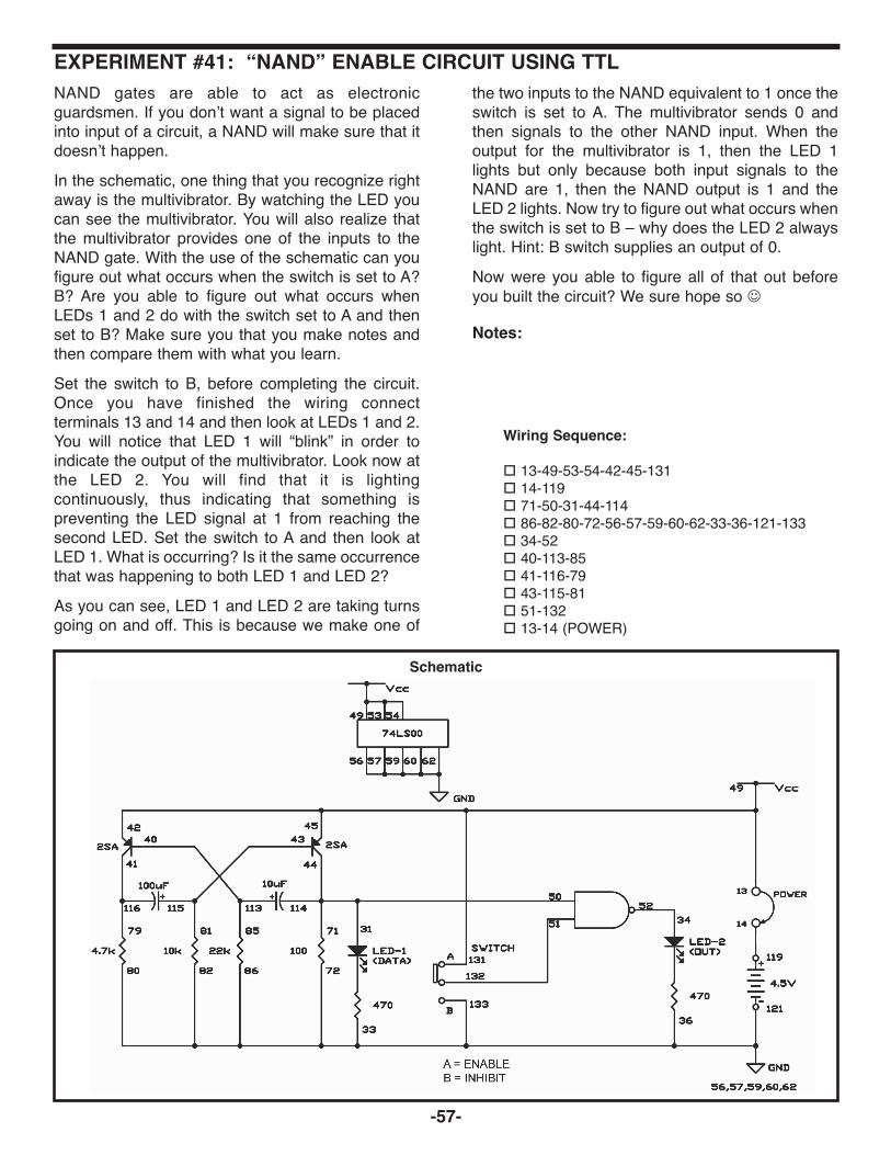
Have you ever wondered what happens once youstart adding digital circuits together, using the outputof one as the input of another? You’ll find out whenyou build this project.A quad two-input NAND gate IC, is one of theintegrated circuits contained in your kit. Some ofthese words will probably be a confusing at first. ICis short for integrated circuit. Something thatcontains many transistors, diodes, and resistors inone small package is an integrated circuit. ThisNAND gate uses TTL, short for Transistor-Transistor-Logic, because it is mostly constructedusing transistors. Quad means four. There are four separate NANDgate circuits, in this IC each receiving two inputs.Two input terminals are for Each NAND gate. As you build this project make sure to consult to theschematic. This circuit takes the output from oneNAND gate, and uses it for both inputs to thesecond (both inputs for the two NANDs are alwaysthe same here). What do you think happens if theinput to the first NAND is 1, after learning aboutNANDs? If the first input is 0? Attempt to figure it outbefore building this project.Set the switch to B before completing the wiring. Toturn the power on, connect terminals 13 and 14.What happens to LED 1? Set the switch to A. LED1 lights up.
1 is the input when the switch is set to A, and 0 isthe input when the switch is at B. When the input tothe first NAND is 1, its output is 0. But the 0 outputof the first NAND is the input to the second. The 0input to the second makes its output become 1,lighting the LED.
Notes:
EXPERIMENT #34: “BUFFER” GATE USING TTL
Wiring Sequence:
o 13-49-131o 14-119o 31-55o 33-56-57-59-60-62-133-121o 50-51-132o 52-53-54o 13-14 (POWER)
Schematic
EP-130_62315RevC.qxp_EP-130_062812 6/23/15 11:17 AM Page 50
-51-
A circuit that has an output that is the opposite of itsinput is called an inverter. If the output is 0, (low)then the input is 1 (high). If the output is 1, then theinput is 0.Before completing this project set the switch to A.Next, connect terminals 13 and 14. You’ll observethat both LED 1 and LED 2 are off. Since the inputis 1, the output has to be 0. When you set the switchto B, you will see both LEDs come on, indicating theinput is 0.You can see from the schematic that we use two ofthe four NAND gates in the IC. With the switch at A,both inputs to the two NANDs are 1. This means theoutputs of both NANDs are 0 (and the LEDs go out).When the switch is set to B, the LEDs come back onbecause we no longer have all inputs at 1. One extraordinary thing to think about is how big theRTL and DTL circuits were in earlier projects. Fourof those circuits, Believe it or not, have been shrunkdown to fit inside this tiny IC.ICs can be very complex. Large-scale integration(LSI) is the process of putting several circuits insidejust one IC. The microprocessors runningcomputers and cell phones are very complex ICs.
Notes:EXPERIMENT #35: “INVERTER” GATE USING TTL
Wiring Sequence:
o 13-49-50-131o 14-119o 31-52o 36-33-56-57-59-60-62-133-121o 34-55o 51-53-54-132o 13-14 (POWER)
Schematic
EP-130_62315RevC.qxp_EP-130_062812 6/23/15 11:17 AM Page 51
-52-
By using your kit’s NAND gates, are you able tofigure out how to make an AND gate? To find outlet’s experiment!As you build this circuit, leave the switch at B.connect terminals 13 and 14 to turn the power ononce you have finished. Now press the key. Whathappens to LED 1? Now while pressing the key, setthe switch to A. Are there any changes in LED 1?As you can observe by setting the switch to A andthen pressing the key, makes the inputs 1, causingthe overall output to be 1. Are you able to flow the 1input through the circuit until you reach a 1 output?Give it a try, but don’t peek at the answer.Here is how it works – each 1 input goes into thefirst NAND gate. Thus causing the output of theNAND to be 0. This 0 output is used for both inputsto the second NAND. The LED lights when the 0inputs to the second NAND cause its output to be 1.AND gate is formed from two NAND gates.
Notes:EXPERIMENT #36: “AND” GATE USING TTL
Wiring Sequence:
o 13-49-131-137o 14-119o 31-55o 72-56-57-59-60-62-33-133-121o 50-71-138o 51-132o 52-53-54o 13-14 (POWER)
Schematic
EP-130_62315RevC.qxp_EP-130_062812 6/23/15 11:17 AM Page 52
-53-
One of the cool things about the quad two-inputNAND IC is that to make up other logic circuits allwe have to do is combine the four NAND gates. Inour last two projects you have been shown how youare able to use NANDs to make up some other logiccircuits. In this project you will be shown how tomake up an OR gate from the NAND gates.Can you trace what happens from each input to theeventual output from just looking at the schematic?(Of course you can, just try it.)Keep the switch set to B, as you work on this project.Connect terminals 13 and 14 when you’ve finished.Now press the key. What happens to LED 1? Set theswitch to A and release the key. What happens toLED 1 now? Press the key again while keeping theswitch at A and press the key again. Are there anychanges in LED 1?You see that this circuit acts like other OR gatesyou’ve experimented with. The output to the LED is1 if at least one or the other of the inputs is 1. Haveyou tried tracing what happens from input to outputyet? The explanation is in the next paragraph.Say you press the key with the switch set to B. Thisenters 1 as both inputs of the NAND, thus causingthe NAND’s output to become 0. This 0 output isone of the inputs to the NAND gate controlling theLED. Since a NAND’s output is 0 only if all inputsare 1, then the 0 input causes the NAND’s output togo to 1, and LED 1 lights!
EP-130_62315RevC.qxp_EP-130_062812 6/23/15 11:17 AM Page 53
-54-
R-S does not mean Radio Shack® flip-flop. As wementioned earlier circuits that flip-flop alternatebetween two states. Those who use flip-flop circuitsmost often are engineers, and they use flip-flopcircuits to switch between low (0) and high (1)outputs. We say a circuit is at set status (S) whenthe output is high or on. We use the word rest (R)when a circuit is off.Once you have completed the wiring, to turn thepower on turn the switch to A. LED 1 or LED 2 willlight up. Touch terminals 13 and 14 in turn with thelong wire connected to terminal 26. What occurs toLED 1 and LED 2? The R-S flip-flop is set when the LED 2 lights. TheR-S flip flop is in reset when the LED 1 lights. Set orreset the flip-flop, then remove the long wire fromthe circuit and see what it does. Now you can observe one of the primarycharacteristics of the R-S flip flop. Once you havethe circuit either set or reset, the circuit stays in thespecific state until an input signal causes it tochange. This means that R-S flip flop can rememberthings. Advanced computers use similar circuits toremember things.
EP-130_62315RevC.qxp_EP-130_062812 6/23/15 11:17 AM Page 54
-55-
We have been using digital circuits that have twoinputs, but that doesn’t mean that we can’t havemore than the two inputs. Here is a TTL AND gatewhich has three inputs. Use the schematic to try andfigure out how to have three inputs result in anoutput of 1.We are going to do things a bit differently this time -terminals 13 and 14 create P as an input signal.When you connect the two terminals they create a 1input, and disconnecting them creates a 0.Connecting terminals 119 and 137 “turns on” thisproject.This circuit is called a gate because it is a circuit thathas more than one input and only one output. Theoutput of the gate is not energized until the inputsmeet the certain requirements. We will be using thishandy component in more digital circuits throughother projects.A gate circuit that is used to keep two portions of acircuit separated from each other is called a buffer. Next, look at the schematic and see if you can figureout the connections needed for the switch, the key,and terminals 13 and 14 that will result in an outputof 1. Try to figure it out on your own and then readon to see if you were correct.
The circuit works this way: connected to the oneNAND are both the key and the switch. When eachprovides an input of 1, then the NAND has an outputof 0. This 0 creates the input of another NAND,causing the output to become 1. This output of 1 then goes on to another NAND gate(can you find it on the schematic?). There it makesup one input in addition to the input from terminals13 and 14 that created the other. Once these inputsare both 1, then the NAND’s output goes to 0. Thisoutput is used with both of the inputs of the lastNAND, thus causing it to become 1 and for the LEDto light. Doesn’t it seem simple? Well, believe it or not but,even complex computers operate through the useof the same principles we are using in these circuits.
Notes:
EXPERIMENT #39: “TRIPLE-INPUT AND” GATE USING TTL
Wiring Sequence:
o 13-49-131-137-119o 14-73-57o 31-61o 74-71-62-33-121-133o 50-72-138o 51-132o 52-53-54o 55-56o 58-59-60
Schematic
EP-130_62315RevC.qxp_EP-130_062812 6/23/15 11:17 AM Page 55
-56-
Setting the switch to B blocks the channel from theLED 1 to the LED 2 However, when you set theswitch to A, you will find that LED lights and turns offat the same time as LED 1. The two NAND gatesproduce an AND gate.In this circuit the LED 1 is known as the data input.The output is the LED 2. Frequently these terms areused with enable circuits. They will show up fromtime to time when we talk about digital circuitry. As you may have suspected by now, we can usedigital circuits to perform enable functions. Are youable to figure out how? Make sure to keep the notesof your findings especially if you are able to figureout how to use an OR gate in an enable circuit.
Notes:EXPERIMENT #40: “AND” ENABLE CIRCUIT USING TTL
EP-130_62315RevC.qxp_EP-130_062812 6/23/15 11:17 AM Page 56
-57-
NAND gates are able to act as electronicguardsmen. If you don’t want a signal to be placedinto input of a circuit, a NAND will make sure that itdoesn’t happen.In the schematic, one thing that you recognize rightaway is the multivibrator. By watching the LED youcan see the multivibrator. You will also realize thatthe multivibrator provides one of the inputs to theNAND gate. With the use of the schematic can youfigure out what occurs when the switch is set to A?B? Are you able to figure out what occurs whenLEDs 1 and 2 do with the switch set to A and thenset to B? Make sure you that you make notes andthen compare them with what you learn.Set the switch to B, before completing the circuit.Once you have finished the wiring connectterminals 13 and 14 and then look at LEDs 1 and 2.You will notice that LED 1 will “blink” in order toindicate the output of the multivibrator. Look now atthe LED 2. You will find that it is lightingcontinuously, thus indicating that something ispreventing the LED signal at 1 from reaching thesecond LED. Set the switch to A and then look atLED 1. What is occurring? Is it the same occurrencethat was happening to both LED 1 and LED 2? As you can see, LED 1 and LED 2 are taking turnsgoing on and off. This is because we make one of
the two inputs to the NAND equivalent to 1 once theswitch is set to A. The multivibrator sends 0 andthen signals to the other NAND input. When theoutput for the multivibrator is 1, then the LED 1lights but only because both input signals to theNAND are 1, then the NAND output is 1 and theLED 2 lights. Now try to figure out what occurs whenthe switch is set to B – why does the LED 2 alwayslight. Hint: B switch supplies an output of 0.Now were you able to figure all of that out beforeyou built the circuit? We sure hope so J
EP-130_62315RevC.qxp_EP-130_062812 6/23/15 11:17 AM Page 57
-58-
Try to mark 0 and 1 inputs on the schematic and seeif this circuit comes up at either a 0 or 1 output. Giveit try and don’t peak at the answer.As you are constructing this circuit, make sure tohave the switch set to B. Once you have completedthe wiring, connect to terminals 13 and 14. Nowpress the key. Are there any changes in LED 1?Now release the key and place the switch to A. Nowwhat occurs on LED 1? Leave the switch at A andthen press the key. Is anything different occurring?This project acts just like the other NOR gates wehave built. The NANDs mark with an A and B bothhave an input of 1. Therefore they both have anoutput of 0 when the input is 1. Their outputs areused as inputs to the NAND labeled C. The outputof NAND C is 1 as long as one or both of inputs are0. This output is used for the inputs of the nextNAND causing it to have an output of 0. Thereforethe LED 1 does not light. A NOR gate only has an output of 1 when bothinputs are 0. This occurs when the switch is set to Band the key is not pressed.
EP-130_62315RevC.qxp_EP-130_062812 6/23/15 11:17 AM Page 58
-59-
If you are thinking that the NAND gate is a trulyversatile circuit, well then your right! Thisexperiment is a toggle flip-flop circuit made by usingfour NAND gates.When you have finished building this circuit,connect terminals 13 and 14 in order to turn thepower on. Slowly press the key several times. Youwill notice that each time the key is pressed the LED1 turns on. Now it is time to put on your thinking capand try to trace what occurs from the key input toLED 1. Two out of the four NANDs function as a R-S flip-flop. See if you can figure out what the otherNANDs are doing. This circuit is known as inverter because it takes theinputs and reverses them.
Notes:EXPERIMENT #43: “NAND” GATE MAKING A TOGGLE FLIP-FLOP
EP-130_62315RevC.qxp_EP-130_062812 6/23/15 11:17 AM Page 59
-60-
Since we have made up some digital circuits bycombining NAND gates, it makes sense that wemake XOR gates too. This circuit will show you how. Before you complete this circuit set the switch to B.Connect the terminals 13 and 14, once you havefinished the wiring. Does anything happen to LED 1when you press the key? Release the key now andset the switch to A. What occurs with the LED 1?Now press the key while leaving the switch at A.What happens with the LED 1 now?As long as the inputs are different, output is 1. Theoutput of the XOR gate is 0, as long as both of theinputs are the same - either 0 or 1. Its thinking cap time again. Follow each 0 or 1 inputthroughout the circuit until they reach the output. Itwill help if you mark 0 or 1 on the input and theoutput of each NAND gate on the schematic.
Notes:EXPERIMENT #44: “EXCLUSIVE OR” GATE USING TTL
EP-130_62315RevC.qxp_EP-130_062812 6/23/15 11:17 AM Page 60
-61-
Have you figured out how to make an enable circuitusing an OR gate? Well, if the answer is yes, thenthis is your chance to compare you design to ourOR enable circuit. As done in projects 35 and 36, the multivibratorprovides the input to the OR gate in this circuit. Youcan observe the output of the OR gate when youview LED 1—it flashes on and off corresponding tothe output of the multivibrator. Can you tell whatoccurs when the multivibrator’s input is applied tothe OR gate by viewing the schematic? Give it a trybefore building the project. Before completing this circuit, set the switch to A.Connect terminals 13 and 14 to turn the power ononce you have finished the wiring. What does LED1 do? What does LED 2 do? Set the switch to B.What occurs to LED 1 and LED 2 now?We can simplify the circuit by stating that setting theswitch to A blocks the flow of the data from LED 1 toLED 2. We call this inhibit status. An enable statusoccurs when the switch is at B; then data can flowfrom LED 1 to LED 2.
Notes:EXPERIMENT #45: “OR” ENABLE CIRCUIT USING TTL
EP-130_62315RevC.qxp_EP-130_062812 6/23/15 11:17 AM Page 61
-62-
It isn’t hard to think of some situations where wemight want to send input data to two or moredifferent outputs. This experiment shows how wecan use a network of NAND gates to help do that. This circuit uses three NAND gates and amultivibrator. Build the circuit, connecting terminals13 and 14 last. If the switch is set to A then LEDs 1and 2 will be blinking; if the switch is set to B thenLEDs 1 and 3 will be blinking.Setting the switch to A or B controls the inputs to thetwo NANDs that light LED 2 and LED 3 as shown inthe schematic. When the switch is A then the NANDis controlling LED 2 gets one steady input of 1. Theother input is supplied by the output of themultivibrator. As the multivibrator output switchesfrom 0 to 1, NAND controlling the LED 2 switches itoutput from 1 to 0. When you have the switch set to B, the oppositehappens. According to the input from themultivibrator LED 3 can go on and off because theNAND controlling the LED 3 gets a steady input of 1.
EP-130_62315RevC.qxp_EP-130_062812 6/23/15 11:17 AM Page 62
-63-
The last experiment you did let you explore howdata could be sent to two or more different outputs.You can probably think of situations where we mightwant to or need to do the opposite - which issending data from two different sources of output.This circuit shows you how.You see two different input sources when you viewthe schematic. The multivibrator circuit provides oneof the input signals to LED 2; can you guess whatthe other signal is provided by?YOU! You provide the input signal by pressing andrelieving the key. The LED 1 is controlled by theaction of the key.Before completing this project set the switch to A.Once you have connected terminals 13 and 14 toswitch on the power LED 2 blinks. Keep your eye onboth LED 1 and LED 3. Has anything happenedyet? See what happens to LED 1 and LED 3 whenyou press the key. At the same time as LED 1, LED3 goes on and off. Set the switch to B. Now LED 3turns on and off according to the blinking of LED 2.To determine the output of LED 3, you can useeither of the two sources as the input.Put on your thinking cap, and try following the inputsfrom the multivibrator, to the key, to the setting of theswitch, to the LED. By each of the terminals of theNANDs, mark either a 1 or 0 to observe the differenthigh and low inputs.
Computers use a more complex version of thesecircuits. As you probably guessed, the switchingfrom one input channel to another is usually doneelectronically.
EP-130_62315RevC.qxp_EP-130_062812 6/23/15 11:17 AM Page 63
-64-
VI. MEET TRANSISTOR-TRANSISTOR LOGIC
EP-130_62315RevC.qxp_EP-130_062812 6/23/15 11:17 AM Page 64
-65-
Connect terminals 13 and 14 to turn on the powerand finish the wiring sequence for this circuit. You’llnotice that both LED 1 and LED 2 alternate going onand off. By substituting different values for the100mF capacitor you can change the speed of theblinking.In place of transistor multivibrators, TTLmultivibrators are becoming widely used today.Think of some reasons why? Make notes on anyreasons you think TTL multivibrators would workbetter than regular transistor multivibrators.TTL multivibrators use much less space thantransistor multivibrators. TTL ICs also exert lesscurrent than comparative transistor arrangements.
EP-130_62315RevC.qxp_EP-130_062812 6/23/15 11:17 AM Page 65
-66-
Listen to the sound this project makes. Take yourtime and check your work because there are a lot ofwiring steps. Once you’ve finished, set the switch toposition A. What are you hearing? From looking atthe schematic, can you explain how the circuitproduces this sound?This circuit has two multivibrators, one with PNPtransistors, and one built with NAND gates. Youhave used both types before, but not together in thesame circuit. The NAND gate multivibrator affectsthe operation of the transistor multivibrator, whichsends its output through the NPN transistor to theaudio amplifier. You hear the resulting sound fromthe speaker. By substituting a different value for the 470mFcapacitor, you can change the sound this circuitmakes. See what happens when you try differentvalues for the 10kW resistor and the 0.05mFcapacitor.
EP-130_62315RevC.qxp_EP-130_062812 6/23/15 11:17 AM Page 66
-67-
multivibrator – are you able guess what astablemeans? Generate a guess, and complete thisproject to see if you were right.To turn the circuit on, connect terminals 13 and 14.LED 1 begins to flash. Astable means themultivibrator’s output keeps switching back andforth between 0 and 1. So far most of themultivibrators that you have built do the samethings.You shouldn’t trouble figuring out how this particularcircuit works. The 100mF capacitor is the key. Inplace of the 100mF capacitor, try using otherelectrolytic capacitors and see what result theyhave on LED 1 (Be sure to apply the correctpolarity.)By now can see why NAND gate ICs are so useful.Quad two-input NAND ICs, like the one in this set,are among the most widely used electroniccomponents in the world, because there are somany different types of circuits that they can beused in.
Notes:EXPERIMENT #50: ASTABLE MULTIVIBRATOR USING TTL
SchematicWiring Sequence:
o 13-49-31o 14-119o 33-58o 50-51-77-115o 54-53-52-75-78o 55-56-57-76-116o 59-60-62-121o 13-14 (POWER)
EP-130_62315RevC.qxp_EP-130_062812 6/23/15 11:17 AM Page 67
-68-
We’ve been constructing tones with audiooscillators for so long that it might seem as if there’sno other way to produce tones from electroniccircuits. Multivibrators made from NAND gates dothe job just as well.Connect the earphone to terminals 13 and 14 andset the switch to A to turn on the power once youfinish wiring this circuit. A tone produced from themultivibrator will be what you hear. Change thevalue of the capacitors from 0.1mF to 0.5mF. Whateffect does this have on the sound?Try using different capacitors within this experiment.Don’t try using any of the electrolytic capacitors,(terminals 111-118). To vary the tone, try to arrangethe circuit so you can switch different valuecapacitors in and out of this circuit.
Notes:EXPERIMENT #51: TONE GENERATOR USING TTL
Wiring Sequence:
o 49-131o 50-51-77-109o 52-53-54-60-59-75-78o 55-57-56-76-110o 62-121o 119-132o 58-87o 88-13-EARPHONEo 61-14-EARPHONE
Schematic
EP-130_62315RevC.qxp_EP-130_062812 6/23/15 11:17 AM Page 68
-69-
Do you know of someone who is a big mouth? (Or,have you ever been accused of being one?) Thisexperiment lets you and your friends see who’s gotthe most ear-splitting voice.How does this work? When you yell, you createsound waves, which are actually variations in airpressure. These air pressure variations createpressure on the crystalline structure in theearphone. In a crystal structure, pressure createsvoltage through a process called piezoelectricity.The voltage produced by the earphone is applied toa two-transistor circuit, which amplifies it. You canuse the control to adjust the amount of the signalfrom the earphone that is amplified. Two NANDgates in series control the lighting of LED 1. Set the switch position A and set the control toposition 5. Watch LED 1 as you yell into theearphone; it probably lights. To make it more difficultto light LED 1, try turning the control counter-clockwise. (Try adjusting it just a tiny bit each time.)See how far you can lower the control to reduce thestrength of the amplifier and still light the LED.
EP-130_62315RevC.qxp_EP-130_062812 6/23/15 11:17 AM Page 69
-70-
Think you have good night vision? This experiment isa game that lets you find out how well you can see inthe dark. In a completely dark room, it tests your aim!Once you have completed this project, put it in asdark of a room as possible. Slide the switch toposition A and modify the control in a counter-clockwise direction until LED 1 and LED 3 light. Nowit is time to test your ability. For this game your “gun” is a typical flashlight. Witha beam of light you use your flashlight to “shoot” thekit. If your aim is correct, you’ll hit the CdS cell tolight LED 2 and turn off LED 1 and LED 3. Then turnoff your flashlight and wait until LED 2 goes offbefore you try your next shot.Start off trying to hit the CdS cell from around fivefeet or so. You aim will improve as you increaseyour distance. Once you get really good, you can tryhitting the CdS cell simply by switching yourflashlight on and off rather than using a continuousstream of light.You may have to modify the control knob verycarefully to have LED 2 come on when light strikesthe CdS cell. For the best results, use a sharplyfocused flashlight (not a fluorescent lamp or otherlight) and be sure you have the kit in a completelydark room. Once you’ve found the best setting, keepit there so you can use it again. Don’t change it untilyou want to stop using the “shot in the dark” game.Have fun and good luck J
EP-130_62315RevC.qxp_EP-130_062812 6/23/15 11:17 AM Page 70
-71-
What does “one-shot” mean to you?Turn the switch to A, and see what happens to LED1 when you press the key once at a time. Tryholding the key down for different periods whilewatching LED 1. Does LED 1 stay on the samelength of time or does it change?Regardless of the length of the input, you see that aone-shot multivibrator has an output for a certainlength of time. (It “fires one shot.”) This means thatit can be applied in many circuits as a timer. Thiscircuit is also called a monostable multivibrator.
Notes:EXPERIMENT #54: A ONE-SHOT TTL
Wiring Sequence:
o 81-75-49-53-31-131o 33-58o 50-55o 51-82-83-109o 52-56-57-115o 54-77-116o 59-60-62-78-84-138-121o 76-110-137o 119-132
Schematic
EP-130_62315RevC.qxp_EP-130_062812 6/23/15 11:17 AM Page 71
-72-
This is another type of one-shot circuit; in this projectyou hear the effects of the multivibrator. From theschematic you can see that this experiment uses acombination of simple components and digitalelectronics. Once you press the key, the 100mFcapacitor is charged and lets the NPN translator inthe left corner of the schematic operate. You canobserve that the collector of this transistor serves asboth inputs for the first NAND gate.The digital portion in the middle controls the PNPtransistor on the right side of the schematic. To turnthe power on, set the switch to A. You hear a soundfrom the speaker when the output of the first NANDis 1, and the multivibrator is enabled.This sound will continue until the 100mF capacitordischarges, preventing the first transistor fromoperating. When the output of the first NANDbecomes 0, the multivibrator shuts off. With thecomponent values as shown in the schematic, thesound will last for about 10 seconds. Try substitutingthe 22kW with the 47kW or the 100kW resistor andsee what occurs. Part B: press the key and release it. When thesound stops, remove the wire between springs 52and 54. What happens? Can you explain why?
EP-130_62315RevC.qxp_EP-130_062812 6/23/15 11:17 AM Page 72
-73-
This is another circuit that uses both transistor andNAND type multivibrators. As you hear a soundthrough the earphone you see LED 1 light up.Build the circuit, connect the earphone to terminals13 and 14, and set the switch to position A. Eachtime the LED lights up you’ll hear a pulse in theearphone. Do you know why?Trace the output from the NAND multivibrator to thetransistor multivibrator, assuming the output of theNAND multivibrator is 0. Do you think the NANDmultivibrator affects the operation of the transistormultivibrator? If you respond yes, how is it affected?Try using other electrolytic capacitors in place of the100mF capacitor in the NAND multivibrator to seewhat effects they have on the circuit. Next, trychanging the ceramic capacitors in the transistormultivibrator to other ceramic ones.By connecting the NPN transistor, the outputtransformer, and maybe a resistor or two you canuse the speaker instead of the earphone.
EP-130_62315RevC.qxp_EP-130_062812 6/23/15 11:17 AM Page 73
-74-
Carefully compare the schematic for this experimentwith the schematic for the last experiment. Whilethey are similar in many ways, but there’s a criticaldifference. Can you find what it is? Can you tell howthe operation will be different?Attach the earphone to Terminals 13 and 14 and setthe switch to position A. You will hear nothing in theearphone but you should find that LED 1 lights up.You will hear a sound in the earphone once LED 1turns off.Try to decipher why this happens. Examine theschematic and when you think you have the answer,read on to check your guess.When the output of the NAND multivibrator is 0, thevoltage at the junction of springs 42-58-33 is low.This allows current to flow through LED 1, but thetransistor multivibrator won’t work because there isno voltage to its left transistor. When the output ofthe NAND multivibrator is 1, the voltage at thesprings 42-58-33 junction is high. This preventscurrent from flowing through LED 1, but thetransistor multivibrator now works because there isvoltage to its left transistor, and this multivibratorcontrols the earphone sound.
EP-130_62315RevC.qxp_EP-130_062812 6/23/15 11:17 AM Page 74
-75-
Does anything look familiar about the schematic forthis project? This circuit uses an R-S flip-flop circuitmade from NAND gates, comparable to the circuit inexperiment 38 (R-S Flip-Flop using TTL).Once you have finished building this project, set theswitch to position A and press the key. A soundshould result from the earphone. Try pressing thekey multiple times. This should not alter the soundin your earphone. Now move the switch to positionB and push the key one more time. What occursnow?Circuits like this are used in alarms. Since intrudersusually can’t figure out how to make them stop, theyare extremely useful.
EP-130_62315RevC.qxp_EP-130_062812 6/23/15 11:17 AM Page 75
-76-
Here’s a variant of the last project. This time we usean R-S flip-flop made with transistors and a NANDmultivibrator.You will hear a sound in the earphone when you setthe switch to B and press the key. No matter howmany times you press the key you can still hear thesound. The sound will stop when you set the switchto A and press the key.Compare the operation of this experiment with thelast one. What makes them independent from eachother? Are you able to think of some situationswhere one circuit might be better suited than theother? Be sure to make some notes about what youare learning.
EP-130_62315RevC.qxp_EP-130_062812 6/23/15 11:17 AM Page 76
-77-
VII. OSCILLATOR APPLICATION CIRCUITS
EP-130_62315RevC.qxp_EP-130_062812 6/23/15 11:17 AM Page 77
-78-
This experiment is an oscillator that is controlled inan abnormal way: with a pencil mark! You havecaught a glimpse in other oscillator projects howchanging the circuit’s resistance can change thesound that is produced. Resistors, such as the onesin your kit, are made of a form of carbon, and so arepencils (we still call them “lead” pencils, eventhough they are now made with carbon, not lead).By causing the current to flow through differentamounts of pencil lead, we can vary the resistanceand consequently, the tone of the sound comingfrom the speaker.Make a very heavy pencil mark on a sheet of paper(a sharp #2 pencil works best) once you completethe wiring. The mark needs to be approximatelyhalf inch wide and 5 inches long.Set the switch to position A to turn on the power, andhold one of the probe wires on one end of the mark.Move the other probe back and forth from one endof the mark to the other end of the mark. As youmove the probe you’ll hear the pitch rise and fall.After a little practice you should be able to play atune with this organ.
Notes:EXPERIMENT #60: ODE TO THE PENCIL LEAD ORGAN
Wiring Sequence:
o 1-29o 2-30o 3-105-109o 4-80-131o 5-47-110o 92-48-120o 119-132o 46-106-91-PROBESo 79-PROBES
Schematic
EP-130_62315RevC.qxp_EP-130_062812 6/23/15 11:17 AM Page 78
-79-
Now you will build an oscillator using two transistorsconnected directly to each other. As you havewitnessed, there are many ways to make anoscillator. This way is easier compared to some.After finishing the wiring, press the key. You hear abeep sound coming from the speaker. Now rotatethe control. How does it change the sound?The two transistors collaborate with each other andact as a single transistor. The NPN transistoramplifies the signal from the 22kW resistor andsends it to the PNP transistor, to obtain a largeroutput.The frequency of the oscillation is determined by thecapacitor. The project starts with the 0.01mFcapacitor in the circuit but you can experiment withalternate value capacitors. The control alters thevoltage leading to the base of the NPN transistors.It alters the tonal quality as well as the frequency.You should be sure to record your results like aprofessional scientist, so you can repeat theexperiment later. If you alternate capacitor values,be sure to observe the polarity (+ and –) of theelectrolytic capacitors.
EP-130_62315RevC.qxp_EP-130_062812 6/23/15 11:17 AM Page 79
-80-
This circuit is an oscillator with a slow frequency,and you can see the LED lighting and turning off.The off time is longer than the on time, so youobserve short pulses of light with long periodsbetween them. The wiring sequence below willmake the decimal point light, however you can lightany part of the LED display.This type of circuit is known as a sawtooth waveoscillator, because the electrical waveform of thesignal looks like a sawtooth pattern between twovoltage values. The signal alters as the LED lightsand turns off. Shorter pulses are generated whenthe output from the emitter of the PNP transistorsupplies the base current to the NPN transistor (asin this circuit).Try experimenting by altering the value of the 3.3mFcapacitor to 10mF. You can also differ the 1kWresistor and alter the 470kW resistor to 220kW. Therate of charge and discharge of the capacitorcontrols the frequency of this oscillator. Changing itsvalue or the values of the resistors that supplycurrent to the capacitor alters the frequency.
Notes:EXPERIMENT #62: DECIMAL POINT STROBE LIGHT
Schematic
Wiring Sequence:
o 47-40-25-89o 41-46o 42-76o 90-112-48-120o 75-94-111o 93-119-24
EP-130_62315RevC.qxp_EP-130_062812 6/23/15 11:17 AM Page 80
-81-
This is the electronic bird circuit that you built forProject 6 (The Woodpecker), but now it has aphotoelectric control of the transistor base. Thiscircuit is activated by light, so you can use it as anearly bird wake up alarm.To make the sound of the bird, press the key. Youcan modify the control so that the right amount oflight will set off the bird and wake you up in themorning – not too early and not too late.From the original electronic bird, we have changedonly a few component values, and rearranged thecircuit schematic. See if you can find the changes andrearrange the circuit so that it looks like Project 6. Usethe space provided to redraw the schematic.
Notes:EXPERIMENT #63: “THE EARLY BIRD GETS THE WORM”
EP-130_62315RevC.qxp_EP-130_062812 6/23/15 11:17 AM Page 81
-82-
The “R-C” in this experiment’s name representsresistance-capacitance. You have seen how varyingresistance and capacitance can affect the pulsingaction of an oscillator. This experiment lets us seethe effects when we can alter the strengths of bothresistors and capacitors.View the schematic. You can see the switch lets youchoose between two different capacitors.Connecting terminals 13 and 14 adds anotherresistor to the circuit. Build the circuit and set the switch to position B.Press the key, and leave terminals 13 and 14unconnected. What kind of sound comes from thespeaker? Now set the switch to A and press the keyanother time. Is there any difference in the sound?Now attach terminals 13 and 14 and press the key.Try both settings of the switch with terminals 13 and14 attached and see what occurs.Which combination gives you the highest tone? Thelowest? What does this show you about howcapacitors and resistors affect each other? Takemeticulous notes about the effects of the differentvalue capacitors and resistors.
EP-130_62315RevC.qxp_EP-130_062812 6/23/15 11:17 AM Page 82
-83-
Did you know that a transistor alters itscharacteristics according to the temperature? Thisexperiment will show you how temperature affectstransistor action.View the schematic. The NPN transistor acts as apulse oscillator. The 22kW resistor and the PNPtransistor control the voltage applied to its base.The transistor’s base current and collector currentvary with the temperature.Build this experiment and you will hear a sound fromthe speaker. Modify the 50kW control so that thesound is low or a series of pulses.Hold the PNP transistor between your fingers towarm it up. As the transistor temperature increasesyou will hear the tone become higher.
EP-130_62315RevC.qxp_EP-130_062812 6/23/15 11:17 AM Page 83
-84-
Now you will let one oscillator control another tocreate an alarm. Here we have a multivibrator-typeoscillator controlling a pulse oscillator. The pulseoscillator produces frequency in the audible range(the range that our ears can hear, about 20 to 20kHertz). The multivibrator circuit on the left side of theschematic should look familiar. The multivibratorcommands the pulse oscillator by allowing currentto flow to the transistor base.Build the experiment and press the key to hear thealarm sound coming from the speaker. You hear thealarm resonate turning on and off as the pulseoscillator turns on and off.This intermittent sounding alarm is more beneficialthan a continuous tone, because it is morenoticeable. You can experiment with this experimentby varying the values of the 22kW, 47kW, and100kW resistors, and the 0.02mF capacitor.
EP-130_62315RevC.qxp_EP-130_062812 6/23/15 11:17 AM Page 84
-85-
In this experiment you will make a push/pull, squarewave oscillator. This oscillator is known a push/pullbecause it uses two transistors that are connectedto each other. They take turns maneuvering so thatwhile one transistor is “pushing,” the other is“pulling. This type of oscillator is called a squarewave oscillator because the electrical waveform ofthe signal has a square shape.Slide the switch to position A to turn on the powerafter wiring the circuit. We will be using square wavesignals in later projects therefore, note the soundfrom the speaker.
o 1-29o 2-30o 3-83-101-41o 4-131o 5-81-102-44o 40-82o 45-42-119o 43-84o 120-132
Schematic
EP-130_62315RevC.qxp_EP-130_062812 6/23/15 11:17 AM Page 85
-86-
You have seen how a capacitor’s charge/dischargecycle can be used to delay certain circuitoperations. Now let’s slow the oscillator action inthis project with a 470mF capacitor.Press and release the key. The circuit oscillates, butslowly shuts down as the capacitor charges up.When the capacitor is fully charged, no current canflow to the oscillator, and it is off. When you pressthe key, it instantly discharges the capacitor, and theoscillator resumes working. On its positive (+) and negative (–) electrodes, adischarged capacitor has an equal number ofelectronics. Electrical charge is stored in a capacitorby drawing electrons from the positive electrode (toactually make it positive) and adding an equalnumber of electrons to the negative electrode (tomake it negative). Charging current or displacementcurrent is the current that flows to charge thecapacitor. The same amount of current must flow inthe opposite direction when the capacitor isdischarging. This current is known as dischargecurrent or displacement current.With the voltmeter function if you have a VOM, useit to measure the charge on the capacitor. Thedisplacement current can be measured with thecurrent function.This electrical-storage ability makes capacitorsuseful in many different ways. However, this storageability can be dangerous in very high voltage circuitsdue to possible shock if you are not careful with it.You need to discharge capacitors before touchingthem if they use voltages above 50V.
Notes:EXPERIMENT #68: SLOW SHUT-OFF OSCILLATOR
Schematic
Wiring Sequence:
o 1-29o 2-30o 3-85-105-109o 4-120o 5-41-110o 40-106-86o 42-118-137o 117-138-119
EP-130_62315RevC.qxp_EP-130_062812 6/23/15 11:17 AM Page 86
-87-
This circuit has a multivibrator connected to a pulsetype oscillator. Rather than turning the oscillatorcompletely on and off, the multivibrator provides atremolo effect (a wavering tone).After you build the circuit, use the control to vary thebase current supplied to the NPN transistor. Thischanges the charge/discharge rate of the 0.1mF and0.05mF capacitors, as well the frequency of thepulse oscillator.The key works to turn the whole circuit on and off.You can substitute it with the slide switch. Bychanging the 10mF and 3.3mF capacitor values, youcan change the tonal range.Try using the switch or the key to add additionalcomponents to the circuit (like an extra capacitor inparallel with the 10mF or 3.3mF), so you can alterfrom one tonal range to another, quickly. Thesechanges will make a more complete organ from thisexperiment. Be sure to make notes on what you do.
EP-130_62315RevC.qxp_EP-130_062812 6/23/15 11:17 AM Page 87
-88-
VIII. MEET THE OPERATIONAL AMPLIFIER
EP-130_62315RevC.qxp_EP-130_062812 6/23/15 11:17 AM Page 88
For this section you will need some basicunderstanding about the operational amplifierintegrated circuit. First, we can use separate powersources or we can use one power source for boththe circuit and the IC.The operational amplifier (often called “op amp” forshort) can be operated as a non-inverting amplifier,an inverting amplifier, or a differential amplifier. Anon-inverting amplifier reproduces an input signalas an output signal without any alteration in polarity.An inverting amplifier does the reverse: its outputhas the reverse polarity of its input. The differentialamplifier has an output that is the contrast betweenthe strengths of the two input signals.Comparing two voltages and telling you which oneis stronger than the other is the job of a comparator.We call the controlled voltage the reference voltagebecause we use it as a reference for measuringother voltages. The voltage that is compared is theinput voltage.The reference voltage in this experiment is about3.7V. It is connected to terminal 68 of one of the opamp integrated circuit. Input voltage is connected toterminal 69 of the same IC. The LED will light if thisinput voltage is higher than the reference voltage,and the LED stays off if it is lower. The operationalamplifier acts as an inverting amplifier for thereference voltage to keep the LED turned off, or asa non-inverting amplifier to light the LED.Build the experiment and then set the switch toposition A. This supplies an input of 6V. The LEDlights because the input voltage is higher than thereference voltage. Now slide the switch to position B.This supplies an input voltage of 1.5V. Thecomparator IC does not turn on the LED, because theinput voltage is now lower than the reference voltage.
o 31-67o 84-82-33-70-121o 63-122o 68-83-78o 69-81-76o 75-132o 77-119-124o 120-133o 123-131
EP-130_62315RevC.qxp_EP-130_062812 6/23/15 11:17 AM Page 89
After you finish the wiring, set the switch to position B.LEDs 1 and 2 indicate the output voltage of theoperational amplifier IC. An LED lights if it isconnected to 1.5V or higher. In this experiment, weconnect the two LEDs in series, so they only lightwhen connected with about 3V. When they are off,the output voltage of the operational amplifier mustbe less than 3V.View the schematic diagram. With the switch atposition B, the 1.5V battery voltage is connected totwo 10kW resistors, with the positive terminal of theoperational amplifier connected between theresistors. These two 10kW resistors divide the 1.5Vsupply voltage in half. This signifies the positiveinput terminal receives an input voltage of only0.75V.To total the output voltage of the operationalamplifier you multiply its input voltage by theamplification factor (R1/R2) + 1. So, the outputvoltage is 0.75V x ((220kW / 100kW) + 1) = 2.4V.Slide the switch position A. This eliminates the 10kWresistors from the circuit, so the amplifier’s positiveinput terminal receives the full 1.5V input voltage.Using the above equation, you can see that theoutput voltage of the operational amplifier is now1.5V x ((220kW / 100kW) +1) = 4.8V. Because thevoltage supplied to them is more than 3V, the LEDslight dimly.Let’s alter the amplification factor. Slide the switchto position B again and press the key. This adds the47kW resistor to the 100kW resistor in parallel,making total resistance of R2 about 32kW. Now theoutput voltage is 0.75V x ((220kW / 32kW) +1) =5.9V, enough to light the LEDs brightly.Now slide the switch to position A again (to connect1.5V to the amplifier’s positive (+) input terminal),
and press the key. The LEDs light brightly.Calculating the output voltage gives 1.5V x ((220kW/ 32kW) +1) = 11.8V. However, the actual outputvoltage will be limited by the available batteryvoltage, which is 1.5V + 3.0V + 3.0V = 7.5V.
EP-130_62315RevC.qxp_EP-130_062812 6/23/15 11:17 AM Page 90
-91-
In this experiment, you will make a microphoneamplifier, using the operational amplifier (op amp)as a non-inverting amplifier with two power sources.The earphone acts as a microphone.Begin by sliding the switch to position B andfinishing the wiring for the circuit. When your wiringis ready, set the switch to position A to turn on thepower. Now rotate the control fully clockwise, andlightly tap your “microphone” – the earphone. Thetapping sound is heard through the speaker.The earphone is a better microphone if you removethe end that you put in your ear, by turning itcounter-clockwise to unscrew it. To adjust thevolume, turn the control. As you can observe in the schematic, theoperational amplifier uses two power sources: 4.5Vfor the circuit and 9V for the IC. The signal from theearphone is connected to the operational amplifier’snon-inverting input through the control. The input isamplified, and the output is applied to thetransformer. The gain through the amplifier is about100, determined by the ratio R1/R2 (100kW / 1kW =100).
Notes:EXPERIMENT #72: NON-INVERTING DUAL SUPPLY OP AMP
EP-130_62315RevC.qxp_EP-130_062812 6/23/15 11:17 AM Page 91
-92-
This is another two-power source microphoneamplifier, but this one is an inverting amplifier. Youwill use the earphone as a microphone again.Slide the switch to position B and construct thecircuit. Once you finish the wiring, slide the switch toposition A to turn the power on, adjust the controlclockwise, and speak into the “microphone” – theearphone. This project works just like the precedingone. IC 2 is an inverting amplifier and IC 1 is used as abuffer between the earphone and IC2, and has again of 1. IC2 is an inverting amplifier, with the inputapplied through its negative (–) terminal, not thepositive (+) one as in our last project. IC2’s gain isabout 100, as determined by:R1/R2 = 100k/1k=100.If you increase R1 or decrease R2, the gainbecomes larger. See what occurs to the gain whenyou alter the value of R2 to 470.
Notes:EXPERIMENT #73: INVERTING DUAL SUPPLY OP AMP
EP-130_62315RevC.qxp_EP-130_062812 6/23/15 11:17 AM Page 92
-93-
In Projects 72 and 73 (“Non-inverting Dual SupplyOp Amp,” and “Inverting Dual Supply Op Amp,”respectively), we used the operational amplifier withtwo power sources. In this experiment, we will makea single-power source, non-inverting microphoneamplifier. Again, the earphone works as amicrophone.Slide the switch to position B and assemble thecircuit. When you competed the wiring, slide theswitch to position A to turn on the power, alternatethe control clockwise, and speak into themicrophone. The experiment works just likeProjects 72 and 73, but you’ll notice somethingdifferent.The contrast comes from the gain of thismicrophone amplifier. It is still determined by R1and R2, but now it’s much bigger. Can you observewhy? Yes, we use the 100W resistor in place of the1kW resistor from the last two experiments. Trychanging R2 to 1kW, and the gain drops to the levelof the last experiments.In this experiment, two power sources areconnected in series to operate the dual operationalamplifier at 9V. But the operational amplifier canwork at half this voltage, at 4.5V. See what occurswhen you disconnect the operational amplifier frombattery terminal 122 and connect it to terminal 119.
EP-130_62315RevC.qxp_EP-130_062812 6/23/15 11:17 AM Page 93
-94-
This is the last in the series of microphoneamplifiers. Now you will use the operationalamplifier as a differential amplifier. It is a two-powersource type amplifier, and this time we use thespeaker as a microphone.Slide the switch to position B and construct thecircuit. When you finish the wiring, apply theearphone to your ear, slide the switch to position Ato turn on the power, and tap the speaker lightly withyour finger. In this circuit the operational amplifier is configuredto amplify the difference between its positive (+) andnegative (–) inputs, so we call it a differentialamplifier. The speaker is connected to thetransformer, which is then connected to theamplifier’s inputs, so the speaker signal will beamplified. In a speaker, an electrical signal flows through a coiland creates a magnetic field; the magnetic fieldchanges as the electrical signal changes. Themagnetic field is used to move a small magnet, andthis movement creates variations in air pressure,which travel to your ears and are interpreted assound. This circuit uses the speaker as a microphone. Inthis arrangement, your voice creates variations inair pressure, which move the magnet inside thespeaker. The moving magnet’s magnetic fieldcreates an electrical signal across both ends of acoil. This small signal is applied to the primary of thetransformer, which then results in larger signal atthe secondary side of the transformer.
This circuit is simplified by using the speaker as amicrophone. To use the earphone as in previousexperiments, you would have to make a far morecomplex circuit.
EP-130_62315RevC.qxp_EP-130_062812 6/23/15 11:17 AM Page 94
-95-
You know that an LED promptly lights when you turnit on. You can also light it up gradually. In thisproject, you’ll be able to observe the LEDs slowlyget brighter while you hold down the key.This circuit arrangement is called a Miller integratingcircuit. The output of the circuit increases as itsinput rises. The integrating circuit increases thevalue of the 100mF capacitor above its actual value.When you press the key, the LEDs become brighterand the capacitor charges slowly through resistor R.Setting the switch to position B discharges thecapacitor, and the LEDs turn off.Before completing the project, set the switch toposition B, to discharge the capacitor. Set the switchto position B and hold the key down to watch LEDs1, 2, and 3 become brighter. In about 5 secondsthey will reach maximum brightness. Now set theswitch to B to discharge the capacitor, then holddown the key to do the experiment again.
Notes:EXPERIMENT #76: MILLER INTEGRATING CIRCUIT
Schematic
Wiring Sequence:
o 31-63-122-137o 32-34o 35-37o 38-72o 71-67-116-133o 68-90-115-132o 69-124-119o 70-121o 89-138
EP-130_62315RevC.qxp_EP-130_062812 6/23/15 11:17 AM Page 95
-96-
In this experiment, we will make a constant currentcircuit, using an operational amplifier and atransistor. This circuit maintains a constant currenteven when the input voltage is changed, becausemore energy is used up in the circuit.View the schematic. When the current is modified,the voltage across R1 is also modified. The outputof the operational amplifier changes correspondingto the feedback signal from R1. This output from theamplifier controls the base voltage of transistor Q1allowing it to maintain the continual current.First set the switch to position A, and press the keywhile monitoring LED 1. When the key is pressed itgets dimmer. This occurs because both LED 1 andLED 2 are in the circuit when the key is closed. Thetotal current through the circuit is the same, but nowit is split between LED 1 and LED 2, so LED 1 getsdimmer. Set the switch to position B with the key off. Do younotice any changes in LED brightness from positionA to position B? Setting the switch to B modifies thesupply voltage from 9V to 6V. However, the currentremains constant again, so the LED brightness isnot affected.
Notes:EXPERIMENT #77: STABLE-CURRENT SOURCE
Schematic
Wiring Sequence:
o 31-132-137o 32-35-47o 34-138o 46-67o 48-68-75o 63-131-122o 69-119-124o 76-70-121o 123-133
EP-130_62315RevC.qxp_EP-130_062812 6/23/15 11:17 AM Page 96
-97-
Now you’re going to make a blinking LED circuitusing an operational amplifier. In this experiment,an LED continuously lights and turns off slowly.Slide the switch to position B and connect the wiresfor this circuit. When you finish connecting theproject, slide the switch to position A to turn on thepower. After a couple seconds, you’ll see the LEDstart to blink. Watch carefully and you should beable to observe that it’s on and off periods are aboutequal.The operational amplifier works as an astablemultivibrator at low frequency. You can alter theperiod of oscillation (the LED blinking rate) by usingdifferent values for R and C. See what happens tothe blinking rate when you make the value of R220kW.One last thing - the operational amplifier has highinput resistance at its inputs - so there is very littlecurrent flowing into its inputs. This means you canoperate it to build accurate blinkers and timers withlonger intervals.
Notes:EXPERIMENT #78: OPERATIONAL AMPLIFIER BLINKING LED
Schematic
Wiring Sequence:
o 81-31-63-131o 33-67-90-94o 93-68-113o 69-82-84-89o 83-70-114-121o 119-124o 122-132
EP-130_62315RevC.qxp_EP-130_062812 6/23/15 11:17 AM Page 97
-98-
Begin by sliding the switch to position B and wiringthe circuit. This LED flasher uses two diodes. Asyou build this experiment, be sure to connect thesediodes in the correct direction.When you finish assembling the experiment, turn onthe power by sliding the switch to position A, andpress the key. The LED starts blinking immediately.Even if you don’t press the key, this LED flasherstarts flashing shortly after you turn on the power; ifyou press the key, it begins blinking right away.This LED flasher uses an operational amplifier asan astable multivibrator, but its flashing time is muchshorter because of the two diodes.
Notes:EXPERIMENT #79: LED FLASHER
Schematic
Wiring Sequence:
o 81-31-63-131-138o 33-67-88-90-76o 68-115-137-128-125o 69-87-82-84o 83-70-116-121o 75-127o 89-126o 119-124o 122-132
EP-130_62315RevC.qxp_EP-130_062812 6/23/15 11:17 AM Page 98
-99-
The LED circuits in experiments 78 and 79(“Operational Amplifier Blinking LED” and “LEDFlasher”) each use one LED, but the circuit in thisproject uses two LEDs that take turns lighting. Slidethe switch to position B and assemble the circuit.Then, turn the power on by sliding the switch toposition A and wait for a few seconds. The LEDslight and turn off in rotation.The operational amplifier works as an astablemultivibrator. When the output is low, LED 2 lights;when it is high, LED 1 lights.You can alter the speed of the blinking by usingdifferent values for R and C. See how the speed ofthe pulses alters when you alter the value of R to220kW.
Notes:EXPERIMENT #80: DOUBLE LED BLINKER
Schematic
Wiring Sequence:
o 31-36-67-90-94o 33-70-135o 34-63-132o 93-68-113o 81-89-69o 82-114-124-119o 121-134o 122-131
EP-130_62315RevC.qxp_EP-130_062812 6/23/15 11:17 AM Page 99
-100-
You’ve built many circuits using the operationalamplifier, but there are lots of other ways to use thishandy IC. One of them is the single flashmultivibrator. With this multivibrator, you can makethe LED stay on for a preset amount of time whenthe key is pressed - a single flash light.Slide the switch to position B and construct thecircuit. Turn the power on by sliding the switch toposition A. The LED lights, but quickly turns off.Now, press the key and observe what happens. TheLED lights and stays on for 2 to 3 seconds and thenturns off.By using different values for C You can change theamount of time the LED is on. Change the value ofC from 10mF to 100mF and see what occurs to theLED. It stays on longer.
EP-130_62315RevC.qxp_EP-130_062812 6/23/15 11:17 AM Page 100
-101-
Now you are going to use the operational amplifieras a comparator and as a Schmitt trigger circuit. Aslong as its input voltage exceeds a certain value, theoperational amplifier will produce a signal. View theschematic: can you see how it works? The inputlevel that turns on the output is higher than the levelthan turns it off. So once a Schmitt trigger circuitturns on, it stays on unless the input dropssignificantly. We call this type of operation a“hysteresis loop.”Build the circuit, but don’t press the key yet. Theoperational amplifier serves as a comparator in thisstate. When you alternate the control, LEDs 1 and 2take turns lighting at some point. Note that this pointdoesn’t alter whether you turn the control clockwiseor counterclockwise.Now push the key and you have a Schmitt triggercircuit, which makes a hysteresis loop. Turn thecontrol and see how the circuit operation is differentfrom before. As the ratio of resistors RB/RA increases, the widthof hysteresis becomes narrower. Try using differentvalues for RA and RB, and notice how the widthchanges.
Notes:EXPERIMENT #82: INTRODUCING THE SCHMITT TRIGGER
EP-130_62315RevC.qxp_EP-130_062812 6/23/15 11:17 AM Page 101
-102-
The digital LED can’t display all 26 letters of thealphabet, but it’s possible to exhibit many of them.Let’s make an LED display that intersperse showsthe initials E and P of our ELECTRONICPLAYGROUND. You can show other initials too.Slide the switch to position B and construct thecircuit. Once you have completed the wiring, slidethe switch to position A to turn on the power, andyou’ll observe the letters E and P lighting alternatelyon the LED display.IC 1 works as an astable multivibrator and exhibitsthe letter E. IC 2 is used as an inverter, with anoutput that is opposite to that of IC 1; it displays theletter P.Now that you’ve successfully displayed the letters Eand P, why not try showing other letters? It shouldbe easy if you take a close look at the schematic.
Notes:EXPERIMENT #83: INITIALS ON LED DISPLAY
Schematic
Wiring Sequence:
o 22-17-18-19-63-131-81o 20-65-67-90-94o 21-64o 83-114-70-25-121o 66-69-82-84-89o 93-68-113o 119-124o 122-132
EP-130_62315RevC.qxp_EP-130_062812 6/23/15 11:17 AM Page 102
-103-
You know that digital circuits produce low or high (Lor H) outputs (0 or 1). Now you’re going to create alogic tester that shows 1 for high level (H) and 0 forlow level (L) on the LED display.Slide the switch to position B and construct thecircuit. When you finish the wiring, slide the switchto position A to turn on the power. The number 0 ison the display because the test terminal (terminal13) is at low level when no input is exerted. Attachthe test terminal-to-terminal 122 to apply +4.5V. Thedisplay alters to 1.View the schematic. The operational amplifier worksas a comparator. The 22kW and 10kW resistorsproduce a reference voltage of 3V at its negative (-) input terminal. When the voltage at its positive (+)terminal exceeds this reference voltage, thecomparator’s output level goes high, turning offtransistor Q1. Now segments A, D, E, and F on thedisplay turn off, leaving a 1 on the display.
Notes:EXPERIMENT #84: LOGIC TESTING CIRCUIT
Wiring Sequence:
o 17-18-19-20-44o 86-79-63-21-23-45-132o 43-80-82o 67-81o 68-83-85o 119-124o 122-131o 69-89-13-CHECK POINTo 121-25-70-90-84-14-CHECK POINT
Schematic
EP-130_62315RevC.qxp_EP-130_062812 6/23/15 11:17 AM Page 103
-104-
A microphone can be used to detect sound. Hereyou will make a circuit that lights the LED when themicrophone detects sound, using the speaker as amicrophone.Slide the switch to position B and construct thecircuit. When you finish the wiring, by sliding theswitch to position A to turn on the power. Now talkinto the “microphone” (the speaker) or tap it lightly;the LED blinks. Observe the schematic. IC1 is configured as a non-inverting amplifier with a gain of about 100, and itamplifies the signal from the microphone (thespeaker). IC2 is configured as a comparator,comparing the output of IC1 to a reference voltagefrom the battery. When IC1’s output exceeds thereference voltage, the comparator output goes low,and the LED lights.
EP-130_62315RevC.qxp_EP-130_062812 6/23/15 11:17 AM Page 104
-105-
The operational amplifier (op amp) works well as anoscillator. In this experiment, you will build anelectric buzzer that makes a continuous beep. Byrotating the control you can change the tone of thisbuzzer.When you finish the wiring, set the control to the 12o’clock position and press the key. From thespeaker you hear a continuous beep. Turn thecontrol as you press the key; the tone of the buzzerchanges.The electronic buzzer only makes a beep, but it canbe used for many different purposes, as you’ll seelater.This circuit is an astable multivibrator working as anoscillator to produce a square wave signal for thespeaker. Adjusting the control changes thefrequency, so the tone of the sound is different. Thefrequency is determined by the resistors andcapacitor connected to the input terminals of theoperational amplifier. Try changing the capacitor to0.02mF or 0.1mF and see how the tone changes.
EP-130_62315RevC.qxp_EP-130_062812 6/23/15 11:17 AM Page 105
-106-
The electronic buzzer we built in the previous circuitcan only make a continuous beep, but we can makea similar circuit that produces various siren sounds.Your going to make a siren that gives out a soundwith a variable pitch. When you move the switch,this siren wails and then creates a continuous high-pitched noise.Slide the switch to position B and assemble thecircuit. When you complete the wiring, turn thepower on by sliding the switch to position A. Youhear the speaker produce a sudden, roaring sirensound. At first the sound is low and becomes higher,then changes to a steady tone in about 3 to 4seconds. When you press the key and release it,the capacitor discharges and starts the siren soundagain.You can understand how this works by looking atthe schematic. The pitch changes as the 10mFcapacitor is charged through the 100kW resistor. IC2 is an astable multivibrator. IC 1 is a buffer betweenthe capacitor and IC 2.
EP-130_62315RevC.qxp_EP-130_062812 6/23/15 11:17 AM Page 106
-107-
Here’s another siren that alters its pitch. The sirenwe built in our last experiment alters pitch from lowto high, but this one alters its pitch from high to lowand finally stops making any sound. When it stops,press the key and the siren sound will start again.Set the switch to position B and put together thecircuit. When you finish the wiring, slide the switchto position A to turn on the power. You hear a high-pitched siren sound that becomes progressivelylower, it sounds like a falling bomb. Press the key tostart the sound again.Like the siren in our last experiment, this siren usesIC 1 as a buffer and IC 2 as an astable multivibrator.The capacitor C and the resistor R change the pitchof the siren sound. The pitch adjusts slowly whenyou increase the values of C and R, and adjustsquickly when you decrease their values. Try usingthe 3.3mF capacitor for C and notice how the pitchchanges.
EP-130_62315RevC.qxp_EP-130_062812 6/23/15 11:17 AM Page 107
-108-
The sirens in Projects 88 and 89 (“Sweep Oscillator”and “Falling Bomb”, respectively) adjust the pitchonly in one direction. This circuit makes a low soundthat becomes higher, and goes back to its originallow sound. The siren sounds only when you pressthe key.Set the switch to position B and build the circuit.Turn on the siren by sliding the switch to position A.When you press the key, the siren starts over at theoriginal low pitch. Do you hear the siren soundchange pitch? Does it do so as you expected? IC 1is an oscillator that produces a triangular signalwhen you press the key. Then the output is sent toIC 2, which acts as an astable multivibrator. See how the pitch changes when you set C to0.02mF and then to 0.1mF.
EP-130_62315RevC.qxp_EP-130_062812 6/23/15 11:17 AM Page 108
-109-
This siren gives off alternating high and low sounds.Slide the switch to position B and construct thecircuit. After you complete the wiring and slide theswitch to position A, the power turns on and thespeaker creates the sound of a two-pitch siren.This siren is made up of two astable multivibrators.IC 2 provides the normal beep sound. IC 1 producesthe signal that alters the pitch of its sound at regularintervals.Let’s execute a small experiment now. The sirengives out an intermittent beep instead of the two-pitch sound once you detach the 22kW resistor. Canyou decipher why? The IC 1 interrupts the sirensound produced by IC 2.
EP-130_62315RevC.qxp_EP-130_062812 6/23/15 11:17 AM Page 109
-110-
This is the operational amplifier version of theelectronic metronome from Project 3 (“ElectronicMetronome”). Slide the switch to position B, andconnect the wires carefully - this project is moreintricate than most of the others. When youcomplete assembling the circuit, set the control tothe 12 o’clock position, and slide the switch toposition A to turn on the power. You’ll hear a pipnoise from the speaker at fixed intervals. Nowgradually rotate the control clockwise, and the beatscome faster.Now observe the schematic. IC 1 and IC 2 are usedas astable multivibrators, as in our last experiment.But you’ll notice that IC 1 uses diodes to generateshort pulses and the control is used to modify thespeed of the pulses. The transistor turns on eachtime a pulse is generated, and creates a sound.
EP-130_62315RevC.qxp_EP-130_062812 6/23/15 11:17 AM Page 110
-111-
This burglar alarm makes a buzzing sound whenanyone sneaking into your house trips over a wireand breaks it off or disconnects it from a terminal.Try to figure out how to connect a switch to the doorof your house, so that the alarm sounds when aburglar opens the door, instead of stretching out thewire.Start by sliding the switch to position B andassembling the circuit. When you complete thewiring, connect the terminals 13 and 14 to the longwire, and slide the switch to position A to turn on thepower. No sound comes from the speaker, at thistime.Detach the wire from terminal 13,to test the alarm.The speaker gives out a beep. This beep is thealarm that tells you a burglar is about the break intoyour house.As you can observe in the schematic, this burglaralarm uses the operational amplifier as an astablemultivibrator, as the electronic buzzer in the lastexperiment did. You can change its frequency byusing different values for the 10kW resistor and the0.1mF capacitor. Note how the tone of the buzzeralters when you set the 10kW resistor to 47kW orswitch the 100kW and 220kW resistors with eachother.
EP-130_62315RevC.qxp_EP-130_062812 6/23/15 11:17 AM Page 111
Do you sleep late? Even if you do, don’t fear!Because you can make the siren in this circuit alarmso that wakes you up gradually as the day dawns.Set the switch to position B, construct the circuit,then set the switch to position A to turn it on. Youshould hear sound from the speaker.When you expose the CdS cell to light, the sirensounds. The siren sound stops when you cover theCdS. The alarm siren is made with a multivibrator,and controls its operation with the CdS.When you go to bed at night and sleep with yourroom dark, turn on this circuit. The next morning, thealarm siren will wake you up.
EP-130_62315RevC.qxp_EP-130_062812 6/23/15 11:17 AM Page 112
-113-
Want to create an amplifier that mixes two tonestogether? There are many different types of tonemixing circuits, but the operational amplifier isconsidered one of the best.After you complete the wiring, slide the switch toposition A to turn on the power. Note the timbre (thetone) of the sound produced. To mix this tone withanother, press the key. You can alter the twoseparate tones by changing the values for the two10kW resistors.The tone mixer amplifier allows you to mix two tonestogether by modifying resistances with no need tochange the other circuits.
EP-130_62315RevC.qxp_EP-130_062812 6/23/15 11:17 AM Page 113
-114-
Now you are going to produce a loud sound bycombining an operational amplifier with twotransistors. After you finish the wiring, set the switchto position A to turn on the power. You hear a loudsound from the speaker when you press the key.A capacitor-resistor oscillator is the signal source forthis sound. The operational amplifier acts as aninverting amplifier, and transistors Q2 and Q3 causethe speaker to create the sound. This circuit iscalled a single ended push-pull circuit (SEPP). Youhave learned about push-pull circuits. Single endedsignifies that the circuit has only one output. Mostamplifiers have a second output that is connected tothe negative (–) side of the battery.
EP-130_62315RevC.qxp_EP-130_062812 6/23/15 11:17 AM Page 114
-115-
VCO? What’s that? VCO stands for voltagecontrolled oscillator, and as the name implies, thisoscillator changes its oscillation frequencyaccording to the voltage applied to the circuit. Thecircuit creates two different output signals that havetriangular and square waves.When you finish the wiring sequence, slide theswitch to position A to turn on the power. Turn thecontrol slowly while you listen to the sound from theearphone. The sound becomes lower when you turnthe control clockwise.Turning the control changes the voltage at terminal27, which changes the 0.01mF capacitor’s chargingand discharging times, which changes the oscillatorfrequency. The output signal from the firstoperational amplifier is a triangular wave signal is atterminal 67, and is applied to terminal 65 of thesecond amplifier. The second amplifier acts as acomparator, and produces a square wave signal atterminal 64.
EP-130_62315RevC.qxp_EP-130_062812 6/23/15 11:17 AM Page 115
-116-
IX. MORE FUN WITH OPERATIONAL AMPLIFIERS
EP-130_62315RevC.qxp_EP-130_062812 6/23/15 11:17 AM Page 116
-117-
In this experiment, you will create a voice inputpower meter. The brightness of the LED in thiscircuit changes according to the level of voice inputthat comes from the microphone (the earphone).Since voice levels change quickly, the brightness ofthe LED should also adjust quickly. In order to showthe highest voice input levels, we use a circuit calleda peak-level hold circuit. This allows the LED to holdcertain brightness after it reaches peak strength,rather than turning off immediately.Build the circuit, and set the switch to position A. Youwill use the earphone as a microphone. Speakloudly or blow strongly into the earphone. You cansee the LED get brighter temporarily and thengradually grow dimmer.Study the schematic. You can see that the signalfrom the earphone travels through the PNPtransistor and then becomes the positive (+) input forthe first operational amplifier. The output level of thefirst operational amplifier is stored in the 100mFcapacitor, and slowly discharges through the 47kWresistor. The LED gets dim as the voltage on thecapacitor decreases. The voltage that lights the LEDis also fed back to the negative (–) input of the firstoperational amplifier, where it is compared to thesignal from the earphone. If the signal from theearphone is larger, it charges the 100mF capacitor;otherwise there is no output from it. You can modify the brightness of the LED bychanging resistor RA (47kW) or the capacitor CA(100mF).
EP-130_62315RevC.qxp_EP-130_062812 6/23/15 11:17 AM Page 117
-118-
Do you know what a reset circuit does? It activatesother circuits and detects any power fluctuations inorder to prevent malfunctions. In this experiment,we change the supply voltage to the circuit with theswitch. The power to the display portion of thecircuit is on, or logic high, when the switch is set toposition A; it is off when the switch is at position B.When the circuit has been reset the LED displayshows 1.Let’s start experimenting. First, finish the wiring andset the switch to position B. Now, with the switch setto B, the power reset circuit operates under 6V, andthe three LEDs light dimly. The LED display is off,meaning that the display circuit is not activated.Now set the switch to position A. You can see thethree LEDs light brightly because the supply voltagehas been modified to 9V. For a moment, the LEDdisplay still shows no change, indicating that thecircuit is being reset. After a short interval, the LEDdisplays 1 to show that the circuit has finishedresetting and now it is stabilized.Set the switch to position B to switch the power backto 6V. You will observe the 1 on the LED disappear,because now the display circuit is off.Study the schematic to understand how the circuitworks. The operational amplifier is a comparator.The 3 LEDs are connected together to make areference voltage of about 5.4V for the negative (–)terminal. With the switch in position B, the positive
(+) terminal receives about 4.1V, so the comparatordoes not allow the display to light. With the switch inposition A, the battery voltage is increased to 9V,and the 100mF capacitor gradually causes thecomparator’s positive (+) terminal voltage toincrease to about 6V. When this voltage exceeds thereference voltage of 5.4V, the LED display lights 1.When you set the switch to B, the voltage at theamplifier’s positive (+) terminal discharges throughthe diode, so the voltage is reduced to 4.1V.Although this circuit seems very simple (consistingof only one operational amplifier), it is very complexand important for later use.
EP-130_62315RevC.qxp_EP-130_062812 6/23/15 11:17 AM Page 118
-119-
This circuit is a delayed timer that uses anoperational amplifier and the RC time constant. RCstands for resistor/capacitor. A circuit that delays anoperation is a time constant.Through resistors RA and RB the negative (–)terminal of the operational amplifier receives avoltage of about 4.5V. This is the comparator’sreference voltage. Connected to capacitor C1 is thepositive (+) terminal of the comparator. Thiscapacitor receives its charge through the seriesresistance of R2 and the control. The chargingspeed is slower when the resistance is large, andfaster when the resistance is small. This chargingspeed set the delay time for the timer circuit.Now turn the control fully clockwise to position 10.Set the switch to position A to turn on the power.LED 1 lights first; LED 2 lights about 5 to 7 secondslater. This 5 to 7 second time difference is the delaytime that is set by the CR time constant.Now, turn off the power, set the control fully counter-clockwise to position 1, and see what happenswhen you turn on the power again. LED 2 lightslater than LED 1 again, but how many secondslater?
Notes:EXPERIMENT #99: RC DELAY TIMER
Schematic
Wiring Sequence:
o 81-31-63-27-131o 28-87o 83-33-36-70-116-135-121o 34-67o 68-82-84o 88-69-115-136o 119-124o 122-132
EP-130_62315RevC.qxp_EP-130_062812 6/23/15 11:17 AM Page 119
-120-
The circuit in this experiment allows you to hearalternating current. You probably know that theelectric power running through your home is analternating current. All your appliances that receivepower from electric outlets operate on AC- includinglamps. Lamps actually flicker at the rate of 60 timesper second, but it looks constant because our eyessee after images. In this experiment you will hearsound converted from light.Ready to start? After constructing this circuit, turnon the power to your kit by setting the switch to A.Place the CdS cell near an electric lamp. Do youhear a hissing sound coming from the earphone?This is the sound of the alternating current. Nowplace the CdS cell under a fluorescent lamp, andlisten for a similar sound.This circuit greatly intensifies the signals of light onthe CdS cell through the operational amplifier.Adjust the quantity of light on the CdS cell with yourhand. You can probably hear the volume of thehissing sound reduce and the quality of the soundimprove. See what occurs when you expose theCdS to sunlight.
Notes:EXPERIMENT #100: LISTEN TO ALTERNATING CURRENT
Schematic
Wiring Sequence:
o 15-88-113o 87-63-131o 76-93-68o 70-121o 69-90o 75-99-114o 122-132o 67-94-81-13-EARPHONEo 124-119-16-100-89-82-14-EARPHONE
EP-130_62315RevC.qxp_EP-130_062812 6/23/15 11:17 AM Page 120
-121-
This is a pulse frequency multiplier with onetransistor. It doubles the frequency of the inputsignal, so it is also called a pulse frequencydoubler.The operational amplifier IC acts as a square-waveoscillator. The output from the oscillator is an ACsignal of about 500Hz.When you finish the wiring, set the switch to positionA to turn on the power. Connect the earphone toterminals 93 and 134 and press the key to listen tothe oscillating sound of 500Hz. Note the pitch of thetone.Now, connect the earphone to terminals 13 and 14and press the key. Listen through the earphone; thistime you hear a sound that is an octave higher thanthe previous sound. This means the frequency isdoubled to 1,000Hz.How does this work? The operational amplifier isconfigured as an oscillator. Transistor Q1 receives asignal from the operational amplifier through thetransistor’s base; the base voltage changes with theoscillations. This result is that opposite phasesignals appear at the transistor’s collector andemitter - when one signal is at a wave maximum,the other is at the wave minimum. The two outputsfrom transistor Q1 are applied to diodes Da and Db.The diodes pass through only the positive portion ofthe waves, so these two signals combine togetherto produce a doubled frequency. In this circuit, thecontrol is used as a 50kW fixed resistor.
EP-130_62315RevC.qxp_EP-130_062812 6/23/15 11:17 AM Page 121
-122-
White noise is a noise that has a wide frequencyrange. One kind of white noise is the static noiseyou hear when you tune your FM radio to an areawith no station. When you play electronic musicalinstruments, you can use white noise, a normallyuseless noise, as a sound source.When you complete building this circuit, set theswitch to position A to turn on the power. Look at theschematic. You will use the noise that is generatedwhen you apply a reverse voltage to the base andthe emitter of transistor Q1.IC 1 acts as an oscillator. The output of thisoscillator is rectified by diodes D1 and D2, and flowsto Q1. IC 2 amplifies the noise so that you can hearit through the earphone. In this circuit, the control isused as a 50kW fixed resistor.
EP-130_62315RevC.qxp_EP-130_062812 6/23/15 11:17 AM Page 122
-123-
This circuit changes the intervals between eachsound according to the amount of light falling on theCdS cell. The sound changes continuously as youalter the light intensity.Build the circuit, and set the switch to position A toturn on the power. The speaker makes a sound. Tochange the sound, move your hand over the CdS.You can calculate the approximate value of thefrequency of the signal by using the equation 1/2 xC1 x R1. However, R1, in this project, is the CdSand is not constant. By changing C1 you canchange the value of the output frequency. In thisexperiment, another operational amplifier is used asa buffer, so the light-controlled sound part of thecircuit is not affected by the speaker sound.
EP-130_62315RevC.qxp_EP-130_062812 6/23/15 11:17 AM Page 123
-124-
Here’s a DC-DC converter circuit; it can make5VDC from 3VDC. Assemble the experiment, setthe switch to position A, and see how this circuitworks.The schematic shows how it works. IC 1 is anoscillator; its output controls transistor Q1. Self-induction of the transformer coil generates a highvoltage current. Diode D1 rectifies this voltage andpasses on a high DC voltage current. IC 2 is acomparator that examines the voltage. When theinput voltage to IC 2 is more than 5V, the LED lights.How does turning the control affect the circuit? Thecontrol is used as a fixed resistor of 50kW, soturning the control has no effect.
EP-130_62315RevC.qxp_EP-130_062812 6/23/15 11:18 AM Page 124
-125-
This circuit produces light and sound when it detectsyour voice or any other sound. The earphone acts asa microphone. IC 1 amplifies sounds picked up bythe microphone. Diodes Da and Db rectify theamplified signal - that is, they convert the soundsignal from AC to DC. The signal travels through IC2, the comparator, and activates the LED and thespeaker.When you complete the circuit, rotate the controlfully counter-clockwise, and set the switch toposition A. Then rotate the control clockwise whilespeaking into the microphone, and set the control ina position where the LED only lights when you speakinto the microphone. Stop speaking and the LEDturns off.Now disconnect the wire between 57 and 62, andreconnect it between 57 and 32. See what happensto the speaker and LED when you blow into themicrophone (earphone).
EP-130_62315RevC.qxp_EP-130_062812 6/23/15 11:18 AM Page 125
-126-
Who says an operational amplifier (op amp) can’t beused to make a digital circuit? Here, you will useone to make an AND gate. The LED display is theoutput device. If it displays nothing, at least one ofthe output signals is logical 0 or low; if it displays H,they are all logical 1 or high.When you finish the wiring, turn on the power bysetting the switch to position A. The LED remainsdark. The input terminals are 125, 127, and 129.These terminals are connected to the negative (–)terminal, so they do not cause the LED to light.Terminal 14 is connected to the positive (+) terminal,so it is the logic 1 terminal. When you connectterminals 125, 127, and 129 to terminal 14 invarious combinations, you see that the LED lightsand shows H only when terminals 125, 127, and129 are all connected to terminal 14 - logic 1.
Notes:EXPERIMENT #106: OP AMP THREE-INPUT “AND” GATE
EP-130_62315RevC.qxp_EP-130_062812 6/23/15 11:18 AM Page 126
-127-
Here’s a timer you can use for taking timed tests orsimply for knowing when an amount of time haspassed. You can preset this timer for up toapproximately 15 minutes. When the time is up, itgives out a continuous buzzer sound until you turnoff the power or press the key to reset the circuit.After you build this experiment, set the control toposition 2 on the dial and slide the switch to positionA to turn on the power. Hold a stopwatch and start itwhen you press the key. The timer makes a buzzingsound in about 30 or more seconds.Set the control to each division on the dial from 2 to8, and note how long it takes the timer to produce asound. Setting the timer’s calibration - the time thatpasses at each setting of the dial - requires a lot ofpatience, but it is necessary for making sure yourtimer works accurately. After you set the calibration,you need to make a graph showing each controlposition and the time it takes for the buzzer tosound. Then your tester is ready for use.Scan the schematic. The control changes thereference voltage of the comparator (IC 1). Theresistor R and the capacitor C determine the timersetting. When the voltage applied to the positive (+)terminal of IC 1 exceeds the reference voltage, thealarm sounds.The operational amplifier has high input impedance(input resistance), so its current loss is very small,and you can use it to make a timer with a very longsetting. IC 2 works as an astable multivibrator thatproduces the buzzer sound.
EP-130_62315RevC.qxp_EP-130_062812 6/23/15 11:18 AM Page 127
-128-
Wouldn’t you like to make a kitchen timer that youcan use for cooking meals? This circuit gives out abuzzer sound for 1 to 2 seconds and automaticallystops.Slide the switch to position B, build the circuit, andset the switch to position A to turn it on. Set thecontrol to position 2 on the dial, and press the key tostart the timer. After about 40 seconds, the timersounds for 1 to 2 seconds and stops. Use the graphyou made in project 107 to preset this timer.Look at the schematic. When the preset time is up,the comparator (IC 2) sends out an output. After atime lag of 1 to 2 seconds produced by R and C, thetransistor Q1 turns on to stop the multivibrator. Thesilicon diode discharges C and restores the circuit tothe original state when the timer is restarted.
EP-130_62315RevC.qxp_EP-130_062812 6/23/15 11:18 AM Page 128
-129-
X. RADIO AND COMMUNICATION CIRCUITS
EP-130_62315RevC.qxp_EP-130_062812 6/23/15 11:18 AM Page 129
-130-
In emergency situations when there is no power, agermanium diode radio can be used. Generally theydo not perform well and limited to using and crystalearphone since they have no power source. In this circuit, we will use an operational amplifier soyou can hear the radio through the speaker. Thissimple IC radio uses the dual operational amplifier asa two-power source, non-inverting amplifier. Slide the switch to position B and assemble theexperiment. After wiring the circuits put up theantenna and connect it to the circuit. Set the controlto the 12 o’clock position and slide the switch toposition A to turn on the power. Turn the tuningcapacitor until you hear a station. You can try pickingup weaker stations, by using the earphone in place ofthe speaker in connections to terminals 1 and 2.
Notes:EXPERIMENT #109: OPERATIONAL AMPLIFIER AM RADIO
Note: The ANT is the 3-meter longgreen wire. Connect the one endof the wire to the spring andhang the wire up vertically.
EP-130_62315RevC.qxp_EP-130_062812 6/23/15 11:18 AM Page 130
-131-
This circuit is a simplified but effective codetransmitter similar the kind used by military andamateur radio operators around the world. As the keyis pressed and released, the transmitter turns on andoff in sequence.The code send out by the transmitter can be receivedusing an AM radio. The radio should be tuned to aweak station. When the transmitter signal mixes withthe station’s signal it produce an audio tone, called abeat note. The code signal transmitted is the beatnote you hear on the radio. Use the tuning capacitorto tune this transmitter until you can hear the beatnote in the radio when you press the key.If your communications receiver has a beatfrequency oscillator (BFO), you can receive thecarrier wave (CW) signal of this transmitter on acommunications receiver, without tuning to anotherstation,. The BFO beats with your transmitter’s CWsignal and produces the tone.The frequency of this oscillator sends out an RFsignal because is very high (500,000Hz to1,600,000Hz). Tuning to a weak AM station first, thensending a signal slightly off from the stationfrequency, you can hear the beat note that youproduced.This type of transmission and reception of CWsignals is very efficient and most reliable type oftransmission for some emergencies. You might findthat you do not need an antenna or only 1- 3 feet(about 60-90 cm) of wire.
Notes:EXPERIMENT #110: AM CODE TRANSMITTER
Schematic
Wiring Sequence:
o 41-6-11-ANTo 7-89-110-137o 8-12-100o 40-90-99o 42-79o 80-109-119o 121-122o 124-138
Note: The ANT is the 3-meter longgreen wire. Connect the one endof the wire to the spring andhang the wire up vertically.
EP-130_62315RevC.qxp_EP-130_062812 6/23/15 11:18 AM Page 131
-132-
This AM radio station circuit lets you actuallytransmit your voice through the air. When you completed wiring the circuit, tune yourAM radio a weak station or place with no stations.Place the AM radio close to the circuit since thesignal can only transmitted a few feet. As you talkinto the speaker adjust the tuning capacitor, untilyou hear your voice on the radioThe audio signals produced as you talk into thespeaker are amplified by transistor Q1. Thesesignals control the amplitude of the RF oscillatorsignal. The antenna and tuning capacitor tune theRF signal to the setting on your AM radio dial and itis transmitted through the antenna.The amplitude of the RF signal is controlled bytransistor Q2. The RF signal is amplified by NPNtransistor (part of the RF oscillator) before the AF(audio frequency) signal modulates it.
Note: The ANT is the 3-meter longgreen wire. Connect the one endof the wire to the spring andhang the wire up vertically.
EP-130_62315RevC.qxp_EP-130_062812 6/23/15 11:18 AM Page 132
-133-
The crystal radio is one of the oldest and simplestradio circuits, which most people in electronics haveexperimented with. In the days before vacuum tubesor transistors, people used crystal circuit sets to pickup radio signals.Since the crystal radio signals are very weak, you’lluse a ceramic type earphone to pick up the sounds.These earphones reproduce these sounds wellbecause it is and requires little current.Necessary for receiving distant stations is a goodantenna and earth ground connection is, but you canhear local stations using almost anything as anantenna. A long piece of wire (like the green wire inyour kit) makes an acceptable antenna in mostcases. When “earth ground” is referenced it meansjust that; you connect the wire to the ground. You caneasy make an earth ground connection byconnecting a wire to a metal cold water pipe. If youcan also drive a metal stake into the ground andconnect the wire to the stake.Construct the circuit according to the wiringsequence to use your crystal diode radio. The circuithas two antenna connections for either short or longantennas, but only use one at time. Connect shortantennas, 50 feet or less on terminal 95 and longerantennas on terminal 97. Try out each connectionand use the one that results in the best reception.Tank circuit is the part of the radio circuit thatincludes the antenna coil and the tuning capacitor iscalled. When a coil and the tuning capacitor areconnected in parallel, the circuit resonates only atone frequency. So the circuit picks up only thefrequency that generates the tank circuit to resonate.The tuning capacitor alters its capacitance as yourotate it. When the capacitance changes theresonating frequency of the circuit changes. Thus,you can tune in various stations by rotating the tuningcapacitor. Without this selectivity, you might hearseveral stations mixed together (or only a lot ofnoise).The tank circuit receives high-frequency RF (radiofrequency) signals. The broadcast station usessound signals to control the amplitude (strength) ofthe RF signals - that is, the height of the RF wavevaries as the sound varies. The diode and the0.001mF capacitor detect the changes in the RFamplitude and convert it back to audio signals. Theconversion of amplitude modulation signal into audiosignal is called detection or demodulation.
Notes:EXPERIMENT #112: CRYSTAL SET RADIO
Schematic
Wiring Sequence:
o 6-12-96o 7-98-126o 8-11-90-100-EARPHONEo 89-99-125-EARPHONEo 95-ANT or (97-ANT)
g d
d
Note: The ANT is the 3-meter longgreen wire. Connect the one end of thewire to the spring and hang the wire upvertically.
EP-130_62315RevC.qxp_EP-130_062812 6/23/15 11:18 AM Page 133
-134-
This radio circuit uses two-transistor receiver withenough gain (amplification) to drive the speaker.These simple radios require a good antenna andground system. Wire the circuit and use terminal 74as the ground terminal. Connect the antenna toterminal 95 or 97. Use the one that gives the bestresults.The radio’s detector circuit uses a diode and 22kWresistor. First, try to use the radio without the 22kWresistor by disconnecting the wire from terminal 85.The results are ________ (worse / improved) forweak stations and ________ (worse / improved) forstrong stations.The basic rules of radio reception are the same asin the last experiment (“Crystal Set Radio”). Thetuning capacitor selects the radio station frequency.The diode and 0.02mF capacitor rectify (detect) theaudio signal, changing it from AC to DC. Sincethese signal are very week and must be amplified,so you can hear it through the speaker. TransistorQ1 amplifies the signal first, then the control adjuststhe volume, and finally Q2 amplifies the signalagain. Finally, the speaker produces the amplifiedsounds.
Note: The ANT is the 3-meter longgreen wire. Connect the one end of thewire to the spring and hang the wire upvertically.
EP-130_62315RevC.qxp_EP-130_062812 6/23/15 11:18 AM Page 134
-135-
Do you want to become an amateur radio ham?Many radio operators started out using an oscillatorwith a tone control like this one. Listening to thesame tone for a long time can be very tiring, so thetone control in this experiment can be very helpful.Simply connect the wires for this circuit and yourcode practice oscillator is ready for use.Morse Code is a code system that uses dots anddashes, invented by Samuel Morse. The mosteffective way to learn Morse Code is to findsomeone else who is interested in learning thecode. Set up a schedule and practice every day.Create a progress chart so you can see yourimprovement. Take turns sending and receiving,and it won’t be long until the code becomes almostlike a spoken language. Operating the key becomesautomatic. It takes hard work to get to this point, butyou’ll be proud when you do. You can also use different tones to make up yourown special code. If you want to practice by yourself simply use theearphone. Disconnect the speaker and connect theearphone to terminals 27 and 28. Now, the controlacts as a volume control as well as a tone control. Ifyou want a fixed tone and volume, just replace thecontrol with a fixed resistance.When you adjust the control for less resistance, the0.05mF capacitor charges faster, making thefrequency (and the tone) higher. The oppositesituation occurs when the control is adjusted formore resistance.
Notes:EXPERIMENT #114: MORSE CODE OSCILLATOR WITH TONE CONTROL
EP-130_62315RevC.qxp_EP-130_062812 6/23/15 11:18 AM Page 135
-136-
XI. TEST AND MEASUREMENT CIRCUITS
EP-130_62315RevC.qxp_EP-130_062812 6/23/15 11:18 AM Page 136
-137-
This experiment uses the LED and an audiooscillator alarm to indicate three different levels ofwater in a container. The water is used as aconductor to complete the circuits and show thewater level.When the water is below all three of the wireconnections, only the bottom segment (D) of theLED is on (indicating a low water level).When the water is at a level that touches the twolong wires connected to terminals 77 and 124 (but isbelow the shorter wire), the base current turns ontransistor Q2 and the middle segment of the LED (G)turns on (indicating a moderate water level).If the water rises to a level high enough to touch allthree wires, the base current is supplied to transistorQ1, and the top segment of the LED (A) lights. Theaudio oscillator is also activated as a warning of ahigh water level.Of course, you can alter this wiring to make the LEDdisplay show other letters of symbols to indicate thedifferent water levels. Can you think of any othersymbols? (How about L = low, C = center, and H =high?)
EP-130_62315RevC.qxp_EP-130_062812 6/23/15 11:18 AM Page 137
-138-
This circuit is a radio transmitter/alarm formonitoring rising water levels such as on rivers,dams, and spillways, and sends alarm signals to astandard AM radio. When the water-contact platesor wires are out of the water, the circuit is notcomplete and nothing happens. When the contactsare touching water, the circuit is activated andtransmits a radio signal that can be received by anearby AM radio. When the radio receives thesignal, you know that the water level has reachedthe height of the contacts.The emitter of the NPN transistor in the radiofrequency (RF) oscillator circuit is connected to theferrite coil center terminal through the 10mFcapacitor. The capacitor acts as a short circuit at AMradio frequencies. The radio signal is fed back to thebase through the 100pF capacitor. The 470kWresistor supplies the base current that turns on thetransistor.The battery current must flow through the PNPtransistor to get to the oscillator circuit and back.When the wires are out of the water, the PNPtransistor is turned off, and so is the oscillatorcircuit. When the wires are in the water, current flowsthrough the water to supply base current to the PNPtransistor, turning it on. This allows current to flowthrough the PNP transistor’s emitter and collector tothe oscillator circuit with little resistance. The 47kWresistor limits the current; without it excessivecurrent could burn out the PNP transistor, especiallyif the probes were accidentally touched directlytogether.
When the transistor is on, the oscillator produces anRF signal. These probes can be formed of almostany insulated conductor, but large surface areasprovide the quickest results.Place an AM radio receiver nearby and tune it to aweak station. Next, adjust the oscillation frequencywith the tuning capacitor to a point where you canhear your water alarm through the radio.
Notes:
EXPERIMENT #116: WATER LEVEL ALARM
Wiring Sequence:
o 47-11-6-ANTo 7-93-113-41o 8-12-97o 40-87o 42-119o 46-98-94o 48-73o 74-114-120-WATERo 88-WATER
Schematic
Note: The ANT is the 3 meterslong green wire. Connect the oneend of the wire to the spring andhang the wire up vertically.
EP-130_62315RevC.qxp_EP-130_062812 6/23/15 11:18 AM Page 138
-139-
This experiment is a simple transistor audio amplifierused as an audio signal tracer. You can use thisamplifier to troubleshoot transistor audio equipment.You can connect the wires to different terminals inthe circuit until you find the stage or component thatdoes not pass the signal along when a circuit is notworking correctly.The 0.1mF input capacitor blocks DC so you canprobe around circuits without worrying aboutdamaging the circuit.The amplifier circuit is a common-emitter type. Thetransistor’s emitter is connected directly to the inputand the output of the earphone. Its base current isthe self-current type. The current from the transistorcollector provides current to the base (through the470kW resistor). This provides some stabilizingnegative DC feedback.You can use this amplifier to check any transistorradio or amplifier you have that needs fixing.
Notes:EXPERIMENT #117: AUDIO SIGNAL HUNTER
Schematic
Wiring Sequence:
o 46-110-94o 47-79-93-EARPHONEo 124-48-PROBESo 119-80-EARPHONEo 109-PROBESo 121-122
EP-130_62315RevC.qxp_EP-130_062812 6/23/15 11:18 AM Page 139
-140-
This experiment is a wide band, untuned RF signaltracer. You can use it to check for antenna signalsand find sources of RF noise and interference. Thiscircuit is like an untuned crystal set.The 100pF capacitor in the input blocks DC and the60Hz power line frequency, so the wires can touchalmost anywhere without fear of electrical shock. Ofcourse, you should never intentionally probe aroundhigh voltage.Attach the probes between grounded objects andother metallic objects that can act as antennas. Youwill find that this circuit allows you to receive allkinds of AM signals as well as noise. For example,if you have citizens’ band transmitters, you can hearthese signals if the transmitter is close enough tothe signal tracer.Sometimes you might hear noise from fluorescentlights, auto ignition systems, light dimmers, orswitches opening and closing.
Notes:EXPERIMENT #118: RF SIGNAL TRACER
Schematic
Wiring Sequence:
o 89-97-126o 90-92-100-EARPHONE-PROBESo 125-99-91-EARPHONEo 98-PROBES
EP-130_62315RevC.qxp_EP-130_062812 6/23/15 11:18 AM Page 140
-141-
Multivibrator oscillators produce square waves, andyou can use square waves as test signals. Youshould be familiar with multivibrator circuits fromprevious experiments. The name square wavecomes from the pattern produced by the signal on anoscilloscope (shown below).
Build this circuit and you will hear the soundproduced by a square wave signal. You can differthe pitch and the frequency of the signal bymodifying the control. This varies the currentsupplied to the PNP transistor bases.
EP-130_62315RevC.qxp_EP-130_062812 6/23/15 11:18 AM Page 141
-142-
When you connect the signal from this oscillator toan oscilloscope, it creates a pattern that looks likethe teeth of a saw (as shown below).
The shape of this wave results from the slowcharging of the 0.1mF capacitor through the controland the 100kW resistor, and the capacitor’sdischarge through the PNP and NPN transistors.The voltage divider - the 470W and 100W resistors -provides about 1.6 volts to the transistors. Currentflowing from the 9V supply into the 0.1mF capacitor(through the control and the 100kW resistor) slowlycharges up the capacitor. When the capacitor’scharge exceeds the voltage of the voltage divider(1.6V), the transistors turn on and provide a path forthe 0.1mF capacitor to discharge quickly. Now, thetransistors turn off again, and the capacitor beginsto slowly charge to repeat the cycle.You can modify the oscillator frequency by changingthe values of the components in the timer circuit -the control, the 100kW resistor and the 0.1mFcapacitor. Try a 47kW resistor or a 220kW resistor inplace of the 100kW resistor, and try several differentcapacitors. If you connect one of the electrolyticcapacitors, be sure that you use the proper polarity(+ and –).
Notes:EXPERIMENT #120: SAWTOOTH OSCILLATOR
Schematic
Wiring Sequence:
o 73-81-27-119o 28-89o 71-74-47-40o 41-46o 42-43-90-109o 124-44-48-110-72-EARPHONEo 45-82-87o 88-EARPHONEo 121-122
EP-130_62315RevC.qxp_EP-130_062812 6/23/15 11:18 AM Page 142
-143-
This circuit emits a sound if the material you arechecking transmits electricity. This is convenientwhen you are looking at wires, terminals, or otherthings and cannot look at a signal lamp or LED. Yourears will detect the results of the test while your eyesare busy.If the component or circuit you are testing conductselectricity, it will complete the circuit for a pulse-typeoscillator. You can use this to test most of thecomponents in this kit. For diodes and transistors,remember that electricity only flows through them inone direction (unless they are damaged). In the schematic, you will see that the output from thetransistor goes through the transformer to the 0.02mFcapacitor and then to the base of the transistor. TheTEST terminal is connected to the emitter of thetransistor. The transistor starts to oscillate whensomething that allows electricity to flow is connectedto the terminal.You can safely check almost any component with thiscontinuity checker because it uses a very low currentof about 15mA or less. You might want to trymeasuring the continuity of pencil lines on paper,water, metallic surfaces, and many other things.
Notes:EXPERIMENT #121: AUDIO CONTINUITY TESTER
Schematic
Wiring Sequence:
o 1-29o 2-30o 3-103-109o 4-87-120o 5-110-41o 88-104-40o 42-116-PROBESo 115-131-PROBESo 119-132
EP-130_62315RevC.qxp_EP-130_062812 6/23/15 11:18 AM Page 143
-144-
This circuit works as a rain detector. This circuitstays off and draws no current if the resistancebetween the long wires is more than about 250kW,whether the key is open or closed. The speakerproduces a tone when the key is closed and water(or anything else that has a resistance of less thanabout 250kW) is connected to both of the test wires.Connect the wires to other wires or metallic plateslaid out on an insulated surface. The alarm turns onwhen water completes the circuit by spanning thetwo wires or plates.This oscillator is the basic pulse-type that we’veused several times in this experiment kit. The 22kWresistor protects the circuit against excess basecurrent, in case the wires are shorted together. The100kW resistor keeps any transistor leakage currentfrom turning on the oscillator.
EP-130_62315RevC.qxp_EP-130_062812 6/23/15 11:18 AM Page 144
-145-
This experiment demonstrates how a metal detectorworks. When the coil gets close to something that ismade of metal, the oscillator changes in frequency.This type of metal detector has been used to locatelost treasures, buried pipes, hidden land mines, andso on. These have been used to save many lives bylocating mines and booby traps set out by the enemyduring wartime.This circuit is a low distortion oscillator that drawsonly one milliamp from the 9V supply. Using lowpower allows the nearby metal to have maximumeffect on oscillation frequency.You need a small transistor radio to use as thedetector; tune it to a weak AM broadcast station.Adjust the tuning capacitor until you hear a low-frequency beat note; this beat note is the differencebetween the signal of a broadcast station and thisoscillator. Do not bring the radio any closer thannecessary. The best position is where the levels ofthe two signals are about equal, because this givesmaximum sensitivity.Try using keys, plastic objects, coins, and so on, assample objects. Of course, a real metal detectordoes not have a small ferrite coil like this. It usuallyuses a Faraday electrostatic shield, which is an air-core coil shielded with an aluminum electrostaticshield.Try reversing the wire connections on terminals 9and 10 if the oscillator does not oscillate no matterwhat you do. If this fixes the problem, reverse thewire connections underneath the board so you canuse the proper terminals for this and other similarexperiments.
Notes:EXPERIMENT #123: AUDIO METAL DETECTOR
Schematic
Wiring Sequence:
o 6-11-85-47o 8-12-119o 9-109o 10-79-86-46o 48-72o 71-80-110-124o 121-122
EP-130_62315RevC.qxp_EP-130_062812 6/23/15 11:18 AM Page 145
-146-
You can use the operational amplifier as acomparator for detecting changes in voltage. In thisexperiment, you are going to use this comparatorfunction to make a water buzzer that sounds whenthe wire ends come into contact with water.Slide the switch to position B, build the circuit, andthen slide the switch to position A to turn on thecircuit. You should not hear any sound from thespeaker. Now connect the two output terminals witha wire, and you hear a sound from the speaker.Touch the two output terminals with your fingers. Ifthe speaker makes a sound again, the electricity isflowing through your body because the wire lead isin contact with sweat.This experiment uses two operational amplifiers. IC1 works as a comparator. The IC’s negative (–) inputterminal has a reference voltage of about 1.6V.When a voltage exceeding 1.6V is applied to thepositive (+) input terminal, the output of thecomparator allows IC 2 to work as an astablemultivibrator.
EP-130_62315RevC.qxp_EP-130_062812 6/23/15 11:18 AM Page 146
-147-
This experiment is a pulse-tone oscillator with anadjustable frequency that can obtain a wide rangeof notes. You can play tunes on it that sound like anelectronic organ, but it takes some practice.To play a tune, modify the control to the proper noteand press the key. Readjust the control for the nextnote and press the key again.When you close the key the first time, the basecurrent flows around the loop formed by the battery,the 10kW resistor, the 50kW resistor, the transistorbase and emitter, and the key.The base current causes the collector current toflow around the loop formed by the 3V supply, thelower half of the transformer winding, the transistorcollector and emitter, and the key.The current through the transformer causes acurrent to flow around the loop formed by the toptransformer winding, the 0.05mF capacitor, thetransistor base and emitter, the key, the battery andback to the transformer’s center terminal (terminal4). This current quickly (in less than 0.0001seconds) charges the 0.05mF to about 4V or so witha polarity negative on the transformer side andpositive on the transistor base lead side. Thespeaker is only activated while the current flows inthe transformer.When the induced voltage from the top half of thetransformer winding stops, the charging of the0.05mF capacitor stops, then the capacitor begins tocharge again. As soon as the discharge begins, thecapacitor voltage becomes higher than the batteryvoltage. The reverse polarity voltage is applied tothe base and the transistor turns off. Now, alltransistor junctions act as open circuits. Thecapacitor discharges around the loop formed by thetop transformer winding, the 10kW resistor, and the50kW resistor. When you reduce the control setting,the discharge is faster, so the process is repeated ata faster rate causing a higher frequency. The cyclerepeats when the 0.05mF capacitor discharges toslightly below the 3V of the battery.
Notes:EXPERIMENT #125: PULSE TONE GENERATOR
Schematic
Wiring Sequence:
o 1-29o 2-30o 3-108-110o 4-82-120o 27-40-107o 28-81o 5-41-109o 42-137o 119-138
EP-130_62315RevC.qxp_EP-130_062812 6/23/15 11:18 AM Page 147
-148-
If you use a meter you can find the exact value of aresistance; but when you only want to knowapproximate resistance values, you can use thisresistance tester.This circuit converts resistance to electric currentand compares it with the comparator’s referencecurrent to tell you the approximate range ofresistance. The comparator has a reference voltageof about 0.82V.Build the circuit and set the switch to position A.Connect the material to be tested betweenterminals 13 and 14. The LED lights if the resistanceis less than 100kW, otherwise it is off. If the LEDlights, connect terminals 93 and 86. If the LED turnsoff now the resistance is between 10W and 100kW.If it stays on, remove the wire from terminal 86 andconnect it to terminal 84. If the LED turns off now,the resistance is in the range of 1 to 10kW. If theLED still doesn’t turn off, remove the wire fromterminal 84 and connect it to terminal 76. If the LEDturns off now, it means that the resistance is in therange of 100W to 1kW; if it stays on, the resistanceis less than 100W.
Notes:EXPERIMENT #126: RESISTANCE TESTER
Schematic
Wiring Sequence:
o 13-93-69-WIREo 14-79-70-121o 75-83-94-90-88-31-63-131o 33-67o 68-80-87o 85-89o 119-124o 122-132
EP-130_62315RevC.qxp_EP-130_062812 6/23/15 11:18 AM Page 148
-149-
Transistors are very important, and you may need totest them to be sure they are working. You can’t tellif one is working just by looking at it, but this circuitlets you test them. This circuit also checks whether atransistor is a PNP or an NPN.You’ll notice that this project has three long wires -one for the emitter, one for the collector and one forthe base. The schematic shows the terminalsmarked for checking PNP transistors.To use this experiment, connect the long wires to thebase, collector, and emitter of the transistor you wantto test. Turn the control fully counter-clockwise.Then, press the key and turn the control clockwise.The transistor is a working PNP transistor if you heara sound from the speaker. If you hear no sound at all,change connections 4-124 and 119-138 to 4-119 and124-138, and repeat the test. If you get a sound fromthe speaker this time, the transistor is a working NPNtype. If you get no sound from the speaker usingeither set of connections, the transistor is defective.You’ll find this a handy circuit for testing unmarkedtransistors as you start to accumulate parts for otherelectronic circuits.
EP-130_62315RevC.qxp_EP-130_062812 6/23/15 11:18 AM Page 149
-150-
This oscillator circuit produces a sine wave signal. Asine wave (or sinusoid) is a wave of pure single-frequency tone. As an example, a 400Hz sine waveis a wave that oscillates 400 cycles in one secondand contains no other frequency contents. Non-sinewaves (such as square wave or triangular wavesignals) have harmonics - waves with frequenciesthat are multiples of the single-frequencyfundamental wave. A non-sine 400Hz wave caninclude the 400Hz wave (its fundamental wave)along with an 800Hz wave (its 2nd harmonic wave)and a 1200Hz wave (its third harmonic wave). Asquare wave signal contains many harmonics. Experienced technicians can test a circuit by puttinga sine wave into it and listening to its output - andyou can too. If you put in a sine wave, andsomething else comes out, the undesired harmonicfrequencies must have been generated somewherein the circuit.The key parts of this circuit that produce a 400Hzsine are:
• A 0.1mF capacitor connected across terminals3 and 5 of the transformer. This forms a tankcircuit that resonates at about 600Hz.
• A 470kW resistor to turn on the base of thetransistor only a little.
• An adjustable feedback circuit that includesthe control and the 0.05mF capacitor.
• A 100W resistor connected to the emitter. Thishelps to stabilize the circuit and keep thesound from being distorted.
Connect the earphone to terminals 1 and 2 of thetransformer. Start with the control on maximum (10on the dial) and slowly decrease the control settingwhile listening to the tone quality of the output.Before the oscillations stop, you will reach a pointwhere you hear only one tone. This last clear-sounding tone is the sine wave. Repeat thesecontrol adjustments until you have no troubledistinguishing between a sine wave and a distortedwave.
EP-130_62315RevC.qxp_EP-130_062812 6/23/15 11:18 AM Page 150
-151-
In this experiment, you build and study a low-distortion sine wave oscillator. Build this experimentafter you have built and studied the previousexperiment because this one has no transformer;transformers are likely to cause distortion because oftheir non-linear characteristics.As in the previous experiment, you should listen tothe tone of this oscillator and modify the control forthe clearest-sounding single tone (the one with theleast distortion). Again, start with the control nearmaximum. The operating frequency is about 300Hzat the minimum distortion setting of the control.We call this circuit an RC phase shift oscillator, and itis considered a basic sine wave oscillator. Thepositive feedback of the signal causes oscillations tooccur. The resistors (R) and capacitors (C) make upthe path for the signal to the transistor base. Everytime the signals pass the RC circuits, a slight time lagoccurs. In other words, the rise and fall of the wave(the phase) shifts slightly. That’s why we call it phaseshift. After the signal has traveled through the circuit,the phase shifts 180 degrees. When the collectorvoltage rises, this rise is fed back to the collector withthe phase shifted. When the base voltage rises, thecollector voltage falls. This repeating cycle causesthe transistor to oscillate.The frequency changes when you change the controlsetting, because the degrees of phase shift changes.The tonal quality also changes. Set the control to thepoint where you can hear the purest tone; at thispoint a clear sine wave is generated.
Notes:EXPERIMENT #129: SINE WAVE OSCILLATOR WITH LOW DISTORTION
Wiring Sequence:
o 124-27-48-82-80-EARPHONEo 47-105-93-77-87o 88-EARPHONEo 81-109-108-28o 94-110-46o 78-138o 79-106-107o 119-137o 121-122
Schematic
EP-130_62315RevC.qxp_EP-130_062812 6/23/15 11:18 AM Page 151
-152-
The twin-T type audio oscillator is very popular foruse with electronic organs and electronic testequipment because it is very stable.The resistors and capacitors in the twin-T networkdetermine the frequency of oscillation. The letter T isused because the resistors and capacitors arearranged in the shape of the letter T in the schematicdiagram. There are two T networks in parallelacross from each other; hence the term twin is used.The capacitors in series shift the phase of the wave;the resistors in series supply voltage to thetransistor’s base as well as shifting the phase of thewave.Carefully adjust the circuit to obtain pure sine waveoutput as in the previous two projects. Modify thecontrol very slowly over its entire range until youhear a tone in the earphone that is very low andresembles the lowest note of a large pipe organ.This control setting should be between 7 and 10 onyour dial.Once the oscillation has started, adjust the controlcarefully for the setting that gives the purestsounding low note near the high end of the dial.You can experiment with this circuit in many ways.We suggest you try different values for the 10kW and470W resistors, and try using higher and lowerbattery voltages. Also, if you have a VOM, trymeasuring circuit voltages.
Notes:EXPERIMENT #130 TWIN-T OSCILLATOR
Schematic
Wiring Sequence:
o 72-106-116-27-124o 28-104-102o 46-103-87o 47-101-86-81-89o 90-EARPHONEo 48-71o 119-115-82-EARPHONEo 85-88-105o 121-122
EP-130_62315RevC.qxp_EP-130_062812 6/23/15 11:18 AM Page 152
INDEX
-153-
We’ve added this listing to aid you in findingexperiments and circuits that you might beespecially interested in. Many of the experimentsare listed two, three, or four times - since they canbe used in many ways. You’ll find some listed asentertainment-type circuits, even through they werenot organized that way in the sequence of projects.However, you may find some of these same circuitsto be good for other uses too.
Do you want to learn more about a specific type of
circuit? Use this Index to look up all the other usesand applications of any specific circuit - then turn tothose and read what we’ve told you in each one.You’ll find by jumping back and forth and around,you often will pick up a lot more circuit details thanjust by going from one project to the next insequence.Use this Index and your own creative ability and weknow you will have a lot of extra fun with your LabKit.
EP-130_62315RevC.qxp_EP-130_062812 6/23/15 11:18 AM Page 155
-156-
DEFINITION OF TERMS
AC Common abbreviation foralternating current.
Alternating Current A current that is constantlychanging.
AM Amplitude modulation. Theamplitude of the radio signal isvaried depending on theinformation being sent.
Amp Shortened name for ampere.Ampere (A) The unit of measure for electric
current. Commonly shortenedto amp.
Amplitude Strength or level of something.Analogy A similarity in some ways.AND Gate A type of digital circuit which
gives a HIGH output only if allof its inputs are HIGH.
Antenna Inductors used for sending orreceiving radio signals.
Astable Multivibrator A type of transistorconfiguration in which only onetransistor is on at a time.
Atom The smallest particle of achemical element, made up ofelectrons, protons, etc.
Audio Electrical energy represent-ingvoice or music.
Base The controlling input of an NPNbipolar junction transistor.
Battery A device which uses achemical reaction to create anelectric charge across amaterial.
Bias The state of the DC voltagesacross a diode or transistor.
Bipolar Junction A widely used type ofTransistor (BJT) transistor.Bistable Switch A type of transistor
configuration, also known asthe flip-flop.
Capacitance The ability to store electriccharge.
Capacitor An electrical component thatcan store electrical pressure(voltage) for periods of time.
Carbon A chemical element used tomake resistors.
Clockwise In the direction in which thehands of a clock rotate.
Coil When something is wound in aspiral. In electronics thisdescribes inductors, which arecoiled wires.
Collector The controlled input of an NPNbipolar junction transistor.
Color Code A method for marking resistorsusing colored bands.
Conductor A material that has lowelectrical resistance.
Counter-Clockwise Opposite the direction in whichthe hands of a clock rotate.
Current A measure of how fastelectrons are flowing in a wireor how fast water is flowing in apipe.
Darlington A transistor configuration whichhas high current gain and inputresistance.
DC Common abbreviation for directcurrent.
Decode To recover a message.Detector A device or circuit which finds
something.Diaphragm A flexible wall.Differential Pair A type of transistor
configuration.Digital Circuit A wide range of circuits in
which all inputs and outputshave only two states, such ashigh/low.
Diode An electronic device that allowscurrent to flow in only onedirection.
Direct Current A current that is constant andnot changing.
Disc Capacitor A type of capacitor that has lowcapacitance and is used mostlyin high frequency circuits.
EP-130_62315RevC.qxp_EP-130_062812 6/23/15 11:18 AM Page 156
-157-
Electric Field The region of electric attractionor repulsion around a constantvoltage. This is usuallyassociated with the dielectric ina capacitor.
Electricity A flow of electrons betweenatoms due to an electricalcharge across the material.
Electrolytic Capacitor A type of capacitor that hashigh capacitance and is usedmostly in low frequencycircuits. It has polaritymarkings.
Electron A sub-atomic particle that hasan electrical charge.
Electronics The science of electricity andits applications.
Emitter The output of an NPN bipolarjunction transistor.
Encode To put a message into a formatwhich is easier to transmit.
Farad, (F) The unit of measure forcapacitance.
Feedback To adjust the input tosomething based on what itsoutput is doing.
Flip-Flop A type of transistorconfiguration is which theoutput changes every time itreceives an input pulse.
FM Frequency modulation. Thefrequency of the radio signal isvaried depending on the information being sent.
Forward-Biased The state of a diode whencurrent is flowing through it.
Frequency The rate at which somethingrepeats.
Generator A device which uses steam orwater pressure to move amagnet near a wire, creatingan electric current in the wire.
Germanium A chemical element that isused as a semiconductor.
Ground A common term for the 0V or “–” side of a battery or generator.
Henry (H) The unit of measure forInductance.
Inductance The ability of a wire to createan induced voltage when thecurrent varies, due to magneticeffects.
Inductor A component that opposeschanges in electrical current.
Integrated Circuit A type of circuit in whichtransistors, diodes, resistors,and capacitors are allconstructed on asemiconductor base.
Kilo- (K) A prefix used in the metricsystem. It means a thousand ofsomething.
Light Emitting Diode A diode made from gallium(LED) arsenide that has a turn-on
energy so high that light isgenerated when current flowsthrough it.
Magnetic Field The region of magneticattraction or repulsion around amagnet or an AC current. Thisis usually associated with aninductor or transformer.
Magnetism A force of attraction betweencertain metals. Electriccurrents also have magneticproperties.
Meg- (M) A prefix used in the metricsystem. It means a million ofsomething.
Micro- (m) A prefix used in the metricsystem. It means a millionth(0.000,001) of something.
Microphone A device which converts soundwaves into electrical energy.
Milli- (m) A prefix used in the metricsystem. It means a thousandth(0.001) of something.
Modulation Methods used for encodingradio signals with information.
Morse Code A code used to send messageswith long or short transmitbursts.
NAND Gate A type of digital circuit whichgives a HIGH output if some ofits inputs are LOW.
NPN Negative-Positive-Negative, atype of transistor construction.
EP-130_62315RevC.qxp_EP-130_062812 6/23/15 11:18 AM Page 157
-158-
Ohm’s Law The relationship betweenvoltage, current, andresistance.
Ohm, (W) The unit of measure forresistance.
Oscillator A circuit that uses feedback togenerate an AC output.
Parallel When several electricalcomponents are connectedbetween the same points in thecircuit.
Pico- (p) A prefix used in the metricsystem. It means a millionth ofa millionth (0.000,000,000,001)of something.
Pitch The musical term for frequency.Printed Circuit Board A board used for mounting
electrical components.Components are connectedusing metal traces “printed” onthe board instead of wires.
Receiver The device which is receiving amessage (usually with radio).
Resistance The electrical friction betweenan electric current and thematerial it is flowing through;the loss of energy fromelectrons as they movebetween atoms of the material.
Resistor Components used to controlthe flow of electricity in a circuit.They are made of carbon.
Resistor-Transistor- A type of circuitLogic (RTL) arrangement used to construct
digital gates.Reverse-Biased When there is a voltage in the
direction of high-resistanceacross a diode.
Saturation The state of a transistor whenthe circuit resistances, not thetransistor itself, are limiting thecurrent.
Schematic A drawing of an electrical circuitthat uses symbols for all thecomponents.
Semiconductor A material that has moreresistance than conductors butless than insulators. It is usedto construct diodes, transistors,and integrated circuits.
Series When electrical componentsare connected one after theother.
Short Circuit When wires from different partsof a circuit (or different circuits)connect accidentally.
Silicon The chemical element mostcommonly used as asemiconductor.
Speaker A device which convertselectrical energy into sound.
Switch A device to connect (“closed” or“on”) or disconnect (“open” or“off”) wires in an electric circuit.
Transformer A device which uses two coilsto change the AC voltage andcurrent (increasing one whiledecreasing the other).
Transient Temporary. Used to describeDC changes to circuits.
Transistor An electronic device that usesa small amount of current tocontrol a large amount ofcurrent.
Transmitter The device which is sending amessage (usually with radio).
Tuning Capacitor A capacitor whose value isvaried by rotating conductiveplates over a dielectric.
Variable Resistor A resistor with an additionalarm contact that can movealong the resistive material andtap off the desired resistance.
Voltage A measure of how strong anelectric charge across amaterial is.
Voltage Divider A resistor configuration tocreate a lower voltage.
Volts (V) The unit of measure forvoltage.
EP-130_62315RevC.qxp_EP-130_062812 6/23/15 11:18 AM Page 158
-159-
IDENTIFYING RESISTOR VALUESUse the following information as a guide in properly identifying the value of resistors.
BANDS
METRIC UNITS AND CONVERSIONSAbbreviation Means Multiply Unit By Or p pico .000000000001 10-12
n nano .000000001 10-9
m micro .000001 10-6
m milli .001 10-3
– unit 1 100
k kilo 1,000 103
M mega 1,000,000 106
1. 1,000 pico units = 1 nano unit2. 1,000 nano units = 1 micro unit3. 1,000 micro units = 1 milli unit4. 1,000 milli units = 1 unit5. 1,000 units = 1 kilo unit6. 1,000 kilo units = 1 mega unit
IDENTIFYING CAPACITOR VALUESCapacitors will be identified by their capacitance value in pF (picofarads), nF (nanofarads), or mF (microfarads).Most capacitors will have their actual value printed on them. Some capacitors may have their value printed inthe following manner. The maximum operating voltage may also be printed on the capacitor.
Second Digit
First Digit
Multiplier
Tolerance*
Note: The letter “R”may be used at timesto signify a decimalpoint; as in 3R3 = 3.3
103K100V
The letter M indicates a tolerance of +20%The letter K indicates a tolerance of +10%The letter J indicates a tolerance of +5%
Maximum Working VoltageThe value is 10 x 1,000 =10,000pF or .01mF 100V
*
Electrolytic capacitors have a positiveand a negative electrode. Thenegative lead is indicated on thepackaging by a stripewith minus signs andpossibly arrowheads.