+ All Categories
Home > Documents > FCOS The Evolution of Chip Card Modules 02

FCOS The Evolution of Chip Card Modules 02

Date post: 04-Apr-2022
Category:
Upload: others
View: 4 times
Download: 0 times
Share this document with a friend
12
Copyright © Infineon Technologies 2004. All rights reserved. Press Briefing, Regensburg, February 1st, 2005 Peter Stampka Director, Marketing Packaging Center Security unit Automotive, Industrial & Multi-Market business group „FCOS – The Evolution of Chip Card Modules“
Transcript

Copyright © Infineon Technologies 2004. All rights reserved.

FCOS Press BriefingFebruary 1, 2005Peter Stampka

page 1/15

Press Briefing, Regensburg, February 1st, 2005

Peter StampkaDirector, Marketing Packaging CenterSecurity unitAutomotive, Industrial & Multi-Market business group

„FCOS – The Evolution of Chip Card Modules“

Copyright © Infineon Technologies 2004. All rights reserved.

FCOS Press BriefingFebruary 1, 2005Peter Stampka

page 2/15

Packaging Center at a glance

Wuxi / China

Volume ProductionPreassemblyModule AssemblyContract Assembly

Area: 2,000m²Employees: 170

Wuxi / China

Volume ProductionPreassemblyModule AssemblyContract Assembly

Area: 2,000m²Employees: 170

Regensburg-Burgweinting / Germany

Volume ProductionPreassemblyModule AssemblyContract AssemblyPre-personalisation

QualityDevelopmentMarketingArea: 2,500m²Employees: 260

Regensburg-Burgweinting / Germany

Volume ProductionPreassemblyModule AssemblyContract AssemblyPre-personalisation

QualityDevelopmentMarketingArea: 2,500m²Employees: 260

Copyright © Infineon Technologies 2004. All rights reserved.

FCOS Press BriefingFebruary 1, 2005Peter Stampka

page 4/15

15 years of history in Chip Card Packaging

1990 Start module production

1995 Chip-on-chip module for Pay-TV application

1997 First dual interface module

1998 Worldwide thinnest contactless module (MCC2)

1999 Establishing Marketing at Packaging Center – onsite support for customers

2000 Start mass production in China for local market

2001 Successful finalization of Display-on-Card – government research project

2002 Thinnest contactless package for chip card controller

2003 Installation of card implantation equipment at Packaging Centerfor customer support

2004 establishing thinnest contactless module MFCC1 for 450 µmthin IC Card; production of 3rd billionth module

Copyright © Infineon Technologies 2004. All rights reserved.

FCOS Press BriefingFebruary 1, 2005Peter Stampka

page 5/15

Benchmark cost position

Innovation leadership

New opportunities in SEC value chain

Leader in cost/piece and innovation

High volume production at benchmark cost

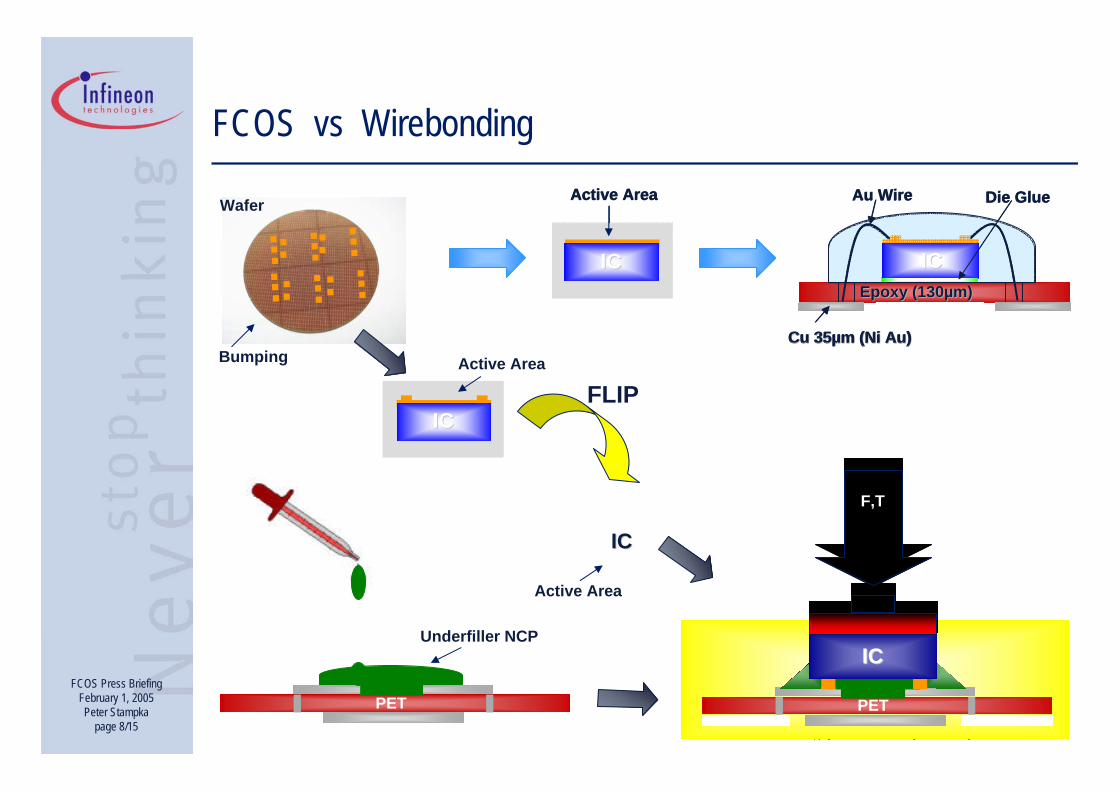
Fast transition from Wirebond to Flip Chip on Substrate (FCOS) technology

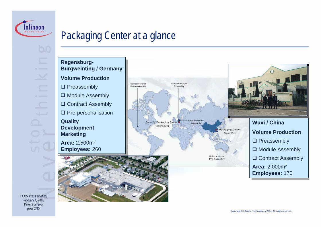
Leadsite Regensburg-Burgweinting with integratedmarketing/development/quality/production function

In time ramp of new technologies: ultrathin wafer, NiAu, bumping, Face-to-Face, powder antenna, etc.

Use synergies with central IC & Packaging Development

Integrated development with SEC business unit of newopportunities, such as personalization, contactless sub-systems(Epassport pre-lam, RFID inlay), etc.

Copyright © Infineon Technologies 2004. All rights reserved.

FCOS Press BriefingFebruary 1, 2005Peter Stampka

page 6/15

…already thinking of future requirements

MFC3.1 MFC5.6/8

Face-to-Faceearly prod. line

S-PackDBG

ultra thin

chip

MFCC8eD1 ePassport Inlays

Copyright © Infineon Technologies 2004. All rights reserved.

FCOS Press BriefingFebruary 1, 2005Peter Stampka

page 7/15

Why FCOSTM ?

2 tape suppliers dominated the chip card market

Cost of tapes more than 50% of total package costs

High price pressure due to overcapacity of module manufacturerswhich tape supplier did not follow

Increased mechanical and reliability requirements from the market

Enable new source of tape supplier (high volume)

Change to cheaper material cost of tape

Adapt process of module assembly to new tape

Work closely with card manufacturers for integration of new module technology into card

Solution

Market Situation before FCOS

Copyright © Infineon Technologies 2004. All rights reserved.

FCOS Press BriefingFebruary 1, 2005Peter Stampka

page 8/15

Cu 35Cu 35µµm (Ni Au)m (Ni Au)

Au Wire Die Glue

EpoxyEpoxy (130(130µµm)m)

ICIC

Cu 35Cu 35µµm (Ni Au)m (Ni Au)

Au Wire Die Glue

EpoxyEpoxy (130(130µµm)m)

ICICICIC

Active Area

ICIC

Active Area

PET

FLIPICIC

Active AreaBumping

Underfiller NCP

ICIC

Active Area

PET

ICICICIC

F,TF,T

Wafer

F,T

FCOS vs Wirebonding

Copyright © Infineon Technologies 2004. All rights reserved.

FCOS Press BriefingFebruary 1, 2005Peter Stampka

page 9/15

FCOS - Benefits

Increased temperature cycling by 10

Improvement for high dynamic bending stress (mailing)

Increased mechanical reliability for static tests

High corrosion resistance

Housing for large IC area

Increased implanting area

Green Package

FIPS (Federal Information Processing Standard) compatibility

Copyright © Infineon Technologies 2004. All rights reserved.

FCOS Press BriefingFebruary 1, 2005Peter Stampka

page 10/15

Max. IC-area: Wirebond vs. FCOS 6-contacts

Wirebond 6-contact module FCOS 6-contact module

Max. IC-area:1.9 x 1.9 mm

Max. IC-area:5.0 x 6.0 mm

Copyright © Infineon Technologies 2004. All rights reserved.

FCOS Press BriefingFebruary 1, 2005Peter Stampka

page 11/15

3rd Form Factor

- Punching tool of 6-contact at cardmanufacturer available

- Max. IC-area: ~30mm2

- For GSM application E2 until …mm2

(IFX) will fit in MFC5.6

First Form Factor(size of a credit card)

Second Form Factor(size of a SIM card, current norm forGSM devices)

Third Form Factor (3FF)Mini-UICC, half the size of the existing SIM card for use in high-end ultra-slim mobile phones and small devices such as GSM modems, WLAN cards - allows the design of small terminals

(e.g. data transmission only)- full backwards compatibility- implementation within a short time

frame, main production equipment usable

- can be punched out of the existing plug-in, all three form factors on one card possible

Copyright © Infineon Technologies 2004. All rights reserved.

FCOS Press BriefingFebruary 1, 2005Peter Stampka

page 12/15

FCOS - Ramp

FCOS vs Wirebond technology

0%10%20%30%40%50%60%70%80%90%

100%

04/05 05/06 06/07 07/08 08/09

FCOSWirebond

Copyright © Infineon Technologies 2004. All rights reserved.

FCOS Press BriefingFebruary 1, 2005Peter Stampka

page 13/15

Successful co-operation: Infineon and G&D

JOINT DEVELOPMENT with technology leading card manufacturer results in innovative product

Special CUSTOMER REQUIREMENTS have been incorporated into product definition to optimize the usage of the technology‘s advantages

TIME TO MARKETThe project development could be finalized efficiently because of the close cooperation and communication between Infineon and G&D as well as tape suppliers (simultaneous engineering)

FIRST TIME RIGHTSuccessful field trial of the new technology right after qualification


Recommended