FPGA Implementation of a Clockless
Stochastic LDPC Decoder
by
Christopher Ceroici
A thesis
presented to the University of Waterloo
in fulfillment of the
thesis requirement for the degree of
Master of Applied Science
in
Electrical and Computer Engineering
Waterloo, Ontario, Canada, 2014
© Christopher Ceroici, 2014
ii
I hereby declare that I am the sole author of this thesis. This is a true copy
of the thesis, including any required final revisions, as accepted by my
examiners. I understand that my thesis may be made electronically
available to the public.
iii
Abstract
This thesis presents a clockless stochastic low-density parity-check (LDPC)
decoder implemented on a Field-Programmable Gate Array (FPGA).
Stochastic computing reduces the wiring complexity necessary for
decoding by replacing operations such as multiplication and division with
simple logic gates. Clockless decoding increases the throughput of the
decoder by eliminating the requirement for node signals to be synchronized
after each decoding cycle. With this partial-update algorithm the decoder’s
speed is limited by the average wire delay of the interleaver rather than the
worst-case delay. This type of decoder has been simulated in the past but
not implemented on silicon. The design is implemented on an ALTERA
Stratix IV EP4SGX230 FPGA and the frame error rate (FER) performance,
throughput and power consumption are presented for (96,48) and (204,102)
decoders.
iv
Acknowledgements
I would first like to thank my supervisor Dr. Vincent Gaudet for his
guidance in this project.
I would also like to thank Brendan Crowley, Navid Bahrani and
Manpreet Singh for their assistance with HDL and FPGA operation.
Thank you to the Natural Sciences and Engineering Research
Council for funding and to ALTERA for donating the FPGA board.
v
Dedication
This thesis is dedicated to my family for their support which made this
possible.
vi
Table of Contents
List of Figures .................................................................................................................... viii
List of Tables ........................................................................................................................ x
Nomenclature ...................................................................................................................... xi
1 Introduction ....................................................................................................................... 1
1.1 Background ................................................................................................................... 1
1.2 Motivation ..................................................................................................................... 3
1.3 Thesis Organization ....................................................................................................... 4
2 Background........................................................................................................................ 6
2.1 Low-Density Parity-Check Codes ................................................................................. 6
2.2 Decoding using the SPA ................................................................................................ 8
2.3 Stochastic Decoding .................................................................................................... 13
2.4 Edge Memories............................................................................................................ 17
2.5 Noise-Dependent Scaling ............................................................................................ 18
2.6 Clockless Decoding ..................................................................................................... 19
3 FPGA Implementation ................................................................................................... 24
3.1 Overview ..................................................................................................................... 24
3.2 AWGN Generator........................................................................................................ 28
3.3 Random Number Generator ........................................................................................ 31
vii
3.4 Stochastic Stream Generator ....................................................................................... 33
3.5 Controller .................................................................................................................... 34
3.6 Variable Nodes ............................................................................................................ 35
3.7 Parity-Check Nodes ..................................................................................................... 38
4 Results and Discussion .................................................................................................... 42
4.1 Logic Utilization.......................................................................................................... 42
4.2 Frame Error Rate ......................................................................................................... 47
4.3 Throughput .................................................................................................................. 50
4.4 Power Measurements .................................................................................................. 52
5 Conclusion........................................................................................................................ 55
References ........................................................................................................................... 55
viii
List of Figures
1.1 Block diagram of a communication system with channel coding. ......................................... 2
2.1 Example of a 16x8 parity-check matrix. ................................................................................ 7
2.2 Tanner graph representation of the (16,8) parity-check matrix from Figure 2.1. ................... 8
2.3 Numerical simulation of the frame error rate (FER) of the (16,8) parity-check matrix
shown in Figure 2.1. .......................................................................................................................... 13
2.4 Stochastic gates for multiplication (top) addition (middle) and division (bottom). The
output bits will approximate the calculated value with more accuracy as more bits are used. ......... 14
2.5 Simple circuit implementation of a 2-input stochastic variable node. ................................. 16
2.6 Simple circuit implementation of a 2-input parity-check node. ........................................... 16
2.7 Simple circuit implementation of a 2-input parity-check node. ........................................... 19
2.8 Simple Tanner graph demonstrating the effects of wire delays, shown in blue in
nanoseconds. ..................................................................................................................................... 21
2.9 Simulation of the parity-check node signals of the Tanner graph in Figure using both a
synchronous and clockless circuit. .................................................................................................... 22
3.1 Block diagram of the clockless stochastic LDPC decoder. .................................................. 27
3.2 Gaussian distributions generated from a Box-Muller numerical simulation, the proposed
Gaussian generation technique, and the scaled ideal probability distribution. . ................................ 30
3.3 Illustration of the seed rotating technique. Each block represents a set of seeds used by
LFSRs. Arrows represent which block of seeds is currently being used. ......................................... 32
ix
3.4 Comparator used for stochastic bit generation. The 8-bit inputs Pi and R are the channel
probabilities and a random number. .................................................................................................. 33
3.5 Circuit implementation of a 3-input clockless stochastic variable node using an edge
memory (EM). ................................................................................................................................... 37
3.6 Schematic of the edge memory (EM) used in the clockless stochastic variable node. ........ 38
3.7 Parity-check node circuit for a synchronous stochastic LDPC decoder. The red and blue
lines represent the paths from which input ‘A’ affects output ‘0’. .................................................... 39
3.8 Circuit implementation of a 6-input clockless stochastic parity-check node. ...................... 40
4.1 Chip layout of (96,48) decoder (left) and (204,102) decoder (right). .................................. 44
4.2 Distribution of interleaver wire delays of the (96,48) decoder. Delays were determined
by estimating the path delays of the synthesized design. .................................................................. 45
4.3 Distribution of interleaver wire delays of the (204,102) decoder. Delays were
determined by estimating the path delays of the synthesized design. .............................................. 46
4.4 Frame error rate (FER) measurements of the (96,48) clockless stochastic decoder
implemented on an FPGA. ................................................................................................................ 49
4.5 Frame error rate (FER) measurements of the (96,48) clockless stochastic decoder
implemented on an FPGA. Results are shown with noise-dependent scaling parameter a = 2.
Measurements are compared with a numerical decoding simulation. ............................................... 50
4.6 Coded throughput measurements of the (96,48) and (204,102) clockless stochastic
decoders implemented on an FPGA. ................................................................................................. 51
4.7 Power consumption of (96,48) and (204,102) decoders implemented on an FPGA. ........... 53
4.8 Energy-per-coded bit of (96,48) and (204,102) decoders implemented on an FPGA. .........54
x
List of Tables
3.1 Summary of the variable node behavior………………………………………….……...35
4.1 Summary of the logic utilization of the (96,48) and (204,102) stochastic clockless
decoders synthesized on a ALTERA Stratix IV EP4SGX230 FPGA……………………….….43
xi
Nomenclature
AWGN Additive White Gaussian Noise
BER Bit Error Rate
FER Frame Error Rate
GF Galois Field
H Parity-Check Matrix
LDPC Low-Density Parity-Check
LFSR Linear Feedback Shift Register
LLR Log Likelihood Ratio
LUT Lookup Table
PDF Probability Density Function
RN Random Number
SNR Signal-to-Noise Ratio
SPA Sum-Product Algorithm
Tcl Tool command language
1
Chapter 1
Introduction
1.1 Background
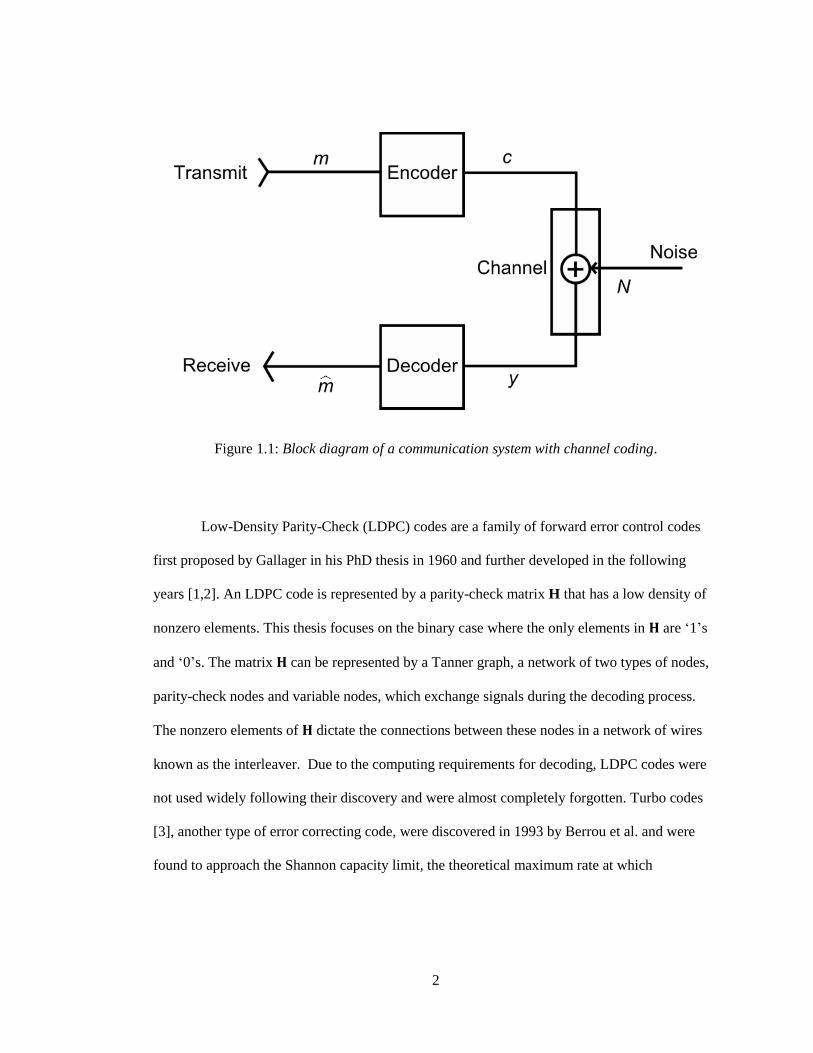
Channel coding is a technique used in digital communications to minimize the rate of errors
when messages are transmitted over a noisy channel. Figure 1.1 illustrates a high level view of
a baseband communication system where messages are encoded at the transmitter end and then
enter a channel where noise is superimposed on the encoded message. At the receiver end, the
decoder attempts to recover the initial message and minimize errors introduced by the noisy
channel. Channel coding is done by adding controlled redundant parity-check symbols to a
signal prior to transmission, allowing the decoder to reconstruct the original message with high
reliability at the receiver end.
2
Figure 1.1: Block diagram of a communication system with channel coding.
Low-Density Parity-Check (LDPC) codes are a family of forward error control codes
first proposed by Gallager in his PhD thesis in 1960 and further developed in the following
years [1,2]. An LDPC code is represented by a parity-check matrix H that has a low density of
nonzero elements. This thesis focuses on the binary case where the only elements in 𝐇 are ‘1’s
and ‘0’s. The matrix 𝐇 can be represented by a Tanner graph, a network of two types of nodes,
parity-check nodes and variable nodes, which exchange signals during the decoding process.
The nonzero elements of 𝐇 dictate the connections between these nodes in a network of wires
known as the interleaver. Due to the computing requirements for decoding, LDPC codes were
not used widely following their discovery and were almost completely forgotten. Turbo codes
[3], another type of error correcting code, were discovered in 1993 by Berrou et al. and were
found to approach the Shannon capacity limit, the theoretical maximum rate at which
3
information can be transmitted over a noisy communications channel. In 1997, LDPC codes
were rediscovered by MacKay et al. [4] and through the use of a probabilistic decoder rivaled
the performance of Turbo codes [4,5]. Following this discovery, the field of LDPC codes has
grown substantially.
The Sum-Product Algorithm (SPA) is an iterative decoding process which
approximates a maximum likelihood decoder but it more suitable for circuit implementations
[6-10]. Due to the many multiplication and division operations in the SPA, LDPC decoders
usually operate in the logarithmic domain which converts these multiplication operations into
summations. The SPA has a high degree of parallelism, so to maximize throughput in high-
speed applications, parallel LDPC decoder implementations are common [11].
1.2 Motivation
Stochastic computing is a method of random numerical computation first proposed in 1953 by
von Neumann [40]. Stochastic computing utilizes uncertainties and probabilities to perform
useful calculations. Continuous values can be represented by streams of random bits which
often results in lower complexity circuits. A decoding method which relies of the principles of
stochastic computing was proposed by Gaudet et al. in [41] as an alternative to the SPA. This
type of decoder benefits from lower complexity of the interleaver, however due to the serial
nature of stochastic computing, the calculations within individual nodes must be done serially,
reducing the throughput. To offset this deficiency, higher clock frequencies are often used.
However, a large high-speed clock network results in high power dissipation due to the high
4
switching activity of the clock. Furthermore, longer wires are required to meet the challenges of
the routing constraints of the LDPC interleaver, limiting the clock speed and hence the
throughput. Various techniques have been proposed to circumvent this problem such as
asynchronous decoding [12,13] and clockless decoding [14,15].
In a clockless decoder, the communication across the interleaver is restricted only by
the wiring delay. Furthermore, the decoding process no longer waits for all node calculations to
be completed before beginning the next decoding cycle. Since the wire delays will vary across
the interleaver in this continuous decoding technique, the decoding speed is limited by the
average of the wire delays rather than the largest wire delay. This type of decoder has been
demonstrated in high-level simulations in [14].
This thesis presents a Field-Programmable Gate Array (FPGA) implementation of a
clockless stochastic LDPC decoder and corresponding performance measurements. This work
demonstrates the feasibility for a practical clockless stochastic decoder.
1.3 Thesis Organization
This thesis is organized as follows: Chapter 2 reviews the sum-product algorithm (SPA) as well
as LDPC codes, stochastic decoders, and their synchronous, asynchronous and clockless
implementations. Chapter 3 presents the design of a clockless stochastic LDPC decoder with
details of individual components. Chapter 4 reports the frame error rate, throughput, and power
performance of the decoder and discusses some trade-offs between them. The FPGA logic
5
utilization is also discussed in this chapter. Chapter 5 discusses possible future work and
applications of this decoder and concludes the thesis.
6
Chapter 2
Background
This chapter summarizes the concepts of LDPC codes, Tanner graphs and the sum product
algorithm in Sections 2.1 and 2.2. Stochastic decoding is introduced in section 2.3 while
sections 2.4 and 2.5 present the concepts of noise-dependent scaling and edge memories.
Section 2.6 summarizes clockless stochastic decoding of LDPC codes and its benefits.
2.1 Low-Density Parity-Check Codes
Discovered in the early 1960s [1,2], LDPC codes are a class of linear block codes with a sparse
parity-check matrix, 𝑯 of size (𝑛 − 𝑘) by 𝑛 [37,38]. LDPC codes can be defined for any order
of Galois field but this thesis will focus on LDPC codes over GF(2). The length of the message
is k symbols (usually bits) while the encoded message is of length n. LDPC codes have a code
rate of 𝑅 = 𝑘/𝑛 which represents the ratio of message bits to codeword bits. A binary vector 𝒄
is a codeword if 𝒄𝑯𝑻 = 𝟎. In other words, a codeword must be orthogonal to every row of 𝑯.
There also exists a generator matrix 𝑮 consisting of the basis vectors of the decoder and from
7
which 𝑮𝑯𝑻 = 𝟎. The generator matrix can be used to encode messages and is defined in terms
of 𝑯 from the expressions 𝑯 = [−𝑷𝑻|𝑰𝒏−𝒌] and 𝑮 = [𝑰𝒌|𝑷].
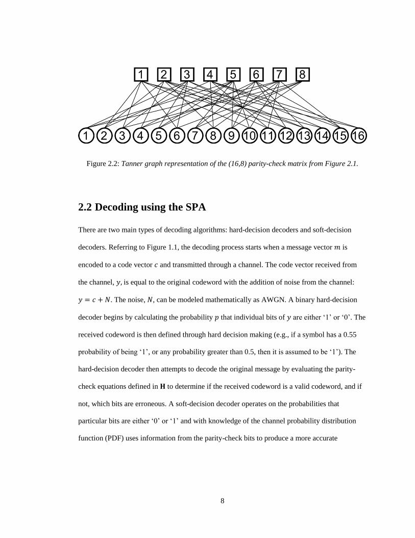
An LDPC code can also be displayed graphically as a bipartite Tanner Graph [16].
Within a Tanner Graph there exists two types of nodes: variable nodes (shown as circles) and
parity-check nodes (shown as squares). A line connecting a variable node to a parity-check node
is represented by a ‘1’ in 𝑯. The variable nodes each represent a single codeword bit while each
parity-check node represents a single parity-check equation. A line connecting a variable node
to a parity-check node suggests that this bit is included in that particular parity-check equation.
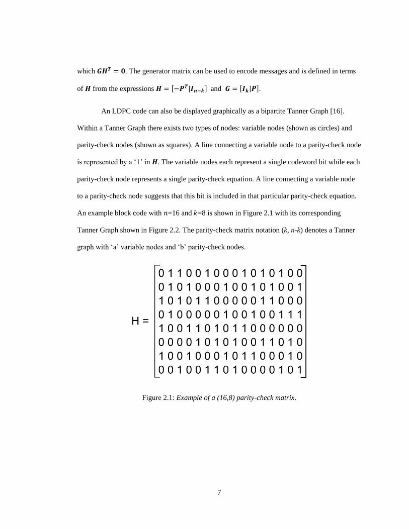
An example block code with 𝑛=16 and 𝑘=8 is shown in Figure 2.1 with its corresponding
Tanner Graph shown in Figure 2.2. The parity-check matrix notation (k, n-k) denotes a Tanner
graph with ‘a’ variable nodes and ‘b’ parity-check nodes.
Figure 2.1: Example of a (16,8) parity-check matrix.
8
Figure 2.2: Tanner graph representation of the (16,8) parity-check matrix from Figure 2.1.
2.2 Decoding using the SPA
There are two main types of decoding algorithms: hard-decision decoders and soft-decision
decoders. Referring to Figure 1.1, the decoding process starts when a message vector 𝑚 is
encoded to a code vector 𝑐 and transmitted through a channel. The code vector received from
the channel, 𝑦, is equal to the original codeword with the addition of noise from the channel:
𝑦 = 𝑐 + 𝑁. The noise, 𝑁, can be modeled mathematically as AWGN. A binary hard-decision
decoder begins by calculating the probability 𝑝 that individual bits of 𝑦 are either ‘1’ or ‘0’. The
received codeword is then defined through hard decision making (e.g., if a symbol has a 0.55
probability of being ‘1’, or any probability greater than 0.5, then it is assumed to be ‘1’). The
hard-decision decoder then attempts to decode the original message by evaluating the parity-
check equations defined in 𝐇 to determine if the received codeword is a valid codeword, and if
not, which bits are erroneous. A soft-decision decoder operates on the probabilities that
particular bits are either ‘0’ or ‘1’ and with knowledge of the channel probability distribution
function (PDF) uses information from the parity-check bits to produce a more accurate
9
estimation of the bit-value probabilities. In an iterative decoder, the hard decision bits can be
calculated after each iteration to check for a valid codeword, otherwise the decoder continues to
attempt to produce more accurate probabilities.
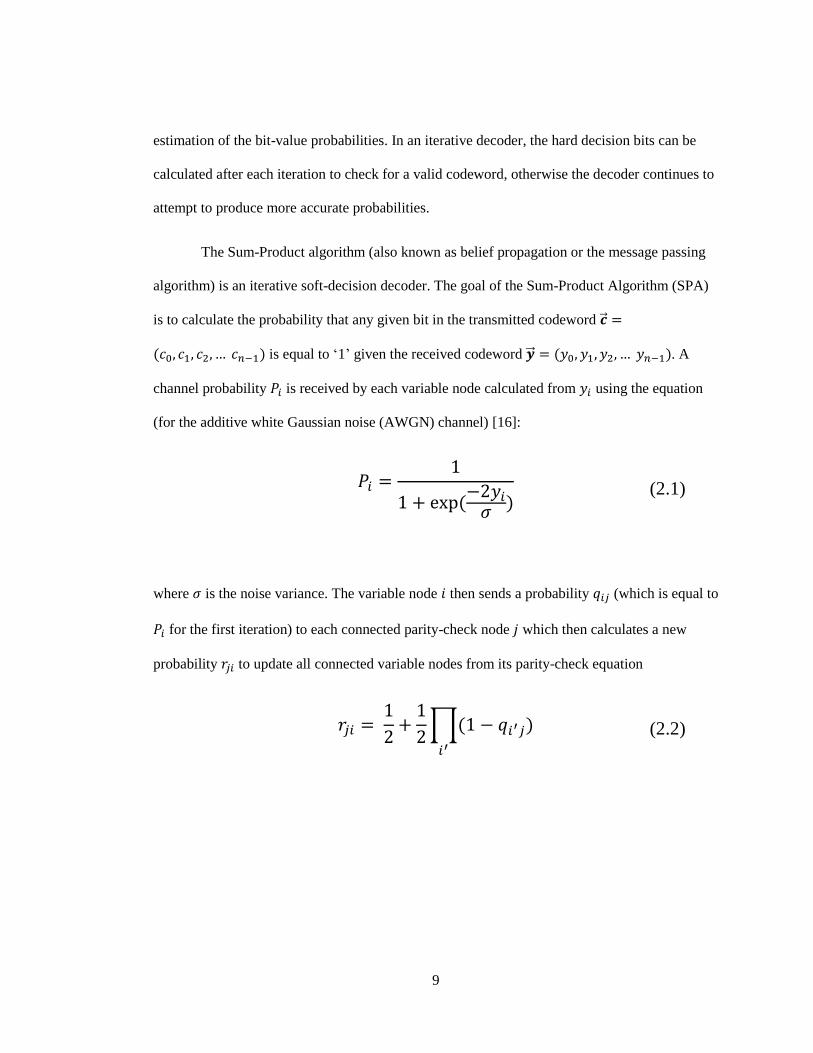
The Sum-Product algorithm (also known as belief propagation or the message passing
algorithm) is an iterative soft-decision decoder. The goal of the Sum-Product Algorithm (SPA)
is to calculate the probability that any given bit in the transmitted codeword =
(𝑐0, 𝑐1, 𝑐2, … 𝑐𝑛−1) is equal to ‘1’ given the received codeword = (𝑦0, 𝑦1, 𝑦2, … 𝑦𝑛−1). A
channel probability 𝑃𝑖 is received by each variable node calculated from 𝑦𝑖 using the equation
(for the additive white Gaussian noise (AWGN) channel) [16]:
𝑃𝑖 =
1
1 + exp (−2𝑦𝑖
𝜎) (2.1)
where 𝜎 is the noise variance. The variable node 𝑖 then sends a probability 𝑞𝑖𝑗 (which is equal to
𝑃𝑖 for the first iteration) to each connected parity-check node 𝑗 which then calculates a new
probability 𝑟𝑗𝑖 to update all connected variable nodes from its parity-check equation
𝑟𝑗𝑖 = 1
2+
1
2∏(1 − 𝑞𝑖′𝑗)
𝑖′
(2.2)
10
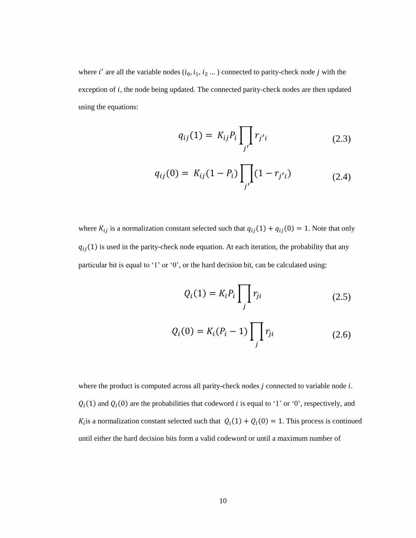
where 𝑖′ are all the variable nodes (𝑖0, 𝑖1, 𝑖2 … ) connected to parity-check node 𝑗 with the
exception of 𝑖, the node being updated. The connected parity-check nodes are then updated
using the equations:
𝑞𝑖𝑗(1) = 𝐾𝑖𝑗𝑃𝑖 ∏𝑟𝑗′𝑖
𝑗′
(2.3)
𝑞𝑖𝑗(0) = 𝐾𝑖𝑗(1 − 𝑃𝑖)∏(1 − 𝑟𝑗′𝑖
𝑗′
) (2.4)
where 𝐾𝑖𝑗 is a normalization constant selected such that 𝑞𝑖𝑗(1) + 𝑞𝑖𝑗(0) = 1. Note that only
𝑞𝑖𝑗(1) is used in the parity-check node equation. At each iteration, the probability that any
particular bit is equal to ‘1’ or ‘0’, or the hard decision bit, can be calculated using:
𝑄𝑖(1) = 𝐾𝑖𝑃𝑖 ∏𝑟𝑗𝑖
𝑗
(2.5)
𝑄𝑖(0) = 𝐾𝑖(𝑃𝑖 − 1)∏𝑟𝑗𝑖𝑗
(2.6)
where the product is computed across all parity-check nodes 𝑗 connected to variable node 𝑖.
𝑄𝑖(1) and 𝑄𝑖(0) are the probabilities that codeword 𝑖 is equal to ‘1’ or ‘0’, respectively, and
𝐾𝑖is a normalization constant selected such that 𝑄𝑖(1) + 𝑄𝑖(0) = 1. This process is continued
until either the hard decision bits form a valid codeword or until a maximum number of
11
iterations has been completed. If the decoder reaches the maximum number of iterations an
error is declared and the bit error rate can be computed by comparing the hard decision bits with
the original codeword.
The SPA involves many multiplication and division operations for both node
computations and for the normalization conditions of the variable nodes. Therefore, a hardware
implementation of such a decoder would be extremely area inefficient as hardware multipliers
are much more complex than hardware adders. To bypass this problem, hardware SPA decoders
operate in the logarithm domain. Rather than calculating the channel probability 𝑃𝑖 initially, a
Log-Likelihood Ratio (LLR) 𝐿𝑖 = log (𝑃(𝑦𝑖=0)
𝑃(𝑦𝑖=1)) is calculated. For an AWGN channel, this is
calculated using the following equation.
𝐿𝑖 =2𝑦𝑖
𝜎2 (2.7)
The variable and parity-check node likelihood signals are then updated using the
following equations.
𝐿(𝑟𝑗𝑖) = [∏𝑠𝑖𝑔𝑛(𝐿(𝑞𝑖′𝑗))
𝑖′
] · 𝜙 (∑𝜙(|𝐿(𝑞𝑖′𝑗)|
𝑖′
)) (2.8)
𝜙(𝑥) = log (𝑒𝑥 + 1
𝑒𝑥 − 1) (2.9)
𝐿(𝑞𝑖𝑗) = 𝐿𝑖 + ∑𝐿(𝑟𝑗′𝑖)
𝑗′
(2.10)
12
𝐿(𝑟𝑗𝑖) is the log-likelihood ratio signal sent from parity-check nodes to variable
nodes and 𝐿(𝑞𝑖𝑗) is the ratio sent from variable to parity-check nodes. The hard decision
bits can be calculated using:
𝐿(𝑄𝑖𝑗) = 𝐿𝑖 + ∑𝐿(𝑟𝑗𝑖)
𝑗
(2.11)
Where bit 𝑖 is equal to ‘1’ if 𝐿(𝑄𝑖𝑗) < 0 and is equal to ‘0’ otherwise. This is the same
equation used for calculating 𝐿(𝑞𝑖𝑗) except signals from all of the connected nodes are
considered. The log-domain SPA can be implemented in a circuit much more efficiently than
the SPA since the multiplication operations have been reduced to summation operations. The
calculation of 𝜙(𝑥) can be done using a look-up table (LUT) efficiently since it is an even
function [42]. An additional LUT is required for the initial logarithm transformation of the
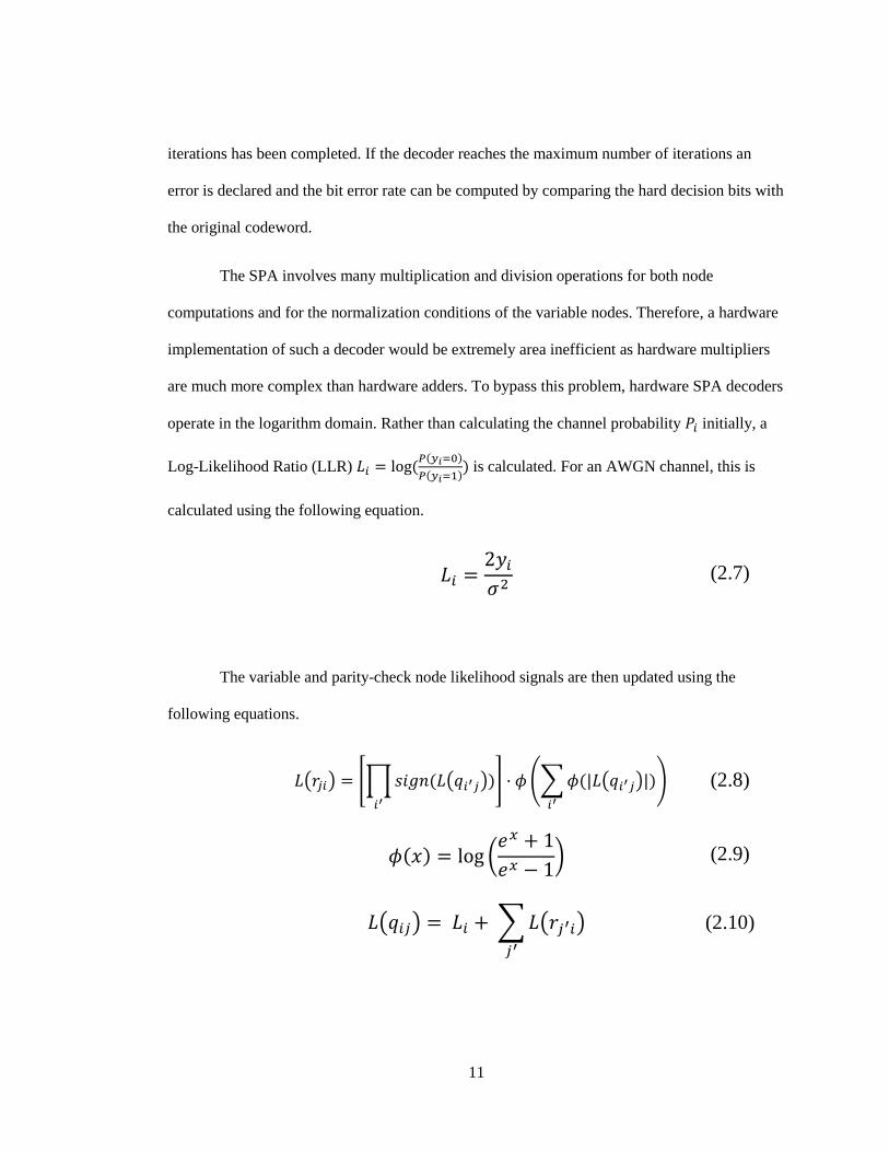
received channel probability. A simulation of the block code from Figure 2.1 is shown in
Figure 2.3 using the log-domain SPA Equations 2.7 to 2.11. Note that this decoder is used as a
demonstration and a practical LDPC decoder would use a much larger code resulting in much
better performance. Figure 2.3 shows the frame error rate (FER), or the fraction of errors that
were detected at varying signal-to-noise ratios (SNRs) through an entire decoding process after
repeating the simulation many times until a significant number of errors have been detected.
This simulation was calculated using AWGN applied to zero-value codewords.
13
Figure 2.3: Numerical simulation of the frame error rate (FER) of the (16,8) parity-check
matrix shown in Figure 2.1.
2.3 Stochastic Decoding
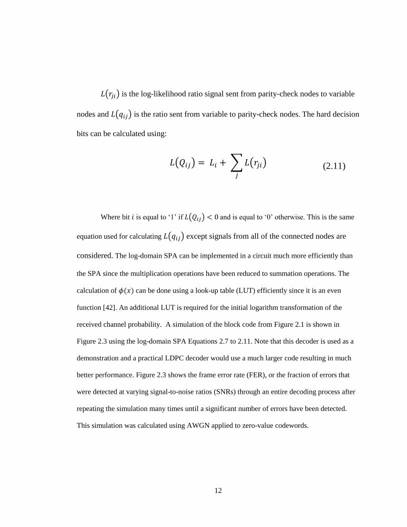
Stochastic computing is the process of using randomness to achieve useful computation.
Continuous value signals can be represented by a stream of randomly generated bits where the
values are communicated from the statistical means of the bit streams. The probability of
14
stochastic stream is equal to the ratio of ‘1’s to ‘0’s and so there are many possible
representations of any probability. For example the probability 0.6 can be represented by the
streams 10110 or 0110101011. The order in which the ‘1’s appear in the stochastic sequence is
not important.
Figure 2.4: Stochastic gates for multiplication (top) soft XOR (middle) and division (bottom).
The output bits will approximate the calculated value with more accuracy as more bits are used.
15
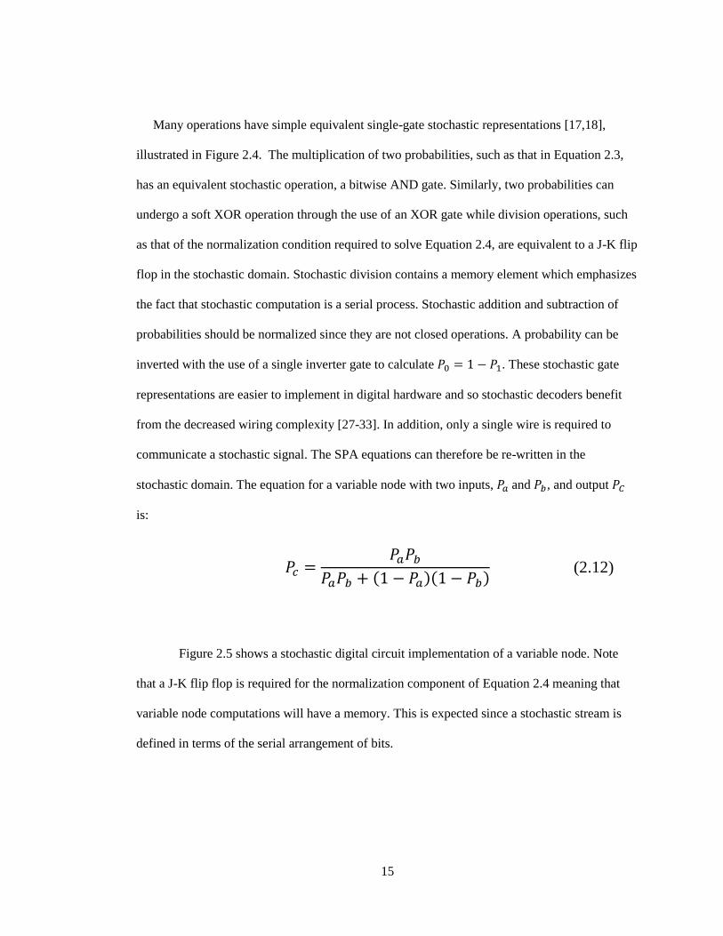
Many operations have simple equivalent single-gate stochastic representations [17,18],
illustrated in Figure 2.4. The multiplication of two probabilities, such as that in Equation 2.3,
has an equivalent stochastic operation, a bitwise AND gate. Similarly, two probabilities can
undergo a soft XOR operation through the use of an XOR gate while division operations, such
as that of the normalization condition required to solve Equation 2.4, are equivalent to a J-K flip
flop in the stochastic domain. Stochastic division contains a memory element which emphasizes
the fact that stochastic computation is a serial process. Stochastic addition and subtraction of
probabilities should be normalized since they are not closed operations. A probability can be
inverted with the use of a single inverter gate to calculate 𝑃0 = 1 − 𝑃1. These stochastic gate
representations are easier to implement in digital hardware and so stochastic decoders benefit
from the decreased wiring complexity [27-33]. In addition, only a single wire is required to
communicate a stochastic signal. The SPA equations can therefore be re-written in the
stochastic domain. The equation for a variable node with two inputs, 𝑃𝑎 and 𝑃𝑏, and output 𝑃𝐶
is:
𝑃𝑐 =𝑃𝑎𝑃𝑏
𝑃𝑎𝑃𝑏 + (1 − 𝑃𝑎)(1 − 𝑃𝑏) (2.12)
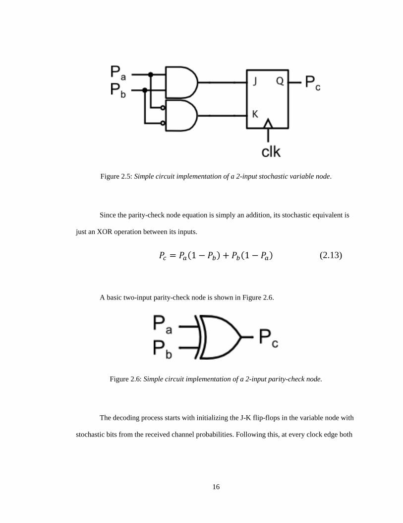
Figure 2.5 shows a stochastic digital circuit implementation of a variable node. Note
that a J-K flip flop is required for the normalization component of Equation 2.4 meaning that
variable node computations will have a memory. This is expected since a stochastic stream is
defined in terms of the serial arrangement of bits.
16
Figure 2.5: Simple circuit implementation of a 2-input stochastic variable node.
Since the parity-check node equation is simply an addition, its stochastic equivalent is
just an XOR operation between its inputs.
𝑃𝑐 = 𝑃𝑎(1 − 𝑃𝑏) + 𝑃𝑏(1 − 𝑃𝑎) (2.13)
A basic two-input parity-check node is shown in Figure 2.6.
Figure 2.6: Simple circuit implementation of a 2-input parity-check node.
The decoding process starts with initializing the J-K flip-flops in the variable node with
stochastic bits from the received channel probabilities. Following this, at every clock edge both
17
sets of nodes are updated with signals from their connected nodes. The decoding process
continues until either a valid codeword is found, identified by the parity-check equations at the
parity-check nodes being satisfied, or until a pre-defined number of clock cycles has completed
at which point an error is declared and the next frame begins.
2.4 Edge Memories
The variable node circuit shown in Figure 2.5 is not ideal since it can result in locked states
during the decoding process. Locked states are cases where the output of the node remains the
same over several decoding cycles. This lack of switching activity can slow the convergence of
the decoder. Tanner graphs with cycles are particularly susceptible to this phenomenon. A cycle
can result in a particular group of nodes becoming locked in a fixed state [33]
To circumvent this problem edge memories (EMs) were proposed by Tehrani et al. in
[31]. EMs are memory elements, usually shift registers, which are used instead of J-K flip-flops
and update their values based on the inputs of the variable node. The purpose of EMs is to re-
randomize stochastic streams so that consecutive bits are independent of each other. The output
bit of the variable node can be classified as either regenerative or degenerative. A regenerative
bit is the case where the inputs to a variable node are equal. A degenerative bit is produced
when the node inputs are not equal. If the variable node produces a regenerative bit it is used as
the output of the node and also stored in the EM. When a degenerative bit is produced it is
ignored and the output of the variable node is instead selected from the EM at a random address.
This mechanism prevents the decoder from becoming stuck in a “lock” state where there is no
18
switching activity at a variable node for a period of time. The EM must also have a forgetting
mechanism where new regenerative bits replace old ones. EMs are usually preloaded with bits
from the channel probability prior to decoding. Decoding can also begin with the EMs
initialized to a zero state at the cost of slower decoder convergence.
2.5 Noise-Dependent Scaling
As the SNR changes, so will the amount of switching activity. This is because the channel
probabilities will not use the full scale. Less switching activity results in slower convergence
and poorer FER performance. Noise-dependent scaling (NDS) is a method of ensuring a
constant amount of switching activity across different SNRs [31]. This is done by scaling the
received LLRs by a parameter proportional to the SNR. The scaled LLR 𝐿𝑖′ is calculated using:
𝐿𝑖′ = (
2𝛼𝜎2
𝑌)𝐿𝑖 =
4𝛼𝑦𝑖
𝑌 (2.14)
where 𝐿𝑖 is the LLR calculated using Equation 2.7. The parameter 𝛼 is chosen experimentally
for best performance. 𝑌 is set to be the maximum expected unscaled LLR value, usually set to
𝑌 = 6. Notice that the 𝜎 cancels in the above equation. This suggests that the noise power will
have no effect on the magnitude of 𝐿𝑖′ and therefore the switching activity. However, in a
practical decoder the LLR value 𝐿𝑖 is usually the decoder input so a channel noise measurement
will still be required to obtain 𝜎. This scaling operation is usually done using a LUT.
19
2.6 Clockless Decoding
Two alternatives to synchronous decoding are asynchronous decoding and clockless decoding
[12-15]. Asynchronous decoding eliminates the global clock and instead uses a handshaking
mechanism for nodes to communicate across the interleaver. Using these request-acknowledge
signals rather than a large clock network, as illustrated in Figure 2.7, eliminates the problem of
varying clock delays across different nodes. This increases the overall throughput as well as
reduces power consumption. However the introduction of request-acknowledge signals does
incur a cost as there is an increase in the size and wiring complexity of the interleaver.
Figure 2.7: Simple circuit implementation of a 2-input parity-check node.
When a parity-check node finishes its calculation it must wait for every other parity-
check node to complete as well before updating the variable nodes. Since the wiring delay
between different nodes will vary, the speed of the decoder will be limited by the largest wire
delay in the interleaver.
20
If a node were to send its calculated bit immediately to its connected nodes rather than
waiting, some of the inputs of the connected nodes would be new while others would be
outdated. However, since stochastic computations depend on the time averages of binary signals
the intermediate bit produced by a node with outdated inputs doesn’t have a significant impact
on the overall decoding process. Ignoring this synchronization constraint eases the restrictions
on the decoder design and allows for the exploration of larger design spaces than previously
possible. Clockless decoding removes these two limitations by ignoring the synchronization
constraint amongst nodes. As soon as a node has completed its calculation it immediately sends
its output to the connected nodes. This partial-update algorithm, described in [19-21], allows for
the decoding speed to be determined by the average wire delay. A sample Tanner graph is
shown in Figure 2.8 with illustrated wire delays shown in blue in nanoseconds, for illustrative
purposes.
21
Figure 2.8: Simple Tanner graph demonstrating the effects of wire delays, shown in blue in
nanoseconds.
If a synchronous decoder were used for this graph the throughput would be restricted by
the largest wire delay, the delay between parity-check node 1 and variable node 0, while a
clockless decoder would not. This can be seen in Figure 2.9 which shows a simulated set of
communications between the nodes of Figure 2.8 for both a synchronous decoder and a
clockless decoder with their respective wire delays. The nodes in this simulation are the
simplest stochastic variable and parity-check node designs shown in Figures 2.5 and 2.6. Here,
the synchronous decoder uses the maximum clock frequency allowed by the wire delays.
22
Figure 2.9: Simulation of the parity-check node signals of the Tanner graph in Figure 2.8 using
both a synchronous and clockless circuit.
Comparing the first signal of parity-check node 0 (the connection from parity-check
node 0 to variable node 0) of the synchronous and clockless decoders in Figure 2.9, the
synchronous signal has a period of 31.5 ns while the clockless signal has a period of 14 ns. The
ratio of these periods, 2.25, is approximately equal to 2, the ratio of the largest wire delay to the
average wire delay. Because of the different wire delays the nodes of the clockless decoder will
often use outdated signals for its computations resulting in more switching activity. However,
23
these extra signals do not have a significant negative effect on the calculations or the speed of
convergence. A stochastic LDPC decoder using the partial-update scheduling algorithm was
simulated in [15] using 90 nm technology and resulted in a lower error floor, the flattening of
the error rate curve at high SNR, than a synchronous decoder. There has been no physical
demonstration of this type of decoder to date. The goal of this thesis is to demonstrate a proof-
of-concept design of a clockless stochastic LDPC decoder and to learn as much as possible from
this implementation.
24
Chapter 3
FPGA Implementation
This chapter describes the architecture of clockless stochastic LDPC decoder. Section 3.1
summarizes the overall design. Section 3.2 and 3.3 presents the designs of an AWGN generator
and the (pseudo) random number generators required for real-time testing of the decoder
hardware. Section 3.4 describes the comparator used for generating stochastic bits. The designs
of the variable and parity-check nodes are presented in Sections 3.6 and 3.7.
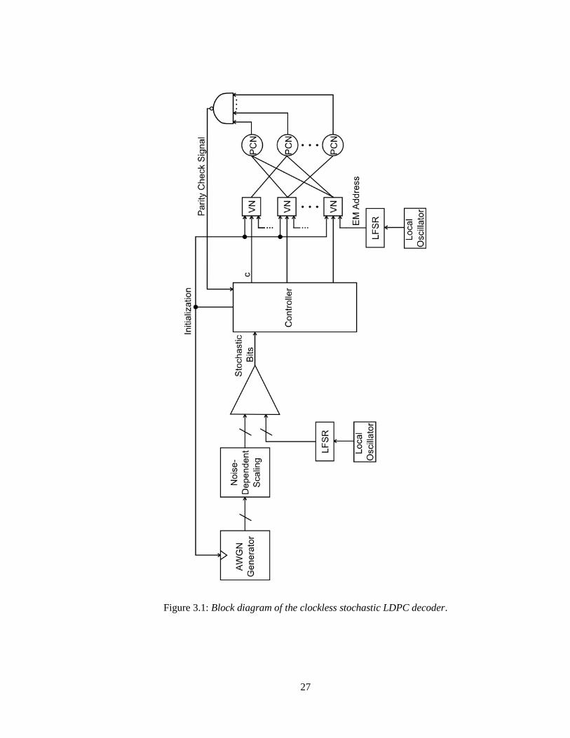
3.1 Overview
The clockless stochastic LDPC decoder was implemented on an ALTERA Stratix IV
EP4SGX230 FPGA using the Quartus II set of computer aided design tools [36]. The design
consists of the following modules:
An AWGN generator which (pseudo) randomly generates zero-codeword LLRs and
then scales them according to the noise power.
A comparator used for the conversion of LLRs into stochastic streams.
A controller to initialize the decoder and to begin and terminate frames.
25
The parity-check and variable nodes and the interleaver connecting them.
A block diagram of the decoder is shown in Figure 3.1. At each initialization phase
LLRs are generated and scaled. The LLRs are then converted into a stochastic stream using an
external or local clock. These stochastic bits are then passed on to the variable nodes for
decoding or preloading the EMs during initialization. This initialization phase could be skipped
by preloading the EMs with ‘0’s at the expense of the decoder’s speed of convergence.
However, since this decoder uses zero-value codewords for testing purposes the variable nodes
would begin decoding with a bias towards the correct codeword. The EMs in the variable nodes
use random addresses generated from LFSRs. The decoding process terminates when a valid
codeword is detected by the variable nodes or until the controller declares an error.
The Verilog hardware description files (HDL) for the interleaver as well as any other
modules dependent on 𝑯 are generated using a C++ script which reads in 𝑯 in alist format, an
efficient way of representing large, sparse binary matrices. 𝑯 is then converted into matrix form
where the ‘1’s indicate connections between the variable and parity-check nodes. This matrix is
then used to generate the HDL for the interleaver, the module where the variable and parity-
check node modules are instantiated and their connecting wires are assigned according to 𝑯.
The script also generates sets of (pseudo) random seeds to initialize the linear feedback shift
registers (LFSRs).
The 96x48 and 204x102 parity-check matrices used for the designs in this thesis
research were acquired from [22]. However, the script used here can generate HDL files for any
26
regular (3,6) LDPC code, or any code with a Tanner graph having parity-check nodes with six
connections and variable nodes with three connections.
27
Figure 3.1: Block diagram of the clockless stochastic LDPC decoder.
28
3.2 AWGN Generator
The decoder uses zero-value codewords with AWGN for testing purposes. The most common
method of generating AWGN on-chip is using the Box-Muller transformation, shown below
[23,24].
𝑌 = √−2ln (𝑥1) cos (2𝜋𝑥2) (3.1)
where 𝑥1 and 𝑥2 are two uniformly distributed random numbers and 𝑌 is a normally distributed
random number. To implement this algorithm in a digital circuit, two LUTs and a multiplier are
required. In addition, the square root operation is very non-linear and therefore the quantization
error of the LUTs will be large if the LUT uses linear indexing. To avoid this nonlinearity as
well as significantly reduce the area consumption of the AWGN generator, a new design is
proposed here.
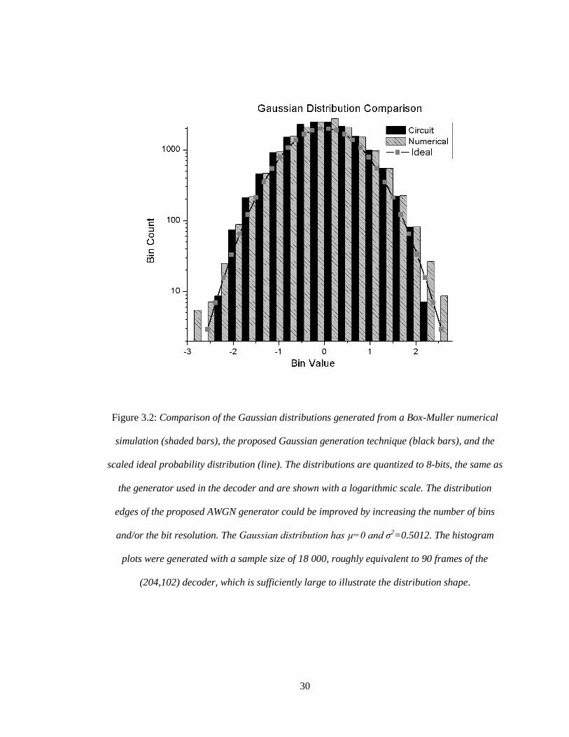
An AWGN distribution can be generated using a single LUT by dividing the LUT into
a set of bins with sizes calculated from the desired distribution. The Gaussian distribution is first
calculated across upper and lower bounds 𝑥𝑈 and 𝑥𝐿 which are calculated using the following
equation:
𝑥𝐿,𝑈 = µ ± 𝜎√−2ln (𝛽) (3.2)
where µ and 𝜎 are the mean and standard deviation of the AWGN distribution and 𝛽 is the ratio
of the probability at the outer bounds to the probability at the distribution center. In this design
𝛽 = 0.01 was used. The distribution is then divided into a number of bins. The bin counts are
29
normalized and then used to partition the LUT. For example, the bin with the highest count, the
peak of the distribution, will occupy the most space in the LUT. Therefore when a uniformly
distributed random bit, such as that generated from an LFSR, is used as an input it will have a
probability of falling on an address with the largest bin approximately equal to the probability
of the bin calculated from the distribution. A hardware simulation of this design generating a
Gaussian distribution with 𝜎 = 1 and zero mean is shown in Figure 3.2 compared with a
numerically generated distribution using the Box-Muller Algorithm and the ideal Gaussian
distribution calculated using MATLAB.
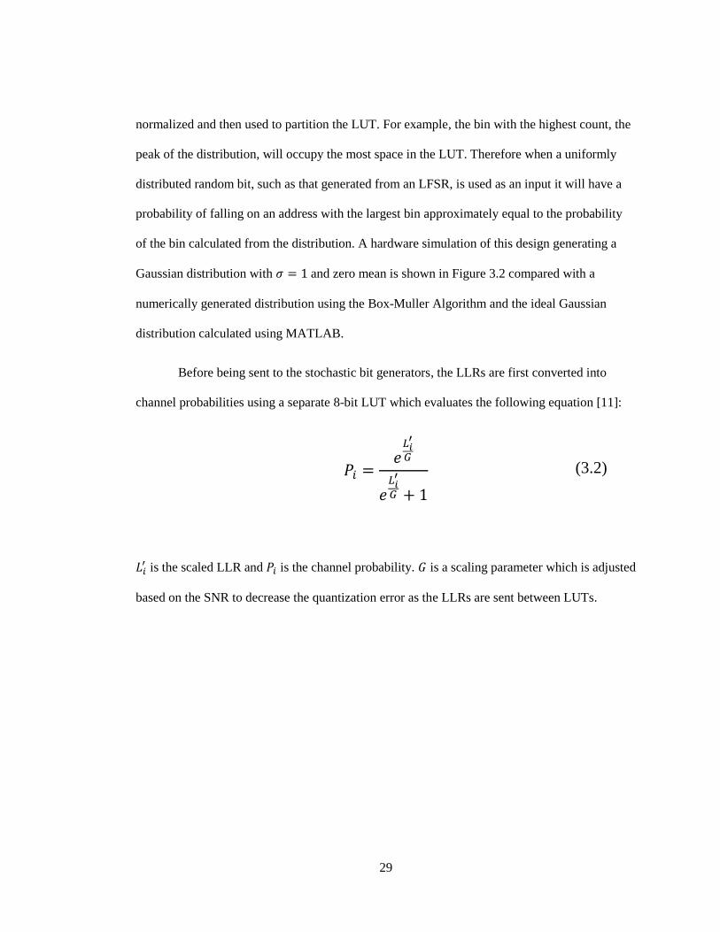
Before being sent to the stochastic bit generators, the LLRs are first converted into
channel probabilities using a separate 8-bit LUT which evaluates the following equation [11]:
𝑃𝑖 =𝑒
𝐿𝑖′
𝐺
𝑒𝐿𝑖′
𝐺 + 1
(3.2)
𝐿𝑖′ is the scaled LLR and 𝑃𝑖 is the channel probability. 𝐺 is a scaling parameter which is adjusted
based on the SNR to decrease the quantization error as the LLRs are sent between LUTs.
30
Figure 3.2: Comparison of the Gaussian distributions generated from a Box-Muller numerical
simulation (shaded bars), the proposed Gaussian generation technique (black bars), and the
scaled ideal probability distribution (line). The distributions are quantized to 8-bits, the same as
the generator used in the decoder and are shown with a logarithmic scale. The distribution
edges of the proposed AWGN generator could be improved by increasing the number of bins
and/or the bit resolution. The Gaussian distribution has µ=0 and σ2=0.5012. The histogram
plots were generated with a sample size of 18 000, roughly equivalent to 90 frames of the
(204,102) decoder, which is sufficiently large to illustrate the distribution shape.
31
3.3 Random Number Generator
Random numbers are used by the AWGN generator, the stochastic comparator, and the
generation of addresses for the EMs. These random numbers are generated using 16-bit LFSRs
[25,26]. The LFSRs are constructed using the primitive polynomial 𝑥16 + 𝑥5 + 𝑥3 + 𝑥2 + 1
which generates (216-1) 16-bit random numbers (RNs) before repeating the cycle. The choice of
a primitive polynomial configuration ensures that the LFSR produces a maximum length
sequence. These RNs are then split into two 8-bit RNs which are used by the AWGN generator
and the stochastic stream generators. Since the EMs are 8-bit registers they only require a 3-bit
address and so the 8-bit EM RNs are further divided. Also, different EMs will have different
stored bits and so the same address can be used for more than one EM. For a (96,48) code with
96 variable nodes and 288 EMs (each node has three outputs) only 96 random addresses are
used.
For high SNR testing where many frames are required, the decoder may need more than
(216-1) RNs in which case the RNs and the switching activity would repeat. To avoid this
problem, the LFSRs are reinitialized with new seeds when the decoder approaches (216-1) RNs.
If K sets of seeds are stored in the decoder, this allows for K(216-1) unique RNs. However, as K
increases, so does the FPGA logic utilization as well as the compilation time. To maximize the
number of unique frames, the seeds are divided into two groups each with size K/2. When all
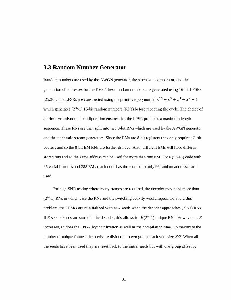
the seeds have been used they are reset back to the initial seeds but with one group offset by
32
one. Therefore, the two groups will go through every combination before repeating themselves
allowing for K2(216-1) unique RNs per LFSR. An illustration of this technique is shown in
Figure 3.3.
Figure 3.3: Illustration of the seed rotating technique. Each block represents a set of seeds used
by LFSRs. Arrows represent which block of seeds is currently being used.
The stochastic comparator and the EM address generators are used throughout the
decoding process while the AWGN generators are used only at the beginning of each frame.
Therefore it is not necessary to update the LFSR seeds used for the AWGN generators. If the
decoder exceeds (216-1) frames and the channel probabilities repeat, the LFSRs used to generate
stochastic bits and EM addresses will still be unique and so the switching activity of the decoder
will also be different. This reduces the size of the AWGN generator module.
33
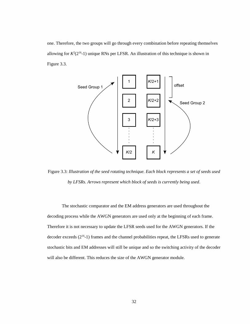
3.4 Stochastic Stream Generator
Stochastic bits are generated using a comparator, shown in Figure 3.4, with two inputs: the 8-bit
channel probability and an 8-bit random number generated from a LFSR. If the channel
probability is larger than the random number a ‘1’ is generated, otherwise the output is ‘0’. The
LFSR is triggered by a local oscillator such as a ring oscillator. The LFSR could also be
triggered by a global clock since clock delays will not impact the decoder performance due to
the partial-update algorithm.
Figure 3.4: Comparator used for stochastic bit generation. The 8-bit inputs Pi and R are the
channel probabilities and a random number.
34
3.5 Controller
The controller routes stochastic bits from the comparators to the interleaver and controls the
rotation of seeds for the (pseudo) random number generators. The controller also toggles the
decoder between two main states:
Initialization phase: During the initialization phase, the stochastic bits are fed directly
into the EMs of the variable nodes, bypassing the node equations. During initialization,
the signals between nodes are suppressed. The beginning of the initialization phase also
triggers the AWGN generator to produce a new set of noise signal inputs. After a
certain number of initialization phases have passed, the controller instructs the seed
module to rotate to a new set and for the LFSRs to be reinitialized. Depending on the
speed of stochastic bit generation, the initialization phase continues for as long as it
takes to fill the EMs with channel probabilities.
Decoding phase: Immediately after the EMs have been preloaded, the controller
disables the initialization signal and the connection from the stochastic stream directly
to the EMs is severed. The channel probabilities are instead set as inputs to the variable
nodes. The connections between variable and parity-check nodes are allowed to
communicate freely, limited only by their gate and wire delays. During the decoding
phase the controller checks for the parity-check equations of each parity-check node to
be satisfied simultaneously. When this occurs, a valid codeword has been found by the
decoder and the initialization phase begins for the next decoding frame. While
decoding the controller also increments a counter using the on-board 50MHz clock.
When the counter reaches the predefined value 300, an error is declared and the next
35
frame is initialized. The value of this counting limit duration is chosen based on the
desired performance trade-off between throughput and FER.
3.6 Variable Nodes
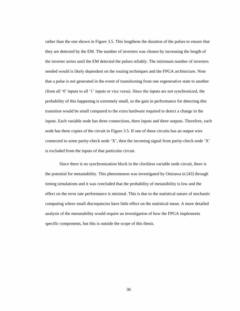
The 3-input continuous time variable node circuit is shown in Figure 3.5. This circuit was
proposed in [15]. Signal ‘U’ determines whether the node is in a regenerative state (all inputs
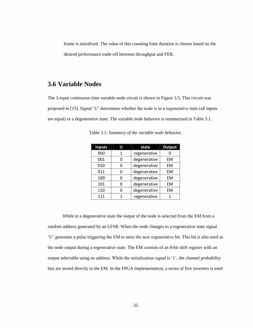
are equal) or a degenerative state. The variable node behavior is summarized in Table 3.1.
Table 3.1: Summary of the variable node behavior.
Inputs U state Output
000 1 regenerative 0
001 0 degenerative EM
010 0 degenerative EM
011 0 degenerative EM
100 0 degenerative EM
101 0 degenerative EM
110 0 degenerative EM
111 1 regenerative 1
While in a degenerative state the output of the node is selected from the EM from a
random address generated by an LFSR. When the node changes to a regenerative state signal
‘U’ generates a pulse triggering the EM to store the new regenerative bit. This bit is also used as
the node output during a regenerative state. The EM consists of an 8-bit shift register with an
output selectable using an address. While the initialization signal is ‘1’, the channel probability
bits are stored directly in the EM. In the FPGA implementation, a series of five inverters is used
36
rather than the one shown in Figure 3.5. This lengthens the duration of the pulses to ensure that
they are detected by the EM. The number of inverters was chosen by increasing the length of
the inverter series until the EM detected the pulses reliably. The minimum number of inverters
needed would is likely dependent on the routing techniques and the FPGA architecture. Note
that a pulse is not generated in the event of transitioning from one regenerative state to another
(from all ‘0’ inputs to all ‘1’ inputs or vice versa). Since the inputs are not synchronized, the
probability of this happening is extremely small, so the gain in performance for detecting this
transition would be small compared to the extra hardware required to detect a change in the
inputs. Each variable node has three connections, three inputs and three outputs. Therefore, each
node has three copies of the circuit in Figure 3.5. If one of these circuits has an output wire
connected to some parity-check node ‘X’, then the incoming signal from parity-check node ‘X’
is excluded from the inputs of that particular circuit.
Since there is no synchronization block in the clockless variable node circuit, there is
the potential for metastability. This phenomenon was investigated by Onizawa in [43] through
timing simulations and it was concluded that the probability of metastibility is low and the
effect on the error rate performance is minimal. This is due to the statistical nature of stochastic
computing where small discrepancies have little effect on the statistical mean. A more detailed
analysis of the metastability would require an investigation of how the FPGA implements
specific components, but this is outside the scope of this thesis.
37
Figure 3.5: Circuit implementation of a 3-input clockless stochastic variable node using an edge
memory (EM). Signal U is used to generate a pulse to trigger the EM. Although only one
inverter is shown here, several are used to lengthen the duration of the pulse.
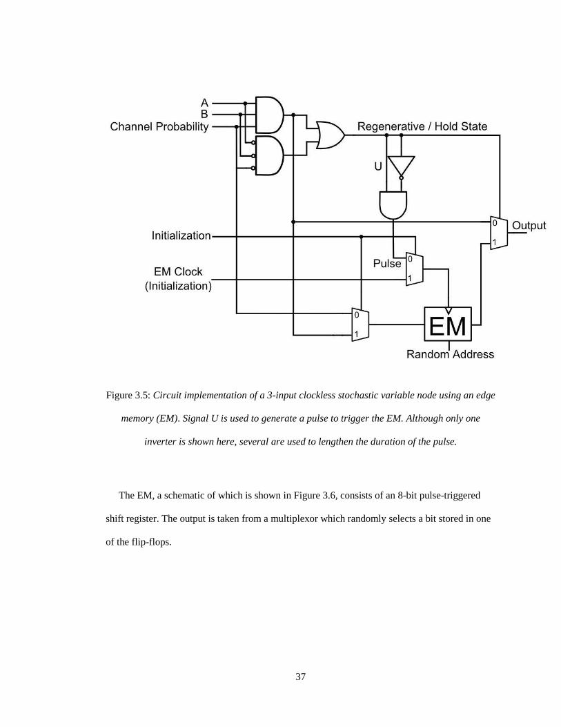
The EM, a schematic of which is shown in Figure 3.6, consists of an 8-bit pulse-triggered
shift register. The output is taken from a multiplexor which randomly selects a bit stored in one
of the flip-flops.
38
Figure 3.6: Schematic of the edge memory (EM) used in the clockless stochastic variable node.
3.7 Parity-Check Nodes
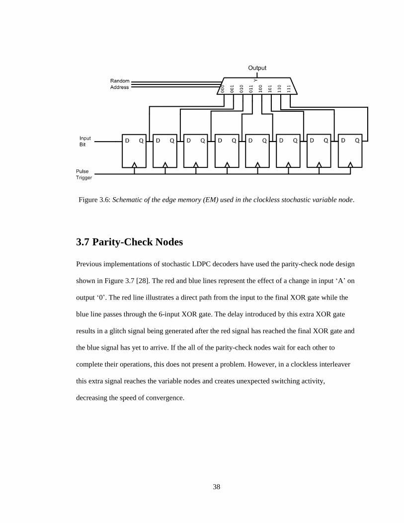
Previous implementations of stochastic LDPC decoders have used the parity-check node design
shown in Figure 3.7 [28]. The red and blue lines represent the effect of a change in input ‘A’ on
output ‘0’. The red line illustrates a direct path from the input to the final XOR gate while the
blue line passes through the 6-input XOR gate. The delay introduced by this extra XOR gate
results in a glitch signal being generated after the red signal has reached the final XOR gate and
the blue signal has yet to arrive. If the all of the parity-check nodes wait for each other to
complete their operations, this does not present a problem. However, in a clockless interleaver
this extra signal reaches the variable nodes and creates unexpected switching activity,
decreasing the speed of convergence.
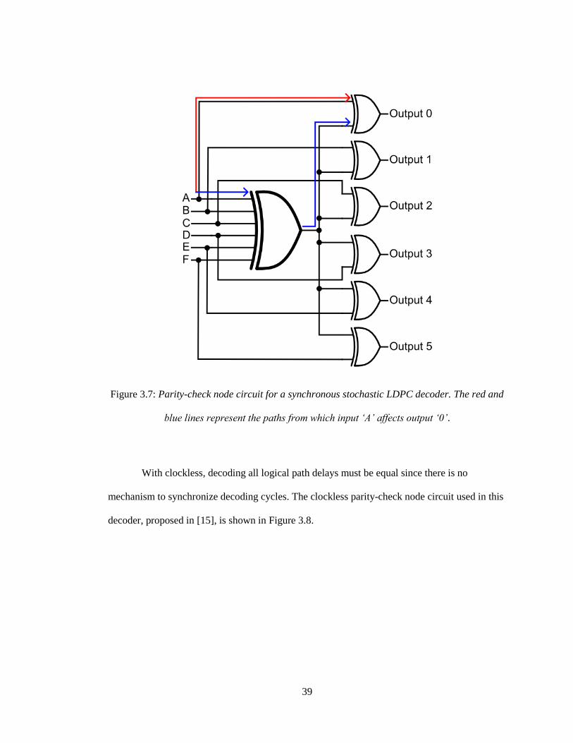
39
Figure 3.7: Parity-check node circuit for a synchronous stochastic LDPC decoder. The red and
blue lines represent the paths from which input ‘A’ affects output ‘0’.
With clockless, decoding all logical path delays must be equal since there is no
mechanism to synchronize decoding cycles. The clockless parity-check node circuit used in this
decoder, proposed in [15], is shown in Figure 3.8.
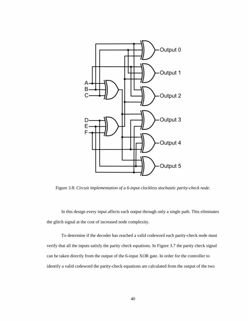
40
Figure 3.8: Circuit implementation of a 6-input clockless stochastic parity-check node.
In this design every input affects each output through only a single path. This eliminates
the glitch signal at the cost of increased node complexity.
To determine if the decoder has reached a valid codeword each parity-check node must
verify that all the inputs satisfy the parity check equations. In Figure 3.7 the parity check signal
can be taken directly from the output of the 6-input XOR gate. In order for the controller to
identify a valid codeword the parity-check equations are calculated from the output of the two
41
front-end XOR gates with an additional 2-input XOR gate required to calculated the parity-
check equations for all the inputs.
42
Chapter 4
Results and Discussion
This chapter reports the performance of the clockless stochastic LDPC decoder. Section 4.1
summarizes the FPGA logic utilization of the design. The frame error rate, throughput and
power measurements are presented in Section 4.2, 4.3, and 4.4, respectively.
4.1 Logic Utilization
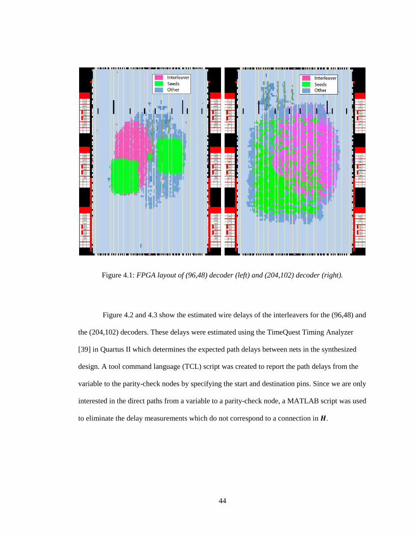
Table 4.1 shows the logic utilization of the (96,48) and (204,102) decoders while Figure 4.1
shows the chip layout of the FPGA with different modules highlighted. The stored seeds occupy
a significant portion of the decoder to ensure unique random switching activity high SNR tests
where many decoding frames are needed for a statistically significant number of errors. The
section labeled “other” includes the control module, the LFSRs, the LUTs associated with the
AWGN generator, and the comparators for stochastic bit generation. A larger (408,204) decoder
was also able to fit on the FPGA, however, due to the long compilation times this decoder was
not tested extensively.
43
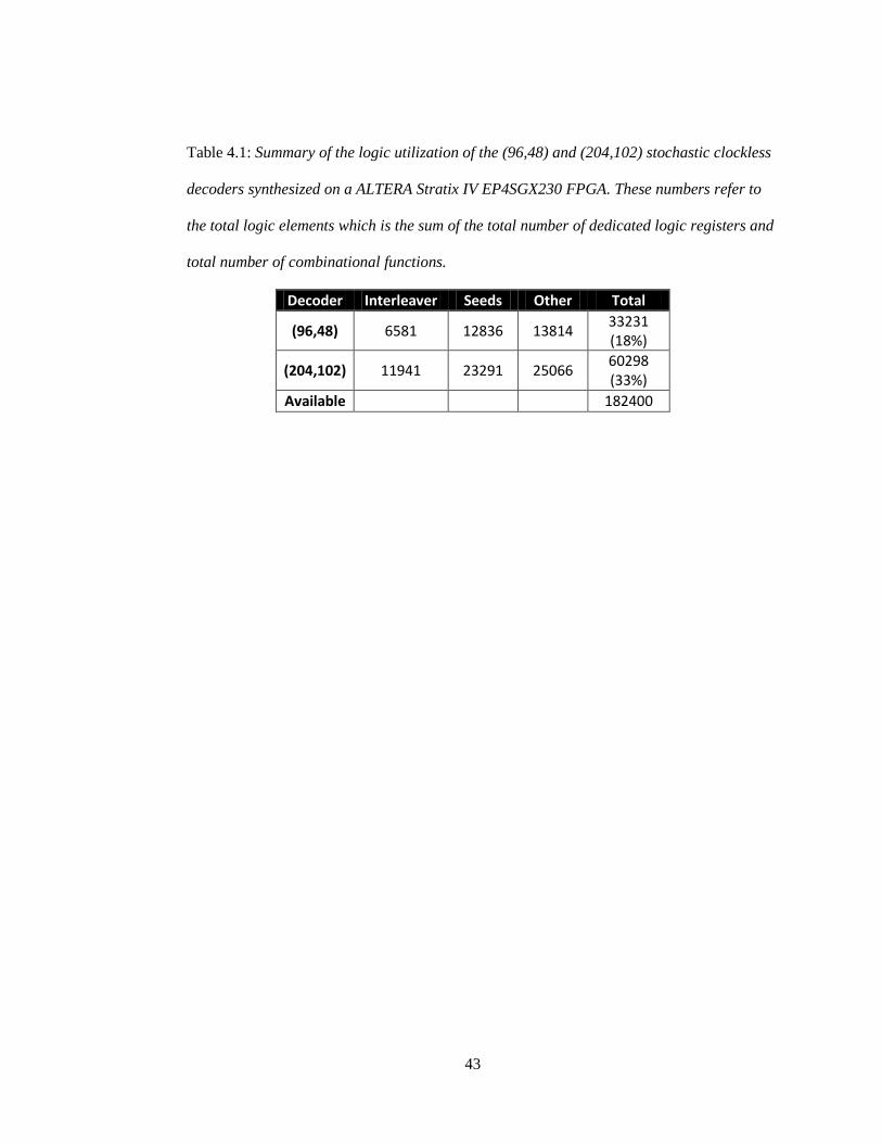
Table 4.1: Summary of the logic utilization of the (96,48) and (204,102) stochastic clockless
decoders synthesized on a ALTERA Stratix IV EP4SGX230 FPGA. These numbers refer to
the total logic elements which is the sum of the total number of dedicated logic registers and
total number of combinational functions.
Decoder Interleaver Seeds Other Total
(96,48) 6581 12836 13814 33231 (18%)
(204,102) 11941 23291 25066 60298 (33%)
Available
182400
44
Figure 4.1: FPGA layout of (96,48) decoder (left) and (204,102) decoder (right).
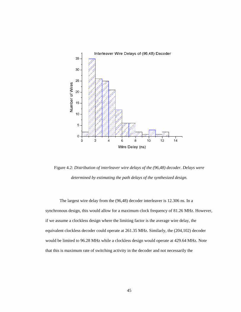
Figure 4.2 and 4.3 show the estimated wire delays of the interleavers for the (96,48) and
the (204,102) decoders. These delays were estimated using the TimeQuest Timing Analyzer
[39] in Quartus II which determines the expected path delays between nets in the synthesized
design. A tool command language (TCL) script was created to report the path delays from the
variable to the parity-check nodes by specifying the start and destination pins. Since we are only
interested in the direct paths from a variable to a parity-check node, a MATLAB script was used
to eliminate the delay measurements which do not correspond to a connection in 𝑯.
45
Figure 4.2: Distribution of interleaver wire delays of the (96,48) decoder. Delays were
determined by estimating the path delays of the synthesized design.
The largest wire delay from the (96,48) decoder interleaver is 12.306 ns. In a
synchronous design, this would allow for a maximum clock frequency of 81.26 MHz. However,
if we assume a clockless design where the limiting factor is the average wire delay, the
equivalent clockless decoder could operate at 261.35 MHz. Similarly, the (204,102) decoder
would be limited to 96.28 MHz while a clockless design would operate at 429.64 MHz. Note
that this is maximum rate of switching activity in the decoder and not necessarily the
46
throughput. That calculation would require an understanding of the decoding latency and the
relationship between the number of iterations and the bit error rate.
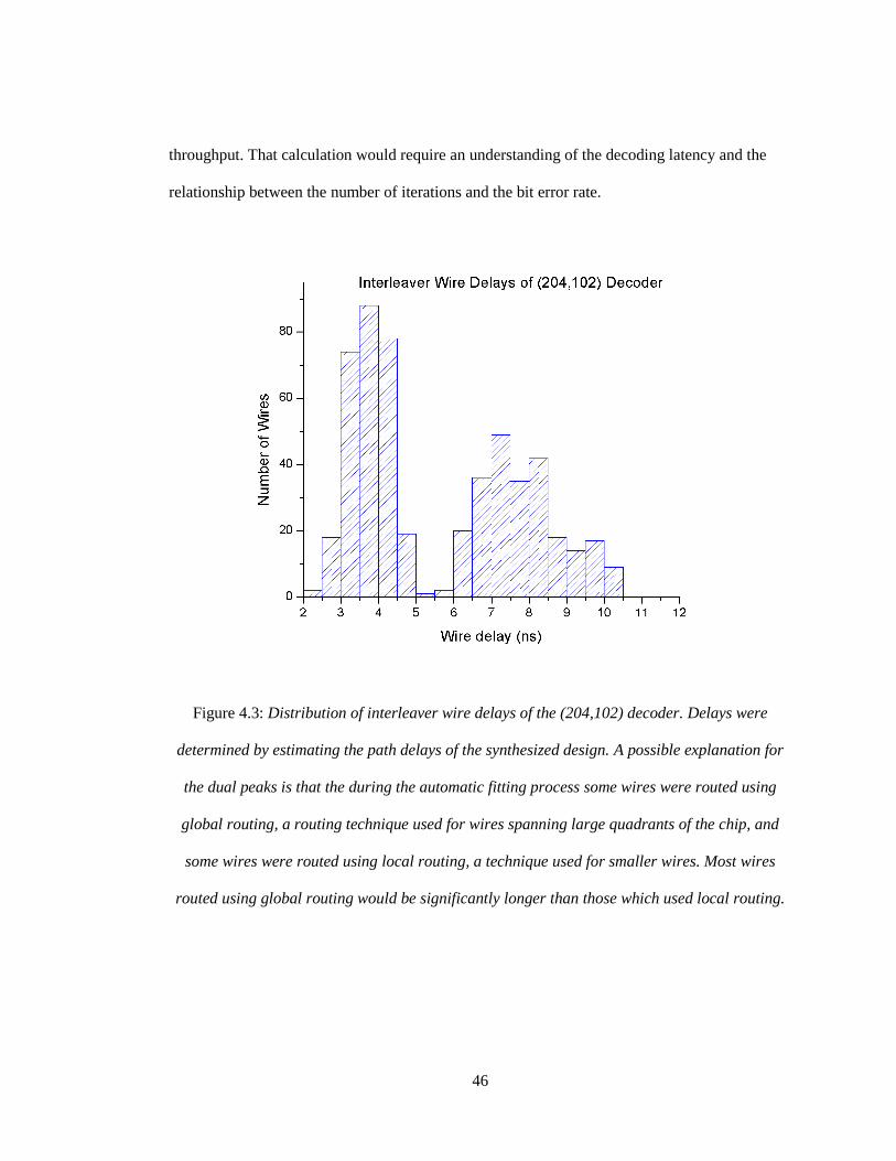
Figure 4.3: Distribution of interleaver wire delays of the (204,102) decoder. Delays were
determined by estimating the path delays of the synthesized design. A possible explanation for
the dual peaks is that the during the automatic fitting process some wires were routed using
global routing, a routing technique used for wires spanning large quadrants of the chip, and
some wires were routed using local routing, a technique used for smaller wires. Most wires
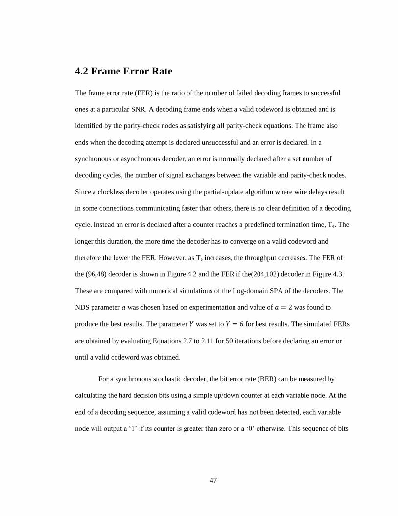
routed using global routing would be significantly longer than those which used local routing.
47
4.2 Frame Error Rate
The frame error rate (FER) is the ratio of the number of failed decoding frames to successful
ones at a particular SNR. A decoding frame ends when a valid codeword is obtained and is
identified by the parity-check nodes as satisfying all parity-check equations. The frame also
ends when the decoding attempt is declared unsuccessful and an error is declared. In a
synchronous or asynchronous decoder, an error is normally declared after a set number of
decoding cycles, the number of signal exchanges between the variable and parity-check nodes.
Since a clockless decoder operates using the partial-update algorithm where wire delays result
in some connections communicating faster than others, there is no clear definition of a decoding
cycle. Instead an error is declared after a counter reaches a predefined termination time, Te. The
longer this duration, the more time the decoder has to converge on a valid codeword and
therefore the lower the FER. However, as Te increases, the throughput decreases. The FER of
the (96,48) decoder is shown in Figure 4.2 and the FER if the(204,102) decoder in Figure 4.3.
These are compared with numerical simulations of the Log-domain SPA of the decoders. The
NDS parameter 𝑎 was chosen based on experimentation and value of 𝑎 = 2 was found to
produce the best results. The parameter 𝑌 was set to 𝑌 = 6 for best results. The simulated FERs
are obtained by evaluating Equations 2.7 to 2.11 for 50 iterations before declaring an error or
until a valid codeword was obtained.
For a synchronous stochastic decoder, the bit error rate (BER) can be measured by
calculating the hard decision bits using a simple up/down counter at each variable node. At the
end of a decoding sequence, assuming a valid codeword has not been detected, each variable
node will output a ‘1’ if its counter is greater than zero or a ‘0’ otherwise. This sequence of bits
48
can be compared with the original message to determine the number of bit errors. For a
clockless decoder, a time averaging circuit would be required at each variable node since there
are no clock cycles to trigger a counter. For the purposes of this thesis, it was decided that the
FER was sufficient for demonstrating the proof-of-concept decoder.
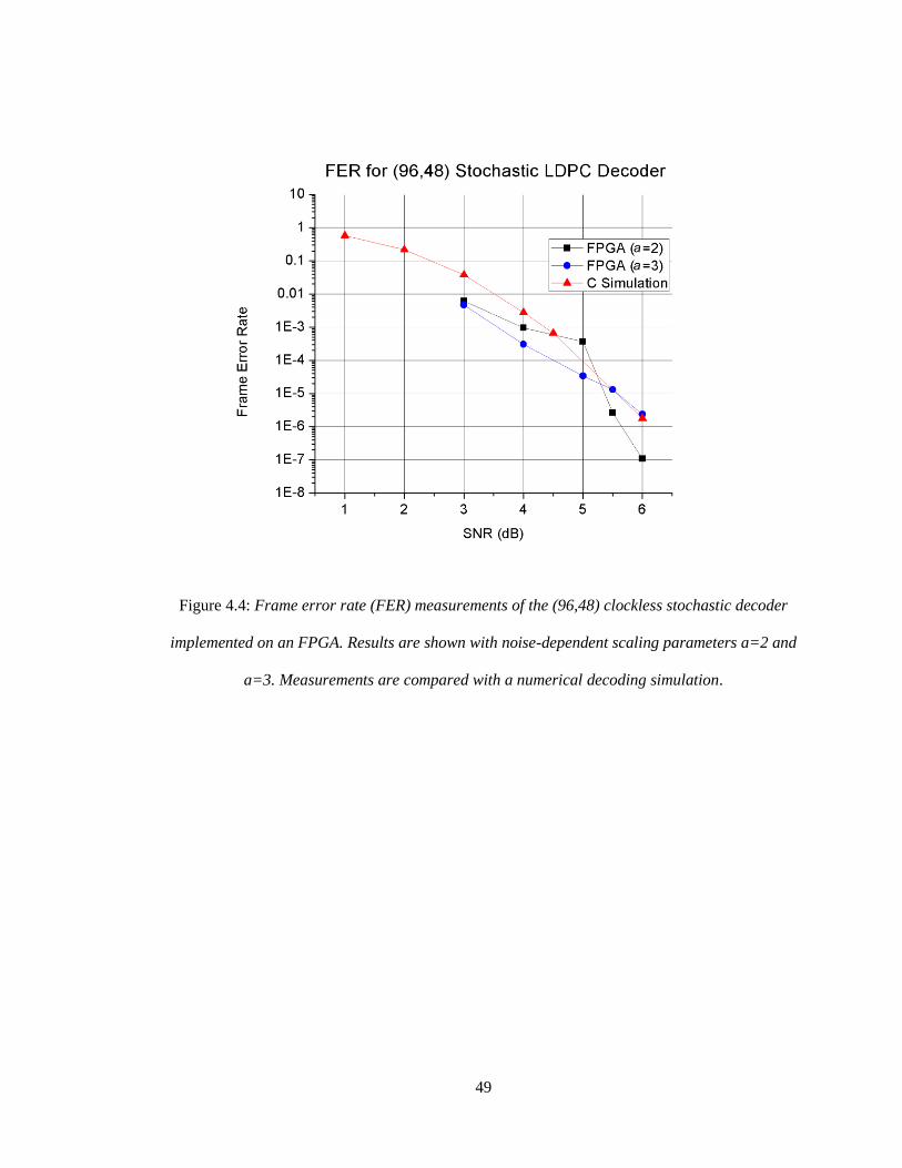
49
Figure 4.4: Frame error rate (FER) measurements of the (96,48) clockless stochastic decoder
implemented on an FPGA. Results are shown with noise-dependent scaling parameters a=2 and
a=3. Measurements are compared with a numerical decoding simulation.
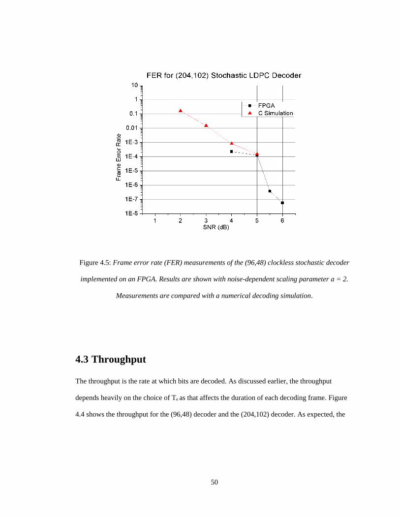
50
Figure 4.5: Frame error rate (FER) measurements of the (96,48) clockless stochastic decoder
implemented on an FPGA. Results are shown with noise-dependent scaling parameter a = 2.
Measurements are compared with a numerical decoding simulation.
4.3 Throughput
The throughput is the rate at which bits are decoded. As discussed earlier, the throughput
depends heavily on the choice of Te as that affects the duration of each decoding frame. Figure
4.4 shows the throughput for the (96,48) decoder and the (204,102) decoder. As expected, the
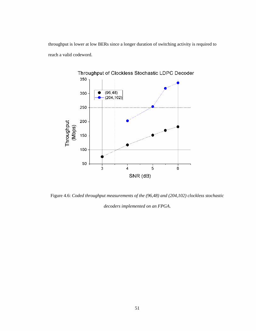
51
throughput is lower at low BERs since a longer duration of switching activity is required to
reach a valid codeword.
Figure 4.6: Coded throughput measurements of the (96,48) and (204,102) clockless stochastic
decoders implemented on an FPGA.
52
4.4 Power Measurements
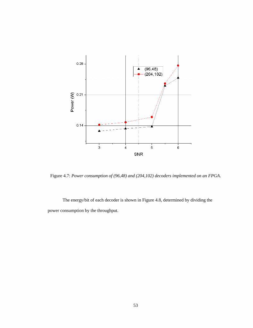
Since the throughput varies at different SNRs, so does the power consumption of the
decoder. The switching activity will also change, although this is minimized by the NDS. The
power consumptions of the (96,48) and (204,102) decoders are shown in Figure 4.5. The FPGA
power measurements were made using the technique developed by former MASc student Joyce
Li in [34]. Although Quartus II contains a module for estimating the power consumption based
on timing simulations, this technique has a large error [35]. The method used for power
measurements in this thesis measures the power delivered to the FPGA directly using a
voltmeter and a pair of 0.01Ω resistors. This power measurement is then subtracted from a
similar measurement of the FPGA programmed with minimal logic. More details of the power
measurement technique can be found in [34].
53
Figure 4.7: Power consumption of (96,48) and (204,102) decoders implemented on an FPGA.
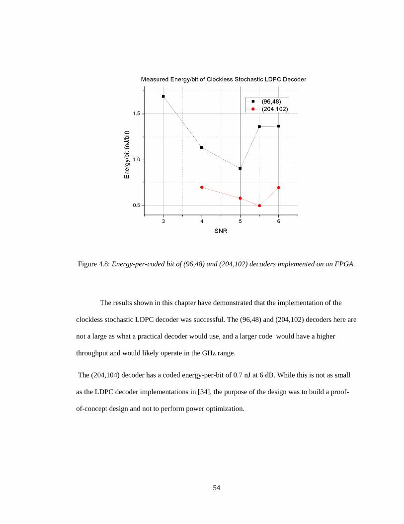
The energy/bit of each decoder is shown in Figure 4.8, determined by dividing the
power consumption by the throughput.
54
Figure 4.8: Energy-per-coded bit of (96,48) and (204,102) decoders implemented on an FPGA.
The results shown in this chapter have demonstrated that the implementation of the
clockless stochastic LDPC decoder was successful. The (96,48) and (204,102) decoders here are
not a large as what a practical decoder would use, and a larger code would have a higher
throughput and would likely operate in the GHz range.
The (204,104) decoder has a coded energy-per-bit of 0.7 nJ at 6 dB. While this is not as small
as the LDPC decoder implementations in [34], the purpose of the design was to build a proof-
of-concept design and not to perform power optimization.
55
Chapter 5
Conclusion
The advantages of stochastic LDPC decoders include lower wiring complexity and lower power
consumption. However, due to the serial nature of stochastic computing the throughput is
limited by the clock speed. A clockless implementation of this type of decoder eliminates this
limitation by allowing node computations to be completed purely through combinational logic.
In this thesis research, an implementation of a clockless stochastic LDPC decoder was
implemented on silicon. To our knowledge, this is the first implementation of its kind on an
FPGA.
The results reported in Chapter 4 show that the clockless stochastic LDPC was
successfully implemented on the FPGA. The clockless interleaver design eliminates the large
high-speed clock network present in synchronous decoders reducing the limitations that the wire
delays place on the throughput.
The HDL files for the decoder were generated using a C script and the FPGA was
programmed using Quartus II. The variable and check-nodes were designed to operate in
continuous time without the synchronization of node calculations. To reduce the noise floor and
increase the speed of convergence, EMs and NDS were employed to increase the switching
56
activity and therefore the speed of convergence. The large amount of random numbers required
for the AWGN generator and stochastic bit generation were produced using LFSRs with a seed
rotating technique that ensured that the decoder could evaluate many frames before repeating
random numbers.
The scaling parameters here were chosen based on optimal performance through
experimentation. However, a more detailed analysis of the error floor of this decoder is
necessary for a quantitative determination of the optimal parameter choices. This type of
analysis could also be used to predict the optimal clock speed for the generation of noise
channel stochastic bits and for EM addresses.
LDPC decoders suffer from error floors at high SNR. It is possible that continuous time
implementations will help to alleviate this issue in the future.
57
References
1 R. G. Gallager. Low Density Parity Check Codes. Cambridge, MA: MIT Press, 1963.
2 R. G. Gallager, “Low density parity check codes,” IRE Transactions Information
Theory, Jan. 1962, 8, (1), pp. 21-28.
3 C. Berrou, A. Glavieux, P. Thitimajshima, “Near Shannon limit error-correcting coding
and decoding: Turbo-codes,” IEEE International Conference on Communications,
Geneva. Technical Program, Conference Record, May 1993, 2, pp. 1064-1070.
4 D. MacKay and R. Neal, “Near Shannon limit performance of low density parity check
codes,” Electronics Letters, Aug. 1996, 32, (18), pp. 1645.
5 D. MacKay, “Good error-correcting codes based on very sparse matrices,” IEEE
Transactions on Information Theory, Mar. 1999, 45, (2), pp. 399-431.
6 C. Schlegel and L. Perez, Trellis and Turbo Coding. Piscataway, NJ: IEEE Press, 2004.
7 N. Traore, S. Kant, T. L. Jensen, (2007). Message Passing Algorithm and Linear
Programming Decoding for LDPC and Linear Block Codes. Unpublished project,
Aalborg University, Aalborg, Denmark.
58
8 M. R. Islam, D. S. Shafiullah, M. M. A. Faisal, I. Rahman, “Optimized Min-Sum
Decoding Algorithm for Low Density Parity Check Codes,” International Journal of
Advanced Computer Science and Applications, 2011, 2, (12), pp. 168-174.
9 D. Haley, A. Grant, J. Buetefuer, “Iterative Encoding of Low-Density Parity-Check
Code,” IEEE Global Telecommunications Conference, Nov. 2002, 2, pp. 1289-1293.
10 R. M. Tanner, “A recursive approach to low complexity codes,” IEEE Transactions on
Information Theory, Sept. 1981, 27, (5), pp. 533-547.
11 N. Onizawa, T. Hanyu, and V. Gaudet, “Design of high-throughput fully-parallel LDPC
decoders based on wire partitioning,” IEEE Trans.Very Large Scale Integr. (VLSI)
Syst., 18, (3), pp. 482-489, Mar. 2010.
12 N. Onizawa, V. C. Gaudet, T. Hanyu, W. J. Gross, “Asynchronous Stochastic Decoding
of Low-Density Parity-Check Code,” IEEE 42nd International Symposium on Multiple-
Valued Logic, May 2012, pp. 92-97.
13 N. Onizawa, W. J. Gross, T. Hanyu, V. C. Gaudet, “Lowering Error Floors in
Stochastic Decoding of LDPC Codes Based on Wire-Delay Dependent Asynchronous
Updating,” IEEE 43rd International Symposium on Multiple-Valued Logic, May 2013,
pp. 254-259.
14 N. Onizawa, W. J. Gross, T. Hanyu, V. C. Gaudet, " Low-energy asynchronous
interleaver for clockless fully parallel LDPC decoding." IEEE Transactions on Circuits
and Systems I: Regular Papers, Aug. 2011, 58, (8), pp. 1933-1943.
15 N. Onizawa, W. J. Gross, T. Hanyu, V. C. Gaudet, "Clockless stochastic decoding of
low-density parity-check codes," IEEE Workshop on Signal Processing Systems, Oct.
2012, pp. 143-148.
59
16 F. R. Kschischang, B. J. Frey , H. A. Loeliger, " Factor Graphs and the Sum-Product
Algorithm," IEEE Transaction on Information Theory, 2001, 47, (2), pp.498-519.
17 V. K. Mansinghka, E. M. Jonas, and J. B. Tenenbaum, Computer Science and Artificial
Intelligence Laboratory Technical Report, Stochastic Digital Circuits for Probabilistic
Inference. Accessed February 13, 2014 [Online].
18 V. K. Mansinghka, E. M. Jonas, and J. B. Tenenbaum, Computer Science and Artificial
Intelligence Laboratory Technical Report, Stochastic Digital Circuits for Probabilistic
Inference. Accessed February 13, 2014 [Online].
Available: http://dspace.mit.edu/bitstream/handle/1721.1/43712/MIT-CSAIL-TR-2008-
069.pdf.
19 N. Onizawa, T. Hanyu, and V. Gaudet, “High-throughput bit-serial LDPC decoder LSI
based on multiple-valued asynchronous interleaving,” IEICE Trans. Electron., E92-C,
(6), pp. 867-874, Jun. 2009.
20 N. Onizawa, T. Ikeda, T. Hanyu, and V. C. Gaudet, “3.2-Gb/s 1024-brate-1/2 LDPC
decoder chip using a flooding-type update-schedule algorithm,” Proc. IEEE Midwest
Symp. Circuits and Systems, Aug. 2007, pp. 217-220.
21 N. Onizawa, T. Hanyu, and V. Gaudet, “Design of high-throughput fully-parallel LDPC
decoders based on wire partitioning,” IEEE Trans.Very Large Scale Integr. (VLSI)
Syst., 18, (3), pp. 482-489, Mar. 2010.
22 D. J. C. MacKay. Encyclopedia of Sparse Graph Codes,
http://www.inference.phy.cam.ac.uk/mackay/codes/data.html.
60
23 E. Boutillon , J. Danger , A. Ghazel, H. Laamari, “Efficent FPGA implementeation of
Gaussian noise generator for communication channel emulation,” 7th IEEE
International Conference on Electronics, Circuits & Systems, 2000, 1, pp. 366-369.
24 Y. Fan, Z. Zilic, “A novel scheme of implementing high speed AWGN communication
channel emulators in FPGAs,” Proceedings of the 2004 International Symposium on
proceeding of Circuits and Systems, 2004, 2.
25 P. Alfke, XILINX, Efficient Shift Registers, LFSR Counter and Long Pseudo-Random
Sequence Generators. Accessed March 27, 2014 [Online]. Available:
http://www.xilinx.com/support/documentation/application_notes/xapp052.pdf.
26 Maxim integrated, Pseudo-Random Number Generation touting for the MAX765x
Microprocessor. Accessed January 21, 2014 [Online]. Available:
http://www.maximintegrated.com/app-notes/index.mvp/id/1743.
27 S. S. Tehrani, S. Mannor, W. J. Gross, “Fully Parallel Stochastic LDPC Decoders,”
IEEE Transactions on Signal Processing, Oct. 2008, 56, 11, pp. 5692-5703.
28 K. Huang, V. Gaudet, M. Salehi, “A Markov chain model for Edge Memories in
stochastic decoding of LDPC codes,” 2011 45th Annual Conference on Information
Sciences and Systems (CISS), March 2011, pp. 1-4.
29 W.J. Gross, V.C. Gaudet, A. Milner, “Stochastic Implementation of LDPC Decoders,”
Conference Record of the Thirty-Ninth Asilomar Conference on Signals, Systems and
Computers, Oct. 2005, pp. 713-717.
30 C. Winstead, V.C. Gaudet, A. Rapley, C. Schlegel, “Stochastic iterative decoders,”
Proceedings. International Symposium on Information Theory, Sept. 2005, pp. 1116-
1120.
61
31 S. S. Tehrani, W. J. Gross, S. Mannor, “Stochastic decoding of LDPC codes,” IEEE
Communications Letters, Oct. 2006, 10, 10, pp. 716-718.
32 S. S. Tehrani, S. Mannor, W.J Gross, “An Area-Efficient FPGA-Based Architecture for
Fully-Parallel Stochastic LDPC Decoding,” IEEE Workshop on Signal Processing
Systems, Oct. 2007, pp. 255-260.
33 Tehrani S. S. (2011). Stochastic Decoding of Low-Density Parity-Check Coder.
Unpublished doctoral dissertation, University of Waterloo, Waterloo, Ontario, Canada.
34 S. Li (2012). Power Characterization of a Gbit/s FPGA Convolutional LDPC Decoder.
Unpublished Master of Applied Science dissertation, University of Waterloo, Waterloo,
Ontario, Canada.
35 Quartus II Handbook, version 13.1. Accessed March 27, 2014 [Online].
Available: http://www.altera.com/literature/hb/qts/quartusii_handbook.pdf.
36 ALTERA Stratix IV Device Handbook, Volume 1. Accessed Match 14, 2014 [Online].
Available: http://www.altera.com/literature/hb/stratix-iv/stx4_5v1.pdf.
37 S. J. Johnson, Introducing Low-Density Parity-Check Codes. Accessed October, 2013
[Online]. Available: http://sigpromu.org/sarah/SJohnsonLDPCintro.pdf.
38 W. E. Ryan, An Introduction to LDPC Codes. Accessed October, 2013 [Online].
Available: http://tuk88.free.fr/LDPC/ldpcchap.pdf.
39 ALTERA The Quartus II TimeQuest Timing Analyzer, Volume 3. Accessed May 20,
2014 [Online]. Available: http://www.altera.com/literature/hb/qts/qts_qii53018.pdf.
62
40 J. Von Neumann, “Probabilistic logics and the synthesis of reliable organisms from
unreliable components,” Automata studies 34, 1956, pp. 43-98.
41 V.C. Gaudet, A. Rapley, “Iterative decoding using stochastic computation,” Electronics
Letters, Feb. 2003, 39, (3), pp. 299-301.
42 M.P.C. Fossorier, M. Mihaljevic, H. Imai, “Reduced complexity iterative decoding of
Low-Density Parity Check codes based on belief propagation,” IEEE Transactions on
Communications, May 1999, 47, (5), pp. 673-680.
43 N. Onizawa, W. J. Gross, T. Hanyu, V. C. Gaudet, “Clockless Stochastic Decoding of
Low-Density Parity-Check Codes: Architecture and Simulation Model,” Journal of
Signal Processing Systems, Feb. 2013, ISBN: 1939-8018.