25
Hermes Microvision, Inc. Investor Presentation March 2015

Hermes Microvision, Inc.
Investor Presentation
March 2015
I. Introduction to HMI
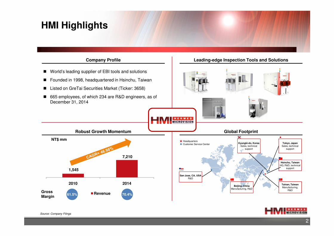
HMI Highlights
Company Profile Leading-edge Inspection Tools and Solutions
� World’s leading supplier of EBI tools and solutions
� Founded in 1998, headquartered in Hsinchu, Taiwan
� Listed on GreTai Securities Market (Ticker: 3658)
� 665 employees, of which 234 are R&D engineers, as of December 31, 2014
2
1,545
7,210
2010 2014
Revenue
Global FootprintRobust Growth Momentum
Gross Margin
70.4%61.5%
San Jose, CA, USAR&D
Tokyo, JapanSales, technical
support
Kyungki-do, KoreaSales, technical
support
Tainan, TaiwanManufacturing,
R&D
Beijing, ChinaManufacturing, R&D
Customer Service Center
Headquarters
Hsinchu, TaiwanHQ, R&D, technical
support
Source: Company Filings
NT$ mm
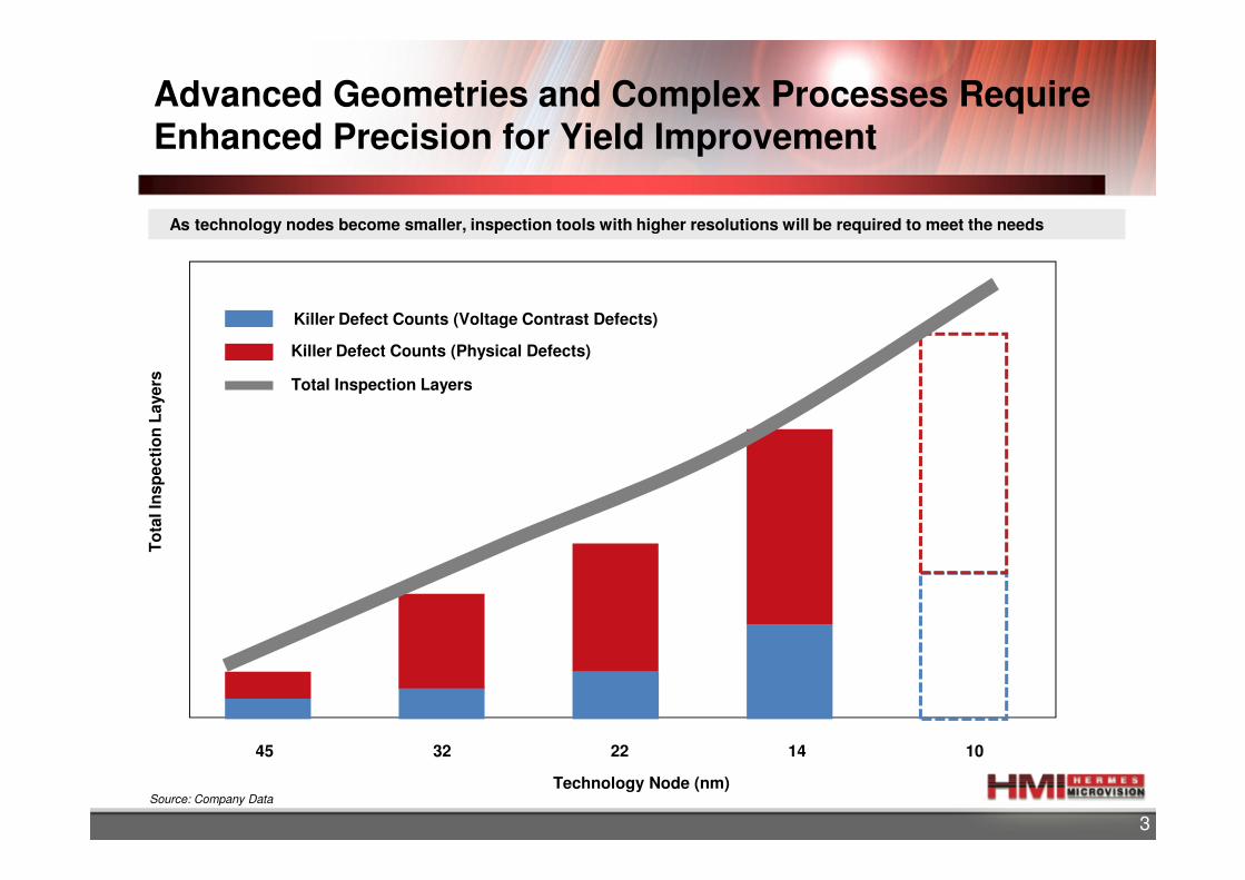
As technology nodes become smaller, inspection tools with higher resolutions will be required to meet the needs
Advanced Geometries and Complex Processes Require Enhanced Precision for Yield Improvement
Killer Defect Counts (Physical Defects)
Killer Defect Counts (Voltage Contrast Defects)
Total Inspection Layers
To
tal In
sp
ecti
on
Layers
3
Source: Company Data
45 32 22 14 10
Technology Node (nm)
To
tal In
sp
ecti
on
Layers
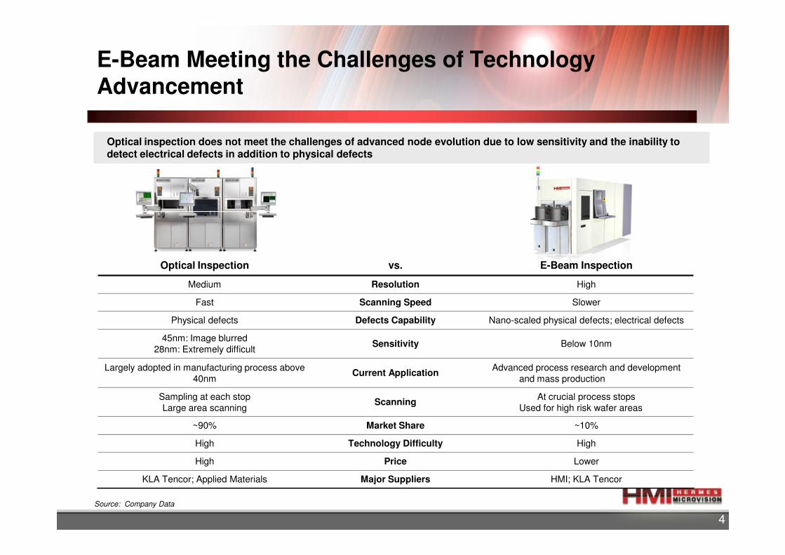
Optical inspection does not meet the challenges of advanced node evolution due to low sensitivity and the inability to detect electrical defects in addition to physical defects
E-Beam Meeting the Challenges of Technology Advancement
Optical Inspection vs. E-Beam Inspection
4
Medium Resolution High
Fast Scanning Speed Slower
Physical defects Defects Capability Nano-scaled physical defects; electrical defects
45nm: Image blurred
28nm: Extremely difficultSensitivity Below 10nm
Largely adopted in manufacturing process above
40nm Current Application
Advanced process research and development
and mass production
Sampling at each stop
Large area scanning Scanning
At crucial process stops
Used for high risk wafer areas
~90% Market Share ~10%
High Technology Difficulty High
High Price Lower
KLA Tencor; Applied Materials Major Suppliers HMI; KLA Tencor
Source: Company Data

Overview of HMI’s Product PortfolioDiversified Product Offerings and Capabilities
Process OptimizationEarly discovery of defect to increase yield and reduce cost
Wafer Inspection In-line Monitoring Defect Analysis
ePTM Series eScan® Series SupernovaTM
5
Product ePTM4 eScan®500 eScan®400 SkyScanTM5000 NanoScanTM2000 SupernovaTM
DescriptionHotspot inspection and CDU process monitoring system
Highest sensitivity for large-area defect
inspection
High throughput defect inspection
Millions+ hotspot in-line monitoring
Application-specificin-line monitoring
Advanced D2DB inspection system and defect Analytics
Key Advantages
� Highest detection sensitivity to physical defects
� Innovative platform to enable highest scan throughput
� Built-in GDS engine to expand the use space of powerful CDU methodology to inline monitor process drift and effective hot-spot monitoring
� Suitable for 10nm and 7nm nodes
� Longest lifetime for advanced fabs� Highest sensitivity to defect of interest
signature detection in large area or full die
� Effective for litho induced DOIs for OPC improvement
� Highest image fidelity and linearity in large scan area for advanced D2DB inspection
� Most advanced defect binning algorithm� Suitable for 14nm and 10nm nodes
� Largest area coverage with highest defect sensitivity for inline process control
� Proprietary technology for precision positioning of stage and e-beam on the fly
� Vector scan technology to focus on potential hot spots for high resolution with low queue time for inline monitoring
� Suitable for 14nm and 10nm ramp and HVM
� Cost-efficient high throughput in-line CDU monitoring
� Advanced defect detection algorithms with HMI’s unique CDU capability enables quick feedback for inline monitoring
� Advanced defect review and classification algorithm for ease of control process excursion
� Advanced GDS D2DB inspection for most demanding defect capturing, analysis, and classification analytics
� In-line D2DB analysis with instantaneous defect report for fast R&D cycles;
� Unique D2DB algorithm with highest defect capture and lowest nuisance
Scan Mode Hotspot Inspection Multi-Function Continuous Scan Vector Scan Hotspot Monitoring
Mainstream application
Logic / Memory Logic / Memory Memory Logic Logic / Memory
Design / Manufacturing
In-house In-house In-house In-houseIn-house
Highest Resolution
2nm 3nm 10nm 3nm 2nm
Source: Company Filings,
Company Website
II. Key Investment Highlights

Key Investment Highlights
1 Clear Beneficiary of Fast Growing Semiconductor Process Control Segment
2 Leading Expertise in E-Beam Inspection Technology
3 Strong Partnerships with Industry Leaders Based on Technology and Services
7
3 Strong Partnerships with Industry Leaders Based on Technology and Services
4 Integrated Business Model Delivering Superior Operating Efficiency

Industry Transitioning to Smaller Technology Nodes
1 Clear Beneficiary of Fast Growing Semiconductor Process Control Segment
1995 2000 2002 2006 2008 2010 2012 2014 2016 2018 2020
350nm 130nm 90nm 65nm 45nm 32nm 28nm 14nm 10nm 7nm 5nm 2nm
…
8
14.6% 7.3% 13.9%
26.3%
14.5%3.4%
42.1%
41.4%35.7%
15.6%
22.3%
9.1%
1.4%
14.5%
37.9%
2012 2014 2018E
65 nm and above 45 nm 32 nm 22 nm 14 nm and below
2013 2018E
Source: Company Filings, Gartner Research
Increasing Importance of Advanced Technology Nodes
To
tal S
em
ico
nd
ucto
r W
afe
r F
ab
Eq
uip
men
t
(U
S$b
n)
Investment in Process Control Tools on the Rise
Pro
cess C
on
tro
l C
ap
ex
(in
cl.
OE
M)
(
US
$b
n)
$5.6bn
350nm 130nm 90nm 65nm 45nm 32nm 28nm 14nm 10nm 7nm 5nm 2nm
$30.0bn $31.6bn $39.1bn
$3.9bn

20132014
E-Beam12%
E-Beam14%
1 Clear Beneficiary of Fast Growing Semiconductor Process Control Segment
The distinct advantages of EBI over optical at advanced technology nodes encourages increasing adoption of EBI in wafer inspection. HMI continues to focus on new growth initiatives that include high productivity, low CoO and massive parallel scanning technologies/tools for HVM inline applications
2015EE-Beam
9
Source: Company Filings, Gartner Research
Optical88%
Optical
Inspection Market: US$1.6bn Inspection Market: US$1.7bn
OpticalOptical86% Optical

65
40
40
50
60
70
(nm)
HMI has achieved approximately a 30% improvement in resolution with every generation of tech node evolution
2 Leading Expertise in E-Beam Inspection Technology
10
28
20
14105/3
0
10
20
30
2006 2008 2010 2012 2013 2014
R&D Node HMI E-Beam Inspection Resolution
eScan300
eScan310
eScan315xpeScan320 / eP3 eScan500 eP4
HMI is committed to leading technology innovation through R&D
Source: Company filings

Strong Partnerships with Industry Leaders Based on Technology and Services
� HMI teams up with customers in R&D and shares the benefits of innovation
� HMI customizes to meet different needs
� HMI provides instant customer service globally
3
Top IDMs1
HMI’s Winning Business ModelPartnerships for Long-term Success
11
� HMI provides instant customer service globally
— Our customer service centers are located where our customers are located
Source: Company Filings, Gartner Research
Top Foundries
1 IDM (Integrated Device Manufacturers) includes both logic and memory IC companies.

Key Technologies Multi-Disciplinary R&D Team
� Designs all and manufacturers 80% of the key components, modules
and systems in-house, which ensures uniqueness, quality,
performance and lifetime of products while providing cost advantages
� Extensive technological expertise in:
— E-Beam system: e-optics, deflection, imaging
— Algorithm: image comparison and defect detection
— Mechanical systems: vacuum and precision movement
+Taiwan 82 R&D
Engineers
Taiwan 82 R&D
Engineers +US
117 R&D Engineers
US117 R&D
Engineers
China35 R&D
Engineers
China35 R&D
Engineers
Optical PhysicsOptical Physics
Image Processing
Image Processing
Mechanical Structure
Mechanical Structure
AlgorithmAlgorithm
Electron Electron SoftwareSoftware
Electronics Electronics Digital & Analog
Digital & Analog
4 Integrated Business Model Delivering Superior Operating Efficiency
12
— Mechanical systems: vacuum and precision movement
— GDS analysis: defect tracking and analysis database
Electron Optics
Electron Optics
SoftwareSoftwareElectronics & Control
Electronics & Control
Analog DesignAnalog Design
Strong Operating Leverage
Source: Company Filings
Operating Expense as % of Revenues2010 – 2014 Revenue CAGR: 46.98%
2010 – 2014 Opex CAGR: 21.95%53.8%
41.8%
30.5%25.2% 25.5%
2010 2011 2012 2013 2014
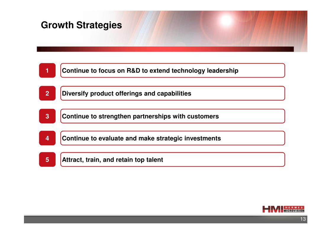
Growth Strategies
1 Continue to focus on R&D to extend technology leadership
2 Diversify product offerings and capabilities
3 Continue to strengthen partnerships with customers
13
3 Continue to strengthen partnerships with customers
4 Continue to evaluate and make strategic investments
5 Attract, train, and retain top talent

III. Financial Highlights
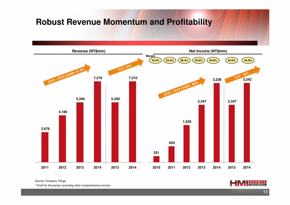
Robust Revenue Momentum and Profitability
Revenue (NT$mm) Net Income (NT$mm)Margin
16.3% 24.4% 36.4% 44.0%44.0%
5,340
7,210
5,340
7,210
2,347
3,238
2,347
3,242
44.9% 44.9%
15
Source: Company Filings
* Profit for the period, excluding other comprehensive income.
2,678
4,180
2011 2012 2013 2014 2013 2014
251
654
1,520
2,347 2,347
2010 2011 2012 2013 2014 2013 2014
21.8%
14.3%
53.8%
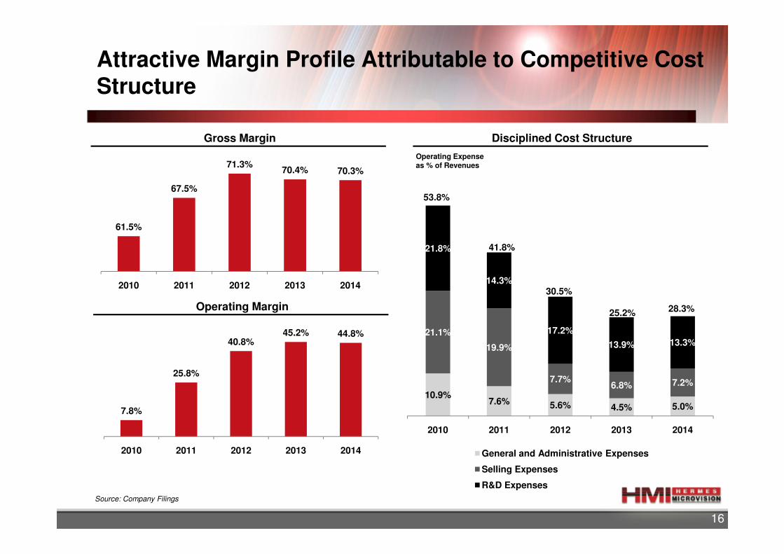
Attractive Margin Profile Attributable to Competitive Cost Structure
Disciplined Cost StructureGross Margin
Operating Expense as % of Revenues
41.8%
61.5%
67.5%
71.3%70.4% 70.3%
16
10.9%7.6% 5.6% 4.5% 5.0%
21.1%
19.9%
7.7%6.8% 7.2%
14.3%
17.2%
13.9% 13.3%
2010 2011 2012 2013 2014
General and Administrative Expenses
Selling Expenses
R&D Expenses
Operating Margin
Source: Company Filings
30.5%
25.2% 28.3%
2010 2011 2012 2013 2014
7.8%
25.8%
40.8%45.2% 44.8%
2010 2011 2012 2013 2014
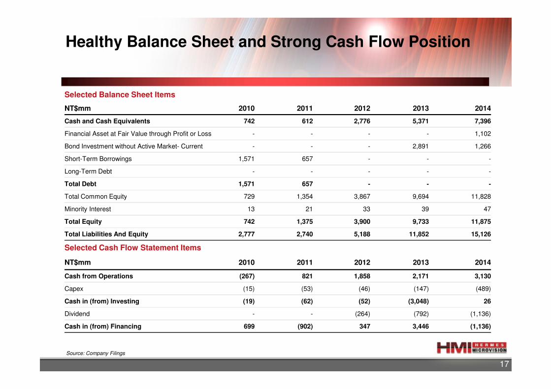
Healthy Balance Sheet and Strong Cash Flow Position
Selected Balance Sheet Items
NT$mm 2010 2011 2012 2013 2014
Cash and Cash Equivalents 742 612 2,776 5,371 7,396
Financial Asset at Fair Value through Profit or Loss - - - - 1,102
Bond Investment without Active Market- Current - - - 2,891 1,266
Short-Term Borrowings 1,571 657 - - -
Long-Term Debt - - - - -
Total Debt 1,571 657 - - -
Total Common Equity 729 1,354 3,867 9,694 11,828
17
Total Common Equity 729 1,354 3,867 9,694 11,828
Minority Interest 13 21 33 39 47
Total Equity 742 1,375 3,900 9,733 11,875
Total Liabilities And Equity 2,777 2,740 5,188 11,852 15,126
Selected Cash Flow Statement Items
NT$mm 2010 2011 2012 2013 2014
Cash from Operations (267) 821 1,858 2,171 3,130
Capex (15) (53) (46) (147) (489)
Cash in (from) Investing (19) (62) (52) (3,048) 26
Dividend - - (264) (792) (1,136)
Cash in (from) Financing 699 (902) 347 3,446 (1,136)
Source: Company Filings

APPENDIX
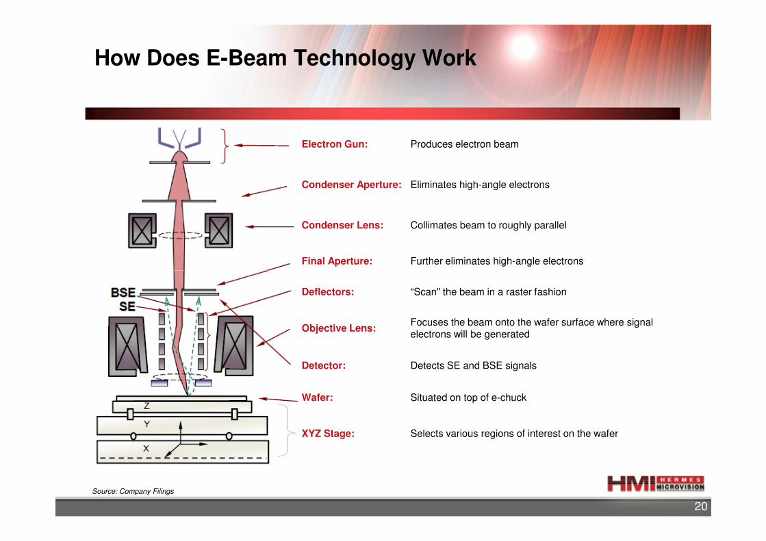
How Does E-Beam Technology Work
Electron Gun: Produces electron beam
Condenser Aperture: Eliminates high-angle electrons
Condenser Lens: Collimates beam to roughly parallel
Final Aperture: Further eliminates high-angle electrons
20
Deflectors: “Scan" the beam in a raster fashion
Objective Lens:Focuses the beam onto the wafer surface where signal electrons will be generated
Detector: Detects SE and BSE signals
Wafer: Situated on top of e-chuck
XYZ Stage: Selects various regions of interest on the wafer
Source: Company Filings

History and Key Milestones
2013 YTD
� Hermes Microvision, Inc., USA incorporated in Silicon Valley to focus on R&D for EBI equipment
� HMI founded in
� Beijing subsidiary established
� Japan branch established
� Japan and Korea subsidiaries established
� Registered as a public company
� Set up branch in Hsinchu Science Park
� Listed on GTSM in May 2012 with ticker “3658”
� Successfully developed eScan®500
� Issued GDR
� Successfully developed ePTM4
21
Source: Company Filings
19982003
20042005
2006
2007
2008
2009
2010
2012
� The first EBI tool (eScan®300) was successfully developed
� HMI founded in Hsinchu, Taiwan
� Entered Japan and Korea markets
� Successfully developed eScan®320, eXplore® and SuperNovaTM
� Received “2010 Best Tool Delivery and Technical Support” from TSMC
� Developed ePTM2, eScan Lite and eScan®315
� Developed eScan®310 and eScan®380
� Received “2006 Supplier Excellence Awards in E-beam Inspection” from TSMC
� Successfully developed eScan®400
� Successfully developed ePTM3
� Received “2011 Excellent Tool Delivery and Installation Support” from TSMC
eScan®500

Summary Income Statement
NT$mm, unless otherwise stated 2010 2011 2012 2013 2014
Total Revenue 1,545 2,678 4,180 5,340 7,210
YoY Growth % 32.3% 73.3% 56.1% 27.8% 35.0%
Gross Profit 951 1,808 2,981 3,758 5,065
Margin % 61.5% 67.5% 71.3% 70.4% 70.3%
Operating Expenses (831) (1,118) (1,274) (1,347) (1,837)
22
As % of Total Revenue (53.8)% (41.8)% (30.5)% (25.2)% (25.5)%
Operating Income 120 690 1,707 2,412 3,228
Margin % 7.8% 25.8% 40.8% 45.2% 44.8%
Net Income 251 654 1,520¹ 2,347¹ 3,242¹
Margin % 16.3% 24.4% 36.4% 44.0% 45.0%
Diluted EPS (NT$) 6 11 23 35 46
YoY Growth % NM 89.5% 116.1% 50.3% 30.0%
Source: Company Filings
¹ Profit for the period, excluding other comprehensive income.

Summary Balance Sheet
NT$mm 2010 2011 2012 2013 2014
Cash and Cash Equivalents 743 612 2,776 5,371 7,396
Financial Asset at Fair Value through Profit or Loss - - - - 1,102
Bond Investments without Active Markets- Current - - - 2,891 1,266
Accounts Receivable – Third Parties 722 653 848 1,557 2,662
Inventories, Net 1,074 1,190 1,279 1,516 1,745
Total Current Assets 2,587 2,523 4,972 11,444 14,298
23
2,587 2,523 4,972 11,444 14,298
Property, Plant and Equipment 132 168 170 335 750
Total Assets 2,777 2,740 5,188 11,852 15,126
Short-term Loans 1,571 657 - - -
Provisions for Liabilities – Current 130 219 577 972 1,471
Total Current Liabilities 2,008 1,300 1,199 2,035 3,162
Other Liabilities 27 65 89 84 89
Total Liabilities 2,035 1,365 1,288 2,119 3,251
Total Stockholders’ Equity 742 1,375 3,900 9,733 11,875
Total Liabilities and Stockholders’ Equity 2,777 2,740 5,188 11,852 15.126
Source: Company Filings

Summary Cashflow Statement
NT$mm 2010 2011 2012 2013 2014
Depreciation & Amortization 46 52 63 60 62
Cash from Operations (267) 821 1,858 2,171 3,130
Capex (15) (53) (46) (147) (489)
Cash from Investing (19) (62) (52) (3,048) 26
Dividend - - (264) (792) (1,136)
Cash from Financing 699 (902) 347 3,446 (1,136)
24
Source: Company Filings


