Abstract—Hash functions are used in the majority of securityprotocol to guarantee the integrity and the authenticity. Amongthe most important hash functions is the SHA-2 family, whichoffers higher security and solved the insecurity problems ofother popular algorithms as MD5, SHA-1 and SHA-0. However,theses security algorithms are characterized by a certain amountof complex computations and consume a lot of energy. Inorder to reduce the power consumption as required in themajority of embedded applications, a solution consists to exploita critical part on accelerator (hardware). In this paper, wepropose a hardware/software exploration for the implementationof SHA256 algorithm. For hardware design, two principal designmethods are proceeded: Low level synthesis (LLS) and high levelsynthesis (HLS). The exploration allows the evaluation of perfor-mances in term of area, throughput and power consumption.The synthesis results under Zynq 7000 based-FPGA reflect asignificant improvement of about 80% and 15% respectively inFPGA resources and throughput for the LLS hardware designcompared to HLS solution. For better efficiency, hardware IPs arededuced and implemented within HW/SW system on chip. Theexperiments are performed using Xilinx ZC 702-based platform.The HW/SW LLS design records a gain of 10% to 25% in termof execution time and 73% in term of power consumption.
Index Terms—SHA256, Zynq 7000 based-FPGA, LLS, HLS.
I. INTRODUCTION
Nowadays, the Field-Programmable Gate-Array (FPGA)is becoming a good alternative to the application-specificintegrated circuit (ASICs) especially when dealing with suchcomplex implementation like image or signal processing ap-plications [1]. Indeed, thinks to the progress brought onprogrammable circuits, it becomes possible to design a Sys-tem on Chip (SoC) component based on single or multipleprocessors and a programmable logic. This kind of systemcould be exploited in a wide range of applications for itsflexibility, short time to market, low power and high capacity
Manuscript received January 7, 2021; revised April 1, 2021. Date ofpublication April 29, 2021. Date of current version April 29, 2021. Theassociate editor prof. Toni Perkovic has been coordinating the review of thismanuscript and approved it for publication.
M. Kammoun is with the Digital Research Center of Sfax, Sfax,Tunisia. M. Elleuchi and M. Abid are with the CES Research Laboratory,National Engineering School of Sfax, Digital Research Center of Sfax,Sfax, Tunisia. A. M. Obeid is with the National Center for Electron-ics, Communications and Photonics at KACST (e-mails: [email protected], [email protected], mohamed.abid [email protected],[email protected]).
Digital Object Identifier (DOI): 10.24138/jcomss-2021-0006
of integration. In addition, the reconfigurability of FPGAcircuits boosts the designers to implement their own programsusing a Hardware Description Language (HDL) and also tomake several optimizations on the hardware architecture.
For decades, the Low-Level Synthesis (LLS) has beenadopted as a design method for FPGA implementations asit is more reliable and requires an explicit coding of thecontrol path. This option leads to better improve designcapabilities by optimizing whatever parameters. Nevertheless,the designing of the final netlist takes much time an effort,practically for the case of complex algorithms. At this level,the hardware developers are front of a new challenge wheremany constraints should be taken into account to fulfill themarket requirement. Consequently, it is time to think aboutnew design methods which can help to economize timingconstraint and facilitate the implementation task on FPGAs.The solution is to raise the abstraction level from LLS to HighLevel Synthesis (HLS) using a specific high level descriptionlanguage (Matlab, C/C++, etc...). For many reasons, the HLSbecomes more and more useful than LLS [2] [3]. One of thekey benefit of working with HLS is the ability to simulatemultiple algorithms in the shortest times [4]. Moreover,modern HLS tools such as (Vivado HLS [5], Catapult-C[6], etc..) are able to provide an estimative report of areacost, frequency and latency time more quickly. Also, severaloptimizations can be exploited at the level of C function tobetter improve design performances in term of throughput andhardware cost. For instance, the usage of pipeline an unrollpragmas can help to reach higher throughputs at the cost ofincreasing logical gates. However, there are some restrictionsthat should be held on before working with HLS tools. First,it is not a simple conversion from high level language toRTL level. In fact, the code must be re-written with a specificway to be correctly implemented on FPGA platform. Second,some particular C instructions based on pointer and recursionare not synthesizable and can cause memory overhead inthe context of FPGA. All these reasons prevent designers togo over optimizing more their architectures. Consequently,the main focus of this work will be devoted to study theinfluence of LLS and HLS design methods when facing asuch computational application like cryptographic algorithm.
Most of application domains use secure techniques and al-gorithms to protect them from attacks while respecting the se-
JOURNAL OF COMMUNICATIONS SOFTWARE AND SYSTEMS, VOL. 17, NO. 2, JUNE 2021 87
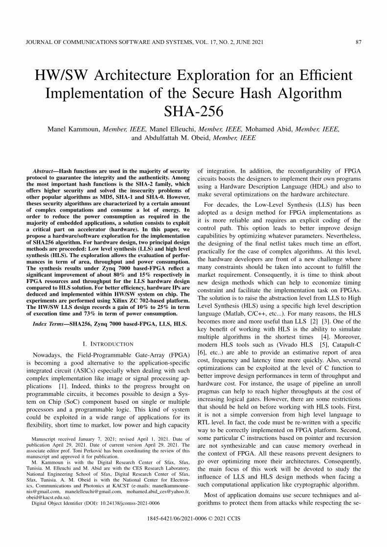
curity requirements. Several security protocol and frameworksare based on symmetric cryptographic techniques, Asymmetriccryptographic techniques, hybrid cryptography techniques andhash functions [7]. Hash functions are the most importantkey to keep data safe and secure. They are used as buildingblocks in various cryptographic and security services suchas electronic commerce, digital signature and informationauthentication. SHA-2 is a family of hash functions that weredesigned by the US National Security Agency (NSA), basedon SHA-1 and SHA-0. Like most of the hash functions, theSHA-2 takes as input a message of arbitrary size and producesa fixed size output.Fig. 1 represents a general model of thistype of functions [8].
The size of hash is indicated by the suffix: 224 bits forSHA-224, 256 bits for SHA-256 and 512 bits for SHA-512.Forinstance, SHA-256 is a type of secure hash operation under theSHA-2 [9] banner with digest length of 256 bits. This familyof hashing algorithms uses large digest messages making themmore resistant to possible attacks and allowing them to be usedwith big amount of data blocks, up to 2128bits in the case ofSHA-512.
The SHA-256 presents a model of hash algorithm thatposses many computational rounds. In this context, there is aproliferation of various works which were trying to optimizethe complexity of SHA-256 function using the hardware accel-erators as provided in [10] and [11]. However, these solutionssuffer from lack of flexibility and performance degradation. Toovercome these deficiencies, two design methods are adoptedin this work based on LLS and HLS synthesis. With system-on-chip (SoC) designs growing in complexity, system-levelapproaches that leverage on HLS and LLS techniques arebecoming the workhorse of current SoC design flows. Thesesolutions provide reasonable agreements in term of FPGAresources, throughput and power consumption. To highlightour contribution, the proposed LLS and HLS accelerators areintegrated in HW/SW context in order to estimate perfor-mances in term of execution time and power consumption.
The remainder of this paper is organized as follows. SectionII introduces some related works which had implementedSHA-256 algorithm under FPGA platform. Section III presentsour proposed architectures implemented on the Xilinx ZC702 evaluation board [12]. The experimental findings of theHW/SW implementations in term of throughput and powerconsumption are discussed in section IV. Finally, the conclu-sion and the futures works are provided in Section V.
II. RELATED WORKS
Several works had experimented the implementation ofcryptographic hash functions on FPGA-based platform. Forinstance, the example given in [13] proposed an improvedschemas of the SHA-256 algorithm implemented on Virtex-2 XC2VP-7. These designs were based on the rearrangementtechnique to compute the inner loop of the SHA-256 hashfunction such as computing values in advance and changingthe control path without increasing the clock cycles. In bestcase, the maximum throughput achieved in this work wasabout 909 Mbps with an efficiency of 0.713 Mbps/ slice.
In [14], the authors reported a parallel architecture foran efficient usage of encryption/ decryption modules. Thesynthesis was done on Virtex 5 based platform which provideda rate of 405 Mbps for the SHA-256 implementation.
Furthermore, in [15] a design of SHA processor wasdescribed which implemented the three hash algorithms SHA-512, SHA-512/224 and SHA-512/256 in both Virtex-5 andVirtex-4 LX FPGA chips. The main purpose of its architectureis to reuse data to keep a high efficiency, minimize critical pathand reduce the memory access through using cache memory.The implementation results demonstrated that the proposeddesign used fewer resources achieving higher performance andefficiency. Otherwise; the data transfer speed is around 50Mbps.
In addition, a multi-mode architecture is presented in [16]which are able to perform either a SHA-384 or SHA-512 hashalgorithm or to treat two independent SHA-224 and SHA-256 blocks. The main goal of this approach is to minimizeremarkably the computational overhead with zero time latencycaused by the processing of the input message. However,the maximum throughput achieved by the SHA-256 hardwareblock can only reach 308 Mb/s.
Another VLSI architecture is provided in [17] whichcan support three hash functions (256, 384 and 512).Theprincipal contribution of this work is the allocation of thesame area resources for all hash algorithms which can affectthe speedup of the global design (about 291Mbps in caseof SHA-256). There are also some other works focusing onSHA-256 hardware implementation such as [18] and [19].For instance, in [18], authors implemented the SHA-256secure hash algorithm in both Virtex-5 and Virtex-4 LX FPGAchips. The purpose of its architecture is to exploit data reusetechnique to keep high efficiency, minimize critical paths andreduce memory access. The synthesis results using Virtex 5device demonstrated a fewer FPGA resources in use while thedata transfer speed was around 50 Mbps.
On the other hand, a Totally Self-Checking (TSC) designwas implemented in [19] on Virtex 5 XC5VLX330 FPGAdevice. Hence, the different components of the SHA-256function such as the Rotation/Shift registers and Multiplexersas well as the counter and addition components should obeyto the described TSC rules. Moreover, a TSC system, eventhough it introduces a penalty in performance and in areaconsumption, is more efficient in term of throughput comparedto the existing solutions as it can produce a throughput levelup to 3.88 Gbps.
88 JOURNAL OF COMMUNICATIONS SOFTWARE AND SYSTEMS, VOL. 17, NO. 2, JUNE 2021
In contrast, the HLS was adopted as a design method indiverse fields such as financial [20], video coding [21] andstereovision [22] algorithms. Nevertheless, the number ofpublished works of secure algorithms admitting HLS methodis relatively tenuous. In this case, the hardware proposed in[23] is designed using Vivado HLS tool under Xilinix Zynq7000 SoPC. After adding the suitable optimizations, it wascapable to operate 1088 bits in 70 clock cycles.
At light of the above finding, we note that the recourseproposed solutions are entirely developed in hardware whichallows achieving higher throughputs at the cost of affectingthe flexibility of the design. Therefore, it is necessary to makeinto account the synchronization between hardware IP and businterface throughputs when dealing with processor and FPGA.In this context, the next section will be devote to develop thehardware implementation of the SHA256 hash functions usinglow-level and high-level design methods under Zynq 7000 SoCplatform.
III. TOWARD EFFICIENT HW/SW IMPLEMENTATION
Several design methods can be explored to perform theimplementation of the SHA-256 hash function. Usually, theSW solutions are more flexible and don’t require a lot of timeto verify and validate the IP which is not the case of the HWimplementation. This last is more tended to satisfy real timeconstraint at low power cost rather than software at the costof increasing the simulation time. In order to ensure the besttrade-off between flexibility and performances, the HW/SWconcept is considered as a best solution which combines amicroprocessor system and a programmable logic both in thesame chip.
Thereby, this section discusses the different proposed solu-tions (SW, HW and SW/HW) for the implementation of theSHA-256 hash algorithm. After studying the whole operationof the hash function, this last is implemented in SW environ-ment using ARM Cortex A9 processor in order to estimatethe most consuming part in the SHA-256 function. Based onprofiling results, diverse hardware solutions are developed forthe implementation of the critical function.
A. SHA-256: Specification and Complexity
The concept of cryptographic hash function consists ofassigning a single relationship between the input message andthe hash value. The ideal cryptographic hash algorithm shouldsatisfy some criteria. At first, it should be hard or infeasible toinvert a hash function in such a way that the hash output valueh produces an input message M such that H(M) = h. Second,given an input m1, it is difficult to produce the same hash valuewith another input value m2. This feature refers to a weakcollision resistance. The iterative structure is another propertyspecific to hash security functions where the hash value ofthe current block is computed using the digest message ofthe previous block [24]. This leads to make the compressionfunction output more secure and collision resistant. Thanks tothese advantages, hash functions are today widely exploitedin real life applications such as MD5 [25] and SHA-1 [26].However, before proceeding any implementation task, it is
TABLE ISECURE HASH ALGORITHMS CHARACTERISTICS.
Algorithms Word Message size Block Digest Digest rounds(w) (m) number
necessary to present the secure hash algorithm characteristicsas mentioned in table I below.
The different steps followed to generate the digest messageusing SHA-256 hash algorithm are explained as follow:
SHA-256 operates in the same manner as MD5 and SHA-1. The length of input message is first padded in such awaythe result length is a multiple of 512 bits. Second, it is parsedinto 512-bits blocks M (1), M (2)...,M (N). The message blocksare computed sequentially one by one, starting from an initialhash value H(0) as given in equation 1
H(i) = H(i−1) + CM (i)(H(i−1)) (1)
where C is the compression function, + means word-wise mod232 and H(i) is the hash of M.
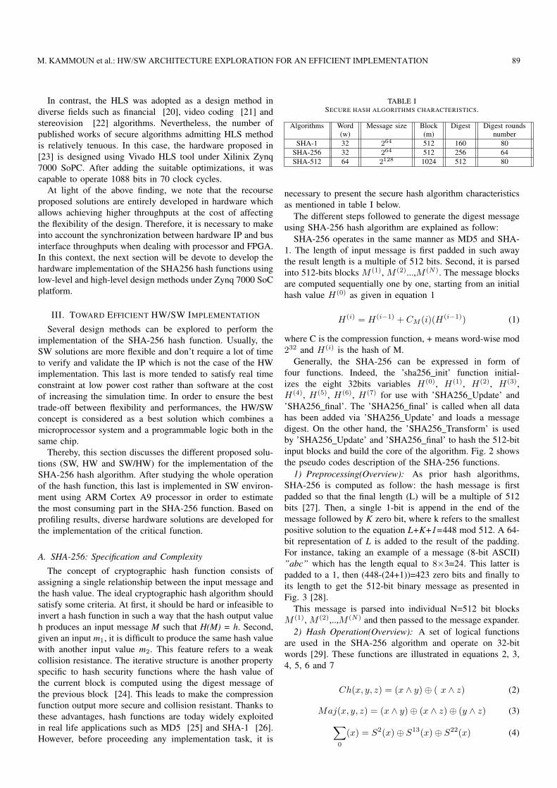
Generally, the SHA-256 can be expressed in form offour functions. Indeed, the ’sha256 init’ function initial-izes the eight 32bits variables H(0), H(1), H(2), H(3),H(4), H(5), H(6), H(7) for use with ’SHA256 Update’ and’SHA256 final’. The ’SHA256 final’ is called when all datahas been added via ’SHA256 Update’ and loads a messagedigest. On the other hand, the ’SHA256 Transform’ is usedby ’SHA256 Update’ and ’SHA256 final’ to hash the 512-bitinput blocks and build the core of the algorithm. Fig. 2 showsthe pseudo codes description of the SHA-256 functions.
1) Preprocessing(Overview): As prior hash algorithms,SHA-256 is computed as follow: the hash message is firstpadded so that the final length (L) will be a multiple of 512bits [27]. Then, a single 1-bit is append in the end of themessage followed by K zero bit, where k refers to the smallestpositive solution to the equation L+K+1=448 mod 512. A 64-bit representation of L is added to the result of the padding.For instance, taking an example of a message (8-bit ASCII)”abc” which has the length equal to 8×3=24. This latter ispadded to a 1, then (448-(24+1))=423 zero bits and finally toits length to get the 512-bit binary message as presented inFig. 3 [28].
This message is parsed into individual N=512 bit blocksM (1), M (2),..,M (N) and then passed to the message expander.
2) Hash Operation(Overview): A set of logical functionsare used in the SHA-256 algorithm and operate on 32-bitwords [29]. These functions are illustrated in equations 2, 3,4, 5, 6 and 7
Ch(x, y, z) = (x ∧ y)⊕ ( x ∧ z) (2)
Maj(x, y, z) = (x ∧ y)⊕ (x ∧ z)⊕ (y ∧ z) (3)∑0
(x) = S2(x)⊕ S13(x)⊕ S22(x) (4)
M. KAMMOUN et al.: HW/SW ARCHITECTURE EXPLORATION FOR AN EFFICIENT IMPLEMENTATION 89
void sha256_update(SHA256_CTX *ctx,const unsigned char data[], size_t len){Unsigned int i;for (i = 0; i < len; ++i) {ctx->data[ctx->datalen] = data[i];ctx->datalen++;if (ctx->datalen == 64) {sha256_transform(ctx, ctx->state, ctx->data,ctx->state);ctx->bitlen += 512;ctx->datalen = 0;
}} }
void sha256_final(SHA256_CTX *ctx, unsigned char hash[]){ unsigned int i;
i = ctx->datalen;// Pad whatever data is left in the buffer.if (ctx->datalen < 56) {
ctx->data[i++] = 0x80;while (i < 56)ctx->data[i++] = 0x00;}
else { ctx->data[i++] = 0x80;while (i < 64)
ctx->data[i++] = 0x00; sha256_transform(ctx,ctx->state, ctx->data,ctx->state); memset(ctx->data, 0, 56);}// Append to the padding the total message's length in bits and transform.ctx->bitlen += ctx->datalen * 8;ctx->data[63] = ctx->bitlen;ctx->data[62] = ctx->bitlen >> 8;ctx->data[61] = ctx->bitlen >> 16;ctx->data[60] = ctx->bitlen >> 24;ctx->data[59] = ctx->bitlen >> 32;ctx->data[58] = ctx->bitlen >> 40;ctx->data[57] = ctx->bitlen >> 48;ctx->data[56] = ctx->bitlen >> 56;sha256_transform(ctx, ctx->state,ctx->data,ctx->state);// Since this implementation uses little endian byte ordering and SHA uses big endian,// reverse all the bytes when copying the final state to the output hash.for (i = 0; i < 4; ++i) {hash[i] = (ctx->state[0] >> (24 - i * 8)) & 0x000000ff;hash[i + 4] = (ctx->state[1] >> (24 - i * 8)) & 0x000000ff;hash[i + 8] = (ctx->state[2] >> (24 - i * 8)) & 0x000000ff;hash[i + 12] = (ctx->state[3] >> (24 - i * 8)) & 0x000000ff;hash[i + 16] = (ctx->state[4] >> (24 - i * 8)) & 0x000000ff;hash[i + 20] = (ctx->state[5] >> (24 - i * 8)) & 0x000000ff;hash[i + 24] = (ctx->state[6] >> (24 - i * 8)) & 0x000000ff;hash[i + 28] = (ctx->state[7] >> (24 - i * 8)) & 0x000000ff;}
}
Fig. 2. Code description of the SHA-256 functions.
01100001 011 00010 01100011 1 00...0 0...011000
423 64
Fig. 3. Preprocessing of the SHA-256.
∑1
(x) = S6(x)⊕ S11(x)⊕ S25(x) (5)
δ0 = S7(x)⊕ S18(x)⊕R3(x) (6)
δ1 = S17(x)⊕ S19(x)⊕R10(x) (7)
where ⊕ , ∧ and ∼ are respectively the bitwise XOR, thebitwise AND and NOT while R and S represent the right shiftand right rotation by n bits.
Fig. 4 illustrates the different steps proceeded in order tohash a message M which contains N blocks: Where Wu isthe expanded message blocks (W0 , W1 , W63) which arecomputed as given in equations 8 and 9, while Ku is asequence of 64 constants used to initialize hash values:
Wu =Mu; (u = 0..15) (8)
For i=1 to N {
1. Initialize a, b, c, d, e, f, g, h variables with the 𝑖 − 1 𝑠𝑡 intermediate hash value.
a← H₀ 𝑖−1
b←H₁ 𝑖−1
h←H₇ 𝑖−1
2. Apply the SHA_256 compression function to update a, b,.....h values.
For u =0 to 63{
Compute Ch(e,f,g), Maj(a,b,c), Ʃₒ(a), Ʃ₁(e), and Wᵤ
T₁ ← h+ Ʃ₁(e) + Ch(e, f, g) + Kᵤ + Wᵤ
T₂ ←Ʃₒ(a) + Maj(a,b,c)
h ← g
g ← f
f ← e
e ← d + T₁
d ← c
c ← b
b ← a
a ← T₁ + T₂
}
3. Compute the 𝑖 𝑡ℎ intermediate hash value H(𝑖)
H₁ 𝑖 ← a + H₀ 𝑖−1
H₂ 𝑖 ← b + H₁ 𝑖−1
H₈ 𝑖 ← h + H₇ 𝑖−1
}
H(𝑁) = (H₀ 𝑁 , H₁ 𝑁 , …… . . H₇ 𝑁 )is the hash of M.
}
Fig. 4. The steps proceeded to hash a message.
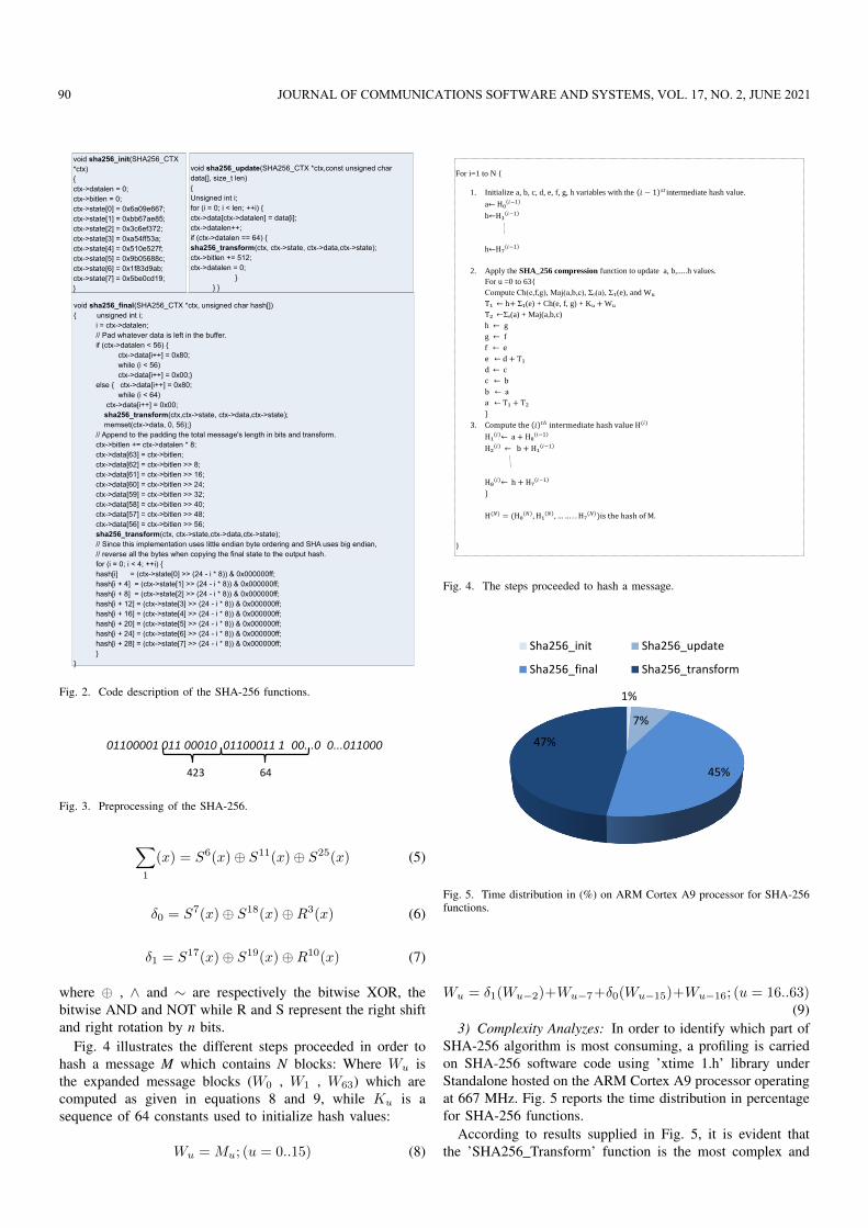
1%
7%
45%
47%
Sha256_init Sha256_update
Sha256_final Sha256_transform
Fig. 5. Time distribution in (%) on ARM Cortex A9 processor for SHA-256functions.
Wu = δ1(Wu−2)+Wu−7+δ0(Wu−15)+Wu−16; (u = 16..63)(9)
3) Complexity Analyzes: In order to identify which part ofSHA-256 algorithm is most consuming, a profiling is carriedon SHA-256 software code using ’xtime 1.h’ library underStandalone hosted on the ARM Cortex A9 processor operatingat 667 MHz. Fig. 5 reports the time distribution in percentagefor SHA-256 functions.
According to results supplied in Fig. 5, it is evident thatthe ’SHA256 Transform’ function is the most complex and
90 JOURNAL OF COMMUNICATIONS SOFTWARE AND SYSTEMS, VOL. 17, NO. 2, JUNE 2021
Hₒ(i)
H₁(i)
H₂(i)
H₃(i)
H₄(i)
H₅(i)
H₆(i)
H₇(i) Dig
es
t M
es
sa
ge
8*3
2b
its
a
b
c
d
e
f
g
h
Intermediate
registers
8*32bits
ROM
to store (Kᵤ)
constant
values
64*32bits
Ch (e,f,g)
Maj (a,b,c)
∑ₒ(a)
∑₁(e)
+T2
+
+
+
T1
+
+
+
Sh
ift
reg
iste
r
Co
mp
ressio
n e
ng
ine
σₒ(wᵤ)
σ₁(wᵤ)w
ᵤ u
nit
wᵤ values64* 32bits
wᵤ
+
Input 1632bits
Input 1532bits
Input 132bits
Input 232bits
512 bits
512 bits
Control unit
Clk rstUp EN
++
8 a
dd
ers
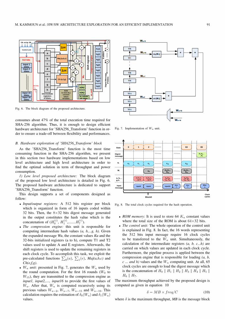
Fig. 6. The block diagram of the proposed architecture.
consumes about 47% of the total execution time required forSHA-256 algorithm. Thus, it is enough to design efficienthardware architecture for ’SHA256 Transform’ function in or-der to ensure a trade-off between flexibility and performances.
B. Hardware exploration of ’SHA256 Transform’ block
As the ’SHA256 Transform’ function is the most timeconsuming function in the SHA-256 algorithm, we presentin this section two hardware implementations based on lowlevel architecture and high level architecture in order tofind the optimal solution in term of throughput and powerconsumption.
1) Low level proposed architecture: The block diagramof the proposed low level architecture is detailed in Fig. 6.The proposed hardware architecture is dedicated to support’SHA256 Transform’ function.
This design supports a set of components designed asfollow:
• Input/output registers: A 512 bits register per blockwhich is organized in form of 16 inputs coded within32 bits. Then, the 8×32 bits digest message generatedin the output constitutes the hash value which is theconcatenation of (H(i)
0 , H(i)1 ,........H(i)
7 ).• The compression engine: this unit is responsible for
computing intermediate hash values (a, b,...g, h). Giventhe expanded message Wu, the constant values Ku and the32-bits initialized registers (a to h), compute T1 and T2values used to update A and E registers. Afterwards, theshift registers is used to update the remaining registers ineach clock cycle. To accomplish this task, we exploit thepre-calculated functions
∑0(a),
∑1(e), Maj(a,b,c) and
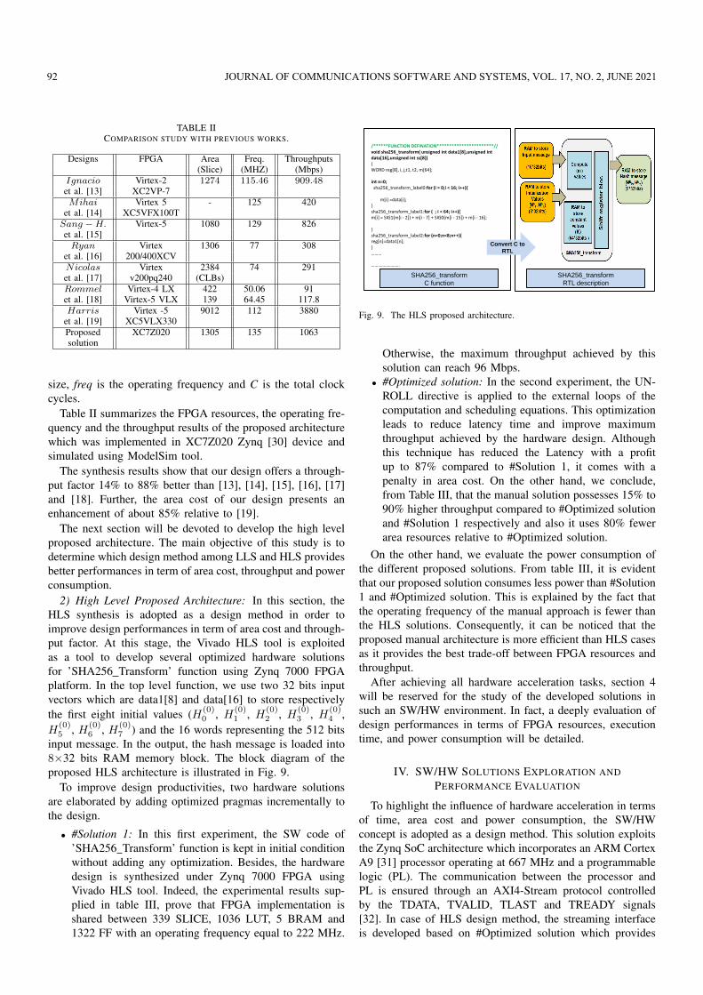
Ch(e,f,g).• Wu unit: presented in Fig. 7, generates the Wu used by
the round computation. For the first 16 rounds (W0 toW15), they are transmitted to the compression engine asinput1, input2,...., input16 to provide the first values ofWu. After that, Wu is computed recursively using itsprevious values Wu−2, Wu−7, Wu−15 and Wu−16. Thiscalculation requires the estimation of δ0(Wu) and δ1(Wu)values.
Fig. 7. Implementation of Wu unit.
input0 input1 input15
0 1 2 63State
Input
message
aₒ,bₒ,cₒ
…gₒ,hₒ
a₁,b₁,c₁…g₁,h₁
a₁₄,b₁₄,c₁₄..,h₁₄
a₆₂,b₆₂,c₆₂..,h₆₂
65
Hₒ,H₁…,H₇
Digest
message
W₀W₀,W₁…
W₁₃W₀,W₁…
W₆₁
K₀ K₁ K₂ K₁₅ K₆₃Kᵢ
Wᵢ
aᵢ, bᵢ,…
gᵢ,hᵢ
Bloc
1
Clock
cyclesBlock0
Bloc
3
Bloc
n
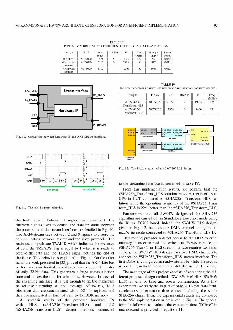
Fig. 8. The total clock cycles required for the hash operation.
• ROM memory: It is used to store 64 Ku constant valueswhere the total size of the ROM is about 64×32 bits.
• The control unit: The whole operation of the control unitis explained in Fig. 8. In fact, the 16 words representingthe 512 bits input message require 16 clock cyclesto be transferred to the Wu unit. Simultaneously, thecalculation of the intermediate registers (a, b, c...h) arecarried on which values are updated in each clock cycle.Furthermore, the pipeline process is applied between thecompression engine that is responsible for loading (a, b,c ... and h) values and the Wu computing unit. At all, 65clock cycles are enough to load the digest message whichis the concatenation of H0 ‖ H1 ‖ H2 ‖ H3 ‖ H4 ‖ H5 ‖H6 ‖ H7.
The maximum throughput achieved by the proposed design iscomputed as given in equation 10
δ =MB × freq/C (10)
where δ is the maximum throughput, MB is the message block
M. KAMMOUN et al.: HW/SW ARCHITECTURE EXPLORATION FOR AN EFFICIENT IMPLEMENTATION 91
TABLE IICOMPARISON STUDY WITH PREVIOUS WORKS.
Designs FPGA Area Freq. Throughputs(Slice) (MHZ) (Mbps)
et al. [19] XC5VLX330Proposed XC7Z020 1305 135 1063solution
size, freq is the operating frequency and C is the total clockcycles.
Table II summarizes the FPGA resources, the operating fre-quency and the throughput results of the proposed architecturewhich was implemented in XC7Z020 Zynq [30] device andsimulated using ModelSim tool.
The synthesis results show that our design offers a through-put factor 14% to 88% better than [13], [14], [15], [16], [17]and [18]. Further, the area cost of our design presents anenhancement of about 85% relative to [19].
The next section will be devoted to develop the high levelproposed architecture. The main objective of this study is todetermine which design method among LLS and HLS providesbetter performances in term of area cost, throughput and powerconsumption.
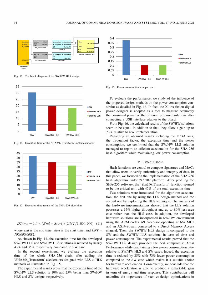
2) High Level Proposed Architecture: In this section, theHLS synthesis is adopted as a design method in order toimprove design performances in term of area cost and through-put factor. At this stage, the Vivado HLS tool is exploitedas a tool to develop several optimized hardware solutionsfor ’SHA256 Transform’ function using Zynq 7000 FPGAplatform. In the top level function, we use two 32 bits inputvectors which are data1[8] and data[16] to store respectivelythe first eight initial values (H(0)
0 , H(0)1 , H(0)
2 , H(0)3 , H(0)
4 ,H
(0)5 , H(0)
6 , H(0)7 ) and the 16 words representing the 512 bits
input message. In the output, the hash message is loaded into8×32 bits RAM memory block. The block diagram of theproposed HLS architecture is illustrated in Fig. 9.
To improve design productivities, two hardware solutionsare elaborated by adding optimized pragmas incrementally tothe design.
• #Solution 1: In this first experiment, the SW code of’SHA256 Transform’ function is kept in initial conditionwithout adding any optimization. Besides, the hardwaredesign is synthesized under Zynq 7000 FPGA usingVivado HLS tool. Indeed, the experimental results sup-plied in table III, prove that FPGA implementation isshared between 339 SLICE, 1036 LUT, 5 BRAM and1322 FF with an operating frequency equal to 222 MHz.
Convert C to
RTL
SHA256_transform
C function
SHA256_transform
RTL description
/******FUNCTION DEFINATION***********************//void sha256_transform( unsigned int data1[8],unsigned intdata[16],unsigned int ss[8]){WORD reg[8], i, j,t1, t2, m[64];
int n=0;sha256_transform_label0:for (i = 0;i < 16; i++){
Otherwise, the maximum throughput achieved by thissolution can reach 96 Mbps.
• #Optimized solution: In the second experiment, the UN-ROLL directive is applied to the external loops of thecomputation and scheduling equations. This optimizationleads to reduce latency time and improve maximumthroughput achieved by the hardware design. Althoughthis technique has reduced the Latency with a profitup to 87% compared to #Solution 1, it comes with apenalty in area cost. On the other hand, we conclude,from Table III, that the manual solution possesses 15% to90% higher throughput compared to #Optimized solutionand #Solution 1 respectively and also it uses 80% fewerarea resources relative to #Optimized solution.
On the other hand, we evaluate the power consumption ofthe different proposed solutions. From table III, it is evidentthat our proposed solution consumes less power than #Solution1 and #Optimized solution. This is explained by the fact thatthe operating frequency of the manual approach is fewer thanthe HLS solutions. Consequently, it can be noticed that theproposed manual architecture is more efficient than HLS casesas it provides the best trade-off between FPGA resources andthroughput.
After achieving all hardware acceleration tasks, section 4will be reserved for the study of the developed solutions insuch an SW/HW environment. In fact, a deeply evaluation ofdesign performances in terms of FPGA resources, executiontime, and power consumption will be detailed.
IV. SW/HW SOLUTIONS EXPLORATION ANDPERFORMANCE EVALUATION
To highlight the influence of hardware acceleration in termsof time, area cost and power consumption, the SW/HWconcept is adopted as a design method. This solution exploitsthe Zynq SoC architecture which incorporates an ARM CortexA9 [31] processor operating at 667 MHz and a programmablelogic (PL). The communication between the processor andPL is ensured through an AXI4-Stream protocol controlledby the TDATA, TVALID, TLAST and TREADY signals[32]. In case of HLS design method, the streaming interfaceis developed based on #Optimized solution which provides
92 JOURNAL OF COMMUNICATIONS SOFTWARE AND SYSTEMS, VOL. 17, NO. 2, JUNE 2021
TABLE IIIIMPLEMENTATION RESULTS OF THE HLS SOLUTIONS UNDER FPGA PLATFORM.
Fig. 10. Connection between hardware IP and AX4-Stream interface.
Fig. 11. The AXI4-stream behavior.
the best trade-off between throughput and area cost. Thedifferent signals used to control the transfer status betweenthe processor and the stream interfaces are detailed in Fig. 10.The AXI4-stream uses between 2 and 9 signals to ensure thecommunication between master and the slave protocols. Themain used signals are TVALID which indicates the presenceof data, the TREADY flag is equal to 1 when it is ready toreceive the data and the TLAST signal notifies the end ofthe frame. This behavior is explained in Fig. 11. On the otherhand, the work presented in [33] proved that the AXI4-Lite busperformances are limited since it provides a sequential transferof only 32-bit data. This generates a huge communicationtime and makes the transfer a bit slow. However, In case ofthe streaming interface, it is just enough to fix the maximumpacket size depending on input message. Afterwards, the 8bits input data are concatenated within 32 bits registers andthen communicated in form of train to the DDR memory.
A synthesis results of the proposed hardware IPswith HLS (#SHA256 Transform HLS) and LLS(#SHA256 Transform LLS) design methods connected
TABLE IVIMPLEMENTATION RESULTS OF THE PROPOSED STREAMING INTERFACES.
Fig. 12. The block diagram of the SW/HW LLS design.
to the streaming interface is presented in table IV.From this implementation results, we confirm that the
#SHA256 Transform LLS solution provides a gain of about84% in LUT compared to #SHA256 Transform HLS so-lution while the operating frequency of the #SHA256 Transform HLS is 22% better than the #SHA256 Transform LLS.
Furthermore, the full SW/HW designs of the SHA-256algorithm are carried out in Standalone execution mode usingthe Xilinx ZC702 board. Indeed, the SW/HW LLS design,given in Fig. 12, includes one DMA channel configured inread/write mode connected to #SHA256 Transform LLS IP.
This routing provides a direct access to the DDR externalmemory in order to read and write data. However, since the#SHA256 Transform HLS stream interface requires two inputvectors, the SW/HW HLS design uses two DMA channels toconnect the #SHA256 Transform HLS stream interface. Thefirst DMA is configured in read/write mode while the secondis operating in write mode only as detailed in Fig. 13 below.
The next stage of this project consists of comparing the dif-ferent proposed design methods (SW, SW/HW HLS, SW/HWLLS) in term of time and power consumption. As a firstexperiment, we study the impact of only ’SHA256 transform’accelerators on execution time without including the wholeSHA-256 chain. Then, the experimental results are comparedto the SW implementation as presented in Fig. 14. The generalformula followed to evaluate the execution time ”DTime” inmicrosecond is provided in equation 11:
M. KAMMOUN et al.: HW/SW ARCHITECTURE EXPLORATION FOR AN EFFICIENT IMPLEMENTATION 93
S_AXIS_S2MMM_AXI_MM2S
M_AXI_S2MM M_AXIS_MM2S
CLKRST
S_AXI_LITE
M_AXI_MM2S M_AXIS_MM2S
CLK
RST S_AXI_LITE
DataM0_TDATA
S_AXI_LITE
CLK
RST
INTERRUPT
SHA256_Transform_HLS
S00_AXI
S01_AXI
M00_AXI
CLKRST
AXI_Interconnect 0
S00_AXIM00_AXI
CLKRST
AXI_Interconnect 1
CLKRST
S_AXI_HP0
S_AXI_HP1
M_AXI_GP0
AXI DMA0
AXI DMA1INTERRUPT
Data1
Processing
system
Fig. 13. The block diagram of the SW/HW HLS design.
0
5
10
15
20
25
30
35
SW SW/HW HLS SW/HW LLS
SW
SW/HW HLS
SW/HW LLS
Fig. 14. Execution time of the SHA256 Transform implementations.
0
5
10
15
20
25
30
35
40
45
SW SW/HW HLS SW/HW LLS
SW
SW/HW HLS
SW/HW LLS
Fig. 15. Execution time results of the SHA-256 algorithm.
DTime = 1.0× (End− Start)/(CNT/1, 000, 000) (11)
where end is the end time, start is the start time, and CNT =100,000,000/2.
As shown in Fig. 14, the execution time for the developedSW/HW LLS and SW/HW HLS solutions is reduced by nearly43% and 35% respectively compared to SW case.
In the second experiment, we evaluate the executiontime of the whole SHA-256 chain after adding the’SHA256 Transform’ accelerators designed with LLS et HLSmethods as illustrated in Fig. 15.
The experimental results prove that the execution time of theSW/HW LLS solution is 10% and 25% better than SW/HWHLS and SW designs respectively.
0
0,05
0,1
0,15
0,2
0,25
0,3
0,35
0,4
SW SW/HW HLS SW/HW LLS
SW
SW/HW HLS
SW/HW LLS
Fig. 16. Power consumption comparison.
To evaluate the performance, we study of the influence ofthe proposed design methods on the power consumption con-straint as detailed in Fig. 16. In fact, the Xilinx fusion digitalpower designer is adopted as a tool to measure accuratelythe consumed power of the different proposed solutions afterconnecting a USB interface adapter to the board.
From Fig. 16, the calculated results of the SW/HW solutionsseem to be equal. In addition to that, they allow a gain up to73% relative to SW implementation.
Regarding all obtained results including the FPGA area,the throughput factor, the execution time and the powerconsumption, we confirmed that the SW/HW LLS solutionmanaged to report an efficient acceleration for the SHA-256hash algorithm while maintaining low power consumption.
V. CONCLUSION
Hash functions are central to compute signatures and MACsthat allow users to verify authenticity and integrity of data. Inthis paper, we focused on the implementation of the SHA-256hash algorithm under ZC 702 platform. After profiling theSHA-256 software, the ’Sha256 Transform’ function seemedto be the critical unit with 47% of the total execution time.
Two solutions were introduced for the algorithm accelera-tion, the first one by using the LLS design method and thesecond one by exploiting the HLS technique. The analysis ofthe hardware implementations showed that the LLS solutionpossesses a 15% higher throughput and up to 80% less areacost rather than the HLS case. In addition, the developedhardware solutions are incorporated in SW/HW environmentusing the ARM cortex A9 processor operating at 667 MHzand an AXI4-Stream connected to a Direct Memory Accesschannel. Then, the SW/HW HLS design is compared to theSW and the SW/HW LLS solutions in term of time andpower consumption. The experimental results proved that theSW/HW LLS design provided the best compromise Area/Performance while maintaining a low power consumption ratiorelative to SW/HW HLS and SW cases. Indeed, the executiontime is reduced by 25% with 73% lower power consumptioncompared to the SW case which makes it a suitable choicefor hardware acceleration. Consequently, we conclude that thehardware acceleration is able to produce a remarkable gainin term of energy and time response. This contribution willunderline the importance of such co-design optimizations in
94 JOURNAL OF COMMUNICATIONS SOFTWARE AND SYSTEMS, VOL. 17, NO. 2, JUNE 2021
order to improve the embedded system architecture across thetraditional boundaries of hardware and software. Also, it letsthe developers to think about design in terms of a trade-offbetween performance and flexibility.
Although the amelioration performed by our work, theresults still average, which push us to think of better way tooptimize the accelerator to cost less resource. As future works,we will migrate to a more sophisticated processor from RISC-V to have better results. In addition to that, we will studyother recent hash algorithms using HW/SW design methodin order to estimate implementation constraints and compareresults with the SHA-256 proposed solution. Furthermore, wecan also exploit reconfigurable methods as a solution to avoidmemory overhead and decrease power consumption.
REFERENCES
[1] A. Ben Atitallah,M. Kammoun, An FPGA comparative study of high-level and low-level combined designs for HEVC intra, inverse quantiza-tion, and IDCT/IDST 2D modules, international journal of circuit theoryand applications, 1-17,2020, https://doi.org/10.1002/cta.2790.
[2] S. Lahti, P. Sjvall, Are we there yet? A study on the stateof high-level synthesis, IEEE Transactions on Computer-Aided De-sign of Integrated Circuits and Systems, 38(5):898-911, 2019, DOI:10.1109/TCAD.2018.2834439.
[3] M. Pelcat, C. Bourrasset, Design productivity of a high-level syn-thesis compiler versus HDL, IEEE SAMOS’16, 17-21, 2016, DOI :10.1109/SAMOS.2016.7818341.
[4] P. Sjvall, High-level synthesis of HEVC intra prediction on FPGA, Masterof Science Thesis, 2015.
[5] X.S. Zhang, Tutorial for Vivado HLS. Washington University, St. Louis,Missouri, https: //www.ese.wustl.edu/ xuan.zhang/ ese566files/ tutori-als/.pdf, 2007.
[6] CALYPTO, Catapult C Synthesis. http://www.calypto.com/catapult-c-synthesis.php.
[7] M. Elleuchi , M. Boujelben, Towards low power security mechanismsand architectures for Wireless Sensor Networks. Journal of InformationAssurance and Security, 13: 066-079, 2018.
[8] T. Dipti, and M. Utsav Kumar, Low Power Implementation of Se-cure Hashing Algorithm (SHA-2) using VHDL on FPGA of SHA-256,International Journal for Research in Applied Science & EngineeringTechnology, 13(5), (2018), DOI: 10.22214/ijraset.2018.5376.
[9] National Institute of Standards and Technology, Secure Hash Standard.Federal information Processing Standards, 180-4, 2012.
[10] Z. Xiaoyong , W. Ruizhen . A High-Performance Parallel ComputationHardware Architecture in ASIC of SHA-256 Hash. International Confer-ence on Advanced Communications Technology(ICACT), 17-20, 2019,DOI: 10.23919/ICACT48636.2020.9061457.
[11] K.T. Kurt, C.L.Y. Steve, An FPGA based SHA-256 processor. Interna-tional Conference on Field Programmable Logic and Applications, 577-585, 2012, DOI: https://doi.org/10.1007/3-540-46117-5 60.
[12] Xilinx, Inc. ZC-702 Evaluation Board for the Zynq-7000 XC7Z020 All Programmable SoC. (Available from:http://www.xilinx.com/support/documentation/boards and kits/zc702zvik/ug850-zc702-eval-bd.pdf).
[13] I. Algredo-Badilloa, C. Feregrino-Uribe, FPGA-based implementa-tion alternatives for the inner loop of the Secure Hash AlgorithmSHA-256, Microprocessors and Microsystems, 37: 750-757, 2013,https://doi.org/10.1016/j.micpro.2012.06.007.
[14] T. Mihai, F. Adrian, Design and implementation of cryptographic mod-ules on FPGAs. Proceedings of the Applied Mathematics and Informatics,2010, 149154, 2010.
[15] L. Sang-Hyun, S. Kyung-Wook, An Efficient Implementation ofSHA processor including three Hash Algorithms (SHA-512, SHA-512/224, SHA-512/256). International Conference on Electronics, In-formation, and Communication, 24-27, 2018, DOI: 10.23919/ELINFO-COM.2018.8330578.
[16] G. Ryan, I. Laurent, Multi-mode operator for SHA-2 hashfunctions. Journal of Systems Architecture, 53: 127-138, 2007,https://doi.org/10.1016/j.sysarc.2006.09.006.
[17] N. Sklavos, and O. Koufopavlou, Implementation of the SHA-2 HashFamily Standard Using FPGAs. The Journal of Supercomputing, 31: 227-248, 2005, https://doi.org/10.1007/s11227-005-0086-5.
[18] G. Rommel, , A. Ignacio, A compact FPGA-based processor for theSecure Hash Algorithm SHA-256, Computers and Electrical Engineering,40: 194-202, 2014, https://doi.org/10.1016/j.compeleceng.2013.11.014.
[19] E.M. Harris , K. Apostolis, Hardware Implementation of the Totally Self-Checking SHA-256 Hash Core, International Conference on Computer asa Tool (EUROCON), 2015, DOI: 10.1109/EUROCON.2015.7313715.
[20] I. Gordon, F. Shane, Is high level synthesis ready for business a com-putational finance case study, in Int. Conf. Field-Programmable Technol.(FPT), 2014, DOI: 10.1109/FPT.2014.7082747.
[21] M. Kammoun, , B.A. Ahmed, Case study of an HEVC decoder ap-plication using high-level synthesis: intra prediction, dequantization, andinverse transform blocks, Journal of Electronic Imaging, 28, 2019, DOI:10.1117/1.JEI.28.3.033010.
[22] A. Karim, B.A. Rabie, Exploring HLS optimizations for efficient stereomatching hardware implementation. in Int. Symp. Appl. ReconfigurableComput., 168-176, 2017, DOI: 10.1007/978-3-319-56258-2.
[23] H S. Jacinto, L. Daoud , High Level Synthesis Using Vivado HLSfor Optimizations of SHA-3. 60th International Midwest Symposiumon Circuits and Systems (MWS-CAS), 6-9, 2017, DOI: 10.1109/MWS-CAS.2017.8052985.
[24] A. Imtiaz, A. Shoba Das, Hardware implementation analysis of SHA-256 and SHA-512 algorithms on FPGAs, Computers and ElectricalEngineering, 31: 345-360, 2005, https://doi.org/ 10.1016/ j.compeleceng.2005.07.001.
[25] A. Radwa, M.M. Fouad, Design and implementation of new securityhash algorithm based on MD5 and SHA-256. International Journal ofEngineering Sciences &Emerging Technologies, 6: 29-36, 2013.
[26] W. Xiaoyun , L Y. Yiqun, Finding collisions in the full SHA-1, in: V.Shoup (Ed.), Advances in Cryptology CRYPTO’05, 3621: 17-36, 2005,DOI https://doi.org/10.1007/11535218 2.
[27] IWS, Descriptions of SHA-256, SHA-384, and SHA-512.http://www.iwar.org.uk/comsec/resources/cipher/sha256-384-512.pdf.
[28] K. Fatma , M. Hassen, Efficient FPGA hardware implementation ofsecure hash function SHA-256/Blacke-256, 12th International Multi-Conference on Systems, Signals & Devices (SSD15), 2015, DOI:10.1109/SSD.2015.7348105.
[29] D. Rachmawati, J T. Tarigan, A comparative study of Message Digest5(MD5) and SHA256 algorithm. 2nd International Conference on Com-puting and Applied Informatics, 2017.
[33] M. Kammoun, A. Ben Atitallah, Design exploration of effcient imple-mentation on SoC heterogeneous platform. International Journal of CircuitTheory and Applications, 45: 2243-2259, 2016, DOI : 10.1002/cta.2308.
M. KAMMOUN et al.: HW/SW ARCHITECTURE EXPLORATION FOR AN EFFICIENT IMPLEMENTATION 95
Manel Elleuchi was born in 1985. Currently, sheis a Doctor at the National Engineering Schoolof Sfax. Her research activity is conducted withinCES research unit. She has received a Ph.D. incomputer systems engineering in December 2017.She has received the Engineering degree, from theNational School of Engineers of Sfax (ENIS), Tunis,Tunisia in 2009 and the Master degree in NewTechnologies of Dedicated Computer Systems, fromthe National Engineering School of Sfax, in 2012.She has authored more than 10 papers. Her current
research interests are in the field of Wireless Sensor Networks (WSNs) andthe Internet of things (IoT). She focused on the security and routing protocolsin WSNs and IoT in low power consumption.
Mohamed Abid is head of Computer EmbeddedSystem laboratory CES-ENIS, Tunisia. He is work-ing now as a Professor at the Engineering NationalSchool of Sfax (ENIS), University of Sfax, TunisiaHe received the Ph. D. degree from the NationalInstitute of Applied Sciences, Toulouse (France)in 1989 in the area of Computer Engineering &Microelectronics. His current research interests in-clude: hardware-software codesign, System on Chip,Reconfigurable System, and Embedded System, etc.He has also been investigating the design and im-
plementation issues of FPGA embedded systems. Dr. Abid served in nationalor international conference organization and program committees at differ-ent organizational levels including Conference CoGeneral Chair, Technicalprogram co-chair, organization co-chair and Member of several national andinternational conference Program Committees. He was Founding Member ofseveral international conferences and school: SCS, SSD, GEI, and Sensor NetSchool. Recently, he is Vice General Co-chair of IDT’10. He was GeneralCo-chair of SensorNetSchool’09, Vice General Co-chair of IDT’09, andSpecial Session Co-chair of ICECS’09. He is Member of technical committeeof DASIP since 2007, ICM 2010 since 2006, ComNet 2010, and GeneralCo-chair of IDT’08. He was also Joint Editor of Specific Issues in twoInternational Journals and Joint editor of many conference’s articles nationalsand internationals: ICM’2004, GEI’2006-07, SCS’2004. He is a co-editor ofthe best paper in the international conference EDAC-ETC-EuroASIC’96.
Abdulfattah M. Obeid is deputy Director for Scien-tific Affairs, National Center for Electronics, Com-munications and Photonics at KACST. Founded andleading the Advanced Microsensors Division of ECPthat is charged with stimulating the developmentof microelectronic development in the Kingdom ofSaudi Arabia through provision of low cost manu-facturing services in the region. Formed long-termstrategic partnerships with a number of internationalprivate and public organizations and institutions forthe implementation of various projects of national
importance. He was a key member (Coordinator of the Electronics, Communi-cations and Photonics strategic technology) of the implementation committeethat drafted and the National Science, Technology and Innovation plan forSaudi Arabia. His research interests are Reconfigurable computing, VLSIarchitectures for DSP, Computer architecture, Wireless sensor networks andMEMS.
Manel Kammoun received her PhD in electron-ics from the National School of Engineering-Sfax(ENIS) in 2018 and her diploma of engineer inelectronics from the University of Sfax in 2012.Currently, she is researcher in the Laboratory ofElectronics and Information Technology within theC&S (Circuit & System) team. Her main researchactivities are focused on image and video signalprocessing, hardware implementation, and embed-ded systems.
96 JOURNAL OF COMMUNICATIONS SOFTWARE AND SYSTEMS, VOL. 17, NO. 2, JUNE 2021


![Verifying HW/SW Integration - T&VS HW/SW Integration ... faults) • Soft Errors – Transients ... (DAC), June 10-14, 2002, New Orleans, Louisiana, USA.]](https://static.documents.pub/doc/80x56/5b027ecf7f8b9a89598faeb5/verifying-hwsw-integration-hwsw-integration-faults-soft-errors-.jpg)


