I. Device fabrication The devices supporting asymmetric optical power transmission (Fig. 3(b)) were fabricated using the following procedure. A 4-m SiO2 film was deposited onto a Si substrate using plasma-enhanced chemical vapor deposition (PECVD). A 1.4-m SiN film was then deposited onto the as-prepared SiO2/Si wafer using low-pressure chemical vapor deposition (LPCVD). The composition and thickness of the SiN film were determined using energy-dispersive X-ray spectroscopy (EDX). This wafer was then rinsed and cleaned using Acetone, IPA, and DI water, followed by oxygen plasma treatment for 5 min. After that, double layers of polymethyl methacrylate (PMMA) electron-beam resist (i.e., 495K PMMA A4 and 950K PMMA A2) were spun onto the wafer and the wafer was baked at 180oC for 5 minutes for the first PMMA layer and for 3 minutes for the second PMMA layer. The phased antenna arrays as well as the alignment marks were patterned using electron-beam lithography (i.e., electron-beam exposure using JEOL6300-FX at a beam current of 250 pA, development in an IPA and DI water mixture solution at 4oC, metallization by electron-beam deposition of 3-nm Cr and 50-nm Au films, and lift-off using two baths of Microposit Remover 1165 at 80oC overnight).
A second electron-beam lithography step was conducted to pattern the waveguides. Double layers of PMMA (i.e., 495K PMMA A6 and 950K PMMA A2) were used as the electron-beam resist. In addition, a layer of Espacer 300Z was spun onto the top of the wafer to prevent strong charging effects during electron-beam exposure. Y-branch waveguides were defined using aligned exposure at a beam current of 4 nA. The wafer was then rinsed in DI water to get rid of the Espacer layer, and developed in an IPA and DI water mixture at 4oC. After the development, a 100-nm Cr film was deposited onto the wafer using electron-beam evaporation, followed by overnight lift-off in Microposit Remover 1165 at 75oC. The wafer was descummed using oxygen plasma at 20oC for 15 seconds to remove electron-beam resist residues. The Cr pattern served as an etch mask and waveguides were etched into the SiN film using inductively coupled plasma reactive-ion etching (ICP-RIE) (i.e., 6 sccm Ar, 55 sccm H2, 40 sccm CF4, 15 mTorr chamber pressure, 125 W RF power, 600 W ICP power, 7.5 minutes). The Cr mask was removed using wet etching (i.e., Transene Cr etchant 1020 at room temperature for 14 minutes). Finally, the wafer was cleaved to form input and output waveguide ports.
The mid-infrared waveguide mode converters shown in Fig. 5 were fabricated using a combination of PECVD, electron-beam lithography, RIE, and electron-beam deposition. A 0.75-m amorphous silicon (a-Si) film was deposited by PECVD on a silicon wafer with 5-m thick thermally grown SiO2. Double layers of PMMA (i.e., 495K PMMA A4 and 950K PMMA A2) were spun onto the wafer and the wafer was baked at 170 °C for 10 minutes for the first PMMA layer and for 2 minutes for the second PMMA layer. Electron-beam lithography (i.e., electron-beam exposure using JEOL6300-FX at a beam current of 1 nA) was used to pattern gold antenna arrays and alignment markers with a development in an IPA and DI water mixture solution (3:1)
for 2 minutes at 4 °C, followed by electron-beam deposition of 3-nm Cr and 50-nm Au films, and a standard overnight lift-off procedure in Acetone. A second electron-beam lithography step was used to create PMMA etch masks to define waveguides. A single layer of PMMA (i.e., 400-nm 950K PMMA A6) was spun onto the wafer and the wafer was baked at 170 °C for 15 minutes. Electron-beam lithography (i.e., electron-beam exposure using a NanoBeam e-Beam writer at a beam current of 1 nA for the grating coupler and 4 nA for the waveguides) was conducted with care using alignment marks to make sure that the antenna arrays and the waveguide etch masks were precisely aligned. The same mixture of IPA and DI water was used for the development. The waveguides were etched into the Si film using RIE (i.e., 18 sccm O2, 40 sccm SF6, 15 W RF power, 800 W ICP power, 37 seconds) after oxygen plasma cleaning (i.e., 50 sccm O2, 50 W RF power, and 800 W ICP power at 30 mTorr and 20 °C for 15 seconds). The PMMA etch masks were removed using Acetone. The wafer was cleaved to form output waveguide ports for far-field measurements.
The telecom waveguide mode converters shown in Fig. 6 were fabricated using the following procedure. X-cut lithium niobate on insulator (LNOI) wafers obtained from NANOLN, with a 400-nm lithium niobate layer bonded on top of a 2-µm SiO2 buffer layer, were used for device fabrication. A 600-nm hydrogen silsesquioxane (HSQ) resist layer was spun on the wafer and patterned with electron-beam lithography. The patterned HSQ was subsequently used as an etch mask to define lithium niobate ridge waveguides using an optimized Ar+ plasma etching, as is described in C. Wang et al. Opt. Express 22, 30924-30933 (2014). The fabricated ridge waveguides for the TE00-to-TM00 mode converters have a top width of 0.95 µm and a ridge height of 250 nm, leaving a 150-nm lithium niobate slab underneath the waveguides. The side walls of the waveguides as a result of the plasma etching have a tilting angle of 40 degrees with respect to the normal of the waveguide top surfaces. The residual HSQ was removed in buffered oxide etch (BOE). A 75-nm p-doped a-Si layer was subsequently deposited on the etched surface using PECVD. With the help of alignment marks, a 300-nm HSQ resist layer was then patterned on the a-Si layer on the waveguide top surfaces using electron-beam lithography. Reactive ion etching was conducted to transfer the second HSQ pattern into the a-Si layer. A second BOE etch was used to remove the residual HSQ resist. The fabricated waveguides and a-Si nano-antennas were cladded in a 3-µm SiO2 layer using PECVD. Finally, waveguide facets were diced and polished to ensure reliable and repeatable optical coupling efficiencies.
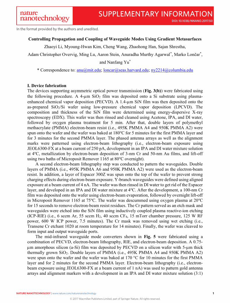
II. Device layout and characterization II.1 Devices supporting asymmetric optical power transmission The devices supporting asymmetric optical power transmission consist of Y-branch waveguides, with a distance of 500 m between two output ports. The phased antenna arrays with opposite orientations were fabricated on top of the two waveguide branches with a width of 2.5 m. The input port was tapered from a width of 10 m to 2.5 m; the two output ports were tapered from 2.5 m to 10 m. Both input and output ports were cleaved. Figure S1 shows additional SEM images of fabricated devices.
Fig. S1 SEM images of a device that supports asymmetric optical power transmission in waveguides. a, Tapered waveguide close to the input port. b, Top view of the Y-junction. c, Perspective view of the Y-junction. d, Two branches from the Y-junction. e and f, Two phased antenna arrays patterned on the two branches.
A schematic of the experimental setup used to characterize the devices supporting asymmetric optical power transmission is shown in Fig. S2. The light source is a broadly tunable laser (Firefly-IR, M Squared Lasers, = 2.5-3.8 μm, 5 nm linewidth), which is coupled to a ZrF4 mid-infrared single-mode fiber. The polarization of the light coming out of the fiber can be controlled by a fiber coupler. Light was coupled from the fiber into the input port of the devices via butt coupling. A mid-infrared camera was used to image the optical spots at the two output ports of the devices. A
wire-grid polarizer was placed in front of the camera to control the polarization of the light that enters the camera.
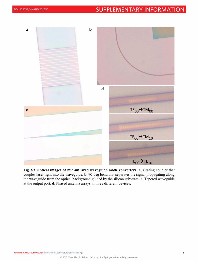
Fig. S2 Schematic of the experimental setup used to characterize the performance of the devices supporting asymmetric optical power transmission in waveguides. The probe light is coupled from a mid-infrared laser into a mid-infrared fiber and then into the sample. The optical spots at the output ports of the devices are captured by a mid-infrared camera. The polarizer is used to control the polarization of the light that enters the camera. Here, A. M. and C. L. represent alignment microscope and convex lens, respectively. II.2 Mid-infrared waveguide mode converters Each of the waveguide mode converters consists of a grating coupler, a waveguide taper, a narrowed segment of waveguide for purifying the TE fundamental waveguide mode, a 90-degree waveguide turn, a segment of waveguide patterned with a phased antenna array, a second waveguide taper, and a cleaved facet for light out-coupling. The entire device is 7-10 mm in length. Figure S3 shows optical images of the waveguide mode converters. High-resolution SEM images of the devices are shown in Fig. S4.
Fig. S3 Optical images of mid-infrared waveguide mode converters. a, Grating coupler that couples laser light into the waveguide. b, 90-deg bend that separates the signal propagating along the waveguide from the optical background guided by the silicon substrate. c, Tapered waveguide at the output port. d, Phased antenna arrays in three different devices.
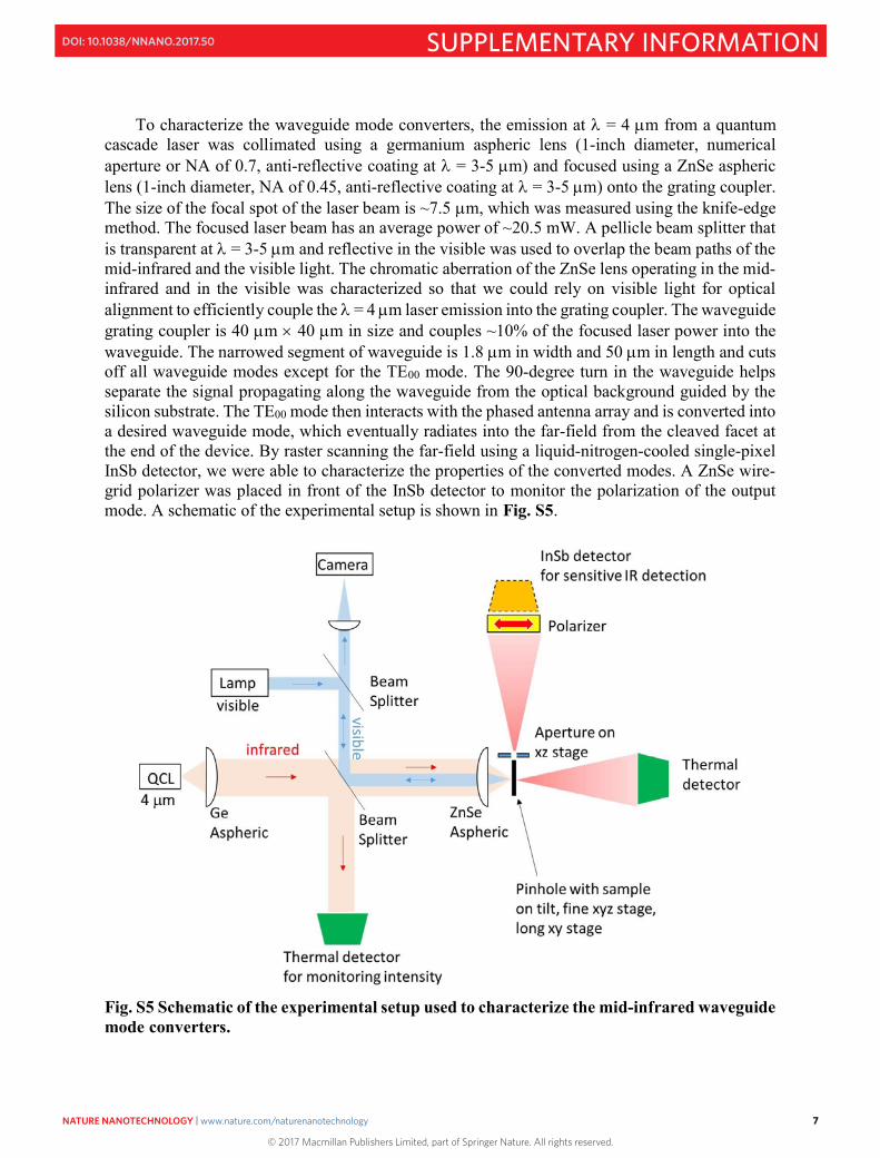
To characterize the waveguide mode converters, the emission at = 4 m from a quantum cascade laser was collimated using a germanium aspheric lens (1-inch diameter, numerical aperture or NA of 0.7, anti-reflective coating at = 3-5 m) and focused using a ZnSe aspheric lens (1-inch diameter, NA of 0.45, anti-reflective coating at = 3-5 m) onto the grating coupler. The size of the focal spot of the laser beam is ~7.5 m, which was measured using the knife-edge method. The focused laser beam has an average power of ~20.5 mW. A pellicle beam splitter that is transparent at = 3-5 m and reflective in the visible was used to overlap the beam paths of the mid-infrared and the visible light. The chromatic aberration of the ZnSe lens operating in the mid-infrared and in the visible was characterized so that we could rely on visible light for optical alignment to efficiently couple the = 4 m laser emission into the grating coupler. The waveguide grating coupler is 40 m 40 m in size and couples ~10% of the focused laser power into the waveguide. The narrowed segment of waveguide is 1.8 m in width and 50 m in length and cuts off all waveguide modes except for the TE00 mode. The 90-degree turn in the waveguide helps separate the signal propagating along the waveguide from the optical background guided by the silicon substrate. The TE00 mode then interacts with the phased antenna array and is converted into a desired waveguide mode, which eventually radiates into the far-field from the cleaved facet at the end of the device. By raster scanning the far-field using a liquid-nitrogen-cooled single-pixel InSb detector, we were able to characterize the properties of the converted modes. A ZnSe wire-grid polarizer was placed in front of the InSb detector to monitor the polarization of the output mode. A schematic of the experimental setup is shown in Fig. S5.
Fig. S5 Schematic of the experimental setup used to characterize the mid-infrared waveguide mode converters.
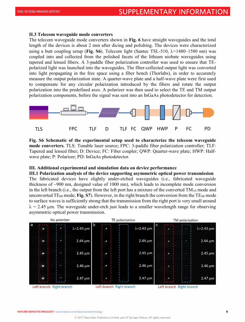
II.3 Telecom waveguide mode converters The telecom waveguide mode converters shown in Fig. 6 have straight waveguides and the total length of the devices is about 2 mm after dicing and polishing. The devices were characterized using a butt coupling setup (Fig. S6). Telecom light (Santec TSL-510, =1480–1580 nm) was coupled into and collected from the polished facets of the lithium niobate waveguides using tapered and lensed fibers. A 3-paddle fiber polarization controller was used to ensure that TE-polarized light was launched into the waveguides. The fiber-collected output light was converted into light propagating in the free space using a fiber bench (Thorlabs), in order to accurately measure the output polarization state. A quarter-wave plate and a half-wave plate were first used to compensate for any circular polarization introduced by the fibers and rotate the output polarization into the predefined axes. A polarizer was then used to select the TE and TM output polarization components, before the signal was sent into an InGaAs photodetector for detection.
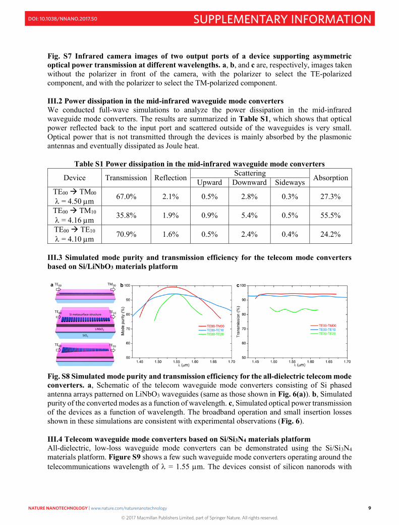
Fig. S6 Schematic of the experimental setup used to characterize the telecom waveguide mode converters. TLS: Tunable laser source; FPC: 3-paddle fiber polarization controller; TLF: Tapered and lensed fiber; D: Device; FC: Fiber coupler; QWP: Quarter-wave plate; HWP: Half-wave plate; P: Polarizer; PD: InGaAs photodetector. III. Additional experimental and simulation data on device performance III.1 Polarization analysis of the device supporting asymmetric optical power transmission The fabricated devices have slightly under-etched waveguides (i.e., fabricated waveguide thickness of ~900 nm, designed value of 1000 nm), which leads to incomplete mode conversion in the left branch (i.e., the output from the left port has a mixture of the converted TM10 mode and unconverted TE00 mode; Fig. S7). However, in the right branch the conversion from the TE00 mode to surface waves is sufficiently strong that the transmission from the right port is very small around = 2.45 m. The waveguide under-etch just leads to a smaller wavelength range for observing asymmetric optical power transmission.
Fig. S7 Infrared camera images of two output ports of a device supporting asymmetric optical power transmission at different wavelengths. a, b, and c are, respectively, images taken without the polarizer in front of the camera, with the polarizer to select the TE-polarized component, and with the polarizer to select the TM-polarized component. III.2 Power dissipation in the mid-infrared waveguide mode converters We conducted full-wave simulations to analyze the power dissipation in the mid-infrared waveguide mode converters. The results are summarized in Table S1, which shows that optical power reflected back to the input port and scattered outside of the waveguides is very small. Optical power that is not transmitted through the devices is mainly absorbed by the plasmonic antennas and eventually dissipated as Joule heat.
Table S1 Power dissipation in the mid-infrared waveguide mode converters
III.3 Simulated mode purity and transmission efficiency for the telecom mode converters based on Si/LiNbO3 materials platform
Fig. S8 Simulated mode purity and transmission efficiency for the all-dielectric telecom mode converters. a, Schematic of the telecom waveguide mode converters consisting of Si phased antenna arrays patterned on LiNbO3 waveguides (same as those shown in Fig. 6(a)). b, Simulated purity of the converted modes as a function of wavelength. c, Simulated optical power transmission of the devices as a function of wavelength. The broadband operation and small insertion losses shown in these simulations are consistent with experimental observations (Fig. 6). III.4 Telecom waveguide mode converters based on Si/Si3N4 materials platform All-dielectric, low-loss waveguide mode converters can be demonstrated using the Si/Si3N4 materials platform. Figure S9 shows a few such waveguide mode converters operating around the telecommunications wavelength of = 1.55 m. The devices consist of silicon nanorods with
different lengths patterned on the top surface of Si3N4 waveguides. Detailed design parameters are shown in Table S5.
Similar to the devices reported in Fig. 6, we engineered the dipolar Mie resonances in the silicon nanorods to achieve controllable antenna phase response (i.e., constant phase difference between adjacent Si nano-antennas). FDTD simulations of the mode evolution (third column in Fig. S9(a)) show that mode conversion is achieved within a propagation distance of ~15 times of the free-space wavelength. The purity of the converted waveguide modes and the optical transmission of the all-dielectric mode converters are quite high. For example, the TE00-to-TM00 mode converter, or polarization rotator, has a power transmission of 91%, and 97% of the transmitted power is carried by the TM00 mode at = 1.55 m. The waveguide mode converters have broadband performance. For example, the purity of the converted TM00 mode in the polarization rotator is above 80% within a wide wavelength range from =1.45 m to 2.1 m (Fig. S9(b)).
Fig. S9 Telecom waveguide mode converters based on the Si/Si3N4 materials platform. a, Simulated device performance. The first column shows device schematics. The gradient
metasurface structures consist of phased arrays of silicon antennas (dark blue rods) patterned on Si3N4 waveguides. The silicon nanorods support dipolar Mie resonances, and are designed to introduce a unidirectional phase gradient along the waveguide. The second and fourth columns show, respectively, waveguide modes at the input and output ports of the devices. The polarization of the electric field component of the modes is indicated by arrows. The third column shows mode evolutions as light propagates from left to right. The transmission efficiency of the polarization rotator (first device) is 91%; transmission efficiencies of other devices are above 70%. b, Purity of the converted modes as a function of wavelength, showing that the devices can operate over a broad wavelength range around = 1.55 m. IV. Design of phased antenna arrays Four different materials platforms have been used in our work: (a) gold antennas on Si3N4 waveguides for devices supporting asymmetric optical power transmission, (b) gold antennas on Si waveguides for mid-infrared waveguide mode converters, (c) Si antennas on LiNbO3 waveguides for telecom waveguide mode converters (with or without SiO2 overcoatings), and (d) Si antennas on Si3N4 waveguides for telecom waveguide mode converters. Here, (a)-(c) include both device designs using full-wave simulations and experimental demonstrations, and (d) includes only device designs using full-wave simulations. For each of the four materials platforms we created a library of nano-antennas based on which the gradient metasurfaces were constructed.
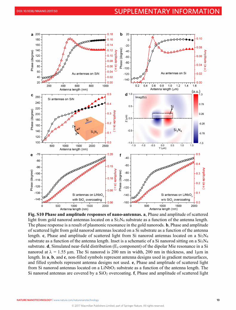
The amplitude and phase response of a nano-antenna is determined using full-wave simulations in the following way. The antenna is placed on an interface between air and an infinitely large substrate of the same material as the waveguide (in case (c) where a SiO2 overcoating is used, the antenna is placed on an interface between SiO2 and an infinitely large substrate of LiNbO3). A plane wave launched from inside the substrate impinges on the interface in the normal direction. The electric-field component of the incident wave is aligned with the nanorod antenna. We monitor the amplitude and phase of the wave scattered from the antenna back into the substrate. The phase responses both in the intermediate-field (i.e., a distance of one wavelength) and in the far-field (i.e., a distance of ~10 wavelengths) are recorded, and are found to be essentially the same. By varying the length of the nanorod antenna, while keeping antenna width and thickness unchanged, we are able to obtain the amplitude and phase responses of the antenna as a function of the antenna length (Fig. S10). The total phase coverage obtained by varying antenna length ranges from 70 degrees to 140 degrees according to the specific materials system used.
To construct a gradient metasurface, we choose a set of antennas with varying lengths so that the phase response changes by a step of d, and arrange the antennas into a linear array with a subwavelength spacing of dx between neighbors, thus creating a constant phase gradient of d/dx along the gradient metasurface.
Fig. S10 Phase and amplitude responses of nano-antennas. a, Phase and amplitude of scattered light from gold nanorod antennas located on a Si3N4 substrate as a function of the antenna length. The phase response is a result of plasmonic resonance in the gold nanorods. b, Phase and amplitude of scattered light from gold nanorod antennas located on a Si substrate as a function of the antenna length. c, Phase and amplitude of scattered light from Si nanorod antennas located on a Si3N4 substrate as a function of the antenna length. Inset is a schematic of a Si nanorod sitting on a Si3N4 substrate. d, Simulated near-field distribution (Ez component) of the dipolar Mie resonance in a Si nanorod at = 1.55 m. The Si nanorod is 200 nm in width, 200 nm in thickness, and 1m in length. In a, b, and c, non-filled symbols represent antenna designs used in gradient metasurfaces, and filled symbols represent antenna designs not used. e, Phase and amplitude of scattered light from Si nanorod antennas located on a LiNbO3 substrate as a function of the antenna length. The Si nanorod antennas are covered by a SiO2 overcoating. f, Phase and amplitude of scattered light
from Si nanorod antennas located on a LiNbO3 substrate as a function of the antenna length. There is no SiO2 overcoating.
The above design procedure monitors the phase response of antennas located on the interface between two semi-infinite media, which is an approximation for antennas patterned on waveguides. To obtain more accurate antenna phase response, we conduct pairs of simulations, one with a bare waveguide and the other with an antenna located on the top surface of the waveguide. By subtracting the field distributions in the two simulations, we are able to obtain the scattered fields of the antenna (some exemplary scattered fields are shown in Fig. S12). In this way, we can determine the phase and amplitude responses of an antenna excited by a waveguide mode. The phase and amplitude responses obtained by this method are essentially the same as those obtained from antennas located on an infinitely large substrate.
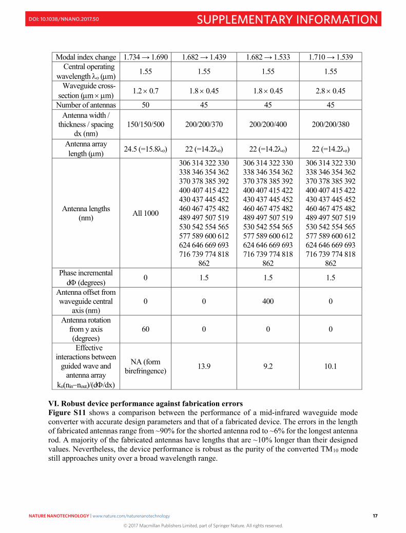
In either the free-space or the waveguide configuration described above, we only monitor the phase and amplitude responses of single isolated antennas, while ignoring the near-field coupling between neighboring antennas in gradient metasurfaces. The near-field coupling could change the phase of the scattered waves from the antennas by a small amount and perturb the phase gradient d/dx so that it is not exactly a constant. Such near-field coupling typically leads to a slight red-shift of the operating wavelength range of our devices, which is not of critical importance because the operating wavelength range of the devices is quite large. V. Device design parameters The device supporting highly asymmetric optical power transmission as shown in Figs. 2 and 3 are based on gold nanorod antennas patterned on Si3N4 waveguides, which are located on a SiO2/Si substrate. The SiO2 layer has a thickness of 4 m to prevent coupling of guided optical power into the Si substrate. The antenna array consists of 56 gold nanorods. Detailed design parameters are provided in Table S2. Table S2 Design parameters of devices supporting asymmetric optical power transmission
Central operating wavelength o (m) 2.45 Dimensions of waveguide cross-section (m m) 2.5 1.0
Number of antennas 56 Antenna width/thickness/spacing (nm) 150/50/300
substrate. The SiO2 layer has a thickness of 5 m. Detailed design parameters are provided in Table S3. Table S3 Design parameters of mid-infrared waveguide mode converters and polarization
The all-dielectric telecom waveguide mode converters and polarization rotator shown in Fig.
6 are based on Si nanorod antennas patterned on LiNbO3 waveguides, which are located on SiO2 substrates. Detailed design parameters are provided in Table S4.
Table S4 Design parameters of telecom wavelength mode converters based on Si/LiNbO3 materials platform
The all-dielectric telecom waveguide mode converters and polarization rotator shown in Fig.
S9 are based on Si nanorod antennas patterned on Si3N4 waveguides, which are located on SiO2/Si substrates. Detailed design parameters are provided in Table S5.
Table S5 Design parameters of telecom waveguide mode converters based on Si/Si3N4 materials platform
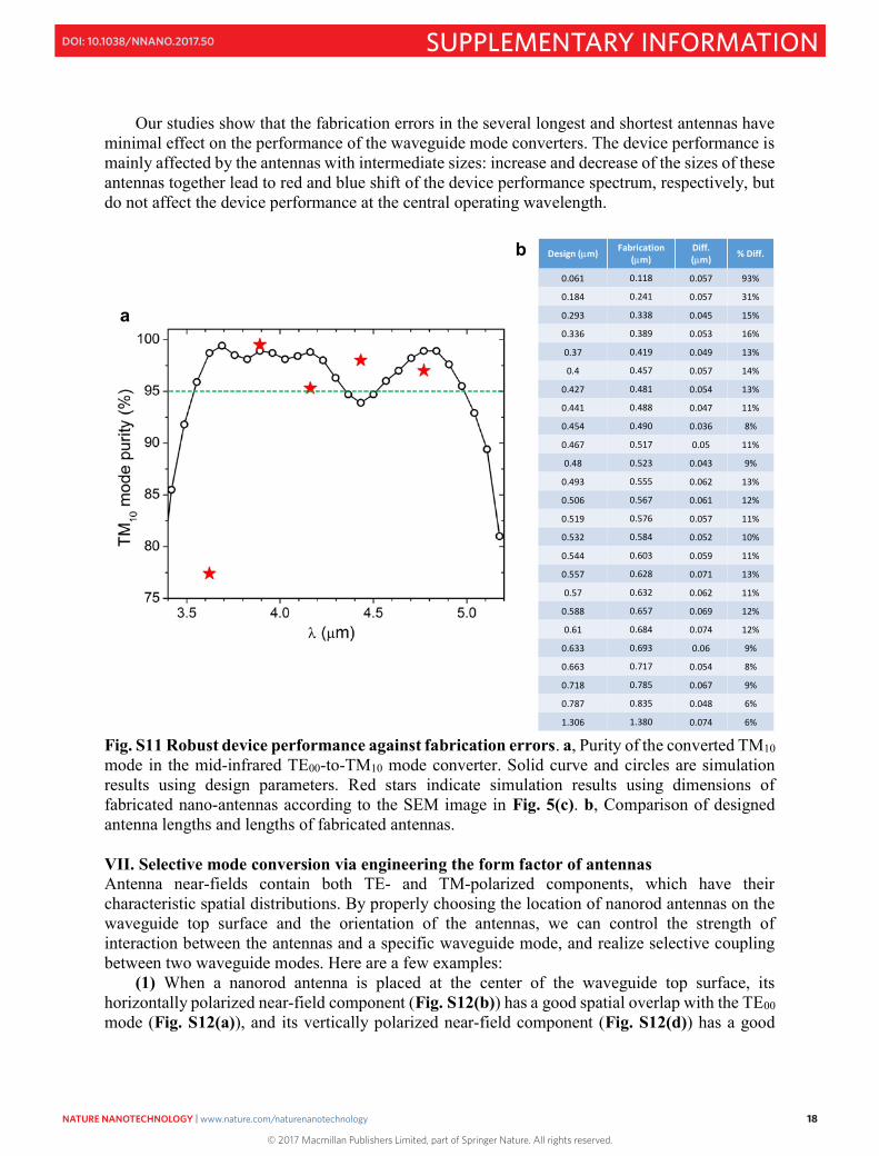
VI. Robust device performance against fabrication errors Figure S11 shows a comparison between the performance of a mid-infrared waveguide mode converter with accurate design parameters and that of a fabricated device. The errors in the length of fabricated antennas range from ~90% for the shorted antenna rod to ~6% for the longest antenna rod. A majority of the fabricated antennas have lengths that are ~10% longer than their designed values. Nevertheless, the device performance is robust as the purity of the converted TM10 mode still approaches unity over a broad wavelength range.
Our studies show that the fabrication errors in the several longest and shortest antennas have minimal effect on the performance of the waveguide mode converters. The device performance is mainly affected by the antennas with intermediate sizes: increase and decrease of the sizes of these antennas together lead to red and blue shift of the device performance spectrum, respectively, but do not affect the device performance at the central operating wavelength.
Fig. S11 Robust device performance against fabrication errors. a, Purity of the converted TM10 mode in the mid-infrared TE00-to-TM10 mode converter. Solid curve and circles are simulation results using design parameters. Red stars indicate simulation results using dimensions of fabricated nano-antennas according to the SEM image in Fig. 5(c). b, Comparison of designed antenna lengths and lengths of fabricated antennas. VII. Selective mode conversion via engineering the form factor of antennas Antenna near-fields contain both TE- and TM-polarized components, which have their characteristic spatial distributions. By properly choosing the location of nanorod antennas on the waveguide top surface and the orientation of the antennas, we can control the strength of interaction between the antennas and a specific waveguide mode, and realize selective coupling between two waveguide modes. Here are a few examples:
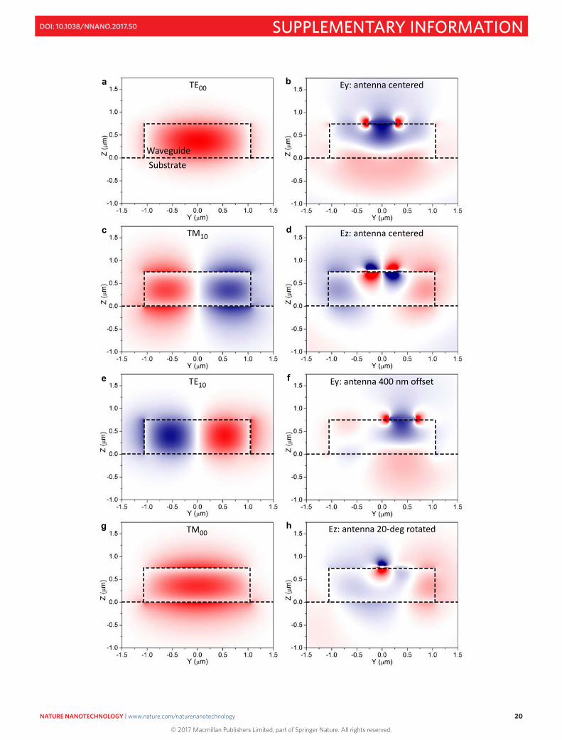
(1) When a nanorod antenna is placed at the center of the waveguide top surface, its horizontally polarized near-field component (Fig. S12(b)) has a good spatial overlap with the TE00 mode (Fig. S12(a)), and its vertically polarized near-field component (Fig. S12(d)) has a good
spatial overlap with the TM10 mode (Fig. S12(c)); therefore, such antenna could have strong interactions with both the TE00 and TM10 modes. The TE00-to-TM10 mode converter in Figs. 4-6, and S9 is based on antennas located at the center of the waveguide top surface.
(2) When a nanorod antenna is displaced from the center of the waveguide (for example, by 400 nm), its horizontally polarized near-field component (Fig. S12(f)) has a non-zero spatial overlap with the TE10 mode (Fig. S12(e)). Therefore, the TE00-to-TE10 mode converter in Figs. 4-6, and S9 is based on such displaced antennas.
(3) When a nanorod antenna is oriented at a non-zero angle (for example, 20 degrees) with respect to the transverse cross-section of the waveguide, its vertically polarized near-field component (Fig. S12(h)) has a non-zero spatial overlap with the TM00 mode (Fig. S12(g)). Therefore, the TE00-to-TM00 mode converter (i.e., polarization rotator) in Figs. 4-6, and S9 is based on such rotated antennas.
Fig. S12 Selective coupling between waveguide modes by engineering the “form factor” of the antenna structure. VIII. Coupled-mode theory for highly asymmetric mode coupling A special coupled-mode theory for describing directional mode coupling (Fig. 2) in our devices can be derived from the conventional coupled-mode theory for two co-propagating waveguide modes:
( ) ( )
( ) ( )
i zab
i zba
a b
da z i b z edz
db z i a z edz
K
(S1)
Here a(z) and b(z) are the amplitude of the two waveguide modes, βa and βb are their propagation constants, ∆β is the wavevector mismatch, z is the propagation direction, and ab and ba are the coupling coefficients between the modes. Specifically,
( , ) ( , ) ( , )
( , ) ( , ) ( , )
ab
ba
A x y a x y b x y dxdy
A x y a x y b x y dxdy
(S2)
where A+ and A are, respectively, the Fourier expansion coefficients of the +K and K wavevector components introduced by the perturbation (z) along the waveguide (Reference: Section 13.4, Amnon Yariv, Optical Electronics in Modern Communications, 5th ed., Oxford University Press, 1997), and the integration is carried in the xy plane (i.e., waveguide transverse cross-section).
Conventionally, a grating patterned on the waveguide is used for mode conversion. The grating provides effective wavevectors ±K of equal magnitude (i.e., A+ = A) so that the +K component compensates the wavevector mismatch when mode a is converted to mode b, and the K component compensates the wavevector mismatch when mode b is converted to mode a. Therefore, under perfect phase matching condition K= βa βb, the above coupled-mode equations become
( ) ( )
( ) ( )
ab
ba
da z i b zdz
db z i a zdz
(S3)
where ab = ba. That is, optical power can be coupled from mode a to mode b and from mode b back to mode a equally easily.
The major difference between our gradient metasurfaces and a conventional grating is that the gradient metasurfaces provide effective wavevectors ±K of different magnitude (i.e., A+ A); that is, the Fourier expansion coefficients of the +K and K wavevector components introduced by the gradient metasurfaces are no longer the same. The metasurface provides a stronger optical scattering when mode a is coupled to mode b, but weaker optical scattering when mode b is coupled back to mode a. Therefore, the coupling coefficients defined in Eq. (S2) are not equal: ab ba. This is our main modification to the conventional coupled-mode theory.
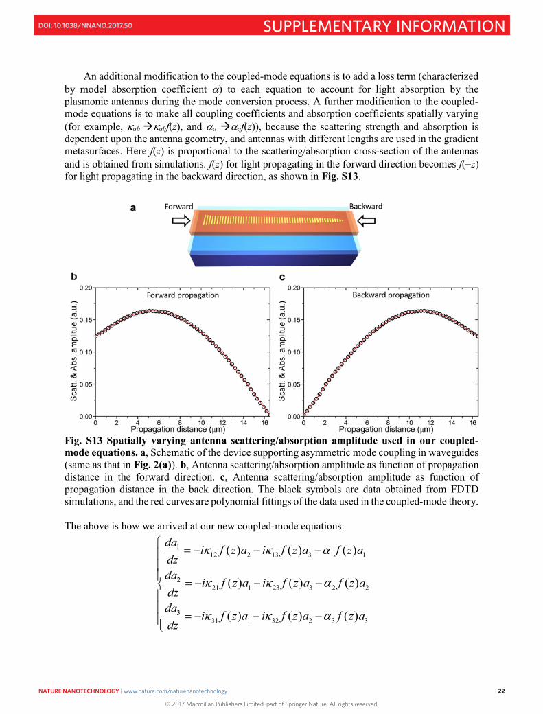
An additional modification to the coupled-mode equations is to add a loss term (characterized by model absorption coefficient ) to each equation to account for light absorption by the plasmonic antennas during the mode conversion process. A further modification to the coupled-mode equations is to make all coupling coefficients and absorption coefficients spatially varying (for example, ab abf(z), and a af(z)), because the scattering strength and absorption is dependent upon the antenna geometry, and antennas with different lengths are used in the gradient metasurfaces. Here f(z) is proportional to the scattering/absorption cross-section of the antennas and is obtained from simulations. f(z) for light propagating in the forward direction becomes f(z) for light propagating in the backward direction, as shown in Fig. S13.
Fig. S13 Spatially varying antenna scattering/absorption amplitude used in our coupled-mode equations. a, Schematic of the device supporting asymmetric mode coupling in waveguides (same as that in Fig. 2(a)). b, Antenna scattering/absorption amplitude as function of propagation distance in the forward direction. c, Antenna scattering/absorption amplitude as function of propagation distance in the back direction. The black symbols are data obtained from FDTD simulations, and the red curves are polynomial fittings of the data used in the coupled-mode theory. The above is how we arrived at our new coupled-mode equations:
112 2 13 3 1 1
221 1 23 3 2 2
331 1 32 2 3 3
( ) ( ) ( )
( ) ( ) ( )
( ) ( ) ( )
da i f z a i f z a f z adzda i f z a i f z a f z adzda i f z a i f z a f z adz
where a1, a2 and a3 represent the amplitudes of the TE00 mode, the TM10 mode, and the surface wave, respectively; ab is the coupling coefficient that governs the efficiency of coupling from mode b to mode a, and ab ba; a is the absorption coefficient of mode a.
The derivation of this new coupled mode theory is completely based on conventional coupled mode theory and on physical properties of our gradient metasurfaces (i.e., asymmetric Fourier expansion coefficients of the waveguide perturbation: A+ A, loss due to absorption in plasmonic metasurfaces, and spatial variation of the scattering and absorption coefficients).
The parameters used to fit simulated mode evolutions in Figs. 2(f) and 2(g) are listed in Table S6.
Table S6 Fitting parameters used in the coupled mode equations for Figs. 2(f)-(g)
12 (m-1)
21 13 31 23 32 1 2 3
Backward 0 0 1.1 5.9 0 0 0.26 0 0.8
Forward 0 0 1.2 0.8 1.2 0.3 0.12 0.1 0.1
In Table S6, the coupling coefficients 12 and 21 are set to be zero for both the forward and
backward propagation directions. This due to the fact that the TE00 and TM10 modes have small overlap with each other even in the presence of the metasurfaces compared with the overlap between either mode with the surface wave (e.g., 12 <<13).
In the backward propagation direction, the asymmetric wavevector/phase gradient provided by the gradient metasurface leads to a continuous increase of the wavevector. As a result, the incident TE00 mode couples efficiently into a surface wave supported by the antenna array (i.e., 31 is large). The asymmetry of the phase gradient ensures that optical power won’t be coupled back from the surface wave to the TE00 mode efficiently (i.e., 13 is small). Therefore, Table S6 shows that 31 is much larger than 13. The absorption coefficient 3 for the surface wave is much larger than that of the TE00 mode, 1, because of the much stronger interaction between the surface wave and the antenna array. In our full-wave simulations in which the TE00 mode is launched into the device in the backward direction, we observed that the input TE00 mode is directly converted into surface waves, and that there is no TM10 mode generated at any location of the device. This observation motivated us to neglect the TM10 mode in the backward propagation direction by taking 23 and 32, as well as 2 to be zero in Table S6.
In the forward propagation direction (i.e., mode conversion), the gradient metasurface causes a decrease of the wavevector. Therefore, it is favorable for optical power to couple from the surface wave to the TE00 (TM10) mode and the opposite process is less efficient. This is the reason that in Table S6, 13 (23) that governs the coupling from the surface wave to the TE00 (TM10) mode is larger than 31 (32) that governs the coupling from the TE00 (TM10 mode) to the surface wave.
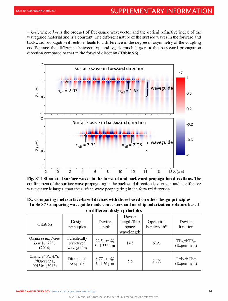
The nature of the surface waves in the forward and backward propagation directions are different. Our FDTD simulations show that the surface wave in the backward propagation direction is much more confined to the antenna array and has a much larger effective wavevector compared to the surface wave in the forward propagation direction (Fig. S14). This is because in the backward propagation direction the gradient metasurface causes a continuous increase of the longitudinal component k|| of the wavevector of the surface wave, and therefore a continuous increase of the transverse component ik of the wavevector, which is imaginary and characterizes the confinement of the surface wave. k|| and ik are related by the dispersion relation: (k||)2 + (ik)2
= keff2, where keff is the product of free-space wavevector and the optical refractive index of the
waveguide material and is a constant. The different nature of the surface waves in the forward and backward propagation directions leads to a difference in the degree of asymmetry of the coupling coefficients: the difference between 31 and 13 is much larger in the backward propagation direction compared to that in the forward direction (Table S6).
Fig. S14 Simulated surface waves in the forward and backward propagation directions. The confinement of the surface wave propagating in the backward direction is stronger, and its effective wavevector is larger, than the surface wave propagating in the forward direction. IX. Comparing metasurface-based devices with those based on other design principles Table S7 Comparing waveguide mode converters and on-chip polarization rotators based
lattice constant of 0.4 times of free-space wavelength
2 1.8% TE00TE10 (Theory, 2D
design)
Alonso-Ramos et al.,
Opt. Lett. 37, 335 (2012)
Tapered waveguide+
Double-etched directional
coupler
~800 m @ =1.55 m >516 >2.2% TE00TM00
(Theory)
Dai et al., Opt. Express
19, 10940 (2011)
Adiabatic taper + asymmetrical
directional coupler
~100 m @ =1.55 m 64.5 3.9% TM00TE00
(Theory)
Our work Phase-
gradient metasurfaces
5.420.3 m @ =1.55 m (Table
S4), 7.512 m @ =4 m (Table S3)
3.513.1 @ =1.55 m (Table S4), 1.72.9 @ =4 m
(Table S3)
>6.5% (Experiment) 35% (Theory)
TE00TM00, TE00TE10, &
TE00TM10 (Experiment) TE00TE20
(Theory)
*Operation bandwidth is defined as the wavelength range over which the conversion efficiency is larger than 90% (or conversion loss smaller than ~0.46 dB) divided by the central operating wavelength.
Tables S7 summarizes the design principles and performance of waveguide mode converters and on-chip polarization rotators reported in the literature and of our devices based on phase-gradient metasurfaces. The summary focuses primarily on experimental work. The smallest devices we have experimentally demonstrated (i.e., TE00-to-TE10 mode converter and TE00-to-TM00 polarization rotator in the mid-infrared) have lengths that are just 1.7-1.8 times of the free-space wavelength (Table S3), which, to the best of our knowledge, are the most compact devices demonstrated so far (including both theoretical and experimental demonstrations). The device operation bandwidths we have demonstrated (i.e., >6.5% in experiments and 35% in theory) are the largest among all devices demonstrated so far. The record small device footprint and large operation bandwidth are owing to the strong scattering of waveguide modes at subwavelength intervals provided by the metasurface structures, which is the most unique aspect of our design.