Print: ISBN 0-7381-2944-5 SH94949PDF: ISBN 0-7381-2945-3 SS94949
No part of this publication may be reproduced in any form, in an electronic retrieval system or otherwise, without the prior written permission of the publisher.
IEEE Std 1149.1-2001(Revision of IEEE Std 1149.1-1990)
IEEE Standard Test Access Port and Boundary-Scan Architecture
Sponsor
Test Technology Standards Committeeof theIEEE Computer Society
Approved 14 June 2001
IEEE-SA Standards Board
Abstract: Circuitry that may be built into an integrated circuit to assist in the test, maintenance, andsupport of assembled printed circuit boards is defined. The circuitry includes a standard interfacethrough which instructions and test data are communicated. A set of test features is defined,including a boundary-scan register, such that the component is able to respond to a minimum setof instructions designed to assist with testing of assembled printed circuit boards. Also, a languageis defined that allows rigorous description of the component-specific aspects of such testabilityfeatures.Keywords: boundary scan, boundary-scan architecture, Boundary-Scan Description Language,boundary-scan register, BSDL, circuit boards, circuitry, integrated circuit, printed circuit boards,TAP, test, test access port, VHDL, VHSIC Hardware Description Language
IEEE Standards documents are developed within the IEEE Societies and the Standards Coordinating Committees of theIEEE Standards Association (IEEE-SA) Standards Board. The IEEE develops its standards through a consensus develop-ment process, approved by the American National Standards Institute, which brings together volunteers representing variedviewpoints and interests to achieve the final product. Volunteers are not necessarily members of the Institute and serve with-out compensation. While the IEEE administers the process and establishes rules to promote fairness in the consensus devel-opment process, the IEEE does not independently evaluate, test, or verify the accuracy of any of the information containedin its standards.
Use of an IEEE Standard is wholly voluntary. The IEEE disclaims liability for any personal injury, property or other dam-age, of any nature whatsoever, whether special, indirect, consequential, or compensatory, directly or indirectly resultingfrom the publication, use of, or reliance upon this, or any other IEEE Standard document.
The IEEE does not warrant or represent the accuracy or content of the material contained herein, and expressly disclaimsany express or implied warranty, including any implied warranty of merchantability or fitness for a specific purpose, or thatthe use of the material contained herein is free from patent infringement. IEEE Standards documents are supplied “AS IS.”
The existence of an IEEE Standard does not imply that there are no other ways to produce, test, measure, purchase, market,or provide other goods and services related to the scope of the IEEE Standard. Furthermore, the viewpoint expressed at thetime a standard is approved and issued is subject to change brought about through developments in the state of the art andcomments received from users of the standard. Every IEEE Standard is subjected to review at least every five years for revi-sion or reaffirmation. When a document is more than five years old and has not been reaffirmed, it is reasonable to concludethat its contents, although still of some value, do not wholly reflect the present state of the art. Users are cautioned to checkto determine that they have the latest edition of any IEEE Standard.
In publishing and making this document available, the IEEE is not suggesting or rendering professional or other servicesfor, or on behalf of, any person or entity. Nor is the IEEE undertaking to perform any duty owed by any other person orentity to another. Any person utilizing this, and any other IEEE Standards document, should rely upon the advice of a com-petent professional in determining the exercise of reasonable care in any given circumstances.
Interpretations: Occasionally questions may arise regarding the meaning of portions of standards as they relate to specificapplications. When the need for interpretations is brought to the attention of IEEE, the Institute will initiate action to prepareappropriate responses. Since IEEE Standards represent a consensus of concerned interests, it is important to ensure that anyinterpretation has also received the concurrence of a balance of interests. For this reason, IEEE and the members of its soci-eties and Standards Coordinating Committees are not able to provide an instant response to interpretation requests except inthose cases where the matter has previously received formal consideration.
Comments for revision of IEEE Standards are welcome from any interested party, regardless of membership affiliation withIEEE. Suggestions for changes in documents should be in the form of a proposed change of text, together with appropriatesupporting comments. Comments on standards and requests for interpretations should be addressed to:
IEEE is the sole entity that may authorize the use of certification marks, trademarks, or other designations to indicate com-pliance with the materials set forth herein.
Authorization to photocopy portions of any individual standard for internal or personal use is granted by the Institute ofElectrical and Electronics Engineers, Inc., provided that the appropriate fee is paid to Copyright Clearance Center. Toarrange for payment of licensing fee, please contact Copyright Clearance Center, Customer Service, 222 Rosewood Drive,Danvers, MA 01923 USA; (978) 750-8400. Permission to photocopy portions of any individual standard for educationalclassroom use can also be obtained through the Copyright Clearance Center.
Note: Attention is called to the possibility that implementation of this standard may require use of subject mat-ter covered by patent rights. By publication of this standard, no position is taken with respect to the existence orvalidity of any patent rights in connection therewith. The IEEE shall not be responsible for identifying patentsfor which a license may be required by an IEEE standard or for conducting inquiries into the legal validity orscope of those patents that are brought to its attention.
(This introduction is not part of IEEE Std 1149.1-2001, Standard Test Access Port and Boundary-Scan Architecture.)
This standard defines a test access port and boundary-scan architecture for digital integrated circuits and forthe digital portions of mixed analog/digital integrated circuits. The facilities defined by the standard seek toprovide a solution to the problem of testing assembled printed circuit boards and other products based onhighly complex digital integrated circuits and high-density surface-mounting assembly techniques. Theyalso provide a means of accessing and controlling design-for-test features built into the digital integrated cir-cuits themselves. Such features might, for example, include internal scan paths and self-test functions aswell as other features intended to support service applications in the assembled product.
History of the development of this standard
The process of developing this standard began in 1985, when the Joint European Test Action Group(JETAG) was formed in Europe. During 1986, this group expanded to include members from both Europeand North America and, as a result, was renamed the Joint Test Action Group (JTAG). Between 1986 and1988, the JTAG Technical Subcommittee developed and published a series of proposals for a standardizedform of boundary scan. In 1988, the last of these proposals—JTAG Version 2.0—was offered to the IEEETestability Bus Standards Committee (P1149) for inclusion in the standard then under development. TheTestability Bus Standards Committee accepted this approach. It decided that the JTAG proposal shouldbecome the basis of a standard within the Testability Bus family, with the result that the P1149.1 project wasinitiated. Following these decisions, the JTAG Technical Subcommittee became the core of the IEEE Work-ing Group that developed this standard.
After the initial approval of this standard in February 1990 and its subsequent publication, the WorkingGroup immediately began efforts to develop a supplement for the purpose of correction, clarification, andenhancement. This effort, spurred and guided by interaction between developers and users of the originalstandard, culminated in IEEE Std 1149.1a-1993, which was approved in June 1993.
The major changes to this standard introduced by IEEE Std 1149.1a-1993 were
— The addition of two optional instructions, CLAMP and HIGHZ, which standardized the names andspecifications of features often implemented as design-specific features
— The addition of an optional facility to switch a component from a mode in which it complies to thisstandard into one in which it supports another design-for-test approach
Further, starting with a proposal made by Kenneth P. Parker and Stig Oresjo in 1990, an effort was under-taken to develop a language to describe components that conform to this standard. This effort concluded inthe approval of IEEE Std 1149.1b-1994 in September 1994.
The major change introduced to this standard by IEEE Std 1149.1b-1994 was the addition of Annex B,which defines the Boundary-Scan Description Language. All other changes were minor and were strictly forclarification.
Changes introduced by this revision
This revision is primarily a housekeeping update, designed to consolidate learning from the first 10 years ofthe standard’s use into the standard document.
— To reduce the risk of accidental entry into test mode, the requirement that a binary code for theEXTEST instruction be {000...0} has been removed and use of this binary code for other instruc-tions that result in entry to test mode has been deprecated [see 8.1.1 e), 8.8.1 h), B.8.11.3 d), andB.8.11.3 e )].
— To increase the flexibility with which instructions may be implemented and merged, the implicitlymerged SAMPLE/PRELOAD instruction has been redefined as two separate instructions: SAMPLEand PRELOAD. These instructions can continue to share a single binary code, effectively resultingin a merged SAMPLE/PRELOAD instruction, but alternatively, they may now share binary codeswith other instructions, provided that no rules for any of the merged instructions are violated. [see8.1.1 g), 8.2.1 b), 8.6, 8.7, B.5.1.2, B.6.3 b), B.8.11.3 f), B.8.11.3 g), B.8.11.3 h), B.8.11.3 i),B.8.11.3 j), and B.8.13.3 a)].
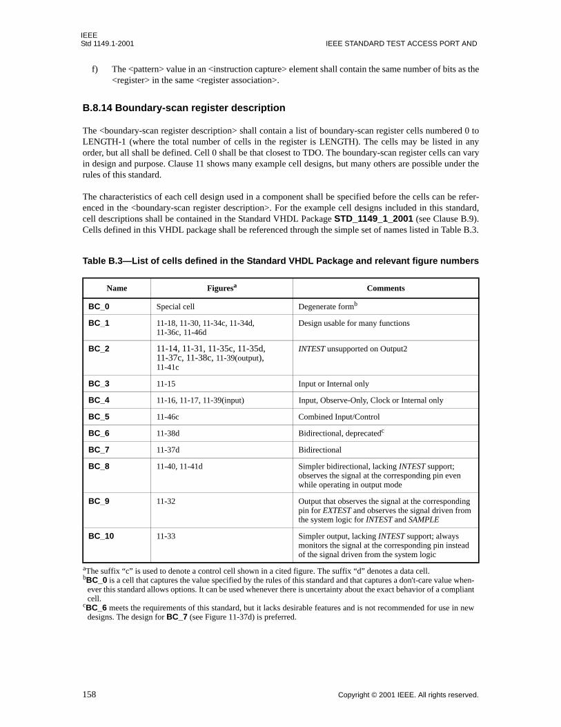
— To enable more efficient implementation of boundary-scan register cells provided at system logicoutputs, the source of data to be captured in such cells in response to the SAMPLE instruction isnow allowed to be at the connected system pin [see 8.6.1 d), 11.6.1 a), 11.6.1 b), B.8.14.4 l), andB.10.2.4.1 b)]. Additionally, three new cell types based on this implementation (BC_8, BC_9, andBC_10) have been added to the Standard VHDL Package (see B.5.1.2, B.9, and Table B.3).
— To permit more flexible boundary-scan register cell implementations, sharing of circuitry betweenthe boundary-scan register and other elements of the test and/or system logic has been allowed inlimited cases [see 11.2.1 j) and 11.2.1 k)].
— To support more complete description of IC pin drivers with bus keeper circuits, a new value for<disable result> has been defined (KEEPER, see B.5.1.2, B.8.14.1, and B.8.14.3.7).
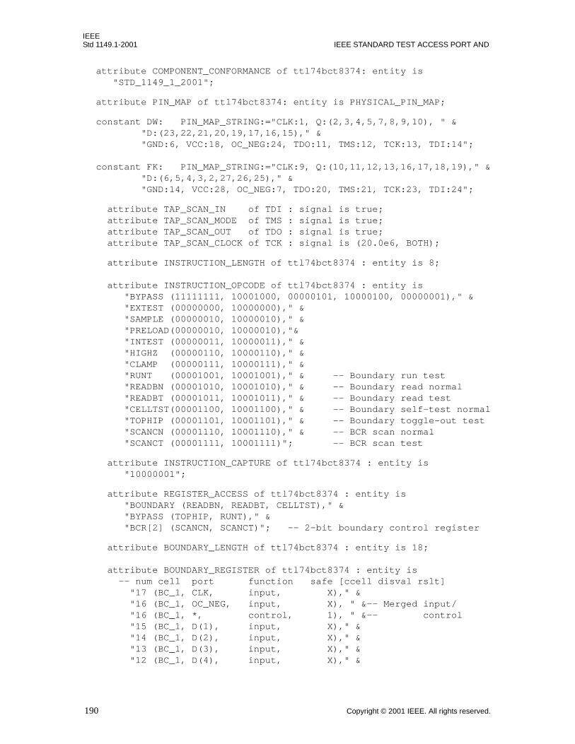
— To track the widespread acceptance of BSDL, the language has been made a normative part of thestandard and its use for documentation has been mandated (see 13.3.1 c) and Annex B).
Additionally, a number of minor changes were made to correct and clarify the language of the standard [ofspecial note, see 4.8.1 c), 11.7.1 b), B.8.14.4 k), and B.8.14.4 n)].
Participants
At the time of the issue of IEEE Std 1149.1-2001, the members of the working group were:
Christopher J. Clark, Chair
Adam W. Ley, Editor
John AndrewsBill AronsonCarl F. BarnhartDilip K. BhavsarTerry BorrozJohn BradenBill BruceTapan J. ChakrabortySung ChungJim ColemanFrans De JongBulent Dervisoglu
Ted EatonBill EklowDean GeerdesGrady L. GilesPeter HansenNeil JacobsonNajmi JarwalaLondon JinWuudiann KeArthur KhuRamesh KrishnamurthyTom LangfordLarry Lee
Colin MaunderBenoit Nadeau-DostieJay NejedloKenneth P. ParkerMichael RicchettiGordon D. RobinsonRobert J. RussellAdam SheppardSteve StarkRon WaltherLee WhetselThomas W. Williams
The following members of the balloting group voted on this standard. Balloters may have voted forapproval, disapproval, or abstention. :
When the IEEE-SA Standards Board approved this standard on 14 June 2001, it had the followingmembership:
Donald N. Heirman, ChairJames T. Carlo, Vice ChairJudith Gorman, Secretary
*Member Emeritus
Also included are the following nonvoting IEEE-SA Standards Board liaison:
Alan Cookson, NIST RepresentativeDonald R. Volzka, TAB Representative
Don MessinaIEEE Standards Project Editor
John AndrewsCarl BarnhartRoger BennettsTerry BorrozJohn BradenKeith ChowSung S. ChungChris J. ClarkFrans de JongTed EatonWilliam EklowDean Geerdes
Grady GilesPeter HansenLee F. HorneyMitsuaki IshikawaNeil JacobsonJake KarrfaltThomas L. LangfordAdam W. LeyGregory A. MastonColin MaunderPatrick McHugh
Earl J. MeiersYinghua MinJames A. MonzelBenoit Nadeau-DostieJay NejedloBruce E. PetersonMike RicchettiGordon RobinsonJaideep RoyRobert J. RussellScott A. YalcourtT. W. Williams
Satish K. AggarwalMark D. BowmanGary R. EngmannHarold E. EpsteinH. Landis FloydJay Forster*Howard M. FrazierRuben D. Garzon
James H. GurneyRichard J. HollemanLowell G. JohnsonRobert J. KennellyJoseph L. Koepfinger*Peter H. LipsL. Bruce McClungDaleep C. Mohla
James W. MooreRobert F. MunznerRonald C. PetersenGerald H. PetersonJohn B. PoseyGary S. RobinsonAkio TojoDonald W. Zipse
4. Test access port (TAP)......................................................................................................................... 9
4.1 Connections that form the test access port (TAP) ...................................................................... 94.2 Test clock input (TCK) ................................................................................................................ 94.3 Test mode select input (TMS) ................................................................................................... 114.4 Test data input (TDI) ................................................................................................................. 114.5 Test data output (TDO).............................................................................................................. 124.6 Test reset input (TRST*) ........................................................................................................... 124.7 Interconnection of components compatible with this standard ................................................. 134.8 Subordination of this standard within a higher-level test strategy............................................. 15
5. Test logic architecture........................................................................................................................ 16
5.1 Test logic design ........................................................................................................................ 175.2 Test logic realization.................................................................................................................. 17
6. The TAP controller ............................................................................................................................ 18
6.1 TAP controller state diagram..................................................................................................... 186.2 TAP controller operation .......................................................................................................... 246.3 TAP controller initialization ...................................................................................................... 30
7. The instruction register ...................................................................................................................... 33
7.1 Design and construction of the instruction register ................................................................... 337.2 Instruction register operation ..................................................................................................... 34
8.1 Response of the test logic to instructions................................................................................... 368.2 Public instructions...................................................................................................................... 378.3 Private instructions .................................................................................................................... 388.4 The BYPASS instruction............................................................................................................. 388.5 Boundary-scan register instructions........................................................................................... 398.6 The SAMPLE instruction ........................................................................................................... 418.7 The PRELOAD instruction ........................................................................................................ 438.8 The EXTEST instruction ............................................................................................................ 45
8.9 The INTEST instruction ............................................................................................................. 488.10 The RUNBIST instruction .......................................................................................................... 538.11 The CLAMP instruction ............................................................................................................. 568.12 Device identification register instructions ................................................................................. 578.13 The IDCODE instruction ........................................................................................................... 588.14 The USERCODE instruction ..................................................................................................... 588.15 The HIGHZ instruction.............................................................................................................. 59
9. Test data registers .............................................................................................................................. 61
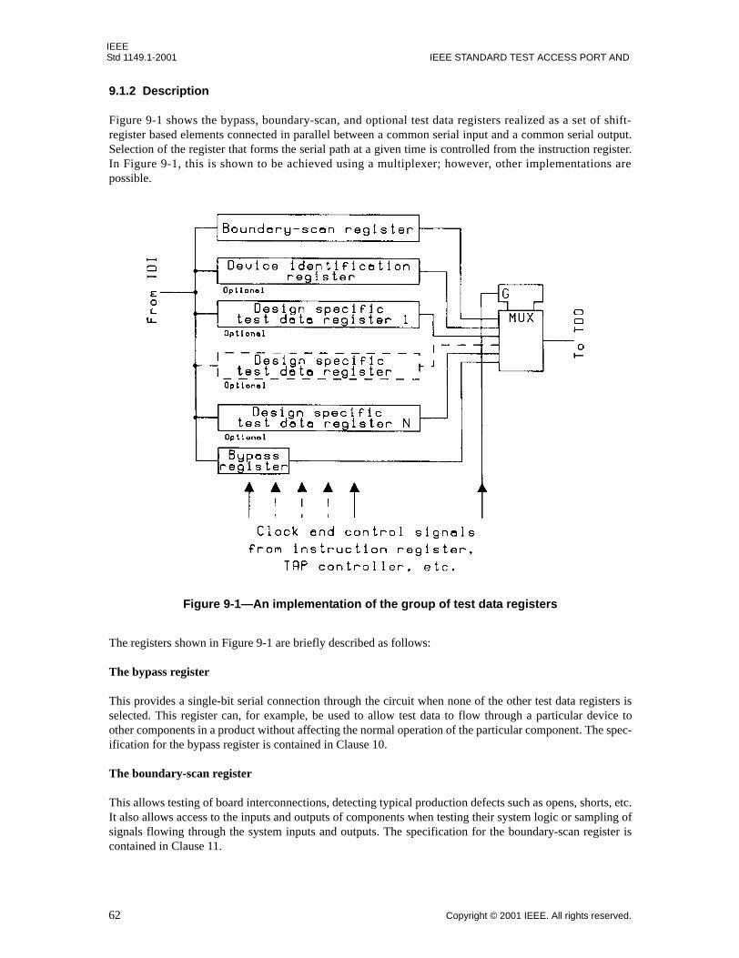
9.1 Provision of test data registers ................................................................................................... 619.2 Design and construction of test data registers ........................................................................... 639.3 Test data register operation........................................................................................................ 64
10. The bypass register ............................................................................................................................ 66
10.1 Design and operation of the bypass register .............................................................................. 66
11. The boundary-scan register................................................................................................................ 67
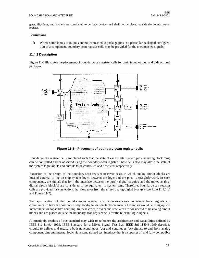
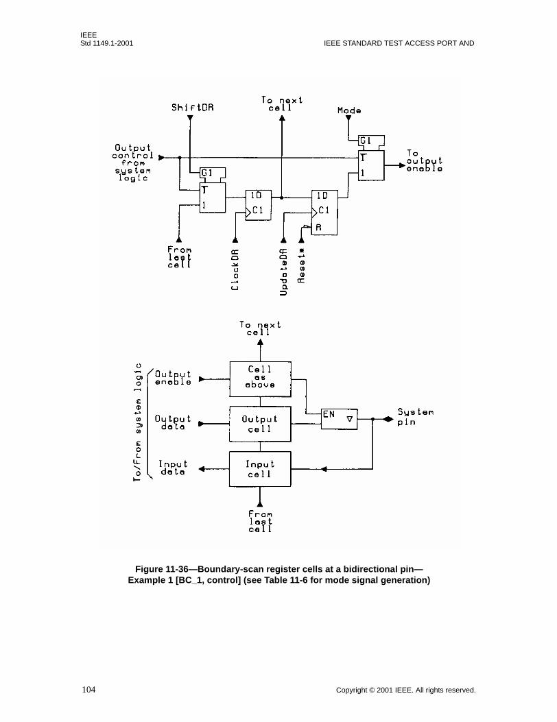
11.1 Introduction................................................................................................................................ 6811.2 Register design........................................................................................................................... 7211.3 Register operation ...................................................................................................................... 7411.4 General rules regarding cell provision....................................................................................... 7611.5 Provision and operation of cells at system logic inputs............................................................. 7911.6 Provision and operation of cells at system logic outputs........................................................... 8711.7 Provision and operation of cells at bidirectional system logic pins......................................... 10211.8 Redundant cells........................................................................................................................ 10811.9 Special cases ............................................................................................................................ 109
12. The device identification register .................................................................................................... 111
12.1 Design and operation of the device identification register ...................................................... 11212.2 Manufacturer identity code...................................................................................................... 11412.3 Part-number code ..................................................................................................................... 11512.4 Version code ............................................................................................................................ 115
13. Conformance and documentation requirements .............................................................................. 115
13.1 Claiming conformance to this standard ................................................................................... 11513.2 Prime and second source components ..................................................................................... 11713.3 Documentation requirements ................................................................................................... 117
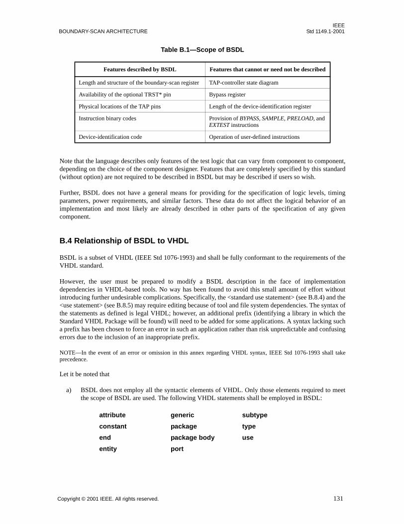
Annex A (informative) An example implementation using level-sensitive design techniques................... 120Annex B (normative) Boundary-scan description language........................................................................ 129
IEEE Standard Test Access Port and Boundary-Scan Architecture
1. Overview
1.1 Scope
This standard defines test logic that can be included in an integrated circuit to provide standardizedapproaches to
— testing the interconnections between integrated circuits once they have been assembled onto aprinted circuit board or other substrate;
— testing the integrated circuit itself; and— observing or modifying circuit activity during the component's normal operation.
The test logic consists of a boundary-scan register and other building blocks and is accessed through a TestAccess Port (TAP).
1.2 Purpose
1.2.1 An overview of the operation of IEEE Std 1149.1
This subclause provides a general overview of the operation of a component compatible with this standardand provides a background to the detailed discussion in later subclauses.
The circuitry defined by this standard allows test instructions and associated test data to be fed into acomponent and, subsequently, allows the results of execution of such instructions to be read out. Allinformation (instructions, test data, and test results) is communicated in a serial format.
The sequence of operations would be controlled by a bus master, which could be either an automatic testequipment (ATE) or a component that interfaces to a higher-level test bus as a part of a complete systemmaintenance architecture. Control is achieved through signals applied to the Test Mode Select (TMS) andTest Clock (TCK) inputs of the various components connected to the bus master. Starting from an initialstate in which the test circuitry defined by this standard is inactive, a typical sequence of operations wouldbe as follows.
IEEEStd 1149.1-2001 IEEE STANDARD TEST ACCESS PORT AND
The first steps would be, in general, to load serially into the component the instruction binary code for theparticular operation to be performed. The test logic defined by this standard is designed such that the serialmovement of instruction information is not apparent to those circuit blocks whose operation is controlled bythe instruction. The instruction applied to these blocks changes only on completion of the shifting (instruc-tion load) process.
Once the instruction has been loaded, the selected test circuitry is configured to respond. In some cases,however, it is necessary to load data into the selected test circuitry before a meaningful response can bemade. Such data is loaded into the component serially in a manner analogous to the process used previouslyto load the instruction. Note that the movement of test data has no effect on the instruction present in the testcircuitry.
After execution of the test instruction, based where necessary on supplied data, the results of the test can beexamined by shifting data out of the component to or through the bus master.
Note that in cases where the same test operation is to be repeated but with different data, new test data can beshifted into the component while the test results are shifted out. There is no need for the instruction to bereloaded.
Operation of the test circuitry may proceed by loading and executing several further instructions in a mannersimilar to that described and would conclude by returning the test circuitry and, where required, on-chipsystem circuitry to its initial state.
1.2.2 The use of IEEE Std 1149.1 to test an assembled product
This subclause outlines the use of the boundary-scan circuitry defined by this standard during the process oftesting an assembled product such as a printed circuit board.
The test problem for any product constructed from a collection of components can be decomposed into threegoals:
a) To confirm that each component performs its required function;b) To confirm that the components are interconnected in the correct manner; andc) To confirm that the components in the product interact correctly and that the product performs its
intended function.
This approach can be applied to a board constructed from integrated circuits, to a system constructed fromprinted circuit boards, or to a complex integrated circuit constructed from a set of simpler functionalmodules. To simplify the discussion, this description henceforth will concentrate on the case of anassembled printed circuit board constructed from a collection of digital integrated circuits.
At the board level, goal a) and goal b) typically are achieved by using in-circuit test techniques; for goal c),a functional test is required. However, in-circuit test techniques have significant limitations when viewedagainst evolving surface-mount interconnection technology, for example, the difficulty of making reliablecontact to miniaturized features of the printed circuit board using a bed-of-nails fixture. How, then, might theabove three test goals be achieved if test access becomes limited to the normal circuit connections, plus arelatively small number of special-purpose test connections?
Considering goal a), it is clear that the vendor of an integrated circuit used in the board-level design will havean established test methodology for that component. The components could be tested on a proprietary ATEsystem or by using a self-test procedure embedded in the design. Information on the test methodologyadopted is typically not available to the component purchaser. Even where self-test modes of operation areknown to exist, they may not be documented and therefore are not available to the component user.Alternative sources of test data for the board test engineer may be the component test libraries supplied with
in-circuit test systems or the test programs developed by component users for incoming inspection ofdelivered devices.
Wherever the test data for a component originates, the next step is to use it once the component has beenassembled onto the printed circuit board. If access is limited to the normal connections of the assembledcircuit, this task may be far from simple. This is particularly true if the surrounding components are complexor if the board designer has tied some of the components’ connections to fixed logic levels or has leftcomponent pins unconnected. Normally, it will not be possible to test the component in the same way that itwas tested in isolation unless an in-circuit test is achievable.
To ensure that built-in test facilities can be used or that preexisting test patterns can be applied, a frameworkis needed that can be used to convey test data to or from the boundaries of individual components so thatthey can be tested as if they were freestanding. This framework will also allow access to and control of built-in test facilities of components. Boundary scan coupled with a test access bus provides such a framework.
The objective of this standard is to define a boundary-scan architecture that can be adopted as a standardfeature of integrated circuit designs, thus allowing the required test framework to be created on assembledprinted circuit boards and other products.
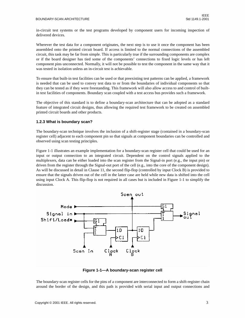
1.2.3 What is boundary scan?
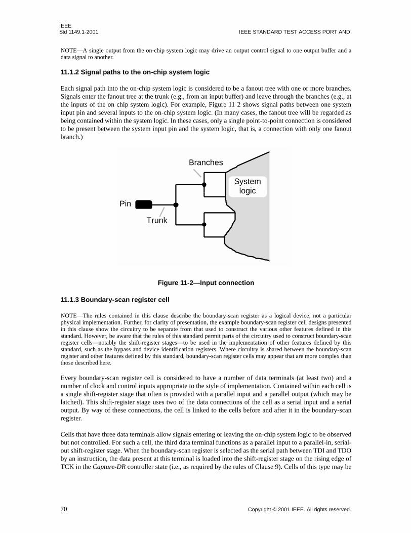
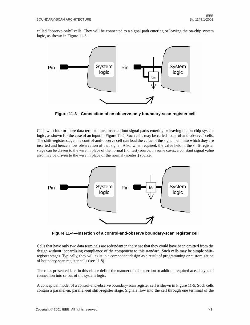
The boundary-scan technique involves the inclusion of a shift-register stage (contained in a boundary-scanregister cell) adjacent to each component pin so that signals at component boundaries can be controlled andobserved using scan testing principles.
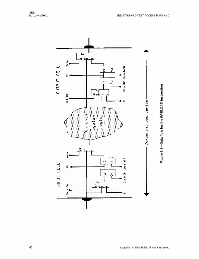
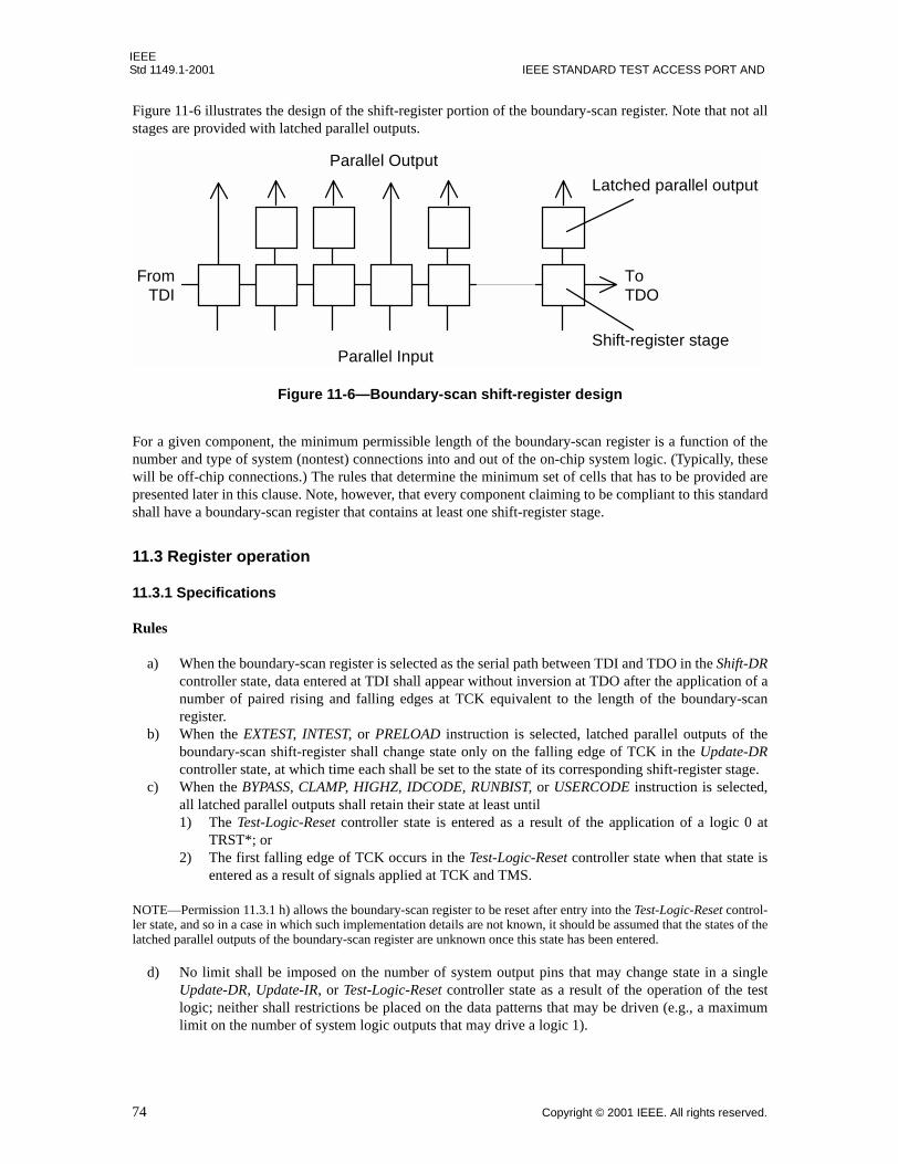
Figure 1-1 illustrates an example implementation for a boundary-scan register cell that could be used for aninput or output connection to an integrated circuit. Dependent on the control signals applied to themultiplexers, data can be either loaded into the scan register from the Signal-in port (e.g., the input pin) ordriven from the register through the Signal-out port of the cell (e.g., into the core of the component design).As will be discussed in detail in Clause 11, the second flip-flop (controlled by input Clock B) is provided toensure that the signals driven out of the cell in the latter case are held while new data is shifted into the cellusing input Clock A. This flip-flop is not required in all cases but is included in Figure 1-1 to simplify thediscussion.
The boundary-scan register cells for the pins of a component are interconnected to form a shift-register chainaround the border of the design, and this path is provided with serial input and output connections and
Figure 1-1—A boundary-scan register cell
IEEEStd 1149.1-2001 IEEE STANDARD TEST ACCESS PORT AND
appropriate clock and control signals. Within a product assembled from several integrated circuits theboundary-scan registers for the individual components could be connected in series to form a single paththrough the complete design, as illustrated in Figure 1-2. Alternatively, a board design could contain severalindependent boundary-scan paths.
If all the components used to construct a circuit have a boundary-scan register, the resulting serial paththrough the complete design can be used in two ways:
a) To allow the interconnections between the various components to be tested, test data can be shiftedinto all the boundary-scan register cells associated with component output pins and loaded in paral-lel through the component interconnections into those cells associated with input pins; and
b) To allow the components on the board to be tested, the boundary-scan register can be used as ameans of isolating on-chip system logic from stimuli received from surrounding components whilean internal self-test is performed. Alternatively, if the boundary-scan register is suitably designed, itcan permit a limited slow-speed static test of the on-chip system logic since it allows delivery of testdata to the component and examination of the test results.
These tests allow the first two goals discussed earlier to be achieved through the use of the boundary-scanregister. In effect, tests applied using the register can detect many of the faults that in-circuit testers currentlyaddress, but without the need for extensive bed-of-nails access. The third goal—to functionally test theoperation of the complete product—remains and can be achieved either by using a functional (through thepins) ATE system or by using a system-level self-test, for example.
Note also that by parallel loading the cells at both the inputs and outputs of a component and shifting out theresults, the boundary-scan register provides a means of “sampling” the data flowing through a componentwithout interfering with the behavior of the component or the assembled board. This mode of operation isvaluable for design debugging and fault diagnosis since it permits examination of connections not normallyaccessible to the test system.
1.2.4 The use of IEEE Std 1149.1 to achieve other test goals
In addition to its application in testing printed circuit assemblies and other products containing multiplecomponents, the test logic defined by this standard can be used to provide access to a wide range of design-
for-test features built into the components themselves. Such features might include internal scan paths, self-test functions [e.g., using built-in logic block observer (BILBO) elements], or other support functions.
Design-for-test features such as these can be accessed and controlled using the data path between the serialtest data pins of the TAP defined by this standard. Instructions that cause internal reconfiguration of thecomponent's system logic such that the test operation is enabled may be shifted into the component throughthe TAP.
1.3 Document outline
Circuit designs such as that defined by this standard are more easily understood if their specifications areaccompanied by general descriptive material that places the details of the various parts of the design inperspective and provides examples of implementation. Clause 1 therefore contains an overview of theapplication of this standard to the testing of the digital portions of an electronic product consisting of manyintegrated circuits.
Subsequent clauses of the document contain the specifications for particular features of this standard. Twoclasses of material are contained in these clauses:
1.3.1 Specifications
Subclauses entitled Specifications contain the rules, recommendations, and permissions that define thisstandard:
a) Rules specify the mandatory aspects of this standard. Subclauses that are rules contain the wordshall.
b) Recommendations indicate preferred practice for designs that seek to conform to this standard. Sub-clauses that are recommendations contain the word should.
c) Permissions show how optional features may be introduced into a design that seeks to conform tothis standard. These features will extend the application of the test circuitry defined by this standard.Subclauses that are permissions contain the word may.
1.3.2 Descriptions
Material not contained in subclauses entitled Specifications is descriptive material that illustrates the needfor the features being specified or their application. This material includes schematics that illustrate apossible implementation of the specifications in this standard. Annex A to this standard contains analternative implementation example. The descriptive material also discusses design decisions made duringthe development of this standard.
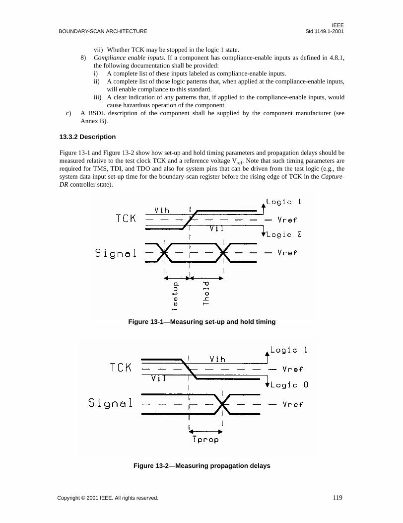
CAUTION: The descriptive material contained in this standard is for illustrative purposes only and does notdefine a preferred implementation. Examples are provided throughout this standard to illustrate possiblecircuit implementations. Where discrepancies between examples and specifications may occur, thespecifications always take precedence. Readers should exercise caution when using these examples toensure full compliance in their specific applications. In particular, it is emphasized that the examples aredesigned to effectively communicate the meaning of this standard. As such, they are logically correct;however, as always, a particular implementation may not operate properly with respect to timing and otherparametric characteristics. One example of this concern is that the sample TAP controller implementationdepicted in Figure 6-5 reasonably assumes a significantly greater delay in the flip-flop sourcing A and A*than in the inverter sourcing TCK*. It is possible to design a circuit where this assumption is violated,causing a critical race to occur that would invalidate the behavior of the TAP controller. Therefore, it isrecommended that implementations be fully verified to ensure compliance under required operatingconditions.
IEEEStd 1149.1-2001 IEEE STANDARD TEST ACCESS PORT AND
The following conventions are used in this standard:
a) The rules, recommendations, and permissions in each Specifications subclause are contained in asingle alphabetically indexed list. References to each rule, recommendation, or permission areshown in the form:
15.1.1 c) 2)| | |
Subclause number | |Index |
Option (if any)
b) Instruction and state names defined in this standard are shown in italic type in the text of this stan-dard.
c) Names of states and signals that pertain to the test data registers defined by this standard contain thecharacters DR, while those that pertain to the instruction register contain the characters IR.
d) Names for signals that are active in their low state have an asterisk as the final character, e.g.,TRST*.
e) A positive logic convention is used; i.e., a logic 1 signal is conveyed as the more positive of the twovoltages used for logic signals.
2. References
This standard shall be used in conjunction with the following standards. When the following standards aresuperseded by an approved revision, the revision shall apply.
EIA/JEP106, JEDEC Publication 106, Standard Manufacturer’s Identification Code1
IEEE 100, The Authoritative Dictionary of IEEE Standards Terms, Seventh Edition2
IEEE Std 1076-1993, IEEE Standard VHDL Language Reference Manual
IEEE Std 1149.4-1999, IEEE Standard for a Mixed Signal Test Bus
3. Definitions and Acronyms
For the purposes of this standard, the following terms and definitions apply. IEEE 100, The AuthoritativeDictionary of IEEE Standards Terms, Seventh Edition should be referenced for terms not defined in thisclause.
3.1 Definitions
3.1.1 active: When associated with a logic level (e.g., active-low), this term identifies the logic level towhich a signal shall be set to cause the defined action to occur. When referring to an output driver (e.g., anactive drive), this term describes the state in which the driver is capable of determining the voltage of thenetwork to which it is connected.
1Copies can be obtained from EIA/JEDEC, 2500 Wilson Blvd., Arlington, VA 22201-3834, USA (www.jedec.org).2IEEE publications are available from the Institute of Electrical and Electronics Engineers, 445 Hoes Lane, P.O. Box 1331, Piscataway,NJ 08855-1331, USA (http://standards.ieee.org/).
3.1.2 bidirectional pin: A component pin that can either drive or receive signals from external connections.
3.1.3 blind interrogation: Access to a facility (e.g., the device identification register) without priorknowledge of the test logic operation of the specific component being accessed.
3.1.4 built-in logic block observer (BILBO): A shift-register based structure used in some forms of self-testing circuit design.
3.1.5 capture: Load a value into a data register or the instruction register as a consequence of entry into theCapture-DR or Capture-IR controller state, respectively.
3.1.6 chip-on-board testing: A test of a component after it has been assembled onto a printed circuit boardor other substrate.
3.1.7 clock: A signal where transitions between the low and high logic levels (or vice versa) are used toindicate when a stored-state device, such as a flip-flop or latch, may perform an operation.
3.1.8 falling edge: A transition from a high to a low logic level. In positive logic, a change from logic 1 tologic 0. Events that are specified to occur on the rising (falling) edge of a signal should be completed withina fixed (frequency-independent) delay specified by the component supplier.
3.1.9 high: The higher of the two voltages used to convey a single bit of information. For positive logic, alogic 1.
3.1.10 inactive: When referring to an output driver (e.g., an inactive drive), this term describes the state inwhich the driver is not capable of determining the voltage of the network to which it is connected.
3.1.11 input pin: A component pin that receives signals from an external connection.
3.1.12 instruction: A binary data word shifted serially into the test logic in order to define its subsequentoperation.
3.1.13 least significant bit (LSB): The digit in a binary number representing the lowest numerical value.For shift-registers, the bit located nearest to the serial output, or the first bit to be shifted out. The leastsignificant bit of a binary word or shift-register is numbered 0.
3.1.14 level-sensitive scan design (LSSD): A variant of the scan design technique that results in race-free,testable digital electronic circuits.
3.1.15 low: The lower of the two voltages used to convey a single bit of information. For positive logic, alogic 0.
3.1.16 most significant bit (MSB): The digit in a binary number representing the greatest numerical value.For shift-registers, the bit farthest from the serial output, or the last bit to be shifted out. Logic valuesexpressed in binary form are shown with the most significant bit on the left.
3.1.17 nonclock: A signal where the transitions between the low and high logic levels do not themselvescause operation of stored-state devices. The logic level is important only at the time of a transition on a clocksignal.
3.1.18 output pin: A component pin that drives signals onto external connections.
IEEEStd 1149.1-2001 IEEE STANDARD TEST ACCESS PORT AND
3.1.19 pin: The point at which connection is made between the integrated circuit and the substrate on whichit is mounted (e.g., the printed circuit board). For packaged components, this would be the package pin; forcomponents mounted directly on the substrate, this would be the bonding pad.
3.1.20 prime source: In the event that several vendors offer pin-for-pin compatible components, the primesource is the vendor that introduced the component type.
3.1.21 private: A design feature intended solely for use by the component manufacturer.
3.1.22 public: A design feature, documented in the component data sheet, that may be used by purchasersof the component.
3.1.23 reset: The establishment of an initial logic condition that can be either logic 0 or logic 1, asdetermined by the context.
3.1.24 rising edge: A transition from a low to a high logic level. In positive logic, a change from logic 0 tologic 1. Events that are specified to occur on the rising (falling) edge of a signal should be completed withina fixed (frequency-independent) delay specified by the component supplier.
3.1.25 scan design: A design technique that introduces shift-register paths into digital electronic circuitsand thereby improves their testability.
3.1.26 scan path: The shift-register path through a circuit designed using the scan design technique.
3.1.27 second source: In the event that several vendors offer pin-for-pin compatible components, second-source suppliers are vendors of the component other than the prime source.
3.1.28 selected test data register: A test data register is selected when it is required to operate by aninstruction supplied to the test logic.
3.1.29 signature analysis: A technique for compressing a sequence of logic values output from a circuitunder test into a small number of bits of data (signature) that, when compared to stored data, will indicate thepresence or absence of faults in the circuit.
3.1.30 stand-alone testing: A test of a component performed before it is assembled onto a board or othersubstrate, for example, using Automatic Test Equipment (ATE).
3.1.31 stuck-at fault: A failure in a logic circuit that causes a signal connection to be fixed at 0 or 1 regard-less of the operation of the circuitry that drives it.
3.1.32 system: Pertaining to the nontest function of the circuit.
3.1.33 system logic: Any item of logic that is dedicated to realizing the nontest function of the componentor is at the time of interest configured to achieve some aspect of the nontest function.
3.1.34 system pin: A component pin that feeds, or is fed from, the on-chip system logic.
3.1.35 test logic: Any item of logic that is a dedicated part of the test logic architecture or is at the time ofinterest configured as a part of the test logic architecture.
3.1.36 update: Transfer of a logic value from the shift-register stage of a data register cell or an instructionregister cell into the latched parallel output stage of the cell as a consequence of the falling edge of the testclock input in the Update-DR or Update-IR controller state, respectively.
3.1.37 3-state pin: A component output pin where the drive may be either active or inactive (for example, athigh impedance).
3.2 Acronyms
ATE automatic test equipmentBILBO built-in logic block observerLSB least significant bitLSSD level-sensitive scan design MSB most significant bit TAP test access port (see Clause 4)TCK test clock input (see 4.2)TDI test data input (see 4.4)TDO test data outputs (see 4.5)TMS test mode select (see 4.3)TRST* test reset (see 4.6)TTL transistor transistor logic
4. Test access port (TAP)
The TAP is a general-purpose port that can provide access to many test support functions built into acomponent, including the test logic defined by this standard. It is composed as a minimum of the three inputconnections and one output connection required by the test logic defined by this standard. An optional fourthinput connection provides for asynchronous initialization of the test logic defined by this standard.
4.1 Connections that form the test access port (TAP)
4.1.1 Specifications
Rules
a) The TAP shall include the following connections (defined in 4.2, 4.3, 4.4, and 4.5): TCK, TMS,TDI, and TDO.
b) Where the TAP controller is not reset at power-up as a result of features built into the test logic, aTRST* input shall be provided as defined in 4.6 (see also 6.3).
c) All TAP inputs and outputs shall be dedicated connections to the component (i.e., the pins used shallnot be used for any other purpose).
4.1.2 Description
Dedicated TAP connections are required to allow access to the full range of mandatory features of thisstandard.
4.2 Test clock input (TCK)
The test clock input (TCK) provides the clock for the test logic defined by this standard.
IEEEStd 1149.1-2001 IEEE STANDARD TEST ACCESS PORT AND
a) Stored-state devices contained in the test logic shall retain their state indefinitely when the signalapplied to TCK is stopped at 0.
Recommendations
b) Since TCK inputs for many components may be controlled from a single driver, care should betaken to ensure that the load presented by TCK is as small as possible.
Permissions
c) Stored-state devices contained in the test logic may retain their state indefinitely when the signalapplied to TCK is stopped at 1.
4.2.2 Description
The dedicated TCK input is included so that the serial test data path between components can be usedindependently of component-specific system clocks, which may vary significantly in frequency from onecomponent to the next. It also permits shifting of test data concurrently with normal system operation of thecomponent. The latter facility is required to support the use of the TAP and test data registers in a design foron-line system monitoring. The provision of an independent clock ensures that test data can be moved to orfrom a chip without changing the state of the on-chip system logic. The independent clock is also essential ifboundary-scan registers are to be usable for board interconnect testing in all circumstances—including caseswhere system clock signals are derived in one component for use in others.
While TCK will in many cases be driven by a free-running clock with a nominal 50% duty cycle, there maybe situations where the clock needs to stop for a period. One example is when an ATE needs to fetch testdata from backup memory (e.g., disc), since some test systems are unable to keep the clock running duringsuch an operation. This standard requires that TCK can be stopped at 0 indefinitely without causing anychange to the state of the test logic. While the TCK signal is stopped at 0, stored-state devices are required toretain their state so that the test logic may continue its operation when clock operation restarts. Optionally, acomponent also may allow TCK to be stopped at 1 for an indefinite period.
Many parts of the test logic perform operations in response to the rising or falling edge of TCK, as indicatedby the use of the phrase “on the rising (falling) edge of TCK.” These operations have to be completed withina fixed (frequency-independent) delay after the occurrence of the relevant change at TCK, and this delay hasto be specified by the component supplier. Therefore, the phrase “on the rising (falling) edge of TCK”should be interpreted as “within a specified delay after the rising (falling) edge of TCK.”
NOTE—In many applications, the TCK signal applied to components that conform to this standard will have a dutycycle close to 50% (i.e., the periods that the clock spends at 0 and 1 will be equal) at a given frequency. It is expected thatall propagation delays will be such that correct operation is achieved under these circumstances (50% duty cycle at agiven TCK frequency), particularly when data is being transferred between TDO of one chip and TDI of another.
4.3 Test mode select input (TMS)
The signal received at TMS is decoded by the TAP controller to control test operations.
4.3.1 Specifications
Rules
a) The signal presented at TMS shall be sampled by the test logic on the rising edge of TCK.b) The design of the circuitry fed from TMS shall be such that an undriven input produces a logical
response identical to the application of a logic 1.
Recommendations
c) Since the TMS inputs for many components may be controlled from a single driver, care should betaken to ensure that the load presented by TMS is as small as possible.
4.3.2 Description
Rule 4.3.1 b) is included so that the TAP controller is forced into the Test-Logic-Reset controller state in thecase of an undriven TMS pin. This ensures that normal operation of the complete design can continue with-out interference from the test logic (see 6.3). For TTL-compatible designs, the rule may be met by includinga pull-up resistor in the component's TMS input circuitry.
Signal values presented at TMS are sampled by the test logic on the rising edge of TCK. It is expected thatthe bus master (ATE, bus controller, etc.) will change the signal driven to the TMS inputs of connectedcomponents on the falling edge of TCK. The waveforms shown elsewhere in this standard reflect thisexpectation.
4.4 Test data input (TDI)
Serial test instructions and data are received by the test logic at TDI.
4.4.1 Specifications
Rules
a) The signal presented at TDI shall be sampled into the test logic on the rising edge of TCK.b) The design of the circuitry fed from TDI shall be such that an undriven input produces a logical
response identical to the application of a logic 1.c) When data is being shifted from TDI toward TDO, test data received at TDI shall appear without
inversion at TDO after a number of rising and falling edges of TCK determined by the length of theinstruction or test data register selected.
IEEEStd 1149.1-2001 IEEE STANDARD TEST ACCESS PORT AND
The data pins (TDI and TDO) provide for serial movement of test data through the circuit. The requirementfor data to be propagated from TDI to TDO without inversion is included to simplify the operation of com-ponents compatible with this standard linked on a printed circuit board.
Values presented at TDI are clocked into the selected register (instruction or test data) on a rising edge ofTCK. It is expected that the bus master (ATE, bus controller, etc.) will change the signal driven to the TDIinput of the first component on a serial board-level path on the falling edge of TCK. The waveforms shownelsewhere in this standard reflect this expectation.
Rule 4.4.1 b) is included so that open-circuit faults in the board-level serial test data path cause a definedlogic value to be shifted into the test logic. Note that when this constant value is shifted into the instructionregister, the bypass register will be selected (as will be discussed further in 8.4). For TTL-compatibledesigns, this rule may be met by inclusion of a pull-up resistor in the component's TDI input circuitry.
4.5 Test data output (TDO)
TDO is the serial output for test instructions and data from the test logic defined in this standard.
4.5.1 Specifications
Rules
a) Changes in the state of the signal driven through TDO shall occur only on the falling edge of TCK.b) The TDO driver shall be set to its inactive drive state except when the scanning of data is in progress
(see 6.2).
4.5.2 Description
To ensure race-free operation, changes on TAP inputs (TMS and TDI) are clocked into the test logic definedby this standard on the rising edge of TCK while changes at the TAP output (TDO) occur on the falling edgeof TCK. Similarly, for test logic able to drive or receive signals from system pins (e.g., the boundary-scanregister), signals driven out of the component from the test logic change state on the falling edge of TCK,while those entering the test logic are clocked in on the rising edge (as will be discussed in 9.3).
The contents of the selected register (instruction or data) are shifted out of TDO on the falling edge of TCK.In the illustrations given in this document, edge-operated circuit designs generally are used. For an edge-operated implementation, note that the TDO output changes shall be delayed until the falling edge of TCK,which can be achieved by including a flip-flop clocked by the falling edge of TCK in the TDO output buffer.Where the registers are constructed from master and slave latches controlled by nonoverlapping clocks, theretiming required by Rule 4.5.1 a) is an inherent feature of the design.
The ability of TDO to switch between active and inactive drive is required to allow parallel, rather thanserial, connection of board-level test data paths in cases where this is required. In TTL or CMOS technolo-gies, for example, this requirement may be met through use of a 3-state output buffer.
4.6 Test reset input (TRST*)
The optional TRST* input provides for asynchronous initialization of the TAP controller (see 6.3).
a) If TRST* is included in the TAP, the TAP controller shall be asynchronously reset to the Test-Logic-Reset controller state when a logic 0 is applied to TRST* (see 6.3).
NOTE—As a result of this event, all other test logic in the component is asynchronously reset to the state required in theTest-Logic-Reset controller state.
b) If TRST* is included in the TAP, the design of the circuitry fed from that input shall be such that anundriven input produces a logical response identical to the application of a logic 1.
c) TRST* shall not be used to initialize any system logic within the component.
Recommendations
d) To ensure deterministic operation of the test logic, TMS should be held at 1 while the signal appliedat TRST* changes from 0 to 1.
4.6.2 Description
Initialization of the TAP controller in turn causes asynchronous initialization of other test logic included inthe design, as discussed in the subsequent clauses of this standard.
Rule 4.6.1 b) is included to ensure that in the case of an unterminated TRST* input, test logic operation canproceed under control of signals applied at the TMS and TCK inputs. For TTL-compatible designs, this rulemay be met by inclusion of a pull-up resistor in the TRST* input circuitry of the component.
Rule 4.6.1 c) ensures that the test logic can be reset independently of the on-chip system logic. This allowsthe test logic to be disabled by hard-wiring TRST* to logic 0.
Recommendation 4.6.1 d) is included to ensure that the test logic responds predictably when the signalapplied to TRST* changes from 0 to 1. If rising edges occur simultaneously at TRST* and TCK when alogic 0 is applied to TMS, a race will occur, and the TAP controller may either remain in the Test-Logic-Reset controller state or enter the Run-Test/Idle controller state.
4.7 Interconnection of components compatible with this standard
4.7.1 Specifications
Permissions
a) The TAP input and output connections may be interconnected at the board level in a manner appro-priate to the assembled product.
4.7.2 Description
Figure 4-1, Figure 4-2, and Figure 4-3 illustrate three alternative board-level interconnections ofcomponents conforming to this standard.
In each example, the test bus may be controlled either by an ATE system or by a component that provides aninterface to a test bus at the next level of product assembly (for example, at the board/backplane interface).In this standard, the device that controls the board-level test bus is referred to as the bus master.
IEEEStd 1149.1-2001 IEEE STANDARD TEST ACCESS PORT AND
Note that the minimum configuration (shown in Figure 4-1) contains
— Two broadcast signals (TMS and TCK) fed from the testability bus master to all slaves in parallel;and
— A serial path formed by a daisy-chain connection of the serial test data pins (TDI and TDO).
The hybrid serial/parallel connection shown in Figure 4-2 uses a pair of coordinated TMS signals (TMS1and TMS2) to ensure that only one serial path is scanning data at a given time. This configuration makes useof the 3-state feature of the TDO output pin, which ensures that only the components that are scanning datahave TDO in the active drive state.
Figure 4-3 shows the four components connected to give four separate serial paths through the completeboard design. These paths have separate TDI and TDO signals but can be controlled from common TCK andTMS signals.
When choosing a configuration for the board-level interconnection of components conforming to thisstandard, it is necessary to consider the capability of test equipment and test pattern generators. It is fullyexpected that any test equipment and/or test pattern generators that intend to support a test methodologybased on the boundary-scan architecture defined by this standard would be able to test the board-levelconfiguration of Figure 4-1, since the degenerate form of this configuration is a single conformantcomponent. On the other hand, some test equipment and/or test pattern generators may not be able to test theboard-level configurations of Figure 4-2 and Figure 4-3.
Figure 4-1—Serial connection using one TMS signal
Figure 4-2—Connection in two paralleled serial chains
4.8 Subordination of this standard within a higher-level test strategy
While the test logic specified by this standard has been designed to be extensible to meet the particular needsof individual designers or companies (for example, by the flexibility of the instruction register), occasionsmay arise when it will be desirable to terminate compliance with this standard by a component temporarilyand enable complementary test functionality. An example (illustrated in Annex A) involves a Level-Sensi-tive Scan Design (LSSD) infrastructure required for use during “stand-alone'' component testing, which can-not be simultaneously operated with the test functionality defined by this standard (which is required tosupport testing of boards onto which the components implementing the two testing techniques will beassembled).
This subclause defines how compliance with this standard may be “switched on” or “switched off.” Therules require the change of test functionality to be under the control of signals applied at one or morecomponent pins. Compliance has to be effected by a single logic pattern applied at these pins, not by asequence of such patterns.
4.8.1 Specifications
Rules
a) If a component is to be designed having both1) Test functionality compliant with this standard; and2) Other test functionality that is not to be controlled via the test circuitry and the means of control
defined in this standard,
compliance with this standard shall be enabled/disabled by one or more steady-state logic patterns (called“compliance-enable” patterns) applied at a fixed set of component inputs, to be called “compliance-enableinputs.”
NOTE—The steady-state combinational logic pattern may be chosen from a set of such “compliance-enable” patterns,all of which have equivalent effect [see Permission 4.8.1 h)].
Figure 4-3—Multiple independent paths with common TMS and TCK signals
IEEEStd 1149.1-2001 IEEE STANDARD TEST ACCESS PORT AND
b) Any one of the compliance-enable patterns, when applied to the compliance-enable inputs withoutregard to preceding patterns on these inputs, shall cause the component to be fully compliant withthis standard.
c) Once compliance with this standard is established by the application of a compliance-enable patternat the compliance-enable inputs, compliance to this standard shall be maintained continuously untilthe logic pattern applied at the compliance-enable inputs ceases to be a compliance-enable pattern.
NOTES
1—This rule implies that transition between compliance-enable patterns must produce no untoward effects on compli-ance. Limiting the number of compliance-enable patterns is one way to prevent problems from arising.
2—The rules in other subclauses of this standard apply only when compliance is enabled. Therefore, where compliance-enable inputs are provided, each rule should be considered to be prefaced by “When compliance to this standard isenabled, ....” For example, Rule 4.1.1 c) should be read as stipulating that the TAP pins are dedicated connections andmay not be used for any other purpose while compliance to this standard is enabled. When compliance is disabled, theTAP connections may be reused, for example, to provide controls for an alternative test mode of component operation.
3—The event of enabling compliance with this standard by changing the logic pattern applied at the compliance-enableinputs of a component need not have an effect on the component equivalent to that of power-up of the component.
d) Compliance-enable inputs shall be dedicated inputs to the component and shall not be used for anyother purpose.
Recommendations
e) The number of compliance-enable inputs provided on a component should be minimized.
Permissions
f) A component may have zero, one, or more compliance-enable inputs.g) If a component with compliance-enable input(s) has a TRST* line included in its TAP
implementation, the design of the component may require that the TRST* input be driven low at thetime of application of a compliance-enable pattern in order to achieve reset of the relevant test logicconcurrent with the operation of that test logic.
h) A component may have several compliance-enable patterns, all of which have an equivalent effect.
4.8.2 Description
If compliance-enable inputs are provided, there shall exist at least one logic pattern that, when applied at thecompliance-enable inputs, will result in the component becoming fully compliant with this standard.
5. Test logic architecture
This clause defines the top-level design of the test logic accessed through the TAP. Detailed designrequirements for the various blocks contained within the test logic design are contained in the subsequentclauses of this standard.
a) The following elements shall be contained in the test logic architecture:1) A TAP (see Clause 4);2) A TAP controller (see Clause 6);3) An instruction register (see Clause 7); and4) A group of test data registers (see Clause 9).
b) The instruction and test data registers shall be separate shift-register based paths that are connectedin parallel and have a common serial data input and a common serial data output connected to theTAP TDI and TDO signals, respectively.
c) The selection between the alternative instruction and test data register paths between TDI and TDOshall be made under the control of the TAP controller, as defined in 6.2.
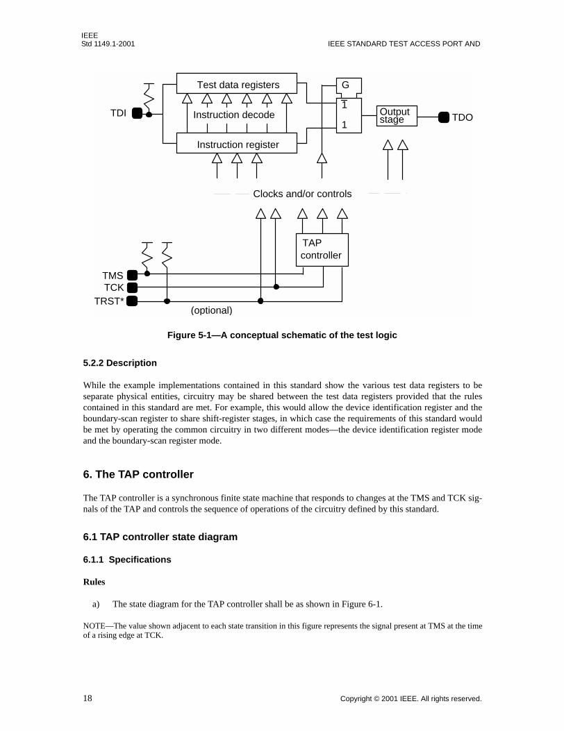
5.1.2 Description
A conceptual view of the top-level design of the test logic architecture defined by this standard is shown inFigure 5-1. This figure and the others included in the descriptive material contained in this standard areexamples intended only to illustrate a possible embodiment of this standard. These figures do not indicate apreferred implementation.
Key features of the design are as follows:
a) The TAP controller. This receives TCK and interprets the signals on TMS. The TAP controller gen-erates clock or control signals or both as required for the instruction and test data registers and forother parts of the architecture. The specification for the TAP controller is contained in Clause 6.
b) The instruction register. This allows the instruction to be shifted into the design. The instruction isused to select the test to be performed or the test data register to be accessed or both. Thespecification for the instruction register is contained in Clause 7.
c) The group of test data registers. The group of test data registers shall include a bypass and a bound-ary-scan register. It also may include an optional device identification register and further optionaltest data registers. Further information on the structure of the group of test data registers is containedin Clause 9.
Note that, depending on the style of implementation of the test logic defined by this standard, circuitry maybe required, in the output stage shown in Figure 5-1, to retime the signal passing through it to occur on thefalling edge of TCK.
5.2 Test logic realization
5.2.1 Specifications
Rules
a) The TAP controller, the instruction register, and the associated circuitry necessary for control of theinstruction and test data registers shall be dedicated test logic (i.e., these test logic blocks shall notperform any system function).
b) If test access is required to a test data register without causing any interference to the operation ofthe on-chip system logic, the circuitry used to construct that test data register shall be dedicated testlogic.
IEEEStd 1149.1-2001 IEEE STANDARD TEST ACCESS PORT AND
While the example implementations contained in this standard show the various test data registers to beseparate physical entities, circuitry may be shared between the test data registers provided that the rulescontained in this standard are met. For example, this would allow the device identification register and theboundary-scan register to share shift-register stages, in which case the requirements of this standard wouldbe met by operating the common circuitry in two different modes—the device identification register modeand the boundary-scan register mode.
6. The TAP controller
The TAP controller is a synchronous finite state machine that responds to changes at the TMS and TCK sig-nals of the TAP and controls the sequence of operations of the circuitry defined by this standard.
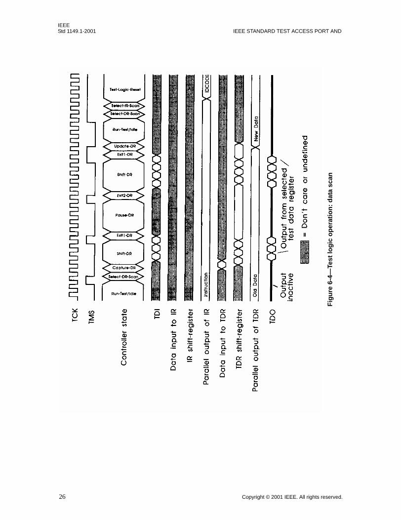
6.1 TAP controller state diagram
6.1.1 Specifications
Rules
a) The state diagram for the TAP controller shall be as shown in Figure 6-1.
NOTE—The value shown adjacent to each state transition in this figure represents the signal present at TMS at the timeof a rising edge at TCK.
Figure 5-1—A conceptual schematic of the test logic
b) All state transitions of the TAP controller shall occur based on the value of TMS at the time of a ris-ing edge of TCK.
c) Actions of the test logic (instruction register, test data registers, etc.) shall occur on either the risingor the falling edge of TCK in each controller state, as shown in Figure 6-2.
6.1.2 Description
The behavior of the TAP controller and other test logic in each of the controller states is briefly described asfollows. Rules governing the behavior of the test logic defined by this standard in each controller state arecontained in later clauses of this standard.
Figure 6-1—TAP controller state diagram
Figure 6-2—Timing of actions in a controller state
IEEEStd 1149.1-2001 IEEE STANDARD TEST ACCESS PORT AND
The test logic is disabled so that normal operation of the on-chip system logic (i.e., in response to stimulireceived through the system pins only) can continue unhindered. This is achieved by initializing the instruc-tion register to contain the IDCODE instruction or, if the optional device identification register is not pro-vided, the BYPASS instruction (see 7.2). No matter what the original state of the controller, it will enter Test-Logic-Reset when TMS is held high for at least five rising edges of TCK. The controller remains in this statewhile TMS is high.
If the controller should leave the Test-Logic-Reset controller state as a result of an erroneous low signal onthe TMS line at the time of a rising edge on TCK (for example, a glitch due to external interference), it willreturn to the Test-Logic-Reset state after three rising edges of TCK with the TMS line at the intended highlogic level. The operation of the test logic is such that no disturbance is caused to on-chip system logic oper-ation as the result of such an error. On leaving the Test-Logic-Reset controller state, the controller moves intothe Run-Test/Idle controller state, where no action will occur because the current instruction has been set toselect operation of the device identification or bypass register (see 7.2). The test logic is also inactive in theSelect-DR-Scan and Select-IR-Scan controller states.
Note that the TAP controller will also be forced to the Test-Logic-Reset controller state by applying a lowlogic level at TRST*, if such is provided, or at power-up (see 6.3).
Run-Test/Idle
A controller state between scan operations. Once entered, the controller will remain in the Run-Test/Idlestate as long as TMS is held low. When TMS is high and a rising edge is applied at TCK, the controllermoves to the Select-DR-Scan state.
In the Run-Test/Idle controller state, activity in selected test logic occurs only when certain instructions arepresent. For example, the RUNBIST instruction causes a self-test of the on-chip system logic to execute inthis state (see 8.10). Self-tests selected by instructions other than RUNBIST also may be designed to executewhile the controller is in this state.
For instructions that do not cause functions to execute in the Run-Test/Idle controller state, all test data regis-ters selected by the current instruction shall retain their previous state (i.e., Idle).
The instruction does not change while the TAP controller is in this state.
Select-DR-Scan
This is a temporary controller state in which all test data registers selected by the current instruction retaintheir previous state.
If TMS is held low and a rising edge is applied to TCK when the controller is in this state, the controllermoves into the Capture-DR state and a scan sequence for the selected test data register is initiated. If TMS isheld high and a rising edge is applied to TCK, the controller moves on to the Select-IR-Scan state.
The instruction does not change while the TAP controller is in this state.
Select-IR-Scan
This is a temporary controller state in which all test data registers selected by the current instruction retaintheir previous state.
If TMS is held low and a rising edge is applied to TCK when the controller is in this state, then the controllermoves into the Capture-IR state and a scan sequence for the instruction register is initiated. If TMS is heldhigh and a rising edge is applied to TCK, the controller returns to the Test-Logic-Reset state.
The instruction does not change while the TAP controller is in this state.
Capture-DR
In this controller state data may be parallel-loaded into test data registers selected by the current instructionon the rising edge of TCK. If a test data register selected by the current instruction does not have a parallelinput, or if capturing is not required for the selected test, the register retains its previous state unchanged.
The instruction does not change while the TAP controller is in this state.
When the TAP controller is in this state and a rising edge is applied to TCK, the controller enters either theExit1-DR state if TMS is held at 1 or the Shift-DR state if TMS is held at 0.
Shift-DR
In this controller state, the test data register connected between TDI and TDO as a result of the currentinstruction shifts data one stage toward its serial output on each rising edge of TCK. Test data registers thatare selected by the current instruction but are not placed in the serial path retain their previous stateunchanged.
The instruction does not change while the TAP controller is in this state.
When the TAP controller is in this state and a rising edge is applied to TCK, the controller either enters theExit1-DR state if TMS is held at 1 or remains in the Shift-DR state if TMS is held at 0.
Exit1-DR
This is a temporary controller state. If TMS is held high, a rising edge applied to TCK while in this statecauses the controller to enter the Update-DR state, which terminates the scanning process. If TMS is heldlow and a rising edge is applied to TCK, the controller enters the Pause-DR state.
All test data registers selected by the current instruction retain their previous state unchanged.
The instruction does not change while the TAP controller is in this state.
Pause-DR
This controller state allows shifting of the test data register in the serial path between TDI and TDO to betemporarily halted. All test data registers selected by the current instruction retain their previous stateunchanged.
The controller remains in this state while TMS is low. When TMS goes high and a rising edge is applied toTCK, the controller moves on to the Exit2-DR state.
The instruction does not change while the TAP controller is in this state.
IEEEStd 1149.1-2001 IEEE STANDARD TEST ACCESS PORT AND
This is a temporary controller state. If TMS is held high and a rising edge is applied to TCK while in thisstate, the scanning process terminates and the TAP controller enters the Update-DR controller state. If TMSis held low and a rising edge is applied to TCK, the controller enters the Shift-DR state.
All test data registers selected by the current instruction retain their previous state unchanged.
The instruction does not change while the TAP controller is in this state.
Update-DR
Some test data registers may be provided with a latched parallel output to prevent changes at the parallel out-put while data is shifted in the associated shift-register path in response to certain instructions (e.g., EXTEST,INTEST, and RUNBIST). Data is latched onto the parallel output of these test data registers from the shift-register path on the falling edge of TCK in the Update-DR controller state. The data held at the latched par-allel output should not change other than in this controller state unless operation during the execution of aself-test is required (e.g., during the Run-Test/Idle controller state in response to a design-specific publicinstruction).
All shift-register stages in test data registers selected by the current instruction retain their previous stateunchanged.
The instruction does not change while the TAP controller is in this state.
When the TAP controller is in this state and a rising edge is applied to TCK, the controller enters either theSelect-DR-Scan state if TMS is held at 1 or the Run-Test/Idle state if TMS is held at 0.
Capture-IR
In this controller state the shift-register contained in the instruction register loads a pattern of fixed logic val-ues on the rising edge of TCK. In addition, design-specific data may be loaded into shift-register stages thatare not required to be set to fixed values (see Clause 7).
Test data registers selected by the current instruction retain their previous state. The instruction does notchange while the TAP controller is in this state.
When the TAP controller is in this state and a rising edge is applied to TCK, the controller enters either theExit1-IR state if TMS is held at 1 or the Shift-IR state if TMS is held at 0.
Shift-IR
In this controller state the shift-register contained in the instruction register is connected between TDI andTDO and shifts data one stage toward its serial output on each rising edge of TCK.
Test data registers selected by the current instruction retain their previous state. The instruction does notchange while the TAP controller is in this state.
When the TAP controller is in this state and a rising edge is applied to TCK, the controller either enters theExit1-IR state if TMS is held at 1 or remains in the Shift-IR state if TMS is held at 0.
This is a temporary controller state. If TMS is held high, a rising edge applied to TCK while in this statecauses the controller to enter the Update-IR state, which terminates the scanning process. If TMS is held lowand a rising edge is applied to TCK, the controller enters the Pause-IR state.
Test data registers selected by the current instruction retain their previous state. The instruction does notchange while the TAP controller is in this state and the instruction register retains its state.
Pause-IR
This controller state allows shifting of the instruction register to be halted temporarily.
Test data registers selected by the current instruction retain their previous state. The instruction does notchange while the TAP controller is in this state and the instruction register retains its state.
The controller remains in this state while TMS is low. When TMS goes high and a rising edge is applied toTCK, the controller moves on to the Exit2-IR state.
Exit2-IR
This is a temporary controller state. If TMS is held high and a rising edge is applied to TCK while in thisstate, termination of the scanning process results, and the TAP controller enters the Update-IR controllerstate. If TMS is held low and a rising edge is applied to TCK, the controller enters the Shift-IR state.
Test data registers selected by the current instruction retain their previous state. The instruction does notchange while the TAP controller is in this state and the instruction register retains its state.
Update-IR
The instruction shifted into the instruction register is latched onto the parallel output from the shift-registerpath on the falling edge of TCK in this controller state. Once the new instruction has been latched, itbecomes the current instruction.
Test data registers selected by the current instruction retain their previous state.
When the TAP controller is in this state and a rising edge is applied to TCK, the controller enters the Select-DR-Scan state if TMS is held at 1 or the Run-Test/Idle state if TMS is held at 0.
The Pause-DR and Pause-IR controller states are included so that shifting of data through the test data orinstruction register can be halted temporarily. For example, this might be necessary in order to allow an ATEsystem to reload its pin memory from disc during application of a long test sequence. Boundary-scan testsequences are likely to extend to the order of 107 test patterns for complex board designs.
The TAP controller states include the three basic actions required for testing: stimulus application (Update-DR), execution (Run-Test/Idle), and response capture (Capture-DR). However, not all these actions arerequired for every type of test. Table 6-1 lists the actions required for key types of test supported by thisstandard.
For scan testing, the stimulus is made available for use at the end of shifting or, if a parallel output latch isincluded, by updating the parallel output in the Update-DR controller state. The results of the test are cap-tured into the test data register during the Capture-DR controller state.
IEEEStd 1149.1-2001 IEEE STANDARD TEST ACCESS PORT AND
For internally controlled self-testing circuit designs, the starting values of the registers are available at theend of shifting: there is no parallel output latch to update. The registers should operate under control of theinternal test logic during Run-Test/Idle. Since the result is already contained in a test data register, no actionis required during the Capture-DR controller state.
For an internal scan test, the target register consists of a serial concatenation of storage elements that supportthe normal system operation of the component. The construction of such a register is beyond the scope ofthis standard, and parallel output latches may or may not be present in a given implementation.
6.2 TAP controller operation
6.2.1 Specifications
Rules
a) The TAP controller shall change state only in response to the following events:1) A rising edge of TCK;2) A transition to logic 0 at the TRST* input (if provided); or3) Power-up.
b) The TAP controller shall generate signals to control the operation of the test data registers, instruc-tion registers, and associated circuitry as defined in this standard (Figure 6-3 and Figure 6-4).
NOTE—In these figures, the assumption is made that the signals applied to TMS and TDI change state on the fallingedge of TCK. The time at which these signals change state is not defined by this standard, but it should be such that theset-up and hold requirements of TMS and TDI are met. It is further assumed that the design includes the optional deviceidentification register. Therefore, the figures show the IDCODE instruction being set onto the output of the instructionregister in the Test-Logic-Reset controller state. If the device identification register is not included in the design, the out-put of the instruction register will be set to the BYPASS instruction in the Test-Logic-Reset controller state.
c) The TDO output buffer and the circuitry that selects the register output fed to TDO shall be con-trolled as shown in Table 6-2.
d) Changes at TDO defined in Table 6-2 shall occur on the falling edge of TCK after entry into thestate.
Table 6-1—Use of controller states for different test types
Test typeAction required in this controller state
Update-DR Run-Test/Idle Capture-DR
Boundary-scan external test (e.g., EXTEST) Yes No Yes
Boundary-scan internal scan test (e.g., INTEST) Maybe Maybe Yes
Boundary-scan PRELOAD Yes No Maybe
Boundary-scan SAMPLE Maybe No Yes
Internally controlled built-in tests (e.g., RUNBIST) No Yes No
Internal scan test (i.e., a specific user-defined PUBLIC instruction)
NOTE—Some components designed before publication of this standard may conform in every respect except that theyhave TDO active in the Capture-IR, Pause-IR, Exit1-IR, Exit2-IR, Capture-DR, Pause-DR, Exit1-DR, and Exit2-DR con-troller states, in addition to the Shift-IR and Shift-DR controller states. The functionality of these components is indistin-guishable from that of components that fully conform to this standard except where the TDO output of such a componentis connected to the TDO output of another (e.g., as shown in Figure 4-2).
6.2.2 Description
An example of a circuit that meets the requirements of 6.2.1 is shown in Figure 6-5 and Figure 6-6. Thiscircuit generates a range of clock and control signals required not only to control the selection between thealternative instruction and test data register paths and the activity of TDO (as defined in Table 6-2) but alsoto control the example implementations of other items of test logic that are contained in this standard.
The assignment of controller states in the example implementation is given in Table 6-3.
The Boolean equations for the next state logic in Figure 6-5 and Figure 6-6 are as follows:
Figure 6-5—A TAP controller implementation—state registers and output logic
NOTE—The circuit in Figure 6-5 generates the various control signals used by the example circuits illustrated elsewherein this standard. Note that the Select signal would be used to control the multiplexer shown in Figure 5-1 and the Enablesignal would be used for 3-state control of the TDO output. Note also that while the ShiftDR and ClockDR signals maybe broadcast to all test data registers, distribution of the UpdateDR control signal will be controlled according to theinstruction held in the instruction register such that the signal is fed only to the test data register that is selected as theserial path between TDI and TDO.
a) The TAP controller shall be forced into the Test-Logic-Reset controller state at power-up either byuse of the TRST* signal or as a result of circuitry built into the test logic.
NOTE—If the TAP controller is to be reset at power-up using TRST*, the design of the assembled system has to ensurethat a logic 0 is applied to TRST* when power is applied. Similarly, where the TAP controller is to be reset using TRST*after enabling of compliance to this standard as described in 4.8, the design of the assembled system has to ensure that alogic 0 is applied to TRST* when compliance is enabled.
b) The TAP controller shall not be initialized by the operation of any system input, such as a systemreset.
c) Where a dedicated reset pin (TRST*) is provided to allow initialization of the TAP controller,initialization shall occur asynchronously when the TRST* input changes to the low logic level.
Table 6-3—State assignments for example TAP controller
Controller State DCBA (hex)
Exit2-DR 0
Exit1-DR 1
Shift-DR 2
Pause-DR 3
Select-IR-Scan 4
Update-DR 5
Capture-DR 6
Select-DR-Scan 7
Exit2-IR 8
Exit1-IR 9
Shift-IR A
Pause-IR B
Run-Test/Idle C
Update-IR D
Capture-IR E
Test-Logic-Reset F
IEEEStd 1149.1-2001 IEEE STANDARD TEST ACCESS PORT AND
d) Where the TAP controller is initialized at power-up by operation of circuitry built into the test logic,the result shall be equivalent to that which would be achieved by application of a logic 0 to a TRST*input.
6.3.2 Description
In a board design that contains wired junctions or buses, provision shall be made to ensure that at power-upany period of contention between drivers on the bus is kept within limits that ensure that no damage occursto the components on the board.
When boundary-scan circuitry is inserted between the on-chip system logic and package pins, it becomesessential to ensure that shortly after power-up this circuitry enters a state where buses and wired junctionsare controlled by the system circuitry, i.e., the Test-Logic-Reset controller state.
NOTE—Clause 11 contains rules that ensure that boundary-scan circuitry at system pins does not interfere with normalsystem operation when the Test-Logic-Reset controller state is selected.
While the TAP controller will synchronously enter the Test-Logic-Reset controller state after five risingedges at TCK (provided that TMS is held high), the worst-case time taken to reach this state may exceed thatat which damage could occur. Further, it cannot be guaranteed that the clock will be running at the time atwhich power is applied to the board. Therefore, the “reset at power-up” requirement is included.
The requirement can be met in a variety of ways, for example, by inclusion of a power-up reset within theintegrated circuit or by asymmetric design of the latches or registers used to construct the TAP controller. Italso could be met by inclusion of a dedicated TRST* pin for the TAP controller. However, a system resetcannot also be used to initialize the TAP controller, since this would compromise the ability to test systeminterconnections at the board level using the boundary-scan circuitry. In some systems it also may be possi-ble to use the independence of the system and test resets to allow sampling and examination of data after asystem crash. This would require that the test logic be reset before reinitialization of the on-chip systemlogic.
Where a power-up reset facility is provided within the component, this can be used to initialize both the sys-tem and the test logic, for example, as shown in Figure 6-8.
Figure 6-8—Use of power-up reset for system and test logic
The instruction register allows an instruction to be shifted into the design. The instruction is used to selectthe test to be performed or the test data register to be accessed or both. As will be discussed in Clause 8, anumber of mandatory and optional instructions are defined by this standard. Further design-specific instruc-tions can be added to allow the functionality of the test logic built into a component to be extended.
Optionally, the instruction register allows examination of design-specific information generated within thecomponent.
This clause contains the design requirements for the instruction register.
7.1 Design and construction of the instruction register
The instruction register is a shift-register-based design that has an optional parallel input for register cellsother than the two nearest to the serial output. The instruction shifted into the register is latched at the com-pletion of the shifting process.
7.1.1 Specifications
Rules
a) The instruction register shall include at least two shift-register-based cells capable of holdinginstruction data.
b) The instruction shifted into the instruction register shall be latched such that changes in the effect ofan instruction occur only in the Update-IR and Test-Logic-Reset controller states (see 7.2).
c) There shall be no inversion of data between the serial input and the serial output of the instructionregister.
d) The two least significant instruction register cells (i.e., those nearest the serial output) shall load afixed binary “01” pattern (the 1 into the least significant bit location) in the Capture-IR controllerstate (see 7.2).
Recommendations
e) Where the parallel inputs of instruction register cells are not required to load design-specific infor-mation, then these cells should be designed to load fixed logic values (0 or 1) in the Capture-IR con-troller state.
Permissions
f) Parallel inputs may be provided to instruction register cells (other than the two least significantcells) to permit capture of design-specific information in the Capture-IR controller state.
7.1.2 Description
The parallel output from the instruction register is latched to ensure that the test logic is protected from thetransient data patterns that will occur in its shift-register stages as new instruction data is entered. Thelatched parallel output is controlled such that it can change state only in the Update-IR and Test-Logic-Resetcontroller states. The timing and nature of these changes are discussed in detail in 7.2.
The minimum size (two instruction register cells) is necessary to meet rules stated elsewhere in this standard:
a) The instruction register shall allow selection of the bypass register.
IEEEStd 1149.1-2001 IEEE STANDARD TEST ACCESS PORT AND
b) The instruction register shall allow access to the boundary-scan register in at least threeconfigurations (EXTEST, PRELOAD, and SAMPLE—see 8.2).
It is permissible [see Permission 8.1.1 g)] for instructions to share binary codes provided that none of therules that specify the merged instructions is violated. In earlier editions of this standard, SAMPLE andPRELOAD were specified as a merged instruction—SAMPLE/PRELOAD—such that the four instructionsmandated by this standard—BYPASS, EXTEST, PRELOAD, and SAMPLE—could be implemented usingthree binary codes, leaving the fourth achievable with a minimum 2-bit instruction register available forimplementation of an optional instruction.
In addition, fault isolation of the board-level serial test data path shall be supported. This is achieved byloading a constant binary “01” pattern into the least significant bits of the instruction register at the start ofthe instruction-scan cycle.
The inclusion of the optional design-specific data inputs to the instruction register allows key data signalswithin the device to be examined at the start of testing, with future test actions potentially depending on thedesign-specific information gathered. Where the parallel inputs to instruction register cells are not used fordesign-specific information, it is recommended that these cells be designed to load a fixed logic value (0 or1) during the Capture-IR controller state.
7.2 Instruction register operation
7.2.1 Specifications
Rules
a) The behavior of the instruction register in each TAP controller state shall be as defined in Table 7-1.b) All actions resulting from an instruction shall terminate when a different instruction is transferred to
the parallel output of the instruction register (i.e., in the Update-IR or Test-Logic-Reset controllerstates).
c) All operations of shift-register stages shall occur on the rising edge of TCK after entry into a con-troller state.
Table 7-1—Instruction register operation in each controller state
Controller state Shift-register stage Parallel output
Test-Logic-Reset Undefined Set to give the IDCODE (or BYPASS) instruction
Capture-IR Load 01 into LSBs and, option-ally, design-specific data or fixed values into MSBs
Retain last state
Shift-IR Shift toward serial output Retain last state
Exit1-IRExit2-IRPause-IR
Retain last state Retain last state
Update-IR Retain last state Load from shift-register
d) The data present at the parallel output of the instruction register shall be latched from the shift-regis-ter stage on the falling edge of TCK in the Update-IR controller state.
e) After entry into the Test-Logic-Reset controller state as a result of the clocked operation of the TAPcontroller, the IDCODE instruction (or, if there is no device identification register, the BYPASSinstruction) shall be latched onto the instruction register output on the falling edge of TCK.
f) If the TRST* input is provided, when a low signal is applied to the input, the latched instructionshall change asynchronously to IDCODE (or, if no device identification register is provided, toBYPASS).
7.2.2 Description
Figure 7-1 shows an implementation of an instruction register cell that satisfies these requirements andoperates in response to the signals generated by the example TAP controller design contained in 6.2:
a) The parallel output (labeled Instruction bit) is updated at the end of the instruction-scan cycle duringthe Update-IR controller state. This shall occur on the falling edge of TCK because a change in thelatched instruction can result in a change at system output pins due to the operation of the boundary-scan register. Such changes shall occur on the falling edge of TCK as defined in Clause 11. Note thatin Figure 7-1 an edge-triggered flip-flop is provided adjacent to the shift-register stage to meet thisrequirement. Alternative implementations, for example, where a level-operated latch is used or thestorage element follows (rather than precedes) the instruction decoding logic, are permissible.
b) The clock input to the register in the serial path is applied only during the Capture-IR and Shift-IRcontroller states.
c) The parallel output is reset in the Test-Logic-Reset controller state as a result of a logic 0 received atthe Reset* input of the cell. Referring to Figure 6-5 and Figure 6-6, notice that a low Reset* signalwill be generated on the falling edge of TCK after entry into the Test-Logic-Reset controller stateunder control of TMS and TCK (TRST* held at 1). The parallel output of the instruction registerwill change on the falling edge of TCK, as is the case in the Update-IR controller state. In contrast,when a logic 0 is applied to TRST*, Reset* consequently is asserted (low) (see Figure 6-5) and thechange at the parallel output occurs immediately, irrespective of the state of TMS or TCK. Note thatsome cells will need to be designed such that the parallel output is set high during this controllerstate so that the value of the IDCODE (or BYPASS) instruction is loaded onto the complete register'soutputs as required by Rule 7.2.1 e).
Figure 7-1—An instruction register cell
NOTE—The parallel output flip-flop in this figure is provided with a reset input. To meet Rules 7.2.1 e) and 7.2.1 f) ,some or all instruction register cells will require use of a set, rather than a reset, input.
IEEEStd 1149.1-2001 IEEE STANDARD TEST ACCESS PORT AND
d) Application of a 0 at TRST* causes the parallel output to be asynchronously set low. Again, somecells may need to be designed to be set high by TRST* such that the value of the IDCODE (orBYPASS) instruction is forced onto the register’s outputs.
Note that the parallel data inputs to the two least significant stages (instruction register stages 0 and 1) shallbe tied to fixed logic levels (1 for the least significant bit, 0 for the next-least significant bit).
Rule 7.2.1 b) ensures that the operation of the test data registers, etc., is determined only by the currentinstruction and that there is no possibility that actions resulting from any instruction (e.g., execution of aninternal self-test) can continue once the instruction is removed. The circuit under test may not be in a knownstate if a new instruction is loaded before the previous one has run to completion.
8. Instructions
The instruction register allows instructions to be entered serially into the test logic during an instruction-register scan cycle. This clause defines the minimum range of instructions that shall be supplied and theoperations that occur in response to those instructions. Optional instructions and the resulting operation ofthe test logic are also defined, together with the requirements for extensions to the instruction set defined inthis standard.
8.1 Response of the test logic to instructions
8.1.1 Specifications
Rules
a) Each instruction shall completely define the set of test data register(s) that may operate and (whererequired) interact with the on-chip system logic while the instruction is current.
b) Test data registers that are not selected by the current instruction shall be controlled such that theydo not interfere with the operation of the on-chip system logic or the selected test data registers.
c) Each instruction shall cause a single serial test data register path to be enabled to shift data betweenTDI and TDO in the Shift-DR controller state (as defined in Table 6-2).
d) Instruction binary codes that are not otherwise required to provide control of test logic shall beequivalent to the BYPASS instruction (see 8.4).
Recommendations
e) Use of the binary code {000...0} should be avoided for instructions that disrupt normal (i.e., nontest)operation of the component.
NOTE—Earlier editions of this standard mandated that a binary code for the EXTEST instruction be {000...0} (i.e., alogic 0 is loaded into every instruction register cell). While use of this binary code is no longer mandated, nor is it pro-hibited, it should be noted that such use may be detrimental to the implementation of high-reliability systems, as anapparent stuck-at-zero fault condition at a component’s TDI pin could result in unexpected selection of EXTEST andconsequent removal of the component from normal service.
Permissions
f) The mode of operation of a test data register may be defined by a combination of the current instruc-tion and further control information contained in test data registers.
g) Two or more instructions may share a single binary code provided that all the rules for the separateinstructions are met.
The instructions loaded into the instruction register are decoded in order to achieve two key functions.
First, each instruction defines the set of test data registers that may operate while the instruction is current.Other test data registers should be controlled such that they cannot interfere with the operation of the on-chipsystem logic or with the operation of the selected test data registers. Several registers may be set into testmodes simultaneously (for an example, see 9.2).
Second, an instruction defines the serial test data register path that is used to shift data between TDI andTDO during data register scanning. Note that a particular instruction may result in a single test data registerbeing connected between TDI and TDO or in several test data registers being serially interconnectedbetween TDI and TDO (for an example, see 9.2).
Rule 8.1.1 d) ensures that every pattern of 1s and 0s that can be fed into the instruction register produces adefined response and, in particular, that a test data register is connected between TDI and TDO for everypossible instruction binary code.
Permission 8.1.1 g) allows for the merging of instructions to operate under a single binary code when theirrespective behaviors are not mutually exclusive. A prime example of such merging would be a sharing of asingle binary code between SAMPLE and PRELOAD. The resulting merged behavior, which could be calledSAMPLE/PRELOAD, would be fully equivalent to that mandated in earlier editions of this standard.
8.2 Public instructions
8.2.1 Specifications
Rules
a) Public instructions shall be available for use by purchasers of a component.b) The following public instructions shall be provided in all components claiming conformance to this
standard: BYPASS, SAMPLE, PRELOAD, and EXTEST (see 8.4, 8.6, 8.7, and 8.8, respectively).c) If the optional device identification register is included in a component, the IDCODE instruction
shall be provided.d) If the optional device identification register is included in a user-programmable component that does
not allow the programming via the test logic defined by this standard, then the USERCODE instruc-tion shall be provided.
e) The binary codes for the BYPASS instruction shall be as defined in 8.4.
Recommendations
f) It is recommended that products support either the INTEST or the RUNBIST instruction or both (see8.9 and 8.10).
Permissions
g) A design may offer public instructions in addition to those defined in this standard to give the devicepurchaser access to design-specific features.
h) Where binary codes for public instructions are not defined by this standard, they may be assigned asrequired for the particular design.
IEEEStd 1149.1-2001 IEEE STANDARD TEST ACCESS PORT AND
Public instructions provide the component purchaser with access to test features that help in test tasks, e.g.,go/no-go testing of the component via its self-test and board interconnect test via the boundary-scan register.The purchaser expects that the results of such tests will be independent of the variant of the componentinstalled in a particular board, of the source of the component, etc. An exception, of course, is when the testresults are intended to distinguish the variant, etc., as would be the case if the IDCODE instruction wereused (see 8.13).
The binary code of an instruction is the sequence of data bits shifted serially into the instruction registerfrom TDI during the Shift-IR controller state.
8.3 Private instructions
8.3.1 Specifications
Permissions
a) The public instructions may be supplemented with private instructions intended solely for the use ofthe component manufacturer.
b) The operation of private instructions need not be documented.c) If private instructions are utilized in a component, the vendor shall clearly identify any instruction
binary codes that, if selected, would cause hazardous operation of the component.
8.3.2 Description
Private instructions allow the component manufacturer to use the TAP and test logic to gain access to testfeatures embedded in the design for design verification, production testing, or fault diagnosis. Thecomponent manufacturer may require tests performed using these features to give results that differ betweenvariants of the component, for example, that would render documentation and use by component purchasersdifficult.
Note that some private instructions may cause a component to operate in a manner that could be hazardous.For example, if a private instruction causes component inputs to become outputs for test data, etc., thendamage may result if the instruction is selected while the component is surrounded by other components onan assembled board. The vendor shall therefore clearly identify any instruction binary codes that may causehazardous operation if used by the component purchaser.
8.4 The BYPASS instruction
The bypass register contains a single shift-register stage and is used to provide a minimum-length serial pathbetween the TDI and the TDO pins of a component when no test operation of that component is required.This allows more rapid movement of test data to and from other components on a board that are required toperform test operations.
8.4.1 Specifications
Rules
a) Each component shall provide a BYPASS instruction.b) A binary code for the BYPASS instruction shall be {111...1} (i.e., a logic 1 entered into every instruc-
c) The BYPASS instruction shall select the bypass register to be connected for serial access betweenTDI and TDO in the Shift-DR controller state.
d) When the BYPASS instruction is selected, all test data registers that can operate in either system ortest modes shall perform their system function.
e) When the BYPASS instruction is selected, the operation of the test logic shall have no effect on theoperation of the on-chip system logic.
Permissions
f) The BYPASS instruction may have binary codes in addition to that defined in Rule 8.4.1 b).
8.4.2 Description
The BYPASS instruction can be entered by holding TDI at a constant high value and completing an instruc-tion-scan cycle. The demands on the host test system consequently are reduced in cases where access isrequired, say, to only chip 57 on a 100-chip board. In this case, the overall instruction pattern that shall beshifted into the design consists of a background of 1s with a small field of specific instruction data.
Note also that since the TDI input is designed such that when it is not terminated it behaves as though a highsignal were being applied, an open circuit fault in the serial board-level test data path will cause the bypassregister to be selected after an instruction-scan cycle. Therefore, no unwanted interference with theoperation of the on-chip system logic can occur.
Where no device identification register is provided in a component, the BYPASS instruction is forced into thelatches at the parallel outputs of the instruction register during the Test-Logic-Reset controller state. Thisensures that a complete serial path through either bypass or device identification registers is established.
A consideration for usage is that if BYPASS is operated in some components while test-mode instructions(e.g., EXTEST) are operated in others, the normal system-logic operation of those components that are oper-ating BYPASS may conflict with the test operation of the others. Therefore, careful analysis of interactions isnecessary.
8.5 Boundary-scan register instructions
As discussed in Clause 1, the boundary-scan register is composed of cells connected between the on-chipsystem logic and the component's system input and output pins. This subclause is included to provide anoverview of the structure and operation of the boundary-scan register that will assist the reader in under-standing the specifications for the mandatory and optional instructions that make use of the boundary-scanregister.
Design requirements for the boundary-scan register instructions are contained in 8.6 to 8.11. Requirementsfor the design of boundary-scan register cells are contained in Clause 11.
8.5.1 An overview of the operation of the boundary-scan register
The boundary-scan register is a shift-register-based structure that includes a variety of different cell designsmatched onto the requirements of the particular component. Different cell designs are used according to thetype of system pin concerned (input, output, 3-state, bidirectional) and according to the set of boundary-scaninstructions supported.
A simplified view of a boundary-scan register is shown in Figure 8-1.
IEEEStd 1149.1-2001 IEEE STANDARD TEST ACCESS PORT AND
An example implementation for a cell that could be used in each of the locations shown in Figure 8-1 isgiven in Figure 8-2.
The connections labeled PI, PO, SI, and SO in Figure 8-2 are connected to adjacent cells, the on-chip systemlogic, and the system pins, as shown in Figure 8-1. Like all the cells shown in this standard, that shown inFigure 8-2 is designed to respond to the ClockDR, ShiftDR, and UpdateDR signals generated by the exam-ple TAP controller implementation shown in Figure 6-5 and Figure 6-6. The Mode input shall be controlledaccording to the type of pin connected to the cell (input, output, etc.) and the specific instruction selected.
Use of this cell design, with appropriate signals supplied to the Mode input of each cell, will result in a com-ponent that supports the SAMPLE, PRELOAD, EXTEST, and INTEST instructions. As will be discussed inClause 11, other cell designs are possible that meet the requirements of this standard for different sets ofinstructions. For example:
a) R2 may be either a flip-flop (as shown) or a latch.b) R2 is optional for cells that feed data from a system pin to the on-chip system logic, e.g., the cells at
system input pins. The lower input to M2 would in such cases be fed directly from the output of R1.c) If the INTEST instruction were not supported, R2 and M2 could be omitted from cells that feed data
from a system pin to the on-chip system logic. The input labeled PI then would be connected directlyto the output labeled PO.
8.5.2 Specifications for boundary-scan register instructions
The specifications for boundary-scan instructions given in the following subclauses of this clause define
a) Whether the instruction is mandatory or optional;b) Which test data registers can be connected in the serial path between TDI and TDO;c) The restrictions (if any) on the choice of binary codes for each instruction (i.e., the patterns of 1s and
0s that, when shifted into the instruction register, cause the instruction to be selected); andd) The flow of data between the component’s system pins, the boundary-scan register cells, and the on-
chip system logic.
Figure 8-1—A simplified view of the boundary-scan register
The specifications are supported by descriptive text that includes a version of Figure 8-3 that shows oneinput and one output for a component. The solid bold lines in later copies of this figure show the mandatorydata flows for each instruction.
8.6 The SAMPLE instruction
The mandatory SAMPLE instruction allows a snapshot of the normal operation of the component to be takenand examined.
8.6.1 Specifications
Rules
a) Each component shall provide a SAMPLE instruction.b) The SAMPLE instruction shall select only the boundary-scan register to be connected for serial
access between TDI and TDO in the Shift-DR controller state (i.e., no other test data register may beconnected in series with the boundary-scan register).
c) When the SAMPLE instruction is selected, the operation of the test logic shall have no effect on theoperation of the on-chip system logic or on the flow of signals between the system pins and the on-chip system logic.
d) When the SAMPLE instruction is selected, the states of all signals flowing from the on-chip systemlogic or through system pins (input or output) shall be loaded into the boundary-scan register on therising edge of TCK in the Capture-DR controller state.
NOTE—The intent of this rule is to specify when the loading action should occur. Detailed specifications for the choicesof signal values to be loaded are provided in Rules 11.5.1 f) and 11.6.1 h), respectively, for system logic inputs and sys-tem logic outputs.
Recommendations
e) Where each of SAMPLE and PRELOAD implements the functionality of the other, they should sharea common binary value(s).
Figure 8-2—An example boundary-scan register cell design
IEEEStd 1149.1-2001 IEEE STANDARD TEST ACCESS PORT AND
f) When the SAMPLE instruction is selected, parallel output registers/latches included in boundary-scan register cells may load the data held in the associated shift-register stage on the falling edge ofTCK in the Update-DR controller state.
g) The binary value(s) for the SAMPLE instruction may be selected by the component designer.
8.6.2 Description
The SAMPLE instruction allows a snapshot to be taken of the states of the component's input and outputsignals without interfering with the normal operation of the assembled board. The snapshot is taken on therising edge of TCK in the Capture-DR controller state, and the data can then be viewed by shifting throughthe component’s TDO output. Example applications of the SAMPLE capability are
a) To provide an analog to the guided-probing process performed on an assembled board during func-tional test diagnosis, but without the need for physical contact; and
b) Verification of the interaction between components during normal functional operation.
The flow of data for the SAMPLE instruction is shown in Figure 8-4. As can be seen, SAMPLE can be usedwithout causing interference to the normal operation of the on-chip system logic. Data received at systeminput pins is supplied without modification to the on-chip system logic, data from the on-chip system logic isdriven without modification through the system output pins, etc. For the example boundary-scan register celldesign given in Figure 8-2, this is achieved by holding the Mode input at 0 when the SAMPLE instruction isselected.
NOTES
1—At output pins, the signal samples may be either that output from the component or that output from the on-chipsystem logic.
2—A component may be designed such that the SAMPLE and PRELOAD instructions are combined by assigning thesame binary code to both. While SAMPLE captures data into the boundary-scan register and allows it to be shifted outthrough TDO for examination, a specific use of data shifted in at TDI is not mandated. In contrast, PRELOAD shifts datainto the boundary-scan register through TDI such that it can be loaded into the register’s parallel output registers/latchesin advance of selecting an instruction (such as EXTEST) that supplies the data held in these registers/latches to thecomponent's output pins. The data captured into the boundary-scan register before shifting is not defined. The mutualexclusivity of these behaviors permits the instructions to be merged where desired [see Permissions 8.1.1 g), 8.6.1 f), and8.7.1 f)]. Further, where SAMPLE and PRELOAD instructions are merged in this fashion, by moving the TAP controllerthrough the state sequence Capture-DR → Exit1-DR → Update-DR while the merged SAMPLE/PRELOAD instruction isselected, the state of the signals flowing into and out of the on-chip system logic at the time of sampling can be loadedonto the latched parallel output of the boundary-scan shift register.
8.7 The PRELOAD instruction
The mandatory PRELOAD instruction allows data values to be loaded onto the latched parallel outputs ofthe boundary-scan shift register before selection of the other boundary-scan test instructions.
8.7.1 Specifications
Rules
a) Each component shall provide a PRELOAD instruction.b) The PRELOAD instruction shall select only the boundary-scan register to be connected for serial
access between TDI and TDO in the Shift-DR controller state (i.e., no other test data register may beconnected in series with the boundary-scan register).
IEEEStd 1149.1-2001 IEEE STANDARD TEST ACCESS PORT AND
c) When the PRELOAD instruction is selected, the operation of the test logic shall have no effect on theoperation of the on-chip system logic or on the flow of signals between the system pins and the on-chip system logic.
d) When the PRELOAD instruction is selected, parallel output registers/latches included in boundary-scan register cells shall load the data held in the associated shift-register stage on the falling edge ofTCK in the Update-DR controller state.
Recommendations
e) Where each of SAMPLE and PRELOAD implements the functionality of the other, they should sharea common binary value(s).
Permissions
f) When the PRELOAD instruction is selected, the states of all signals flowing through system pins(input or output) may be loaded into the boundary-scan register on the rising edge of TCK in theCapture-DR controller state.
g) The binary value(s) for the PRELOAD instruction may be selected by the component designer.
8.7.2 Description
The PRELOAD instruction allows scanning of the boundary-scan register without causing interference to thenormal operation of the on-chip system logic. It thus allows an initial data pattern to be placed at the latchedparallel outputs of boundary-scan register cells (e.g., as provided in the cells connected to system outputpins) before the selection of another boundary-scan test operation. For example, before the selection of theEXTEST instruction, data can be loaded onto the latched parallel outputs using PRELOAD. As soon as theEXTEST instruction has been transferred to the parallel output of the instruction register, the preloaded datais driven through the system output pins. This ensures that known data, consistent at the board level, isdriven immediately when the EXTEST instruction is entered; without PRELOAD, indeterminate data wouldbe driven until the first scan sequence had been completed.
The flow of data for the PRELOAD instruction is shown in Figure 8-5. Data received at system input pins issupplied without modification to the on-chip system logic, data from the on-chip system logic is drivenwithout modification through the system output pins, etc. For the example boundary-scan register celldesign given in Figure 8-2, this is achieved by holding the Mode input at 0 when the PRELOAD instructionis selected.
NOTE—A component may be designed such that the SAMPLE and PRELOAD instructions are combined by assigningthe same binary code to both. While SAMPLE captures data into the boundary-scan register and allows it to be shiftedout through TDO for examination, a specific use of data shifted in at TDI is not mandated. In contrast, PRELOAD shiftsdata into the boundary-scan register through TDI such that it can be loaded into the register’s parallel output registers/latches in advance of selecting an instruction (such as EXTEST) that supplies the data held in these registers/latches tothe component’s output pins. The data captured into the boundary-scan register before shifting is not defined. Themutual exclusivity of these behaviors permits the instructions to be merged where desired [see Permissions 8.1.1 g),8.6.1 f), and 8.7.1 f)]. Further, where SAMPLE and PRELOAD instructions are merged in this fashion, by moving theTAP controller through the state sequence Capture-DR → Exit1-DR → Update-DR while the merged SAMPLE/PRE-LOAD instruction is selected, the state of the signals flowing into and out of the on-chip system logic at the time of sam-pling can be loaded onto the latched parallel output of the boundary-scan shift register.
8.8 The EXTEST instruction
The mandatory EXTEST instruction allows testing of off-chip circuitry and board level interconnections.Data typically would be loaded onto the latched parallel outputs of boundary-scan shift-register stages byusing the PRELOAD instruction before selection of the EXTEST instruction.
IEEEStd 1149.1-2001 IEEE STANDARD TEST ACCESS PORT AND
NOTE—After use of the EXTEST instruction, the on-chip system logic may be in an indeterminate state that will persistuntil a system reset is applied. Therefore, the on-chip system logic may need to be reset on return to normal (i.e., nontest)operation.
8.8.1 Specifications
Rules
a) Each component shall provide an EXTEST instruction.b) The EXTEST instruction shall select only the boundary-scan register to be connected for serial
access between TDI and TDO in the Shift-DR controller state (i.e., no other test data register may beconnected in series with the boundary-scan register).
c) While the EXTEST instruction is selected, the on-chip system logic shall be controlled such that itcannot be damaged as a result of signals received at the system input or system clock input pins.
NOTE—This might be achieved by placing the on-chip system logic in a reset or “hold” state while the EXTEST instruc-tion is selected.
d) When the EXTEST instruction is selected, the state of all signals driven from system output pinsshall be completely defined by the data held in the boundary-scan register and change only on thefalling edge of TCK in the Update-DR controller state.
e) When the EXTEST instruction is selected, the state of all signals received at system input pins shallbe loaded into the boundary-scan register on the rising edge of TCK in the Capture-DR controllerstate.
Recommendations
f) The data loaded into boundary-scan register cells located at system output pins (2-state, 3-state, orbidirectional) in the Capture-DR controller state when the EXTEST instruction is selected should beindependent of the operation of the on-chip system logic.
g) A value should be defined for each boundary-scan register cell that, when the EXTEST instruction isselected, will permit all component outputs to be overdriven simultaneously for an indefinite periodwithout risk of damage to the component.
NOTE—This is easily achieved if all outputs can be set to an inactive drive state by previous use of the PRELOADinstruction.
Permissions
h) The binary value(s) for the EXTEST instruction may be selected by the component designer.
8.8.2 Description
The EXTEST instruction allows circuitry external to the component package—typically the boardinterconnect—to be tested. Boundary-scan register cells at output pins are used to apply test stimuli, whilethose at input pins capture test results. This instruction also allows testing of blocks of components that donot themselves incorporate boundary-scan registers. The flow of data through the boundary-scan registercells in this configuration is shown in Figure 8-6. For example, at input pins, data is first captured into theshift-register path and then shifted out of the component for examination; at output pins, data shifted into thecomponent is applied to the external interconnection.
Typically, the first test stimulus to be applied using the EXTEST instruction will be shifted into theboundary-scan register using the PRELOAD instruction. Thus, when the change to the EXTEST instructiontakes place in the Update-IR controller state, known data will be driven immediately from the componentonto its external connections. Where a total of N tests are to be applied using the EXTEST instruction, stimuli
IEEEStd 1149.1-2001 IEEE STANDARD TEST ACCESS PORT AND
for tests 2 to N will be shifted in while the results from tests 1 to N-1 are shifted out. Note that while theresults from the final test—test N—are shifted out, a determinate set of data shall be shifted in that will leavethe board in a consistent state at the end of the shifting process. This can be achieved by shifting the stimulifor test N (or indeed any other test) into the boundary-scan register again.
The EXTEST instruction also allows component outputs to be set to a state that minimizes the risk of damagewhen overdriven during in-circuit testing [see Recommendation 8.8.1 g)]. Such testing may be used wherenot all components on an assembled board are testable via boundary scan.
Note that the boundary-scan register cells located at input pins may optionally be designed to allow signalsto be driven into the on-chip system logic when the EXTEST instruction is selected. This allows user-definedvalues to be established at the system logic inputs, preventing misoperation in response to noise signalsarriving from the board-level interconnect. The values driven may be constant for the duration that EXTESTis selected (e.g., by including a blocking gate at the input to the system logic) or may be loaded seriallythrough the boundary-scan register, as shown in Figure 8-6.
Recommendation 8.8.1 f), where followed, ensures that data shifted out of the component in response to theEXTEST instruction is not altered by the presence of faults in the on-chip system logic. This simplifiesdiagnosis since any errors in the output bit stream can be caused only by faults in off-chip circuitry, in board-level interconnections, or in the boundary-scan registers used to apply the test.
While the EXTEST instruction is selected, the on-chip system logic may receive input signals that differsignificantly from those expected during normal (nontest) operation. Rule 8.8.1 c) places the responsibilityfor correct handling of this situation on the component designer. If the on-chip system logic can tolerate anypermutation of input signals that is received, no specific design changes are required to meet this rule. (Anexample here would be the case where the on-chip system logic is entirely combinational.) However, forsome components there may be input sequences that could place the on-chip system logic in a state wheredamage may result. In these cases, it is the responsibility of the designer to prevent the on-chip system logicfrom processing the “illegal” inputs while the EXTEST instruction is selected. As noted, this may beachieved by placing the on-chip system logic into a reset or “hold” state.
Alternatively, the data held in the boundary-scan register may be presented to the on-chip system logic whilethe EXTEST instruction is selected. Note that where this is the case, Rule 11.3.1 e) prohibits the impositionof any restriction on the logic values that may be driven to the on-chip system logic.
Note that while earlier editions of this standard mandated that a binary code for EXTEST be {000...0}, theuse of this binary code for EXTEST and all other test-mode instructions has been deprecated [seeRecommendation 8.1.1 e)] and the associated note).
8.9 The INTEST instruction
The optional INTEST instruction is one of two instructions defined by this standard that allow testing of theon-chip system logic while the component is assembled on the board. Using the INTEST instruction, teststimuli are shifted in one at a time and applied to the on-chip system logic. The test results are captured intothe boundary-scan register and are examined by subsequent shifting. Data typically would be loaded ontothe latched parallel outputs of boundary-scan shift-register stages using the PRELOAD instruction beforeselection of the INTEST instruction.
The following rules apply where the INTEST instruction is provided.
NOTE—After use of the INTEST instruction, the on-chip system logic may be in an indeterminate state that will persistuntil a system reset is applied. Therefore, the on-chip system logic may need to be reset on return to normal (i.e., nontest)operation.
a) The INTEST instruction shall select only the boundary-scan register to be connected for serial accessbetween TDI and TDO in the Shift-DR controller state (i.e., no other test data register may be con-nected in series with the boundary-scan register).
b) The on-chip system logic shall be capable of single-step operation while the INTEST instruction isselected.
c) When the INTEST instruction is selected, all system outputs from the component shall be defined asfollows:1) All signals driven out of the component shall be defined by data held in the boundary-scan
register and shall change only on the falling edge of TCK in the Update-DR controller state oron selection of the INTEST instruction; or
2) All outputs from the component (including those that are 2-state nontest signals) shall beplaced in an inactive drive state (e.g., high-impedance) on selection of the INTEST instruction.
d) When the INTEST instruction is selected, the state of all nonclock signals driven into the systemlogic from the boundary-scan register shall be completely defined by the data held in the register.
e) When the INTEST instruction is selected, the state of all signals output from the system logic to theboundary-scan register shall be loaded into the register on the rising edge of TCK in the Capture-DRcontroller state.
Recommendations
f) For boundary-scan register cells located at system input pins (clock or nonclock) or at bidirectionalpins configured as inputs, the data loaded in the Capture-DR controller state when the INTESTinstruction is selected should be independent of the operation of off-chip circuitry or board-levelinterconnections.
Permissions
g) The binary value(s) for the INTEST instruction may be selected by the component designer.
8.9.2 Description
The INTEST instruction allows static (slow-speed) testing of the on-chip system logic, with each test patternand response being shifted through the boundary-scan register. The INTEST instruction requires that the on-chip system logic can be operated in a single-step mode, where the circuitry moves one step forward in itsoperation each time shifting of the boundary-scan register is completed.
The flow of data through the boundary-scan register cells while the instruction is selected is shown by thebold paths in Figure 8-7. The topmost bold path through the cell at the output pin is that taken by the resultsof the test of the on-chip system logic; the lowermost path is that taken by the data to be held at the pin whilethe test is applied. Note that for each test, the latched parallel output of the boundary-scan register cell at thesystem output pin is updated from data shifted in before the state of the shift-register is overwritten with thetest response.
While the INTEST instruction is selected, the boundary-scan register assumes the role of the ATE systemused for stand-alone component testing. Cells at nonclock system input pins are used to apply the teststimulus, while those at system output pins capture the response. Stimuli and responses are moved into andout of the circuit by shifting the boundary-scan register. Note that this requires that the boundary-scanregister cells located at system input pins be able to drive signals into the on-chip system logic.
Typically, the on-chip system logic will receive a sequence of clock events between application of thestimulus and capture of the response such that single-step operation is achieved. The specification ofboundary-scan register cells for system clock input pins allows the clocks for the on-chip system logic to beobtained in several ways while the INTEST instruction is selected. The following are offered as examples:
a) The signals received at system clock pins can be fed directly to the on-chip system logic as duringnormal operation of the component. Where this option is selected, the component design shallguarantee that precisely one single step of operation of the on-chip system logic occurs while, atleast, a specified minimum number of TCK cycles are applied during the Run-Test/Idle controllerstate. The component shall be designed so that only one single step of operation is performedwhether or not more than the specified minimum number of TCK cycles is applied while the TAPcontroller is in the Run-Test/Idle controller state. This may, for example, require that clock signalsincoming to the component be gated before application to the on-chip system logic. In this way,operation of the on-chip system logic can be inhibited while test data is shifted through theboundary-scan register. Figure 8-8 illustrates how the system clock applied to the component shouldbe controlled during testing of the on-chip system logic using the INTEST instruction.
While Figure 8-8 illustrates a situation in which the system clock is a single positive-going pulse,Rule 8.9.1 b) can be generalized to apply to components that employ multiple clock cycles for eachstep of operation or that have several clock input pins at which multiphase clock signals arereceived. Note that while Figure 8-8 shows entry into the Run-Test/Idle controller state from theUpdate-DR controller state, clock pulses also would be applied to the on-chip system logic if theRun-Test/Idle controller state were entered from the Update-IR controller state.
b) The on-chip system logic can be supplied with clock signals derived from TCK in the Run-Test/Idlecontroller state. In all other controller states, the clocks should not change state. Figure 8-9 shows aderived clock signal where the on-chip system logic responds to rising clock edges, for example.
Figure 8-8—Control of applied system clock during INTEST
Figure 8-9—Use of TCK as clock for on-chip system logic during INTEST
c) Circuitry may be built into the component that, on entry into the Run-Test/Idle controller state,allows the on-chip system logic to complete one step of operation. For example, if the componentwere a microprocessor, it would be permitted to complete a single processing cycle, for example, byinternal generation of a pulse on the hold signal. In this case, the clock(s) applied at the system clockpin(s) during the test could be free-running.
d) Clock signals can be shifted in via the boundary-scan path in the same manner in which nonclocksignals for the on-chip system logic are supplied. Note that this will require the boundary-scan regis-ter to be shifted for each distinct clock signal state (e.g., twice for a single-phase clock).
NOTE—This may be a hazard-prone operation for certain circuit designs.
While the INTEST instruction is selected, the state of all system output pins is determined by the test logic.There are two options. First, the pin state may be determined by the data held in the boundary-scan register,shifted onto the latched parallel outputs of the register during each pass through the scan sequence for theregister. Second, every system output pin may be forced to an inactive drive state (e.g., high-impedance).This ensures that surrounding components on an assembled board are supplied known signal levels while theon-chip system logic test is in progress. Typically, a consistent set of data values would be shifted into theappropriate stages of the boundary-scan register using the PRELOAD instruction before the selection of theINTEST instruction. This data pattern is then reloaded each time a new INTEST test pattern is shifted into theboundary-scan register.
Recommendation 8.9.1 f), where followed, ensures that data shifted out of the component in response to theINTEST instruction is not altered by the presence of faults in off-chip system logic, board-level interconnec-tions, etc. This simplifies diagnosis, since any errors in the output bit stream can be caused only by faults inthe on-chip system logic or in the boundary-scan register.
8.10 The RUNBIST instruction
The optional RUNBIST instruction causes execution of a self-contained self-test of the component. Use ofthe instruction allows a component user to determine the health of the component without the need to loadcomplex data patterns and without the need for single-step operation (as required for the INTESTinstruction). While the RUNBIST instruction is selected, the state of all system output pins is determined bythe test logic. There are two options. First, the pin state may be determined by the data held in the boundary-scan register, shifted onto the latched parallel outputs of the register during each pass through the scansequence for the register. Second, every system output pin may be forced to an inactive drive state (e.g.,high-impedance).
The following rules apply where the RUNBIST instruction is provided.
NOTE—After use of the RUNBIST instruction, the on-chip system logic may be in an indeterminate state that willpersist until a system reset is applied. Therefore, the on-chip system logic may need to be reset on return to normal (i.e.,nontest) operation.
8.10.1 Specifications
Rules
a) When the RUNBIST instruction is selected, the test data register into which the results of the self-test(s) will be loaded shall be connected for serial access between TDI and TDO in the Shift-DRcontroller state.
b) Self-test mode(s) of operation accessed through the RUNBIST instruction shall execute only in theRun-Test/Idle controller state.
IEEEStd 1149.1-2001 IEEE STANDARD TEST ACCESS PORT AND
c) Where a test data register is required to be initialized before execution of the self-test, this shalloccur at the start of the self-test without any requirement to shift data into the component (i.e., thereshall be no requirement to enter seed values into any test data register).
NOTE—As per Rule 8.10.1 k) 1), the boundary-scan register may (optionally) need to be initialized to define the state ofsignals driven from system output pins. However, this value should not be used as a seed for the self-test operation, sinceit may be board-dependent.
d) A duration shall be specified for the test executed in response to the RUNBIST instruction (e.g., anumber of rising edges of TCK or the system clock).
e) The result of the self-test(s) executed in response to the RUNBIST instruction shall be loaded intothe test data register connected between TDI and TDO no later than the rising edge of TCK in theCapture-DR controller state.
f) After the specified minimum duration, the test result observed by loading and shifting of the testdata register selected by the RUNBIST instruction shall be constant regardless of when the Capture-DR controller state is entered.
g) Use of the RUNBIST instruction shall give the same result in all versions of a component.h) Data shifted out of a component after completion of execution of a self-test accessed using the RUN-
BIST instruction shall be independent of the operation of off-chip circuitry or board-level intercon-nections.
i) All stages of the test data register selected by the RUNBIST instruction shall be set to determinatelogic states (0 or 1) no later than the rising edge of TCK in the Capture-DR controller state.
j) The design of the component shall ensure that results of self-tests executed in response to the RUN-BIST instruction are not affected by signals received at nonclock system input pins.
k) When the RUNBIST instruction is selected, all system outputs from the component shall be definedas follows:1) All signals driven out of the component shall be defined by data held in the boundary-scan
register and shall change only on the falling edge of TCK in the Update-DR controller state oron selection of the RUNBIST instruction; or
2) All outputs from the component (including those that are 2-state nontest signals) shall beplaced in an inactive drive state (e.g., high-impedance) on selection of the RUNBIST instruc-tion.
l) The states of the parallel output registers or latches in boundary-scan register cells located at systemoutput pins (2-state, 3-state, or bidirectional) shall not change while the RUNBIST instruction isselected unless the associated pin has been placed in an inactive drive state (e.g., high-impedance) asdefined in Rule 8.10.1 k) 2).
Recommendations
m) Where possible, components compatible with this standard should support the RUNBIST instruction.
Permissions
n) The binary value(s) for the RUNBIST instruction may be selected by the component designer.o) Where a component includes multiple self-test functions, these functions may be executed either
concurrently or in a sequence determined by the component manufacturer in response to the RUN-BIST instruction. In the latter case, all sequencing should be taken care of within the componentitself without requiring the alteration of the instruction register contents.
p) Additional public instructions may be provided to give user access to individual self-test functionswithin a component.
q) The test data register connected between TDI and TDO when the RUNBIST instruction is selectedmay be the boundary-scan register.
r) While the RUNBIST instruction is selected, the boundary-scan register may act as a pattern genera-tor or signature compactor in the Run-Test/Idle controller state provided that Rule 8.10.1 l) is met.
The RUNBIST instruction provides the component purchaser with a means of running a user-accessible self-test function within the component as a result of a single instruction. This permits all components on a boardthat offer the RUNBIST instruction to execute their self-tests concurrently, providing a rapid health check forthe assembled board. Note, however, that the component manufacturer can include further private or publicinstructions to give access to individual self-test functions one at a time or to self-test functions that are notinvoked by the RUNBIST instruction.
The sequence of steps required for completion of the execution of RUNBIST can be defined as
a) (Optional) initialization of the boundary-scan register (for example, via PRELOAD). This isrequired if the pin state during BIST is to be determined by the data in the latched parallel outputs ofthe register.
b) Initiate BIST: scan the RUNBIST instruction into the instruction register.c) Execute BIST: cause the TAP controller to remain in its Run-Test/Idle controller state for the dura-
tion required for completion of the execution of BIST.d) Evaluate BIST results: bring the TAP controller to the Shift-DR controller state and scan out the test
results (e.g., a signature) from the register connected to TDI and TDO by the RUNBIST instruction.
While the test is proceeding, the test logic defines the outputs from the component. As for the INTESTinstruction, two options are available:
— The pin state may be determined by the data held in the boundary-scan register.— Every system output pin may be forced to an inactive drive state (e.g., high-impedance).
Where the former option is selected, the data values driven through the system output pins are fixed at thetime the RUNBIST instruction is selected, based on data held in the boundary-scan register at that time. (Thisdata may have been preloaded using the PRELOAD instruction.) The boundary-scan register is controlledsuch that the data held in the latched parallel outputs of cells that feed system output pins does not changewhile the RUNBIST instruction is selected. Referring to Figure 8-2, this might, for example, be achieved byholding the UpdateDR signal at 0 while the RUNBIST instruction is selected. The Mode signal would beheld at 1.
Boundary-scan register cells also may be used to hold programmed signal values at inputs to the on-chipsystem logic while the self-test is executing (again, as shown in Figure 8-7). Alternatively, boundary-scanregister cells located at nonclock system logic inputs can be designed to act as a source of self-test data forthe on-chip system logic. Similarly, boundary-scan register cells located at system logic outputs can act ascompactors for the results of the self-test.
The specification of boundary-scan register cells for system clock input pins allows the clocks for the on-chip system logic to be obtained in one of two ways while the RUNBIST instruction is selected:
a) The signals received at system clock pins can be fed directly to the on-chip system logic as duringnormal operation of the component. Where this is done, the design of the component shall ensurethat the self-test executes only in the Run-Test/Idle controller state. The clock may, however, beactive in other controller states.
b) The on-chip system logic can be supplied with clock signals derived from TCK in the Run-Test/Idlecontroller state. In all other controller states, the clocks should not change state.
The rules relating to the duration of a self-test executed in response to the RUNBIST instruction [Rules8.10.1 d) and 8.10.1 f)] ensure that sufficient clock edges can be applied to allow completion of self-testsexecuted concurrently in different components on an assembled board. Thus, in a product containingcomponents with self-test lengths of 1000, 5000, 10 000, and 50 000 rising clock edges on TCK, the
IEEEStd 1149.1-2001 IEEE STANDARD TEST ACCESS PORT AND
complete board shall be left in the Run-Test/Idle controller state for at least 50 000 rising clock edges toensure that all tests complete satisfactorily. Tests that complete before 50 000 clock edges have been appliedwill hold their results until they are accessed.
Rule 8.10.1 g) is included to ensure that the test for an assembled board is independent of the versions of thecomponents mounted on it. This is an important consideration when working in a maintenance or repairenvironment, where the versions of the components used on a board may not be known. The rule can be metby forming the exclusive-OR of the result from execution of the RUNBIST instruction with a fixed (version-dependent) pattern. The output from this function would become the result loaded into the boundary-scanregister or the other test data register connected between TDI and TDO.
Rule 8.10.1 h) ensures that data shifted out of the component in response to the RUNBIST instruction is notaltered by the presence of faults in off-chip system logic, board-level interconnections, etc. This simplifiesdiagnosis, since any errors in the output bit stream can be caused only by faults in the on-chip system logicor in the test data register connected in the path between TDI and TDO.
8.11 The CLAMP instruction
The optional CLAMP instruction allows the state of the signals driven from component pins to be deter-mined from the boundary-scan register while the bypass register is selected as the serial path between TDIand TDO. The signals driven from the component pins will not change while the CLAMP instruction isselected.
The following rules apply where the CLAMP instruction is provided.
NOTE—After use of the CLAMP instruction, the on-chip system logic may be in an indeterminate state that will persistuntil a system reset is applied. Therefore, the on-chip system logic may need to be reset on return to normal (i.e., nontest)operation.
8.11.1 Specifications
Rules
a) The CLAMP instruction shall select the bypass register to be connected for serial access betweenTDI and TDO in the Shift-DR controller state.
NOTE—The bypass register will behave fully as defined in Clause 10 while the CLAMP instruction is selected. There-fore, it will load a logic 0 during the Capture-DR controller state and shift data during the Shift-DR controller state.
b) When the CLAMP instruction is selected, the state of all signals driven from system output pins shallbe completely defined by the data held in the boundary-scan register. (For example, this data may beshifted into the boundary-scan register by previous use of the PRELOAD instruction.)
c) The states of the parallel output registers or latches in boundary-scan register cells located at systemoutput pins (2-state, 3-state, or bidirectional) shall not change while the CLAMP instruction isselected.
d) When the CLAMP instruction is selected, the on-chip system logic shall be controlled such that itcannot be damaged as a result of signals received at the system input or system clock input pins.
NOTE—This might be achieved by placing the on-chip system logic in a reset or “hold” state while the CLAMP instruc-tion is selected.
Permissions
e) The binary value(s) for the CLAMP instruction may be selected by the component designer.
During testing of a particular IC or a cluster of ICs on a loaded printed circuit board, it may be necessary toplace static “guarding” values on signals that control operation of logic not involved in the test, for example,to place it in a state where it cannot respond to signals received from the logic under test. Such instances willundoubtedly occur during the change from in-circuit testing to testing that is based extensively on boundaryscan. In such cases, the “guarding” signal values would be maintained during application of the test.
The EXTEST instruction could be used for this purpose. This instruction would be loaded serially into theICs that drive the signals on which “guarding” values are required. The required signal values would beloaded as a part of the complete serial data stream shifted into the board-level path both at the start of the testand each time a new test pattern is entered. A limitation of this approach is that the length of the data patternto be shifted for each test is increased by inclusion of the boundary-scan registers in the ICs involved in the“guarding” process. As a result, the test application rate is reduced.
The optional CLAMP instruction allows “guarding” values to be applied using the boundary-scan registersof the appropriate ICs but does not retain these registers in the serial path during test application. In a case inwhich the CLAMP instruction was used to create “guarding,” the following process would be used:
NOTE—It is presumed in the following description that every component implements the optional CLAMP instruction.
a) Before the test, the PRELOAD instruction would be loaded into all ICs that will provide “guarding”signals during the upcoming test. Call this group of ICs G. If test set-up data is required in ICs not inG (i.e., in those ICs that will participate actively in the upcoming test), the PRELOAD instructionalso may be loaded into these ICs at this time.
b) Shift the “guarding” pattern into all relevant boundary-scan register cells of the ICs in G. Any testset-up data required for the ICs to be tested also is loaded.
c) From this point on, until the test is concluded, every time instructions are to be scanned into deviceson the board, enter the CLAMP instruction into the ICs in G. As long as the CLAMP instruction ismaintained as the active instruction in the ICs of G, the output signal values of these ICs will bedetermined by the “guarding” data in their boundary-scan registers. Also, as a consequence of theuse of the CLAMP instruction, the ICs in G all have their bypass registers selected throughout thetest; thus, they contribute very little to the overall test time.
8.12 Device identification register instructions
Use of the optional device identification register allows a code to be serially read from the component thatshows
a) The manufacturer’s identity;b) The part number; andc) The version number for the part.
Two instructions are defined by this standard that use the device identification register: IDCODE andUSERCODE. These instructions are defined in 8.13 and 8.14. Use of the IDCODE instruction will provideinformation on the base component, while use of the USERCODE instruction will provide information onthe particular programming of an off-board programmable component (e.g., a fuse-programmable logicdevice).
IEEEStd 1149.1-2001 IEEE STANDARD TEST ACCESS PORT AND
a) Where a device identification register is included in the design, the component shall provide anIDCODE instruction.
b) The IDCODE instruction shall select only the device identification register to be connected for serialaccess between TDI and TDO in the Shift-DR controller state (i.e., no other test data register may beconnected in series with the device identification register).
c) When the IDCODE instruction is selected, the vendor identification code shall be loaded into thedevice identification register on the rising edge of TCK after entry into the Capture-DR controllerstate.
d) When the IDCODE instruction is selected, all test data registers that can operate in either system ortest modes shall perform their system function.
e) When the IDCODE instruction is selected, the operation of the test logic shall have no effect on theoperation of the on-chip system logic.
Permissions
f) The binary value(s) for the IDCODE instruction may be selected by the component designer.
8.13.2 Description
Where a device identification register is included in a component design, the IDCODE instruction is forcedinto the instruction register’s parallel output latches during the Test-Logic-Reset controller state. This allowsthe device identification register to be selected by manipulation of the broadcast TMS and TCK signals, aswell as by a conventional instruction register scan operation.
The importance of this means of selecting access to the device identification register is that it permits blindinterrogation of the components assembled onto a printed circuit board, etc. Thus, in circumstances wherethe component population may vary (e.g., due to different programming of programmable parts), it is possi-ble to determine which components exist in a product.
8.14 The USERCODE instruction
8.14.1 Specifications
Rules
a) Where a device identification register is included in the design and the component is user-program-mable such that the programming cannot otherwise be determined by use of public instructions (see8.2), the component shall provide a USERCODE instruction.
b) The USERCODE instruction shall select the device identification register to be connected for serialaccess between TDI and TDO in the Shift-DR controller state (i.e., no other test data register may beconnected in series with the device identification register).
c) When the USERCODE instruction is selected, the 32-bit user-programmable identification codeshall be loaded into the device identification register on the rising edge of TCK after entry into theCapture-DR controller state.
d) When the USERCODE instruction is selected, all test data registers that can operate in either systemor test modes shall perform their system function.
e) When the USERCODE instruction is selected, the operation of the test logic shall have no effect onthe operation of the on-chip system logic.
Permissions
f) The binary value(s) for the USERCODE instruction may be selected by the component designer.
8.14.2 Description
The USERCODE instruction allows a user-programmable identification code to be loaded and shifted outfor examination. This instruction is required only for programmable components in which the programmingcannot be determined through use of the test logic. The instruction allows the programmed function of thecomponent to be determined.
8.15 The HIGHZ instruction
Use of the optional HIGHZ instruction places the component in a state in which all of its system logic out-puts are placed in an inactive drive state (e.g., high impedance). In this state, an in-circuit test system maydrive signals onto the connections normally driven by a component output without incurring the risk of dam-age to the component.
The following rules apply where the HIGHZ instruction is provided.
NOTE—After use of the HIGHZ instruction, the on-chip system logic may be in an indeterminate state that will persistuntil a system reset is applied. Therefore, the on-chip system logic may need to be reset on return to normal (i.e., nontest)operation.
8.15.1 Specifications
Rules
a) The HIGHZ instruction shall select the bypass register to be connected for serial access betweenTDI and TDO in the Shift-DR controller state.
NOTE—The bypass register will behave fully as defined in Clause 10 while the HIGHZ instruction is selected.Therefore, it will load a logic 0 during the Capture-DR controller state and shift data during the Shift-DR controller state.
b) When the HIGHZ instruction is selected, all system logic outputs (including 2-state and 3-state out-puts and bidirectional pins) of the component shall immediately be placed in an inactive-drive state.
NOTES
1—If present, pull-up, pull-down, and keeper circuits are not required to be disabled.
2—According to the rules in 11.2.1, there shall be no consequential change in the states of the parallel output registers orlatches in boundary-scan register cells. For example, on leaving the HIGHZ instruction and selecting the EXTESTinstruction, the data held in the boundary-scan register before selection of the HIGHZ instruction should be applied tothe system output pins.
c) When the HIGHZ instruction is selected, the on-chip system logic shall be controlled such that itcannot be damaged as a result of signals received at the system input or system clock input pins.
NOTE—This might be achieved by placing the on-chip system logic in a reset or “hold” state while the HIGHZ instruc-tion is selected.
IEEEStd 1149.1-2001 IEEE STANDARD TEST ACCESS PORT AND
d) The binary value(s) for the HIGHZ instruction may be selected by the component designer.
8.15.2 Description
On boards where not all the components are compatible with this standard, a need will continue to exist touse in-circuit test techniques in which test signals from an ATE system are driven into internal connectionsof the assembled board. To allow this to be done without risk of damage to the components that normallywould control these connections, components should be designed such that their system logic output pinscan be placed in an inactive-drive state while in-circuit testing proceeds. On a component compatible withthis standard, provision of the HIGHZ instruction allows such a state to be entered by use of the TAP. (Oncomponents that do not comply with this standard, this typically would be achieved by using a dedicatedtest-control pin.)
A further use of the HIGHZ instruction is to allow a source of test data to be connected to one or more signalsinternal to a loaded board in place of the normal driver(s). An example application is shown in Figure 8-10.
During normal operation, the outputs of the test chip would be in an inactive drive state (e.g., high-imped-ance), while the outputs of the processor would be active. During testing, the HIGHZ instruction is enteredinto the processor chip with the result that its outputs enter the inactive drive state. The test chip then can beenabled to drive the connections into the logic under test (which might, for example, be an array of memorychips).
Note that where the system requirement is for a 2-state output pin and both logic states are actively driven, a3-state buffer will have to be provided purely to allow entry into the inactive state when the HIGHZ instruc-tion is selected. The enable input to this buffer will be supplied directly from the instruction decoder, asillustrated in Figure 8-11. (In Figure 8-11, the signal from the instruction decoder would be logic 1 otherthan when the HIGHZ instruction is selected.) No boundary-scan register cell is required in this signal path.
For a 2-state pin where only one state is driven actively, the output should be forced into the inactivelydriven state when the HIGHZ instruction is selected. For example, the output pull-down transistor for anopen-collector output would be forced off.
The test logic architecture contains a minimum of two test data registers—the bypass and boundary-scanregisters. In addition, the design of a third, optional, test data register is defined—the device identificationregister.
The architecture is extensible beyond the minimum requirements specified in this standard to allow access toany test-support features embedded in the design. These features might include scan-test, self-test registers,or access to key registers in the design (for example, via scannable shadow registers). Additional test dataregisters need not be intended for public access and use.
Each named test data register has a fixed length and can be accessed by using one or more instructions. Theregisters can, where appropriate, share circuitry and can be concatenated to form further registers, providedthat each distinct combination is given a new name (thus allowing it to meet the fixed length requirement).
This clause defines the common design requirements for all test data registers incorporated in the test logicarchitecture defined by this standard. Specific design requirements for the bypass, boundary-scan, anddevice identification registers are contained in Clauses 10, 11, and 12, respectively.
9.1 Provision of test data registers
9.1.1 Specifications
Rules
a) The group of test data registers shall include, as a minimum, a bypass register and a boundary-scanregister designed according to the requirements contained in this clause and in Clause 10 andClause 11, respectively.
b) Where a device identification register is included in the group of scannable test data registers, it shallbe designed according to the requirements contained in this clause and in Clause 12.
c) All test data registers shall be designed according to the requirements contained in this clause.
Permissions
d) Design-specific test data registers may be provided within the group of test data registers to giveaccess to design-specific testability features.
e) Design-specific test data registers may (but need not) be publicly accessible.
Figure 8-11—Provision of HIGHZ at a 2-state pin
Systemlogic
EN
fromInstructiondecoder
IEEEStd 1149.1-2001 IEEE STANDARD TEST ACCESS PORT AND
Figure 9-1 shows the bypass, boundary-scan, and optional test data registers realized as a set of shift-register based elements connected in parallel between a common serial input and a common serial output.Selection of the register that forms the serial path at a given time is controlled from the instruction register.In Figure 9-1, this is shown to be achieved using a multiplexer; however, other implementations arepossible.
The registers shown in Figure 9-1 are briefly described as follows:
The bypass register
This provides a single-bit serial connection through the circuit when none of the other test data registers isselected. This register can, for example, be used to allow test data to flow through a particular device toother components in a product without affecting the normal operation of the particular component. The spec-ification for the bypass register is contained in Clause 10.
The boundary-scan register
This allows testing of board interconnections, detecting typical production defects such as opens, shorts, etc.It also allows access to the inputs and outputs of components when testing their system logic or sampling ofsignals flowing through the system inputs and outputs. The specification for the boundary-scan register iscontained in Clause 11.
Figure 9-1—An implementation of the group of test data registers
This is an optional test data register that allows the manufacturer, part number, and variant of a component tobe determined. If this register is included, it should conform to the specification contained in Clause 12.
The design-specific test data registers
These optional registers may be provided to allow access to design-specific test support features in the inte-grated circuit, such as self-tests, scan paths, etc. They need not be intended for public use and access but maybe made so if the component designer wishes.
9.2 Design and construction of test data registers
9.2.1 Specifications
Rules
a) Each test data register shall be given a unique name.b) The design of each test data register shall be such that when data is shifted through it, data applied to
TDI appears without inversion at TDO after an appropriate number of TCK transitions when theTAP controller is in the Shift-DR state.
c) The length of each test data register shall be fixed, independent of the instruction by which it isaccessed.
d) For programmable components, the length of each test data register shall be independent of the waythe component is programmed.
Permissions
e) A test data register may be constructed from segments or circuitry also used in one or more otherregisters provided that the resulting design complies fully with the rules in this standard.
NOTE—The resulting combination shall be given a name distinct from those of the registers from which it isconstructed.
f) Circuitry (including the shift-register paths) in the various test data registers included in a designmay be shared between test data registers provided that the rules contained in this standard are met.
g) Unless specifically prohibited by this standard, circuitry contained in test data registers may be usedto perform system functions when test operation is not required.
9.2.2 Description
While the example implementations contained in this standard show the various test data registers to beseparate physical entities, circuitry may be shared between the test data registers provided that the rulescontained in this standard are met. For example, this would allow the device identification register and theboundary-scan register to share shift-register stages, in which case the requirements of this standard wouldbe met by operating the common circuitry in two different modes—the device identification register modeand the boundary-scan register mode. Except where identified specifically, the test data registers also mayperform system functions, and thus be a part of the on-chip system logic, when they are not required toperform test functions.
Rule 9.2.1 c) requires that the length of any test data register be fixed; i.e., a test data register named FREDshall always contain, say, 20 stages no matter how or when it is accessed. Note that virtual registers areallowed (i.e., a named test data register may be built from circuitry shared with other test data registers or
IEEEStd 1149.1-2001 IEEE STANDARD TEST ACCESS PORT AND
with the system logic). Therefore, requirements may exist for different segments of a single physical registerto be accessed for different tests. In these cases, Rule 9.2.1 c) can be met by assigning a unique name to eachdistinguishable register configuration (see Figure 9-2 and Table 9-1). Rule 9.2.1 d) requires that the length ofa test data register also be fixed independently of how a component is programmed. These restrictions arenecessary to avoid unnecessary complication of the software used to generate and apply tests.
9.3 Test data register operation
9.3.1 Specifications
Rules
a) Each instruction shall identify a test data register that will be serially connected between TDI andTDO.
b) The test data register connected between TDI and TDO shall shift data one stage toward TDO aftereach rising edge of TCK in the Shift-DR controller state.
c) In the Test-Logic-Reset controller state, all test data registers shall be set so that either they performtheir system function (if one exists) or they do not interfere with the operation of the on-chip systemlogic.
d) Where a test data register is required to load data from a parallel input in response to the currentinstruction, this data shall be loaded on the rising edge of TCK after entry into the Capture-DR con-troller state.
e) Test data registers enabled to drive data off-chip shall be designed such that component outputschange only1) On the falling edge of TCK after entry to the Update-DR, Update-IR, Run-Test/Idle, or Test-
Logic-Reset controller state as a result of signals applied at TCK and TMS; or2) Immediately on entry into the Test-Logic-Reset controller state as a result of a logic 0 being
applied at TRST*.
NOTE—This may require that the register be provided with a latched parallel output.
Table 9-1—Naming of test data registers that share circuitry
Test data register name Stages that form the register
WHOLE_REG 5, 4, 3, 2, 1, 0
FRONT_REG 2, 1, 0
BACK_REG 5, 4, 3
Figure 9-2—Construction of test data registers from shared circuitry
f) Where a test data register is required to operate in response to the RUNBIST instruction, the requiredoperation shall occur in the Run-Test/Idle controller state.
g) Where no operation of a selected test data register is required in a given controller state in responseto the current instruction, the register shall retain its last state unchanged.
h) Test data registers that are not selected by the current instruction shall be set so that either they per-form their system function (if one exists) or they do not interfere with the operation of the on-chipsystem logic.
Permissions
i) In addition to the test data register enabled for shifting between TDI and TDO, an instruction mayselect further test data registers.
NOTE—These registers should retain their last state in the Shift-DR controller state but otherwise meet the rules set outabove.
9.3.2 Description
These requirements ensure that test data registers operate correctly in conjunction with the TAP and TAPcontroller.
Note that while an instruction may select test operation of more than one test data register, there can be onlyone test data register between TDI and TDO. All other selected test data registers retain their state in theShift-DR controller state. One use of this capability is as follows.
Consider the case where several test data registers need to be accessed in sequence in order to establish start-ing conditions for a test or to examine test results. As an example, Table 9-2 shows the sequence of events(starting from the Test-Logic-Reset controller state) that would be required if two design-specific test dataregisters and the boundary-scan register needed to be accessed in order to execute an instruction. Figure 9-3shows the design of the group of test data registers for this example.
Table 9-2—Sequential access to test data registers
Step Action
0 Test logic inactive in the Test-Logic-Reset controller state.
1 Enter instruction that selects register A for connection between TDI and TDO.
2 Scan required initial values into register A.
3 Enter instruction that selects register B for connection between TDI and TDO and also keeps register A in its test mode of operation.
4 Scan required initial values into register B. Register A retains its state.
5 Enter the test instruction that selects test operation of registers A and B and connects the boundary-scan register between TDI and TDO.
6 Scan required values for the component inputs and outputs into the boundary-scan reg-ister. Registers A and B retain their states.
7 Execute the instruction by entering the Run-Test/Idle controller state.
8 Enter instruction that selects register B for connection between TDI and TDO and also keeps register A in its test mode of operation.
9 Scan test results out of register B. Register A retains its state.
10 Enter instruction that selects register A for connection between TDI and TDO.
11 Scan test results out of register A.
IEEEStd 1149.1-2001 IEEE STANDARD TEST ACCESS PORT AND
In step 4, serial access is required to register B in order to set its initial condition as required for execution ofthe test. However, register A was set to its required initial condition in step 2, and so it is necessary to designthe test logic such that register A can retain its state between steps 2 and 7 (when the self-test is executed)while register B and the boundary-scan register are accessed. Similarly, the test logic shall be designed suchthat register B retains the initial condition set during step 4 until step 7 and such that the reverse sequence ofevents can occur after completion of execution of the self-test.
Note that the design of the test logic may be such that test data registers shall be accessed in a fixed order inorder to achieve the desired result. For example, the test logic may not allow register B to retain its statewhile register A is scanned.
10. The bypass register
The bypass register provides a minimum length serial path for the movement of test data between TDI andTDO. This path can be selected when no other test data register needs to be accessed during a board-leveltest operation. Use of the bypass register in a component speeds access to test data registers in other compo-nents on a board-level test data path.
10.1 Design and operation of the bypass register
10.1.1 Specifications
Rules
a) The bypass register shall consist of a single shift-register stage.b) When the bypass register is selected for inclusion in the serial path between TDI and TDO by the
current instruction, the shift-register stage shall be set to a logic zero on the rising edge of TCK afterentry into the Capture-DR controller state.
c) The circuitry used to implement the shift-register stage in the bypass register shall not be used toperform any system function (i.e., it shall be a dedicated part of the test logic).
Figure 9-3—Example design containing two optional test data registers
d) The operation of the bypass register shall have no effect on the operation of the on-chip systemlogic.
10.1.2 Description
The bypass register may be implemented as shown in Figure 10-1.
The provision of this register allows bypassing of segments of the board-level serial test data register that arenot required for a specific test. Test access times to the segments of interest are reduced.
As an example, consider a circuit board containing 100 integrated circuits, each of which has 100 bits in itsboundary-scan register. The boundary-scan path on the assembled board would include 10 000 shift-registerstages if all the segments were connected in series simultaneously. This would give protracted test times, forexample, when accessing just one of the integrated circuits on the path.
The ability to bypass segments of the shift-register path under control of the appropriate instruction registerallows considerable shortening of the overall path in such circumstances. Continuing the example, 99 of thecomponents could be set to shift only through their bypass register, with the integrated circuit under testhaving its full boundary-scan register in circuit. This would give a total serial path length of 199 stages—aconsiderable reduction compared to 10 000.
Rule 10.1.1 b) is included so that the presence or absence of a device identification register in the test logiccan be determined by examination of the serial output data. The bypass register (which is selected in theabsence of a device identification register) loads a logic 0 at the start of a scan cycle, whereas a deviceidentification register loads a constant logic 1 into its LSB. When the IDCODE instruction is loaded into theinstruction register, a subsequent data register scan cycle will allow the first bit of data shifted out of eachcomponent to be examined—a logic 1 showing that a device identification register is present. This allowsblind interrogation of device identification registers by setting the IDCODE instruction as outlined in 12.1.
A requirement of the BYPASS instruction is that, when it is selected, the on-chip system logic shall continueits normal operation undisturbed. Rule 10.1.1 c) is included so that this requirement can be met. Note,however, provided that Rule 10.1.1 d) is met, the shift-register stage may be a shared resource used byseveral of the registers defined by this standard and also by any design-specific test data register.
11. The boundary-scan register
The boundary-scan register allows testing of circuitry external to a component, for example, boardinterconnect or external components that do not conform to this standard. The register also permits thesystem signals flowing into and out of the system logic to be sampled and examined without causing
Figure 10-1—A bypass register implementation
IEEEStd 1149.1-2001 IEEE STANDARD TEST ACCESS PORT AND
interference with the normal (nontest) operation of the on-chip system logic. Optionally, additional testfunctions may be supported—for example, testing of the on-chip system logic.
11.1 Introduction
This clause specifies the design of the boundary-scan register in a component and the operation of theregister in response to the various instructions defined by this standard.
Among the registers required by this standard, the boundary-scan register is the most complex. Itscomplexity lies neither in its shifting function nor in its architectural placement in parallel with the otherrequired test data registers, both of which conform to the rules set out in Clause 9. The complexity liesinstead in the manner in which the register is connected around the on-chip system logic and in its operationin response to the instructions defined in Clause 8. Design requirements for both connectivity and functionaloperation vary from cell to cell and are determined both by the type of signal (input to, or output from, theon-chip system logic) and by the set of instructions to be supported.
The design specifications are presented in three groups:
a) Register design and operation (11.2 and 11.3). The structure of the boundary-scan register isspecified. Also presented are specifications for the operation of the shift-register at the heart of theboundary-scan register and for the parallel output latches or flip-flops that are required for someshift-register stages.
b) Cell provision and operation (11.4 through 11.8). Rules are presented that specify where boundary-scan register cells must be provided and how they are to be connected between the system pins of acomponent and the system inputs and outputs of the on-chip system logic. Further rules arepresented that define how signals are to be routed through boundary-scan register cells in responseto selection of the various instructions defined by this standard.
c) Cell merging (11.9). Finally, permissible ways in which boundary-scan register cells required by thecell provisioning rules can be merged are specified. Application of these rules will reduce the cost ofimplementation of a boundary-scan register in certain special cases.
To simplify the presentation of the rules, this clause uses the terminology and approach described in thefollowing subclauses.
11.1.1 Approach
To simplify the presentation of the rules in this clause, the boundary-scan register will be described asthough it were being added to an already finished design—one that does not conform to this standard. Sucha design may be thought of as shown in Figure 11-1.
Note the following features in Figure 11-1:
a) The system logic. This is the circuitry that realizes the nontest, digital function of the component.
b) The system pins. The term “system pin” is used throughout this standard to refer to any system (i.e.,nontest) terminal to which an external connection may be made. For packaged components, externalconnections are made to package pins, typically by means of a soldering process. However, in somecases an integrated circuit chip will be assembled directly onto a substrate without prior packaging.In such cases, the term “system pin” should be interpreted as the point to which the externalconnection is made, i.e., the bonding pad.
c) The input/output buffers. The buffers are connected between the system pins and the system logic.Note that output buffers may have control as well as data inputs from the system logic. The signalsreceived at the control inputs determine the manner in which the output buffer operates. Forexample, Figure 11-1 shows several 3-state output buffers at which the enable input (EN) is used todetermine whether the output is driven. Other types of output buffer at which control signals may beused to determine different characteristics of the signal driven off-chip are possible.
d) The inputs and outputs of the system logic.
Two types of input to the on-chip system logic should be distinguished, as follows:
1) Clock inputs. Transitions at these inputs, from the low to the high logic level (or vice versa), areused to indicate when a stored-state device, such as a flip-flop or latch, may perform anoperation. In an edge-triggered design, the edges (logic level transitions) received at clockinputs are used to trigger operation of all or part of the on-chip system logic, and steady-statelogic values received at these signals have no significance. In a level-sensitive design, clockinputs are used to enable storage devices in the on-chip system logic to load data values. Notethat the values loaded into stored-state devices are not determined by the values of clock inputs.
2) Nonclock inputs. This group includes all other inputs to the on-chip system logic. Typically,signals applied at these inputs are used to supply data or select an operation to be performed.
Outputs from the on-chip system logic drive output buffers (or, as will be discussed later, inputs tomixed analog/digital circuit blocks external to the system logic). It is necessary to distinguishbetween two types of signal that may be driven to an output buffer, as follows:
3) Output control signals. In a component without boundary scan, such as that shown in Figure11-1, these signals would directly drive “enable” inputs of output buffers and hence determinewhether they actively affect the state of the respective connected system pins.
4) Data signals. In a component without boundary scan, these signals would drive data inputs tooutput buffers (or, as will be discussed later, inputs to mixed analog/digital circuit blocksexternal to the system logic).
Figure 11-1—A component without boundary scan
Input buffers
System input pins
System
logic
Output buffers
System
output pins
Output controls
Output signals
Clock
Non clock
EN
EN
EN
IEEEStd 1149.1-2001 IEEE STANDARD TEST ACCESS PORT AND
NOTE—A single output from the on-chip system logic may drive an output control signal to one output buffer and adata signal to another.
11.1.2 Signal paths to the on-chip system logic
Each signal path into the on-chip system logic is considered to be a fanout tree with one or more branches.Signals enter the fanout tree at the trunk (e.g., from an input buffer) and leave through the branches (e.g., atthe inputs of the on-chip system logic). For example, Figure 11-2 shows signal paths between one systeminput pin and several inputs to the on-chip system logic. (In many cases, the fanout tree will be regarded asbeing contained within the system logic. In these cases, only a single point-to-point connection is consideredto be present between the system input pin and the system logic, that is, a connection with only one fanoutbranch.)
11.1.3 Boundary-scan register cell
NOTE—The rules contained in this clause describe the boundary-scan register as a logical device, not a particularphysical implementation. Further, for clarity of presentation, the example boundary-scan register cell designs presentedin this clause show the circuitry to be separate from that used to construct the various other features defined in thisstandard. However, be aware that the rules of this standard permit parts of the circuitry used to construct boundary-scanregister cells—notably the shift-register stages—to be used in the implementation of other features defined by thisstandard, such as the bypass and device identification registers. Where circuitry is shared between the boundary-scanregister and other features defined by this standard, boundary-scan register cells may appear that are more complex thanthose described here.
Every boundary-scan register cell is considered to have a number of data terminals (at least two) and anumber of clock and control inputs appropriate to the style of implementation. Contained within each cell isa single shift-register stage that often is provided with a parallel input and a parallel output (which may belatched). This shift-register stage uses two of the data connections of the cell as a serial input and a serialoutput. By way of these connections, the cell is linked to the cells before and after it in the boundary-scanregister.
Cells that have three data terminals allow signals entering or leaving the on-chip system logic to be observedbut not controlled. For such a cell, the third data terminal functions as a parallel input to a parallel-in, serial-out shift-register stage. When the boundary-scan register is selected as the serial path between TDI and TDOby an instruction, the data present at this terminal is loaded into the shift-register stage on the rising edge ofTCK in the Capture-DR controller state (i.e., as required by the rules of Clause 9). Cells of this type may be
called “observe-only” cells. They will be connected to a signal path entering or leaving the on-chip systemlogic, as shown in Figure 11-3.
Cells with four or more data terminals are inserted into signal paths entering or leaving the on-chip systemlogic, as shown for the case of an input in Figure 11-4. Such cells may be called “control-and-observe” cells.The shift-register stage in a control-and-observe cell can load the value of the signal path into which they areinserted and hence allow observation of that signal. Also, when required, the value held in the shift-registerstage can be driven to the wire in place of the normal (nontest) source. In some cases, a constant signal valuealso may be driven to the wire in place of the normal (nontest) source.
Cells that have only two data terminals are redundant in the sense that they could have been omitted from thedesign without jeopardizing compliance of the component to this standard. Such cells may be simple shift-register stages. Typically, they will exist in a component design as a result of programming or customizationof boundary-scan register cells (see 11.8).
The rules presented later in this clause define the manner of cell insertion or addition required at each type ofconnection into or out of the system logic.
A conceptual model of a control-and-observe boundary-scan register cell is shown in Figure 11-5. Such cellscontain a parallel-in, parallel-out shift-register stage. Signals flow into the cell through one terminal of the
Figure 11-3—Connection of an observe-only boundary-scan register cell
Pin Pin
b/s
Systemlogic
Systemlogic
Figure 11-4—Insertion of a control-and-observe boundary-scan register cell
Pin Pin b/s Systemlogic
Systemlogic
IEEEStd 1149.1-2001 IEEE STANDARD TEST ACCESS PORT AND
cell (termed the parallel input) and out through another (termed the parallel output). Logic (typically, one ormore multiplexers) within a control-and-observe cell determines routing of the signal on the parallel input ofthe cell to the parallel output of the cell. The signal may be routed through the “parallel” terminals of theparallel-in, parallel-out shift-register stage, or, in normal (nontest) operation of the component, the routinglogic is set such that the signal is driven directly from the parallel input of the cell to the parallel output with-out any change in signal value.
11.2 Register design
11.2.1 Specifications
Rules
a) The boundary-scan register shall consist only of boundary-scan register cells as defined in thisclause.
b) Sufficient boundary-scan register cells shall be provided to meet the requirements for each systemconnection into or out of the on-chip system logic fully, as defined later in this clause.
c) Each boundary-scan register cell shall contain a single shift-register stage and shall have a serialinput terminal and a serial output terminal by means of which the cell is linked to the cells beforeand after it in the boundary-scan register or, in the case of the cells at each end of the register, to theremainder of the test logic defined by this standard.
d) A boundary-scan register cell shall have two or more data terminals [including the serial terminalsrequired by Rule 11.2.1 c)].
NOTE—Each cell will also have several clock and control inputs, the number of which will be determined by the styleof implementation.
e) Boundary-scan register cells that have three data terminals shall be designed such that one dataterminal is connected by routing logic to a parallel input to the shift-register stage in the cell.
NOTE—Such cells are named “observe-only” cells.
Figure 11-5—Conceptual view of a control-and-observe boundary-scan register cell
f) For boundary-scan register cells that have four or more data terminals, data terminals other thanthose used for serial input and output shall be parallel inputs and parallel outputs of the cell and beconnected by routing logic1) To each other; and2) To the parallel input and parallel output of the shift-register stage.
NOTES
1—Such cells are named “control-and-observe” cells.
2—Often, but not always, shift-register stages will require latched parallel outputs.
g) For a given component, the ordering of cells in the boundary-scan register shall be fixed. Inparticular, the ordering shall not vary as a result of any operation of the on-chip system logic.
h) For a given component, the length of the boundary-scan register shall be fixed. In particular, thelength shall not vary as a result of any operation of the on-chip system logic.
i) In the event that no boundary-scan register cells are required for a component, a register consistingof a single shift-register stage shall be provided.
NOTE—This situation will arise where a component contains only test logic as defined or permitted by this standard.Such a component could be described as being dedicated to testing; it will not contribute to the system function of anassembled board.
j) Operation of boundary-scan register cells shall not be interfered with or interrupted by the normaloperation of any system function (see 11.3).
NOTE—Subject to conformance with Rule 11.2.1 k), circuitry may be shared between the boundary-scan register andanother part of the test logic. For example, the shift-register stages also may be used by another test data register.
k) Where a boundary-scan register cell has a latched parallel output, if a system or another test functionalters the value of the latched parallel output (i.e., the latched parallel output may be shared), thevalue that would have existed if the latched parallel output were dedicated shall be restored uponentry into the EXTEST, INTEST, CLAMP, or other instruction requiring the boundary-scan register(see Rules 11.3.1 b) and 11.3.1 c) and the description in 11.3.2).
NOTE—Subject to conformance with Rules 11.2.1 j) and 11.2.1 k), circuitry may be shared between the boundary-scanregister and the normal system logic.
Permissions
l) Rule 11.2.1 i) may be met by selecting the bypass register whenever this standard requires selectionof the boundary-scan register as the path between TDI and TDO.
m) Boundary-scan register cells may be connected in any order.
NOTE—See Rule 11.2.1 g).
11.2.2 Description
The boundary-scan register is a mandatory feature of this standard and shall be included in each componentthat claims conformance to this standard. It consists of a number of cells equal to the number of shift-registerstages contained in the register. These cells are positioned around the on-chip system logic of a component,as specified later in this clause. They are connected to form a single shift-register-based path that isconnected between TDI and TDO in the Shift-DR controller state when an appropriate instruction isselected. (With regard to the instructions defined in this standard, the boundary-scan register is defined to bethe serial path between TDI and TDO in the Shift-DR controller state for the SAMPLE, PRELOAD, EXTEST,INTEST, and, optionally, RUNBIST instructions.)
IEEEStd 1149.1-2001 IEEE STANDARD TEST ACCESS PORT AND
Figure 11-6 illustrates the design of the shift-register portion of the boundary-scan register. Note that not allstages are provided with latched parallel outputs.
For a given component, the minimum permissible length of the boundary-scan register is a function of thenumber and type of system (nontest) connections into and out of the on-chip system logic. (Typically, thesewill be off-chip connections.) The rules that determine the minimum set of cells that has to be provided arepresented later in this clause. Note, however, that every component claiming to be compliant to this standardshall have a boundary-scan register that contains at least one shift-register stage.
11.3 Register operation
11.3.1 Specifications
Rules
a) When the boundary-scan register is selected as the serial path between TDI and TDO in the Shift-DRcontroller state, data entered at TDI shall appear without inversion at TDO after the application of anumber of paired rising and falling edges at TCK equivalent to the length of the boundary-scanregister.
b) When the EXTEST, INTEST, or PRELOAD instruction is selected, latched parallel outputs of theboundary-scan shift-register shall change state only on the falling edge of TCK in the Update-DRcontroller state, at which time each shall be set to the state of its corresponding shift-register stage.
c) When the BYPASS, CLAMP, HIGHZ, IDCODE, RUNBIST, or USERCODE instruction is selected,all latched parallel outputs shall retain their state at least until1) The Test-Logic-Reset controller state is entered as a result of the application of a logic 0 at
TRST*; or2) The first falling edge of TCK occurs in the Test-Logic-Reset controller state when that state is
entered as a result of signals applied at TCK and TMS.
NOTE—Permission 11.3.1 h) allows the boundary-scan register to be reset after entry into the Test-Logic-Reset control-ler state, and so in a case in which such implementation details are not known, it should be assumed that the states of thelatched parallel outputs of the boundary-scan register are unknown once this state has been entered.
d) No limit shall be imposed on the number of system output pins that may change state in a singleUpdate-DR, Update-IR, or Test-Logic-Reset controller state as a result of the operation of the testlogic; neither shall restrictions be placed on the data patterns that may be driven (e.g., a maximumlimit on the number of system logic outputs that may drive a logic 1).
NOTE—Designers should consider that in test mode, a boundary-scan test may manipulate several buses in ways thatcould never occur during normal system operation. This may cause transient or steady-state power consumption toexceed that expected for normal system operation. Be especially aware of this when breadboarding, socketing, or fixtur-ing components compatible with this standard because in these environments, power distribution may be suboptimal.
e) No limit shall be placed on the combinations of logic values that may be shifted into the boundary-scan register.
NOTE—During test operations, combinations of signals may be driven either to the on-chip system logic or off-chip thatwill not arise during normal operation of the component. This is particularly the case where multiple boundary-scanregister cells are used to drive signals that normally are driven from a single source [see Rules 11.5.1 c), 11.5.1 d), and11.6.1 e)].
Permissions
f) When the SAMPLE instruction is selected, latched parallel outputs of the boundary-scan shift-regis-ter may change state only on the falling edge of TCK in the Update-DR controller state, at whichtime each shall be set to the state of its corresponding shift-register stage.
g) The delay between the falling edge of TCK and consequent changes at system output pins may bedeliberately skewed between system outputs, e.g., because of a need to avoid simultaneous switch-ing at several or all system outputs.
NOTE—In the case of the example implementations shown in this standard, this skew could be added by injecting smalldelays in the UpdateDR clock path and Mode-n control signals to each boundary-scan register cell. Such skew may berequired both for boundary-scan register cells that feed data signals and for those that feed output control signals. In thelatter case, the added skew will prevent excessive current demand due to simultaneous changes from “disable” to“active” or vice versa.
h) Where boundary-scan register cells are provided with shift-register stages with latched parallel out-puts, these outputs may be reset to either logic state (0 or 1)1) When the Test-Logic-Reset controller state is entered as a result of application of a logic 0 at
TRST*; or2) On the first falling edge of TCK in the Test-Logic-Reset controller state when that state is
entered as a result of signals applied at TCK and TMS.
11.3.2 Description
To meet the requirements of the SAMPLE and PRELOAD instructions, it has to be possible to move datathrough the boundary-scan register without interfering with the normal system operation of the component.This may be achieved by making the shift-register stages used by the boundary-scan register a dedicated partof the test logic; that is, they do not perform any system function. Alternatively, the shift-register stages maybe a shared resource used by several of the registers defined by this standard and by any design-specific testdata register.
In contrast, for the public instructions defined by this standard, the latched parallel output required at someboundary-scan register stages is controlled such that it retains its last state whenever the boundary-scan reg-ister is not selected by the current instruction. This latter feature allows a set of data values to be shifted intothe register and placed onto the various latched parallel outputs by use of the PRELOAD instruction. Thesevalues then will be retained until they are modified at the end of a subsequent shifting process (i.e., in theUpdate-DR controller state). Thus, when an instruction is entered that selects the data held in the boundary-scan register to be driven out of the component (e.g., the EXTEST instruction), the previously loaded data isimmediately available for use. (See the discussion in 8.7.)
IEEEStd 1149.1-2001 IEEE STANDARD TEST ACCESS PORT AND
a) One or more boundary-scan register cells shall be provided at each system input or output of the on-chip system logic, as detailed in 11.5 and 11.6.
b) For components that contain analog circuitry external to the on-chip system logic (i.e., analogcircuitry having off-chip connections as shown in Figure 11-7), the connections between the on-chipanalog circuits and the on-chip system logic shall be considered to be off-chip connections.
c) Boundary-scan register cells shall not be provided at1) TAP pins (TCK, TDI, TDO, TMS, and TRST*);2) Pins that enable compliance to this standard (see 4.8); or3) Nondigital pins (e.g., power and analog pins).
NOTE—Differential drivers and receivers that operate through detection of the direction of current flow are considered“analog” circuits. Therefore, in such cases, this rule requires a single boundary-scan register cell to be placed betweeneach differential driver or receiver and the on-chip system logic, as illustrated in Figure 11-9. See 11.4.2 for informationon the application of these rules to other types of paired inputs and outputs, e.g., differential signals that operate usingconventional logic voltages.
d) The connection of boundary-scan register cells of the control-and-observe type shall be such that ifeach cell were replaced by a short-circuit connection between its parallel input and parallel output,the normal (nontest) logical operation of the component would not be altered.
NOTE—There may, however, be changes in performance.
e) There shall be no logic between any boundary-scan register cell and the system pin to which that cellis connected.
NOTE—“Transparent” devices such as buffers and I/O buffers are not considered to be “logic” and may exist outsidethe boundary-scan register. Inverters also may exist outside the boundary-scan register subject to conformance toRules 11.5.1 i), 11.5.1 j), 11.6.1 l), 11.6.1 m), 11.6.1 n), and 11.6.1 o). Devices that perform a logic operation (such as
Figure 11-7—A component that contains analog circuitry
gates, flip-flops, and latches) are considered to be logic devices and shall not be placed outside the boundary-scanregister.
Permissions
f) Where some inputs or outputs are not connected to package pins in a particular packaged configura-tion of a component, boundary-scan register cells may be provided for the unconnected signals.
11.4.2 Description
Figure 11-8 illustrates the placement of boundary-scan register cells for basic input, output, and bidirectionalpin types.
Boundary-scan register cells are placed such that the state of each digital system pin (including clock pins)can be controlled and/or observed using the boundary-scan register. These cells also may allow the state ofthe system logic inputs and outputs to be controlled and observed, respectively.
Extension of the design of the boundary-scan register to cover cases in which analog circuit blocks arelocated external to the on-chip system logic, between the logic and the pins, is straightforward. In suchcomponents, the signals that form the interface between the purely digital circuitry and the mixed analog-digital circuit block(s) are considered to be equivalent to system pins. Therefore, boundary-scan registercells are provided for connections that flow to or from the mixed analog-digital block(s) (see Rule 11.4.1 b)and Figure 11-7).
The specification of the boundary-scan register also addresses cases in which logic signals arecommunicated between components by nondigital or nonelectronic means. Examples would be using opticalinterconnect or capacitive coupling. In these cases, drivers and receivers are considered to be analog circuitblocks and are placed outside the boundary-scan register cells for the relevant logic signals.
Alternatively, readers of this standard may wish to reference the architecture and capabilities defined byIEEE Std 1149.4-1999, IEEE Standard for a Mixed Signal Test Bus. IEEE Std 1149.4-1999 describescircuits to deliver and measure both noncontinuous (dc) and continuous (ac) signals to and from analogcomponent pins and internal logic via a standardized test interface that is a superset of, and fully compatible
Figure 11-8—Placement of boundary-scan register cells
IEEEStd 1149.1-2001 IEEE STANDARD TEST ACCESS PORT AND
with, the test access port defined by this standard. Of further note, IEEE Std 1149.4-1999 also makesspecific provisions for testing of differential-signaling component pins.
The case in which a pair of system pins is used to carry a single logic signal into or out of a component (e.g.,at a differential input or output; see Figure 11-9) is slightly more complex and merits further discussion.
Typically, “paired” I/O will be provided to enhance the performance of connections between components,for example, to enable reliable communication between components in a noisy environment or to reduceskew in high-performance systems. The characteristics that differentiate paired I/O from conventionaldigital signals are as follows:
a) The signals flowing through the pair of pins typically are driven from a single buffer and are alwaysreceived by a single buffer.
b) The signals always should be connected in pairs if the “enhanced” behavior (e.g., noise rejection) ofthe chip-to-chip connection is to be maintained.
Two types of paired I/O are commonplace:
— Those that work by altering or sensing the direction of current flow around the loop formed by thetwo connections
— Those that appear in many respects to be “conventional” digital signals, for example, because theyuse TTL-compatible voltage levels
For current-flow paired I/O signals, the differential input or output buffer should be considered an analogcircuit. Therefore, one boundary-scan register cell shall be placed between each buffer and the on-chipsystem logic (Figure 11-9).
For paired conventional signals, the location of the boundary-scan register cells at output pins will dependon the precise characteristics of the link. The following is suggested:
— Where it is possible for the output signals to be used independently (losing the enhancedcharacteristics of the connection but retaining the ability to convey the logic signal), two cells shouldbe provided for each driver, one for each output pin. This ensures testability of board-levelinterconnections where one of the output signals from a pair is used to drive a “conventional” inputpin on another component.
— Where the signals that constitute the pair cannot be used independently, a single boundary-scan reg-ister cell should be provided between the system logic and the output buffer.
Figure 11-9—A component with differential inputs and outputs
For a paired “conventional” input, a single boundary-scan register cell has to be placed between the bufferand the on-chip system logic, allowing observation of the logic signal transmitted across the pair.
11.5 Provision and operation of cells at system logic inputs
This subclause provides rules for the provision and operation of boundary-scan register cells at inputs to theon-chip system logic. These inputs may be driven by buffers at system input pins or at bidirectional systempins when they operate as system inputs. Alternatively, such inputs may be driven by mixed analog/digitalcircuit blocks located external to the on-chip system logic.
As discussed in 11.1.1, system logic inputs may be either clock or nonclock. Many of the rules presented in11.5.1 are common to both types of input. However, some rules apply only to one input type. Where this isthe case, the rule, recommendation, or permission is labeled “For clock (nonclock) inputs only:.”
NOTE—This subclause addresses provision of boundary-scan register cells at inputs to the on-chip system logic in casesin which these inputs are driven by system input pins during normal (nontest) operation. The case in which an input tothe on-chip system logic is driven by a system bidirectional pin during normal (nontest) operation is discussed in 11.7.
11.5.1 Specifications
Rules
a) Each signal received at a system logic input (e.g., from an input buffer) shall be capable of beingobserved by at least one boundary-scan register cell (Figure 11-10).
NOTE—The cells may be observe-only or control-and-observe. Where more than one control-and-observe cell is pro-vided to observe a single signal received at a system logic input, Rule 11.5.1 e) applies. Note that such additional cellsare redundant in the sense that they could be omitted from the design without jeopardizing compliance to this standard(see 11.8).
b) Each boundary-scan register cell that can observe a signal received at a system logic input shallobserve precisely one such signal.
c) For nonclock inputs only: If the INTEST instruction is supported, each nonclock input I to the on-chip system logic shall be driven from precisely one boundary-scan register cell, and this cell shallbe one of those that observe the system input signal that drives I during normal (nontest) operation.
Figure 11-10—Provision of a boundary-scan register cell at a system input
b/s
Buffer
Systemlogic
IEEEStd 1149.1-2001 IEEE STANDARD TEST ACCESS PORT AND
1—For clock inputs, provision of a control-and-observe cell is optional [see Rule 11.5.1 d) and Permission 11.5.1 l)].
2—It is permissible for a set of control-and-observe boundary-scan register cells to be distributed in a fanout networkfrom, for instance, one system input buffer to the set of inputs to the on-chip system logic normally driven by that buffer(see Figure 11-11). In such cases, Rule 11.3.1 e) applies.
d) For clock inputs only: If the INTEST instruction is supported and one or more control-and-observecells are provided that observe the system clock input signals of a component, each system clockinput I to the on-chip system logic shall be driven from precisely one control-and-observe cell, andthis cell shall be one of those that observe the system clock input that drives I during normal (non-test) operation.
NOTES
1—This rule is activated when the option set out in Permission 11.5.1 l) is exercised.
2—It is permissible for a set of control-and-observe boundary-scan register cells to be distributed in a fanout networkfrom, for instance, one system input buffer to the set of inputs to the on-chip system logic normally driven by that buffer(see Figure 11-11). In such cases, Rule 11.3.1 e) applies.
e) The parallel output of a control-and-observe cell that observes a signal received at a system logicinput shall drive only one of the following:1) One or more system logic inputs;2) An output signal driven to a single system logic output pin or external analog/digital circuit
block; or3) The signal driven to the output control of one or more output buffers.
NOTE—It is a consequence of this rule that where a signal from, for instance, a system input pin would normally fan outto drive more than one of the above options, more than one control-and-observe cell is required. Refer to 11.6 for rulesrelating to output data signals and output controls.
f) Each cell that observes a signal received at a system logic input shall be designed to route signals asshown in Table 11-1.
g) For clock inputs only: When the INTEST or RUNBIST instruction is selected, the signal driven to theon-chip system logic shall be one of the following:
Figure 11-11—Provision of multiple boundary-scan register cells at one input
1) The signal received at the connected system pin;2) The TCK signal, controlled such that the on-chip system logic changes state only in the Run-
Test/Idle controller state; or3) For INTEST only, the parallel output of the shift-register stage.
NOTES
1—Where option 11.5.1 g) 1) is selected, the component designer should assume that the signal applied to the clockinput pin will be free-running and not externally controllable. Therefore, to meet Rules 8.9.1 b) and 8.10.1 b), circuitryshall be built into the component to ensure that only appropriate clock transitions cause operation of the on-chip systemlogic (for example, in the case of the INTEST instruction, a “hold” signal may be pulsed internally to ensure singlestepping in the Run-Test/Idle controller state).
2—Where a component has more than one clock input pin, the component designer should ensure correct operation ofthe INTEST and RUNBIST instructions, if provided, for all frequency and phase relationships between the clock inputsignals that are permissible for correct nontest operation of the component.
h) The component shall not be damaged as a result of signals fed to the on-chip system logic when theCLAMP, EXTEST, HIGHZ, or RUNBIST instruction is selected.
NOTE—This may be achieved by disabling operation of the on-chip system logic or by designing the cell such that aconstant logic signal is output when these instructions are selected.
Table 11-1—Routing of signals in cells at system logic inputs
InstructionThe signal loaded into the shift-register stage of each cell on the rising edge of
TCK in the Capture-DR controller state is
The signal driven from the parallel output of control-and-observe cells while
the instruction is selected is
CLAMP Not relevant Not defineda
EXTEST The signal driven to the system logic input from the external source
Not defineda
HIGHZ Not relevant Not defineda
INTEST Not defined For nonclock inputs only: The parallel out-put of the shift-register stage
For clock inputs only: See Rule 11.5.1 g)
PRELOAD Not defined The signal received at the connected system pin
RUNBIST Not defined(Not relevant unless boundary-scan register is selected as the serial path between TDI and TDO)
For nonclock input only: Not definedb
For clock inputs only: Defined by Rule 11.5.1 g)
SAMPLE The signal driven to the system logic input from the external source
The signal received at the connected system pin
BYPASS, IDCODE, USERCODE
Not relevant The signal received at the connected system pin
aSee Rule 11.5.1 h) and Permissions 11.5.1 n) and 11.5.1 o).bSee Rules 11.5.1 h) and 11.5.1 k) and Permissions 11.5.1 p) and 11.5.1 q).
IEEEStd 1149.1-2001 IEEE STANDARD TEST ACCESS PORT AND
i) The design of a boundary-scan register cell that observes the signal received at a system logic inputshall be such that if a logic value V is present at the system input pin at the time when data is loadedfrom the signal into the shift-register stage of the boundary-scan register cell (in the Capture-DRcontroller state), the value shifted out of the cell through TDO during the immediate subsequentshifting of the boundary-scan register shall be V.
NOTE—For example, where a logic 0 is applied to a system input pin, a logic 0 has to be observed at TDO after loadingof the cell that observes that pin. See Figure 11-12.
j) For each control-and-observe cell that observes a signal received at the system logic from a systeminput pin P, a data value D shifted into the cell through TDI and subsequently driven to the on-chipsystem logic when the INTEST instruction is selected shall cause the same result as the applicationof value D at P during normal (nontest) operation of the component (Figure 11-13).
k) When the RUNBIST instruction is provided and selected, the design of boundary-scan register cellsthat observe signals received at the on-chip system logic shall be such as to prevent interference withself-test execution as a result of data received from external sources (e.g., system input pins).
Figure 11-12—Noninversion of data between pin and TDO
TDI TDO
VU W
...UVW...
Figure 11-13—Noninversion of data between TDI and the system logic
l) For clock inputs only: If the INTEST instruction is supported, precisely one of the providedboundary-scan register cells that observes the signal received at a clock input to the on-chip systemlogic also may be able to control that input.
NOTE—See Rule 11.5.1 d).
m) The shift-register stage of a control-and-observe cell that drives an input to the on-chip system logicmay be provided with a latched parallel output.
NOTES
1—Where the latched parallel output is omitted, transient data values will be driven to the on-chip system logic duringshifting of the boundary-scan register when the INTEST instruction is selected. Where this would cause unwanted oper-ation of the on-chip system logic, the parallel output of the shift-register stage can be latched such that the data driven tothe system logic changes only on completion of shifting (in the Update-DR controller state).
2—Where latched parallel outputs are provided, Rule 11.3.1 c) and Permission 11.3.1 h) apply.
n) Control-and-observe cells that drive inputs to the on-chip system logic may be designed such thatwhen the CLAMP, EXTEST, or RUNBIST instruction is selected, the signal driven to the system logicis the parallel output of the shift-register stage.
o) Control-and-observe cells that drive inputs to the on-chip system logic may be designed such thatwhen the CLAMP, EXTEST, or HIGHZ instruction is selected, a constant signal value is driven to thesystem logic.
p) Cells may be designed to act as generators of test patterns for the on-chip system logic when theRUNBIST instruction (or an alternative self-test instruction) is selected.
q) Cells may be controlled such that during the execution of RUNBIST or an alternative self-testinstruction, data may flow between the system input pins and the on-chip system logic withoutmodification.
NOTE—However, the results of executing the RUNBIST instruction will be independent of data received at nonclocksystem input pin [see Rule 8.10.1 j)].
r) Inputs to the on-chip system logic may be observed by one or more observe-only boundary-scanregister cells in addition to the cell required by Rule 11.5.1 a).
NOTE—Such additional cells are redundant in the sense that they could be omitted from the design without jeopardizingcompliance to this standard (see 11.8).
11.5.2 Description
In the example implementations for boundary-scan register cells contained in this clause, the routing of datathrough each cell is controlled by one or more mode-control signals (labeled Mode or Mode-N). Differentmode-control signals are used for cells at input and output pins of the component, and these signals arederived from the instruction present at the parallel output of the instruction register.
Example designs for boundary-scan register cells located at system input pins are given in Figures 11-14 to11-18. The value of an appropriate <cell name> from the BSDL Standard VHDL Package that correspondsto each figure is provided for convenience (see B.8.14 and Clause B.9), offset from the main caption withinsquare brackets []. However, it should be noted that the figures represent neither a preferred nor a requiredimplementation of the named BSDL cell type.
Note that Rule 11.4.1 e) permits the input to an observe-only boundary-scan register cell to be taken fromany signal that is transparently driven from the system input via a noninverting path, for example, from apoint in a signal distribution tree.
IEEEStd 1149.1-2001 IEEE STANDARD TEST ACCESS PORT AND
Table 11-2 shows the value of the mode signal for the cells illustrated in Figure 11-14 and Figure 11-15 foreach of the boundary-scan register instructions defined in Clause 8.
NOTE—When the EXTEST instruction is selected, the cell shown in Figure 11-14 feeds data received at the systeminput pin to the on-chip system logic. In many cases, the on-chip system logic will be tolerant of such signals, which usu-ally will not be representative of those received during normal (nontest) operation. However, in some cases it may benecessary to prevent flow-through of received data (e.g., by adding a logic gate at the output from the cell to the on-chipsystem logic as shown in Figure 11-16). Alternatively, the cell shown in Figure 11-18 may be used, which allows usercontrol of the data presented to the on-chip system logic while the EXTEST instruction is selected.
The circuits in Figure 11-14 and Figure 11-15 allow the on-chip system logic to be driven from the bound-ary-scan register cell when the INTEST instruction is selected in accordance with Rule 11.5.1 f) and, forclock inputs, Rule 11.5.1 g) 3). The circuit in Figure 11-17 cannot drive signals into the system logic andmay be used at a clock input in accordance with Rule 11.5.1 g) 1). The latter design can be used in circum-stances where the delay introduced in the signal path by the multiplexer would cause a design target to beexceeded. (An example would be a high-performance clock pin.)
Table 11-2—Mode signal generation for the example cells in Figure 11-14 and Figure 11-15
Instruction Mode
EXTEST 0
PRELOAD 0
SAMPLE 0
INTEST 1
RUNBIST X
CLAMP X
Figure 11-14—An input cell with parallel output register [BC_2] (see Table 11-2 for mode signal generation)
The circuit in Figure 11-16 implements Permission 11.5.1 o).
The design in Figure 11-14 includes a parallel output register that is updated from the shift-register stage inthe Update-DR controller state [Permission 11.5.1 m)]. This register is included to prevent the changes at theoutput of the shift-register stage during shifting from being applied to the on-chip system logic when theINTEST instruction is selected (which could cause unwanted operation). Note that the parallel output couldalternatively be held in a level-operated latch, enabled by a logic 1 on the UpdateDR input from the exampleTAP controller (Figure 6-5 and Figure 6-6).
Figure 11-15—An input cell without parallel output register [BC_3](see Table 11-2 for mode signal generation)
Figure 11-16—A cell that forces the system logic input to 1 during EXTEST [BC_4]
IEEEStd 1149.1-2001 IEEE STANDARD TEST ACCESS PORT AND
The design shown in Figure 11-18 can be used for boundary-scan register cells located at both system input and2-state system output pins, although the mode signal applied to the cell may need to be different in each case.When the cell is used at a system input pin, the mode signal should be controlled as shown in Table 11-3.
Note that the sole difference between the rules that apply to nonclock and clock system inputs is that theprovision of control-and-observe cells is not mandatory at clock inputs when the INTEST instruction issupported. Thus, there is no requirement for circuitry to be inserted into the signal path between a clockinput pin and the on-chip system logic.
Figure 11-17—An observe-only input cell [BC_4]
Figure 11-18—An input cell that supports all instructions [BC_1](see Table 11-3 for mode signal generation)
11.6 Provision and operation of cells at system logic outputs
The rules in this subclause apply to outputs from the on-chip system logic. These outputs may drive datainputs of buffers at system output pins or at bidirectional system pins when they operate as system outputs.They also may drive output activity controls of buffers located at such pins. Alternatively, on-chip systemlogic outputs may drive on-chip mixed-signal circuit blocks that are not a part of the on-chip system logic.
Many of the rules presented in 11.6.1 apply to both control and data signals output from the on-chip systemlogic. However, some rules apply only to on-chip system logic outputs that drive data inputs of buffers atsystem output pins, while others apply only to outputs that drive control inputs at such buffers. In cases inwhich a rule is intended to have limited application to one or the other use of a system logic output signal,the rule is prefaced by the phrase “Control (Data) inputs to buffers only:.”
NOTES
1—Inputs to on-chip analog/digital circuit blocks are considered to be equivalent to data inputs to output buffers.
2—Where the optional HIGHZ instruction is provided, selection of this instruction will place every output pin in aninactive drive state, including pins where there is no system requirement for 3-state capability. Where 3-state capabilitywill be provided solely to allow implementation of the HIGHZ instruction, the pin should be treated as a 2-state pin forthe purposes of this standard.
3—This subclause addresses provision of boundary-scan register cells at outputs from the on-chip system logic in caseswhere these outputs drive system output pins during normal (nontest) operation. The case in which an output from theon-chip system logic drives a system bidirectional pin during normal (nontest) operation is discussed in 11.7.
11.6.1 Specifications
Rules
a) Data inputs to buffers only: For each output of the on-chip system logic that drives the data input ofa buffer at a system logic output pin, at least one control-and-observe boundary-scan register cellshall observe only one of the following:1) The signal driven from the system logic output (Figure 11-19a); or2) The signal at the corresponding output pin (Figure 11-19b).
b) Control inputs to buffers only: For each output of the on-chip system logic that drives the controlinput of a buffer at a system logic output pin, at least one control-and-observe boundary-scan regis-ter cell shall observe the signal driven from the system logic output (Figure 11-19c).
Table 11-3—Mode signal generation for the example cell in Figure 11-18
Instruction Mode
EXTEST 1
PRELOAD 0
SAMPLE 0
INTEST 1
RUNBIST 1
CLAMP 1
IEEEStd 1149.1-2001 IEEE STANDARD TEST ACCESS PORT AND
c) Data inputs to buffers only: For a given data input to an output buffer, precisely one of the boundary-scan register cells that satisfy Rule 11.6.1 a) shall be capable of driving that data input (see Figure11-20).
NOTE—Rule 11.6.1 a) [11.6.1 b)] provides that at least one cell will monitor any given data (control) output from theon-chip system logic. There may be more than one such cell. If, for example, an output from the on-chip system logicfans out to several system output pins, Rules 11.6.1 c) and 11.6.1 e) require precisely one cell capable of driving theconnected pin to be placed in each fanout branch. Additional “redundant” observe-only cells may be included in thedesign [Permission 11.6.1 s)] that can observe the output from the on-chip system logic but that cannot drive any systemoutput pin (see 11.8).
d) Control inputs to buffers only: For a given control input to an output buffer, precisely one of theboundary-scan register cells that satisfy Rule 11.6.1 b) shall be capable of driving that control input.
NOTE—See also Rules 11.6.1 e) and 11.6.1 f).
Figure 11-19—Provision of a boundary-scan register cell at a digital system output pin
Figure 11-20—Provision of boundary-scan register cells at system logic outputs
e) The parallel output of a control-and-observe boundary-scan register cell that observes a systemoutput from the on-chip system logic shall drive only one of the following:1) A single data input to a system output buffer (2-state or 3-state or the output signal for a bidi-
rectional pin); or2) The control inputs to a set of output buffers.
NOTE—In the latter case, see Rule 11.6.1 f). Note that where a single output from the on-chip system logic is used bothas a control for the output buffers at a group of pins and as the data signal output at one or more other pins, separateboundary-scan register cells are required for the control and noncontrol signal paths, as illustrated in Figure 11-21.
f) Control inputs to buffers only: Where one boundary-scan register cell drives control inputs to outputbuffers at several system output pins, a given data value (0 or 1) held in the cell shall cause the sameoperation at all connected system output pins (e.g., a 0 may be defined to place all connected pins inan inactive drive state).
NOTE—See also Recommendation 11.6.1 q).
g) Control inputs to buffers only: In cases where a single control signal is driven to a set of system out-put pins that includes both 3-state and bidirectional pins, in interpreting Rule 11.6.1 f), enabling the3-state system output(s) shall be considered to be the same as setting bidirectional system pin(s) tooutput mode; disabling 3-state system output(s) shall be considered to be the same as setting bidirec-tional pin(s) to input mode.
h) Each cell that observes a system logic output shall be designed to route signals, as shown in Table11-4.
i) Control inputs to buffers only: For each relevant instruction, the option in the right-hand column ofTable 11-4 to drive a value that disables connected output buffers shall be selected either for all cellsthat drive control inputs of output buffers or for none of these cells.
NOTE—For example, if on selection of the INTEST instruction one 3-state output pin of the component was forced tothe high-impedance state, all other 3-state output pins also would be forced to the high-impedance state when theINTEST instruction was selected.
j) Every control-and-observe boundary-scan register cell that observes an output from the on-chipsystem logic (data or control) shall be provided with a latched parallel output.
k) When the EXTEST, PRELOAD, or INTEST instruction is selected, the latched parallel outputs ofcontrol-and-observe boundary-scan register cells that observe outputs from the on-chip system logicshall latch the data held in the shift-register stage on the falling edge of TCK in the Update-DR con-troller state.
Figure 11-21—Provision of cells when one output is used as both control and data
Systemlogic
b/s
b/s
b/s
Outputbuffers
EN
b/sData
Control
IEEEStd 1149.1-2001 IEEE STANDARD TEST ACCESS PORT AND
l) When the CLAMP, HIGHZ, or RUNBIST instruction is selected, the latched parallel outputs of con-trol-and-observe boundary-scan register cells that observe outputs from the on-chip system logicshall retain their state unchanged in all controller states.
m) Data inputs to buffers only:1) If C is the control-and-observe boundary-scan register cell that drives data to an output buffer
for system output pin P; and2) If O is the output of the on-chip system logic that is observed by C and that drives data to P dur-
ing normal (nontest) operation; and3) If C is the nth cell of the boundary-scan register; and4) If V is the logic signal driven from P in normal (nontest) operation (i.e., when the signal driven
from P is determined by the output from O),
when an instruction is selected that requires the output of O to be captured into C (e.g., the SAMPLEinstruction), the logic value observed as the nth bit output from the boundary-scan register at TDO inthe scan operation immediately after capture shall be V (Figure 11-22).
NOTES
1—For example, where the system logic would drive a logic 0 through the system output pin, a logic 0 has to beobserved at TDO after loading of the cell that observes that pin. See Figure 11-22.
2—For outputs where only one logic value is actively driven (e.g., open-collector outputs), receipt of one data value (0or 1) from the on-chip system logic will cause the output to be inactive. In these cases, the data value observed at TDOwill be the value that, when fed to the output buffer from the on-chip system logic, will cause the output to be inactive.
Table 11-4—Routing of signals in cells at system logic outputs
InstructionThe signal loaded into the shift-register
stage of each cell on the rising edge of TCK in the Capture-DR controller state is
The signal driven from the parallel output of each control-and-observe cell
while the instruction is selected is
CLAMP Not relevant The latched parallel output of shift-register stage
EXTEST Not defined The latched parallel output of shift-register stage
HIGHZ Not relevant The value that disables connected output buffers
INTEST The signal output from the on-chip system logic
The latched parallel output of shift-register stage or The value that disables connected output buffersa
PRELOAD Not defined The signal output from the on-chip system logic
RUNBIST Not defined(Not relevant unless the boundary-scan regis-ter is selected as the serial path between TDI and TDO)
The latched parallel output of shift-register stage; orThe value that disables connected output buffersa
SAMPLE The signal output from the on-chip system logic or from the connected output pin
The signal output from the on-chip system logic
BYPASS, IDCODE, USERCODE
Not relevant The signal output from the on-chip system logic
aThis option is available only to cells that drive control inputs of output buffers. Where this option is selected for thecontrol input to an output buffer, the data input to that buffer when the instruction is selected may be regarded as “Notdefined.”
n) Data inputs to buffers only:1) If C is the control-and-observe boundary-scan register cell that drives data to an output buffer
for system output pin P; and2) If C is the nth cell of the boundary-scan register; and3) If V is the value of the nth bit of a serial data stream S input to the boundary-scan register via
TDI; and4) If the length of S is equal to the number of cells in the boundary-scan register,
when an instruction is selected that causes the latched parallel output of C to determine the value ofthe data signal driven from P (e.g., EXTEST) and when the data stream S is shifted into theboundary-scan register and, immediately subsequent to the shifting operation, updated to the latchedparallel outputs of the boundary-scan register, the value of the data signal output from P shall be V(Figure 11-23).
NOTE—For outputs where only one logic value is actively driven (e.g., open-collector outputs), receipt of one datavalue (0 or 1) from the on-chip system logic will cause the output to be inactive. In these cases, the data value input atTDI shall be the value that, when fed to the output buffer from the on-chip system logic, will cause the output to be inac-tive.
o) Control inputs to buffers only:1) If C is the control-and-observe boundary-scan register cell that drives the control input of the
output buffer for a system output pin P; and2) If O is the output of the on-chip system logic that is observed by C and that controls the activity
of P during normal (nontest) operation; and3) If C is the nth cell in the boundary-scan register; and4) If V (not V) is the value of the nth bit of S output from the boundary-scan register through TDO
immediately after capture of O into C when P would be active (inactive) in normal (nontest)operation; and
5) If the length of S is equal to the number of cells in the boundary-scan register,
when an instruction is selected that causes the latched parallel output of C to determine the activityof P (e.g., EXTEST) and when a data pattern S containing V (not V) as the nth bit is shifted onto thelatched parallel outputs of the boundary-scan register, P shall be active (inactive).
NOTE—For example, where a logic 0 output from the system logic normally would disable a driven output buffer, alogic 0 should be shifted out through TDO whenever the output would have been disabled. Further, a logic 0 shifted into
Figure 11-22—Noninversion of data between the system logic and TDO
TD I TDO
V U W
...UVW...
(a) Nontest Operation (b) INTEST
TD I TDO
V U W
V U W
IEEEStd 1149.1-2001 IEEE STANDARD TEST ACCESS PORT AND
the cell through TDI should, if driven to the output buffer, cause the output buffer to be disabled. The effect of this rule issimilar to that of Rules 11.6.1 m) and 11.6.1 n) (Figure 11-24).
p) Control inputs to buffers only: If the latched parallel output of a boundary-scan register cell thatdrives a control input to an output buffer is reset in the Test-Logic-Reset controller state, it shall bereset to the state that will cause the connected output buffer(s) to be disabled.
NOTE—The timing of the reset is specified in Rule 11.3.1 c) and Permission 11.3.1 h).
Figure 11-23—Noninversion of data between TDI and a system output pin
TDI TDO
VU W
...UVW...
Figure 11-24—Noninversion of control signal values between the system logic and TDO
q) Control inputs to buffers only: The control signal for each functionally distinct group of system out-put pins (e.g., an address bus or a data bus) should be driven from a distinct boundary-scan registercell dedicated to that purpose, even where the output from the on-chip system logic observed by thatcell normally would drive a common control signal to more than one such group of pins.
NOTE—This reduces the complexity of the test generation task because during the test, buffers can be enabled indepen-dently as required.
Permissions
r) Boundary-scan register cells that observe outputs from the on-chip system logic may be designed toact as a part of a signature computing register for test results when the RUNBIST instruction (or analternative self-test instruction) is selected.
s) Outputs from the on-chip system logic may be observed by one or more observe-only boundary-scan register cells in addition to the control-and-observe cells required by the preceding rules.
NOTE—Such additional cells are redundant in the sense that they could be omitted from the design without jeopardizingcompliance to this standard (see 11.8).
11.6.2 Description
For 2-state output pins, where signals only can be at the high or low logic level at any given instant, oneboundary-scan register cell is sufficient to allow the state of the pin to be controlled or observed. However,for 3-state pins the capability exists for data to be driven actively or inactively, such that four states arepossible. Data from a minimum of two boundary-scan register cells therefore is required to allow the state(signal value plus active/inactive) of a 3-state pin to be controlled or observed.
Figure 11-25—Control of multiple 3-state outputs from one signal
IEEEStd 1149.1-2001 IEEE STANDARD TEST ACCESS PORT AND
Although it would appear that the additional cells might significantly increase the overhead needed toimplement boundary scan, it is necessary to provide only one additional cell for each activity control signalgenerated in the circuit, although a judicious use of a few additional cells is recommended inRecommendation 11.6.1 q) (see, for example, Figure 11-25). Thus, where the activity of many 3-state outputpins is controlled from a single source, for example, in a microprocessor address bus, only one additionalcell is required to give the necessary control. Since, given the basic design of the circuit, it would be a designerror if such 3-state pins were wired together, there is no need for the design of the boundary-scan register toaccount for this possibility.
The need for the additional cells at output control signals is illustrated in Figure 11-26. This shows a wiredjunction between 3-state outputs from a number of components. To test this junction, a series of tests shall beperformed, each of which checks that one of the outputs can drive either a 0 or a 1 to the receiving devices.During each test, the other outputs have to be set to the opposite data value (1 or 0, respectively) with a high-impedance drive. Table 11-5 shows the pair of tests needed to check the operation of one of the outputs con-nected to the junction.
To apply the test, it is necessary to be able to control both the data value at each output and whether the out-put is enabled. This can be done via the boundary-scan register independently of the on-chip system logic.
For similar reasons, there shall be additional boundary-scan register cells associated with each 3-state bidi-rectional system pin that control the activity of the associated output buffer. As in the case of 3-state systempins, these cells may be shared across a bus or between any group of 3-state bidirectional system pins thatobtain their output control signal from a single source.
Figure 11-27 highlights the following problems that might be encountered when applying tests to logicblocks external to a component by using the boundary-scan register of the component but that are avoidedby implementing boundary-scan register cells as defined in this clause.
— The logic block being tested may contain asynchronous sequential logic that will be set into undesir-able states if shifting patterns appear at its inputs.
— The signals applied from the boundary-scan register may feed into clock inputs on the logic blockbeing tested, which again will produce undesirable effects if the logic is not shielded from shiftingpatterns.
Table 11-5—Test for driver B
Stimulus applied to the bus from Result seen at
Component A Component B Component C Component D
1/off 0/on 1/off 0
0/off 1/on 0/off 1
Figure 11-27—Testing external logic via the boundary-scan path
IEEEStd 1149.1-2001 IEEE STANDARD TEST ACCESS PORT AND
Since in a generally applicable architecture it cannot be guaranteed that such features do not exist in the cir-cuitry under test, the boundary-scan design shall be such that these problems are guaranteed to be avoided. Adesign compatible with this standard ensures this by requiring a parallel output register or latch in eachboundary-scan register cell that can affect the state of an output driver at a system pin. The inclusion of thisregister or latch ensures that while the EXTEST instruction is selected, the data driven from a component toneighboring circuitry changes only on completion of the shifting process.
A further potential problem is highlighted by the primitive (noncompliant) boundary-scan register celldesign shown in Figure 11-28. During testing of the on-chip system logic (for example, through the INTESTor RUNBIST instruction), the example cell would allow responses from the system logic to pass through thedata-path multiplexer to the shift-register input of the cell. This allows the output response from the on-chipsystem logic to be loaded into the output boundary-scan register cells and shifted out for inspection. How-ever, a problem arises from the fact that the cell also allows the test response from the on-chip system logicto be output from the host component and hence to be applied to neighboring components on a boardassembly.
The application of raw test-response data from one component can have a damaging effect on other compo-nents in the circuit if it is received at clock or asynchronous data or control inputs. For example, if built-inself-testing is being performed on the memory controller of Figure 11-29, there is a distinct possibility thatone or more test-response patterns from the core logic of the memory controller will cause simultaneousactivation of the outputs feeding the chip select (CS) inputs of the memory devices. This situation would notoccur during normal operation of the complete design, either due to constraints between the logic valuesapplied to the inputs of the memory controller or due to the design of the on-chip system logic. The designwould in some way ensure that only one output from the controller was active at any time.
The duration of an on-chip test is dependent on the type of system logic test performed. For static testsapplied using the INTEST instruction, these potentially damaging output patterns can remain in effect overthe interval between successive occurrences of the Update-DR controller state. For instance, in a circuithaving a scan path length of 500 bits and a TCK rate of 5 MHz, the approximate interval between closestconsecutive Update-DR controller states is 100 ms. For large board designs, the period could be sufficientlylong to cause damage to drivers in contention on a bus.
Figure 11-28—A primitive noncompliant output cell design with potential problems
One solution is to cause the output buffers of the memory controller that feed the memory CS inputs to beplaced in a high-impedance state during internal testing of the controller. However, floating inputs can fluc-tuate between high and low logic levels and are susceptible to induced voltages from adjacent board wiringinterconnects. Applying a pull-up resistor on the 3-state buffers will solve the bus contention problem inexternal components with active-low 3-state enables, but those with active-high 3-state enables are still atrisk.
The solution adopted in this standard is to ensure that boundary-scan register cells placed at 2-state outputpins are designed such that user-defined logic values can be placed at the associated pins while system logicwithin the component is tested. Figure 11-30 shows a design that provides this facility and meets the rulesdefined in this clause. Table 11-6 shows how the mode signal for Figure 11-30 is derived for each of theboundary-scan register instructions defined in Clause 8.
Figure 11-29—A circuit illustrating potential boundary-scan test problem
Figure 11-30—An output cell that supports all instructions [BC_1] (see Table 11-6 for mode signal generation)
IEEEStd 1149.1-2001 IEEE STANDARD TEST ACCESS PORT AND
Note that the path in Figure 11-30 between the data input from the system logic and the multiplexer thatfeeds data to the system pin will not be used during execution of either the EXTEST or the INTEST instruc-tion. In some cases, it may therefore be necessary to use additional test operations at the board level to testthe circuitry within a component fully.
The example cell design in Figure 11-31 could be used where the INTEST instruction is not supported by acomponent, since this design does not permit Rule 11.6.1 h) to be met with respect to the INTESTinstruction. Note that while the cell meets Rule 11.6.1 h) with respect to the SAMPLE instruction withoutadditional provision, if the cell drives off-chip via an output buffer, it can be ensured that the signal valuecaptured using the SAMPLE instruction is the one intended to be driven off-chip, not the one actually on theoff-chip connection at the time. The latter may be affected by faults on the off-chip connection or, for busconnections, by the combination of drivers active at the time. By ensuring that the signal that should havebeen driven from the chip is sampled at the driving end, while the signal actually driven is sampled at thereceiving end, additional diagnostic information is obtained.
Table 11-7 shows how the mode signal for Figure 11-31 is derived for each of the boundary-scan registerinstructions supported by the cell design.
Table 11-6—Mode signal generation for the example cells inFigure 11-30, Figure 11-34, Figure 11-36, and Figure 11-46
Instruction Mode
EXTEST 1
PRELOAD 0
SAMPLE 0
INTEST 1
RUNBIST 1
CLAMP 1
Figure 11-31—An output cell that supports SAMPLE, PRELOAD, EXTEST, and RUNBIST [BC_2] (see Table 11-7 for mode signal generation)
On the other hand, it is highly useful that the signal value captured using the EXTEST instruction is the oneat the corresponding system output pin, according to Rule 11.6.1 a) 2). Doing so allows a connected systemnetwork both to be driven and to be captured at the same pin, thus allowing such networks to be tested forshorts to others even where there are no other connected boundary-scan device pins. Output cells of this typeare termed self-monitoring. A cell design that implements this option while still capturing the system logicoutput during SAMPLE and INTEST is shown in Figure 11-32. An alternative, simpler cell design that alsoimplements this option but cannot capture the system logic output, and thus does not support INTEST, isshown in Figure 11-33.
Where a component has 3-state system output pins, these pins may feed onto a wired junction at the boardlevel. In order to test the interconnections forming the wired junction using the EXTEST instruction, it shallbe possible to drive independently onto the junction from each of the possible driving pins. As was dis-
Table 11-7—Mode signal generation for the example cells in Figure 11-31, Figure 11-33, and Figure 11-39
Instruction Mode
EXTEST 1
PRELOAD 0
SAMPLE 0
RUNBIST 1
CLAMP 1
Figure 11-32—A self-monitoring output cell that supports INTEST [BC_9](see Table 11-8 for mode signal generation)
IEEEStd 1149.1-2001 IEEE STANDARD TEST ACCESS PORT AND
cussed earlier in this clause, to achieve this it is necessary to be able to control the output control signals fedto the output drivers at 3-state or bidirectional system pins.
In addition, it is necessary to ensure that contention does not occur on board-level interconnections when theon-chip system logic is tested using the INTEST or RUNBIST instruction. This requirement can be met ineither of two ways:
a) The state of a system pin can be fully defined by the user by shifting data into the boundary-scanregister.
b) A system pin can be forced into the inactive drive state. This additional option is possible since theboard-level circuit design shall necessarily be designed such that components driven from the 3-state bus do not erroneously respond to high-impedance conditions during normal system operation.Therefore, the inactive drive state can be safely driven during testing of the system logic within acomponent.
Table 11-8—Mode signal generation for the example cell in Figure 11-32
Instruction Mode 1 Mode 2
EXTEST 1 1
PRELOAD X 0
SAMPLE 0 0
INTEST 0 1
RUNBIST X 1
CLAMP X 1
Figure 11-33—A self-monitoring output cell that does not support INTEST [BC_10](see Table 11-7 for mode signal generation)
The options listed for the INTEST and RUNBIST instructions in Rule 11.6.1 h) cover these two possibilities.Figure 11-34 and Figure 11-35 give example designs for a boundary-scan register cell that could be used at a3-state system output pin. Figure 11-34 implements option a), while Figure 11-35 implements option b). InFigure 11-34, the mode signal should be controlled as shown in Table 11-6.
In Figure 11-35, the design of the circuitry around the shift-register stages is such that all paths can be testedif both the EXTEST and INTEST instructions are executed with appropriate data. The Mode_1 and Mode_2signals should be controlled as shown in Table 11-9.
Table 11-9—Mode signal generation for the example cell in Figure 11-35
Instruction Mode_1 Mode_2
EXTEST 1 1
PRELOAD 0 1
SAMPLE 0 1
INTEST 0 0
RUNBIST 0 0
CLAMP 1 1
HIGHZ 0 0
Figure 11-34—Boundary-scan register cells at a 3-state output—Example 1 [BC_1, control and data] (see Table 11-6 for mode signal generation)
IEEEStd 1149.1-2001 IEEE STANDARD TEST ACCESS PORT AND
11.7 Provision and operation of cells at bidirectional system logic pins
11.7.1 Specifications
Rules
a) Boundary-scan register cells shall be provided at bidirectional system pins such that1) Whenever the pin is an input pin, all rules are met for cells provided at system input pins and
inputs to the on-chip system logic (see 11.5);2) Whenever the pin is an output pin, all rules are met for cells provided at outputs of the on-chip
system logic that drive data inputs of system output buffers (see 11.6); and3) All rules are met for cells provided at outputs of the on-chip system logic that drive control
inputs of buffers at system output pins (see 11.6).
NOTE—In cases where the direction of signal flow is determined by an output O of the on-chip system logic, a bound-ary-scan register cell will exist in the signal path between O and the system pin. When the EXTEST, CLAMP, INTEST, orRUNBIST instruction is selected, the direction of signal flow will be determined by the data held in the latched paralleloutput of the shift-register stage of the boundary-scan register cell.
b) Whenever two separate boundary-scan register cells are provided at a bidirectional system pin tomeet the requirements of Rules 11.7.1 a) 1) and 11.7.1 a) 2),1) The cell that meets the requirements of Rule 11.7.1 a) 1) shall at all times meet all rules for cells
provided at system input pins and inputs to the on-chip system logic (see 11.5); and
Figure 11-35—Boundary-scan register cells at a 3-state output—Example 2[BC_2, control and data] (see Table 11-9 for mode signal generation)
2) The cell that meets the requirements of Rule 11.7.1 a) 2) shall at all times meet all rules for cellsprovided at outputs of the on-chip system logic that drive data inputs of system output buffers(see 11.6).
NOTE—A structure of two boundary-scan register cells that would meet Rule 11.7.1 a) while failing to meet Rule11.7.1 b) not only would require more logic than a structure which meets both Rules 11.7.1 a) and 11.7.1 b) but alsowould have less test usefulness.
11.7.2 Description
These requirements represent a merging of those for 2-state or 3-state output pins with those for systeminput pins.
Figure 11-36 and Figure 11-37 give examples of the provision of boundary-scan register cells at 3-state bidi-rectional pins.
a) Figure 11-36 allows the state of the pin to be fully controlled while the INTEST or RUNBIST instruc-tion is selected. The mode signal shown in Figure 11-36 should be controlled as indicated in Table11-6. The Reset* signal is fed from the example TAP controller in Figure 6-5 to the parallel outputregister of the control cell in accordance with Permission 11.3.1 h).
b) In Figure 11-37, a single boundary-scan register cell is used to control and observe both output andinput data. This cell meets the requirements of 11.6.1 when the pin is defined to be an output and therequirements of 11.5.1 when it is defined to be an input. The various control signals used by the cellshould be controlled as shown in Table 11-10.
As discussed in connection with Figure 11-35, the design of the circuitry around the shift-registerstages in Figure 11-37 permits all circuitry in the cell to be tested if the EXTEST and INTESTinstructions are executed with appropriate data.
c) Figure 11-38 is similar to Figure 11-37. Note that while this design conforms fully to the rules setout in this standard, it is not recommended for use in new component designs. This is because thecombined input and output cell does not capture as much data as possible about the externalinterconnection when the EXTEST instruction is selected. The example design in Figure 11-37 issuperior in this respect.
Table 11-10—Mode signal generation for the example cells in Figure 11-37
Instruction Mode_1 Mode_2 Mode_3
EXTEST 1 0 1
PRELOAD 0 0 1
SAMPLE 0 0 1
INTEST 0 1 0
RUNBIST X X 0
CLAMP 1 X 1
HIGHZ X X 0
IEEEStd 1149.1-2001 IEEE STANDARD TEST ACCESS PORT AND
Figure 11-37—Boundary-scan register cells at a bidirectional pin—Example 2[BC_2, control; BC_7, data] (see Table 11-10 for mode signal generation)
Figure 11-38—Boundary-scan register cells at a bidirectional pin—not recommended for new designs [BC_2, control; BC_6, data] (see Table 11-11 for mode signal generation)
IEEEStd 1149.1-2001 IEEE STANDARD TEST ACCESS PORT AND
Figure 11-39 shows how boundary-scan register cells may be provided at an open-collector bidirectionalpin. Note that, like the cell design in Figure 11-31, this cell design does not support the INTEST instruction.
Table 11-11—Mode signal generation for the example cells in Figure 11-38
Instruction Mode_1 Mode_2 Mode_3 Mode_4
EXTEST 1 0 0 1
PRELOAD 0 0 1 1
SAMPLE 0 0 1 1
INTEST 0 1 1 0
RUNBIST X X X 0
CLAMP 1 X 0 1
HIGHZ X X 0 0
Figure 11-39—Boundary-scan register cells at an open-collector bidirectional pin[BC_4, input; BC_2, output] (see Table 11-7 for mode signal generation)
Note that in cases where a bidirectional pin is provided using an open-drain or open-collector output driver,the pin direction is defined as output for the one state that is actively driven and as input otherwise. Thus, aseparate control cell is not required (i.e., a single bidirectional cell can provide for both data and control), asshown in Figure 11-40.
Figure 11-41 illustrates an alternative, reduced-complexity cell for use at a 3-state bidirectional pin. This cellis designed such that the signal present at the system pin is always captured. Because of this feature, this cellcannot be used where the INTEST instruction is to be provided. Where INTEST is to be supported, a cell ofdesign similar to that shown in Figure 11-37 is required.
Table 11-12—Mode signal generation for the example cells in Figure 11-40 and Figure 11-41
Instruction Mode
EXTEST 1
PRELOAD 0
SAMPLE 0
RUNBIST X
CLAMP 1
HIGHZ X
Figure 11-40—A boundary-scan register cell at an open-collector bidirectional pin where no control cell is required [BC_8] (see Table 11-12 for mode signal generation)
IEEEStd 1149.1-2001 IEEE STANDARD TEST ACCESS PORT AND
Redundant cells may exist in a component design for a number of reasons. For example:
a) They may be observe-only cells that observe a signal (input or output) that is observed by anotherboundary-scan register cell.
b) They may be parts of boundary-scan register cells designed for bidirectional system pins in caseswhere the pin has been programmed or otherwise customized to be permanently an input pin or anoutput pin. For example, a programmable component may be provided with three boundary-scanregister cells at each system pin, sufficient to permit each system pin to be programmed as an inputpin, 2-state or 3-state output pin, or bidirectional pin. After programming, certain of these cells maynot be logically connected either to a given system pin or to a system logic input or output or both.Alternatively, a vendor of application-specific components may build a boundary-scan register intothe basic component design (i.e., the design before the component is “committed”) that provides fora fully bidirectional signal at each possible system pin. When the basic component is “committed,”these cells will be constrained such that only the required functionality is connected.
Figure 11-41—Boundary-scan register cells for use at a bidirectional pin where INTEST is not provided [BC_2, control; BC_8, data] (see Table 11-12 for mode signal generation)
a) The contents of a redundant boundary-scan register cell shall not affect the behavior of any otherpart of the component.
Recommendations
b) The number of redundant boundary-scan register cells included in a component should be mini-mized.
c) Redundant cells should be designed such that the data shifted out through TDO after loading of theshift-register stage in the Capture-DR controller state is either a constant or the data just previouslyshifted into the cell.
11.8.2 Description
Some programmable components (e.g., programmable gate arrays or application-specific ICs) offer input/output circuits that can be programmed as input, output, 3-state, or bidirectional pins. To permitprogramming as a 3-state or bidirectional pin, two or more boundary-scan register cells would have to beincluded in each configurable cell to allow access to the data and control signals. However, when the cell isprogrammed as an input or 2-state output pin, only one cell will be required. In some implementations, thecells not associated with the programmed system function of a pin may be logically disconnected from thepin and from the system logic. Under such circumstances, the disconnected cells could no longer be usedduring testing and would become redundant. Rule 11.2.1 h) requires that the unused cells remain in theboundary-scan register so that the register has a fixed length regardless of how the component isprogrammed.
NOTE—In many programmable devices, programmed lack of logical connection(s) may occur only with regard to aboundary-scan register cell and the on-chip system logic. The cells provided for a particular programmable pin mayremain logically connectable to that pin during testing, and the bidirectional control cell would then remain functional.The rules of this subclause do not prohibit this “excess” functionality at a pin. Indeed, interconnect test generation mayactually be easier when all pins on a board-level net appear from outside the components to be provided with full bidi-rectional boundary-scan capability.
To minimize the number of redundant cells contained in the boundary-scan register of a component, the reg-ister should contain only cells that, in some programmed configuration of the component, can provide accessto signals at the boundary of the on-chip system logic. For example, a cell that receives its parallel data inputfrom the on-chip system logic and sends its parallel data output into the on-chip system logic should not beincluded in the boundary-scan register (e.g., as shown in Figure 11-42).
11.9 Special cases
11.9.1 Specifications
Permissions
a) In a case in which a system logic input pin is used solely as a source of control or solely as a source of datafor a system output pin, a single cell may be provided that meets the rules of 11.5.1 (for the input pin) and11.6.1 (for the output pin).
IEEEStd 1149.1-2001 IEEE STANDARD TEST ACCESS PORT AND
Where the signal received at a system logic input pin is used solely to provide data or control for a system out-put pin, it is possible to use a single boundary-scan register cell to meet both sets of requirements. A commonexample of a situation where this might arise is one in which a system input pin is used solely to provide anoutput control signal for 3-state or bidirectional system pins. In such a case, either
a) Two separate boundary-scan register cells may be included, as shown in Figure 11-43; orb) The functions of both cells may be combined into a single cell, as shown in Figure 11-44.
In the latter case, care should be taken in the design of the cell to ensure that it conforms to all the rules forthe set of boundary-scan test instructions supported by the component.
Figure 11-42—A cell that should not be included in the boundary-scan register
Figure 11-43—Input pins used only to control output pins—Case A
Note that the situation illustrated in Figure 11-45 violates the rules of this standard. In this case, the signalreceived from the system input pin is used both as an output control and as an input to the on-chip systemlogic.
In a case in which the signal from a system input pin is used only as a control for the 3-state output bufferand the option has been taken to provide a single boundary-scan register cell as shown in Figure 11-18, thetop cell in Figure 11-34 has to be modified if Recommendation 8.9.1 f) is to be met. Specifically, the cell hasto reload its own state in the Capture-DR controller state when the INTEST instruction is selected to avoidtaking on a value dependent on off-chip circuitry. Figure 11-46 shows how this could be achieved. For thisdesign, the mode signal should be controlled as shown in Table 11-6.
12. The device identification register
This clause defines the design and operation of the optional device identification register. If provided, thisregister allows the manufacturer, part number, and version of a component to be determined through theTAP. One application of the device identification register is to distinguish the manufacturer(s) ofcomponents on a board when multiple sourcing is used. As more components emerge that conform to thisstandard, it may become desirable to allow for a system diagnostic controller unit to blindly interrogate aboard design in order to determine the type of each component in each location. The need to do this becomesmore apparent if one considers systems that are configurable by the addition of option boards or byprogramming certain components, etc. This information is also available for factory process monitoring andfailure mode analysis of assembled boards.
Figure 11-44—Input pins used only to control output pins—Case B
Figure 11-45—Illegal use of a single cell for output control and data
IEEEStd 1149.1-2001 IEEE STANDARD TEST ACCESS PORT AND
NOTE—The design requirements contained in this clause apply only when the optional device identification register isincluded in a component.
12.1 Design and operation of the device identification register
12.1.1 Specifications
Rules
a) The device identification register shall be a shift-register-based path that has a parallel input but noparallel output.
b) The circuitry used to implement shift-register stages in the device identification register shall not beused to perform any system function (i.e., it shall be a dedicated part of the test logic).
c) On the rising edge of TCK in the Capture-DR controller state, the device identification register shallbe set such that subsequent shifting causes an identification code to be presented in serial form atTDO.
d) The component shall contain a vendor-defined identification code, containing four fields (seeFigure 12-1), which is accessed when the IDCODE instruction is entered.
e) For user-programmable components where programming cannot be completely determined by useof public instructions (see 8.2), the ability shall be provided to permit the user to program a supple-mentary 32-bit identification code that will be loaded into the device identification register inresponse to the USERCODE instruction.
f) The operation of the device identification register shall have no effect on the operation of the on-chip system logic.
Figure 11-46—Boundary-scan register cells at a 3-state pin where output control is from a system pin [BC_5, control; BC_1, data] (see Table 11-6 for mode signal generation)
Figure 12-2 shows a design for a device identification register cell that satisfies these requirements.
The identification code loaded into the device identification register in response to the IDCODE instructionallows the manufacturer, part number, and variant for the component to be read in a serial binary form. In sit-uations where blind interrogation of a product is necessary, this information allows the structure of the boardto be determined along with, by reference to stored data, the instruction set and other details for each compo-nent. (It is assumed that the components in a product will be selected from a limited set.)
Examination of the identification code also allows the structure of the boundary-scan register to be deduced,including the positioning of cells at input and output pins and the location of cells that control 3-state or bidi-rectional pins. This information is valuable in ensuring that contention between drivers at the board level isavoided (for example, as discussed in 11.6).
For programmable components, however, the configuration of pins as inputs, outputs, etc., may bedetermined by programming rather than by the basic design of the component. In such cases, therefore, asupplementary identification code is required to indicate how the component has been programmed. Thissupplementary code shall be user-programmable and accessed through the device identification register inresponse to the USERCODE instruction.
NOTE—The supplementary identification code is required only in cases where the component cannot be reprogrammedthrough the test logic defined by this standard. In cases where such reprogramming is possible, the ATE or master devicecontrolling the operation of the component can ensure that it is programmed to the correct state at the start of the testsequence.
Since the bypass register (which is selected in the absence of a device identification register by the instruc-tion loaded in the Test-Logic-Reset controller state) loads a logic 0 at the start of a scan cycle, whereas adevice identification register will load a constant logic 1 into its LSB, examination of the first bit of data
Figure 12-1—Structure of the device identification register
shifted out of a component during a test data scan sequence immediately after exit from the Test-Logic-Resetcontroller state will show whether a device identification register is included in the design.
A requirement of the IDCODE and USERCODE instructions is that when they are used, the on-chip systemlogic shall continue its normal operation undisturbed. Rule 12.1.1 b) is included so that this requirement canbe met. Note, however, provided that Rule 12.1.1 f) is met, the shift-register stages may be shared resourcesused by several of the registers defined by this standard and also by any design-specific test data register.
12.2 Manufacturer identity code
12.2.1 Specifications
Rules
a) The 11-bit manufacturer identity code shall be a compressed form of the code specified by EIA/JEP1063 generated as follows:1) Manufacturer identity code bits 7-1. The seven LSBs are derived from the last byte of the EIA/
JEP106 code by discarding the parity bit.2) Manufacturer identity code bits 11-8. The four MSBs provide a binary count of the number of
bytes in the EIA/JEP106 code that contain the continuation character (hex 7F). Where the num-ber of continuation characters exceeds 15, these four bits contain the modulo-16 count of thenumber of continuation characters.
b) The manufacturer code 00001111111 shall not be used in components that are otherwise compatiblewith this standard.
Recommendations
c) Where the component is an application-specific integrated circuit (ASIC), the manufacturer identitycode should be that of the manufacturer of the component rather than that of the designer.
12.2.2 Description
This scheme utilizes a listing of manufacturer identification codes specified by EIA/JEP106 as administeredby Electronic Industries Association/Joint Electron Device Council (EIA/JEDEC).
The EIA/JEP106 code is formed from a variable number of eight-bit bytes. Each byte contains seven databits and an odd parity bit (the MSB). Bytes other than the last contain continuation characters (hex 7F),while the last contains 127 different codes that, together with a knowledge of the number of preceding con-tinuation code bytes, allow the manufacturer's identity to be determined.
The compressed form of the EIA/JEP106 code used within the device identification register limits thenumber of bits needed in the device identification register to contain the manufacturer identity code andallows the length of the code to be standardized. The length of the compressed code is fixed at 11 bits (see12.1), which allows for 2032 different manufacturer codes. (Note that 16 codes are unused since these codescorrespond to the hex 7F code in the seven LSBs—the EIA/JEP106 continuation character.)
One of the unused codes (00001111111) should be treated as illegal for components compatible with thisstandard. By shifting a dummy device identification code containing this manufacturer identity code fromthe bus master (ATE, board-level controller, etc.) into the board-level serial path set up by moving directlyfrom the Test-Logic-Reset controller state into scanning of the test data registers, it is possible to detect theend of the identity code sequence.
3Information on references can be found in Clause 2.
When test data register scanning is entered in this way, the serial path at the board level includes
a) The device identification registers of components that provide them; andb) The bypass registers of components that do not include a device identification register.
As discussed in 12.1, the fact that identification codes begin with a logic 1 whereas the bypass registers loada logic 0 allows the identification codes in the serial stream read out of the board to be detected. By feedingin the dummy identification code at the board's serial input and checking the serial output for the invalidmanufacturer identity code 00001111111, it is possible to locate the end of the identification code sequencefor a board containing an unknown number of components.
12.3 Part-number code
12.3.1 Specifications
Rules
a) The part-number code shall consist of 16 bits.b) The manufacturer shall ensure that no two component types that are offered in the same package
with the TAP pins in the same location have the same part-number code.
12.3.2 Description
The part-number code may be used to verify the type of the component inserted in a particular location on anassembled product. The use of a 16-bit value for this code gives an acceptably low chance that an incorrectcomponent inserted in the location will return a correct part-number code.
Part-number codes could, for example, be generated from the textual part-number code by using a data com-paction scheme.
12.4 Version code
12.4.1 Specifications
Rules
a) The version code shall consist of 4 bits.
Recommendations
b) The value of the version code for a component should be assigned to identify the variant of a compo-nent type.
13. Conformance and documentation requirements
13.1 Claiming conformance to this standard
The level of conformance to this standard can vary according to the range of test operations supported.
IEEEStd 1149.1-2001 IEEE STANDARD TEST ACCESS PORT AND
a) Components that claim conformance to this standard shall comply with all relevant rules in theSpecifications subclauses of this standard.
NOTE—Components that were designed before publication of this standard and conform fully with the requirements ofthis standard except in the control of the TDO output driver with regard to the controller states in which it is active (seethe note that follows Table 6-2) also may claim conformance to this standard.
b) When it is claimed that a component conforms to this standard, the claim shall clearly identify thesubset of the public instructions defined in this standard that is supported, as listed in Table 13-1 anddefined in 8.2.
Recommendations
c) It is recommended that components support either the INTEST or the RUNBIST instruction or both.
Permissions
d) ASIC vendors may claim conformance to this standard by illustrating an interconnection of cellsthat, if built, would produce a component that meets the requirements of this standard.
13.1.2 Description
The minimum requirement for conformance to this standard is set to ensure that the user of an integrated cir-cuit can perform two basic functions using the test logic: examine the operation of a prototype system andtest assembled products for assembly-induced defects during manufacturing.
To enable efficient and comprehensive verification of internal component operation at the board and systemlevel, it is strongly recommended that either the INTEST or RUNBIST instruction or both be supported.
a) With the sole exception of the device identification code, the publicly accessible test logic for sec-ond source components shall operate in the same manner as that for the prime source component inresponse to all public instructions.
13.2.2 Description
It is essential that both the system and the test logic of prime and second source components operate in thesame manner in the component purchaser’s environment. This ensures that test programs created for aprinted circuit board containing multiply sourced components produce consistent results regardless of thesource of individual components.
The only exceptions to this requirement are the optional device identification register and any test logic thatis accessed only in response to private instructions. In the former case, the identification code shall vary toidentify the source of the particular component, its part number, and its revision (see Clause 12). In the lattercase, test logic that is not publicly accessible is not intended for use other than by the component vendor;therefore, this test logic should not be operated by a board-level test program.
13.3 Documentation requirements
13.3.1 Specifications
Rules
a) For any component that claims conformance to this standard, the operation of all test logic accessedin response to public instructions shall be fully documented.
b) The following information, required by the component purchaser for use in test development andother activities, shall be supplied by the component manufacturer:1) Instruction register. The following information pertaining to the instruction register is required:
i) Its length.ii) The pattern of fixed values loaded into the register during the Capture-IR controller state.iii) The significance of each design-specific data bit presented at a parallel input, where pro-
vided.2) Instructions. For each public instruction offered by a component, the following information is
required:i) The binary code(s) for the instruction.ii) A list of test data registers placed in a test mode of operation by the instruction.iii) The name of the serial test data register path enabled to shift data by the instruction.iv) A definition of any data values that shall be written into test data registers before selection
of the instruction and the order in which these values shall be loaded.v) The effect of the instruction. Any system pins whose drivers become inactive as a result of
loading the instruction should be clearly identified.vi) A definition of the test data registers that will hold the result of applying a test and of how
they are to be examined.vii) A description of the method of performing the test and of how data inputs and their corre-
sponding data outputs are to be computed.
IEEEStd 1149.1-2001 IEEE STANDARD TEST ACCESS PORT AND
If private instructions are utilized in a component, the vendor shall clearly identify any instruc-tion binary codes that, if selected, would cause hazardous operation of the component.
3) Self-test operation. For each instruction that causes operation of a self-test function, the follow-ing information is required in addition to that listed under Rule 13.3.1 b) 2):i) The minimum duration (e.g., a number of cycles of TCK) required to ensure completion of
the test.ii) A definition of the test data registers whose states are altered during execution of the test.iii) A definition of the results of executing the self-test on a fault-free component.iv) An estimate of the percentage (e.g., to the nearest 5%) of the single stuck-at faults in the
component's circuitry that will be detected by the self-test function or a description of theoperation of the self-test function and the circuitry exercised.
4) Test data registers. For each test data register available for public use and access in acomponent, the following information is required:i) The name of the register used for reference in other parts of the data sheet.ii) The purpose of the register.iii) The length.iv) A full description of the operating modes of the register.v) The result of setting each bit at the parallel output of the register.vi) The significance of each bit loaded from the parallel input of the register.
5) Boundary-scan register. The following information is required in addition to that listed underRule 13.3.1 b) 4):i) The correspondence between boundary-scan register bits and system pins, system
direction controls, or system output enables.ii) Whether each pin is an input, a 2-state output, a 3-state output, or a bidirectional pin.iii) For each boundary-scan register cell at an input pin, whether the cell can apply tests to the
on-chip system logic.iv) For each boundary-scan register cell associated with an output or direction control signal,
a list of the pins controlled by the cell and the value that shall be loaded into the cell toplace the driver at each pin in an inactive state or will be observed using the SAMPLE,PRELOAD, or INTEST instructions when the on-chip system logic causes the driver to beinactive.
v) The method by which single-step operation is to be achieved while the INTEST instructionis selected if this instruction is supported.
vi) The method of providing clocks to the on-chip system logic while the RUNBIST instruc-tion is selected if this instruction is supported.
vii) For each redundant cell, whether the cell returns either the value shifted in or a constantafter loading of the cell in the Capture-DR controller state.
6) Device-identification register. Where a device identification register is included in a compo-nent, the following information is required in addition to that listed under Rule 13.3.1 b) 4):i) The value of the manufacturer’s identification code.ii) The value of the part-number code.iii) The value of the version code.iv) The method of programming the value of the supplementary identification code, where
required.7) Performance. The performance of the test logic should be fully defined, including the follow-
ing information:i) The maximum acceptable TCK clock frequency.ii) A full set of timing parameters for the test logic.iii) The logic switching thresholds for TAP input and output pins.iv) The load presented by the TCK, TMS, TDI, and TRST* pins.v) The drive capability of the TDO output pin.vi) The extent to which the TDO driver may be overdriven when active (e.g., using an in-
vii) Whether TCK may be stopped in the logic 1 state.8) Compliance enable inputs. If a component has compliance-enable inputs as defined in 4.8.1,
the following documentation shall be provided:i) A complete list of these inputs labeled as compliance-enable inputs.ii) A complete list of those logic patterns that, when applied at the compliance-enable inputs,
will enable compliance to this standard.iii) A clear indication of any patterns that, if applied to the compliance-enable inputs, would
cause hazardous operation of the component.c) A BSDL description of the component shall be supplied by the component manufacturer (see
Annex B).
13.3.2 Description
Figure 13-1 and Figure 13-2 show how set-up and hold timing parameters and propagation delays should bemeasured relative to the test clock TCK and a reference voltage Vref. Note that such timing parameters arerequired for TMS, TDI, and TDO and also for system pins that can be driven from the test logic (e.g., thesystem data input set-up time for the boundary-scan register before the rising edge of TCK in the Capture-DR controller state).
Figure 13-1—Measuring set-up and hold timing
Figure 13-2—Measuring propagation delays
IEEEStd 1149.1-2001 IEEE STANDARD TEST ACCESS PORT AND
An example implementation using level-sensitive design techniques
To illustrate how a circuit might be constructed to meet the requirements of this standard, example designsare included in the standard. These examples form a consistent set and could be used as the basis for animplementation. However, it is important to emphasize that the designs contained in this standard are nei-ther mandatory nor recommended in preference to any other implementation. Many other implementationsare possible. For example, this annex illustrates one of many possible implementations of the test logic thatcould be based on Level-Sensitive Scan Design (LSSD) techniques. This implementation has two modes ofoperation:
a) A “chip-on-board” mode where the component responds to the signals received at the TAP inputs inthe manner required by this standard; and
b) A “stand-alone” mode that allows the entire component (including both the on-chip system logicand the test logic) to be tested using LSSD techniques, for example, as a part of a postproductiontest.
The stand-alone mode extends the functionality of the component beyond that required by this standardwhile maintaining compatibility with this standard for chip-on-board testing.
A.1 Top-level test logic design
The design for the test logic is shown in Figure A.1. The following design features should be noted:
a) All stored-state devices are constructed from level-sensitive latches. Shift-register stages containedin the test logic require two such latches controlled from a pair of nonoverlapping clocks. The clockgenerator circuit shown in Figure A.2 generates these clocks, as shown in Figure A.3 and FigureA.4.4
b) An internal scan path is provided that visits all shift-register latches in the design, including those inthe test logic. The internal scan path is shown as a bold line in Figure A.1.
c) For chip-on-board operation, the LSSD clocks LSSD_A, LSSD_B, and LSSD_P are held at 0, whileLSSD_C1 and LSSD_C2 are held at 1. This allows the test logic to operate in response to signalsreceived at the TMS, TDI, and TCK inputs, as defined in this standard.
d) For stand-alone component testing using the internal scan path, TCK and the clocks for the on-chipsystem logic are operated in concert with the LSSD clocks (LSSD_A, LSSD_B, LSSD_P,LSSD_C1, and LSSD_C2). To ensure that LSSD testing of the test logic is correctly synchronized tothat of the on-chip system logic, the signals LSSD_C1 and LSSD_C2 are used. These signals arecontrolled in concert with the remaining LSSD clocks that enable shifting along the scan path. Inthis mode, the TCK input to the clock generator is used as a control signal that can enable or disablethe signals supplied to LSSD_C1 and LSSD_C2. For example, to permit a positive-going pulse onLSSD_C1 to propagate through to C1, a logic 1 must first be applied at TCK. Similarly, positive-going pulses at LSSD_C2 are allowed through to C2 if TCK is first set to 0. Figure A.4 shows theexpected relationships between the various clock signals during LSSD stand-alone testing.
4The clocks LSSD_C1 and LSSD_C2 are dedicated test clocks that are used only during stand-alone LSSD testing of the component.They allow logic driven from single-phase clock inputs such as TCK to be controlled completely in accordance with level-sensitivedesign principles during component testing.
e) Since the serial outputs of the instruction and test data registers change state on the falling edge ofTCK due to the master-slave operation of the latches that form the shift-register stages, it is not nec-essary to retime the output fed to TDO.
Figure A.1—Test logic schematic
Figure A.2—Generation of nonoverlapping clocks from TCK
IEEEStd 1149.1-2001 IEEE STANDARD TEST ACCESS PORT AND
Note that the capture of input signals to the test logic (e.g., those received at TMS, at TDI, and at systeminput pins) occurs on the falling edge of C1, which itself occurs at a fixed delay after receipt of a rising edgeat TCK. Provided that the width of pulse C1 is independent of the frequency of TCK, the requirements ofthis standard will be met (see 4.2.2).
A.2 Latch designs
Figure A.5 gives NAND gate equivalent circuits for the latches used in the remainder of the schematics inthis annex.
A.3 TAP controller implementation
Figure A.6 and Figure A.7 show the implementation of the TAP controller. Note that for this example, theoutput decoding logic is defined for each register in the following clauses of this annex. The assignments oflogic states to controller states are as for the previous implementation (see Table 6-3).
Figure A.3—Operation of the clock generator
Figure A.4—Control of clocks for "stand-alone" component testing
Note the inclusion of the scan test path through the controller latches, which allows the controller to be fullytested as a part of a scan test on the complete integrated circuit.
A.4 Instruction register implementation
To allow for the scan path input to the instruction register, the design of the cell nearest to TDI will differfrom that of other cells in the register. Figure A.8 shows a design for the cell nearest to TDI, while FigureA.9 shows a design for other cells.
The control signals for these cell designs are generated from the TAP controller outputs and the variousclock signals as follows:
The variable BST is true whenever a boundary-scan test instruction is present at the instruction register'soutputs. The signals labeled DriveOut and LogicTest are controlled as follows:
a) DriveOut is true when the EXTEST, INTEST, or RUNBIST instruction is selected.b) LogicTest is true when the INTEST or RUNBIST instruction is selected.
Note that the boundary-scan register nearest to TDI should have its first latch modified to accept either thesignal received from TDI (when C1·Y4*·Y3*·Y2·Y1*·BST is true) or the signal at the scan input to theregister (when LSSD_A is true).
Figure A.11—A level-sensitive input cell design
Figure A.12—A level-sensitive output cell design
IEEEStd 1149.1-2001 IEEE STANDARD TEST ACCESS PORT AND
The parallel output latches in the control cells in Figure A.13 and Figure A.14 are reset in the Test-Logic-Reset controller state as allowed by Permission 11.3.1 h) and Rule 11.6.1 p). A similar reset capability isprovided in Figure A.11 and Figure A.12.
Figure A.13—Level-sensitive cells at a 3-state output
Figure A.14—Level-sensitive cells at a bidirectional pin
This annex defines a machine-readable language that allows rigorous description of testability features incomponents that comply with IEEE Std 1149.1. The language is called the Boundary-Scan DescriptionLanguage (BSDL). It is a subset and standard practice of the VHSIC Hardware Description Language(VHDL) (IEEE Std 1076-1993).
B.1 General information
B.1.1 Document outline
Clauses B.2 to B.4 define the purpose of BSDL, its scope, and its relationship to VHDL. Clauses B.5 toB.7 describe general characteristics of the language. Clause B.8, the entity description, describes theoverall structure of a BSDL description. B.8.2 to B.8.18 are detailed descriptions of each of the mandatoryand optional sections of a BSDL description. They are documented in the order in which they shouldappear in such a description. Clause B.9 describes the Standard VHDL Package, and Clause B.10describes a user-supplied VHDL package. Clause B.11 includes some special cases for purposes ofillustration and indicates how such components can be specified in BSDL. Clause B.12 shows a typicalBSDL description. Clause B.13 briefly documents the 1990 version of BSDL (see also B.1.3). Clause B.14documents the 1994 version of BSDL (the first version approved by the IEEE Standards Board andpublished by the IEEE).
In B.8.2 to B.8.18, the detailed descriptions of each of the mandatory and optional sections of a BSDLdescription are organized in the following way:
— Short introduction— Syntax— Notes— Example and additional text— Semantic checks
The syntax and semantic subclauses are where the language is defined; however, sometimes material inshort introductions, notes, and examples is key to a full understanding of the language. Therefore, such textis also part of this definition. The notes often provide the semantic interpretation of various lexical elements.
Commonly used syntactic elements are defined in B.6.3.
B.1.2 Conventions
a) Examples are printed in Courier font.b) See Clause B.6 for conventions relating to syntax.c) For clarity, all reserved words, predefined words, and punctuation are shown in bold Helvetica
type within this document. VHDL reserved and predefined words will be shown in lowercaseletters, and BSDL reserved words will be shown in UPPERCASE letters. (BSDL itself is case-insensitive; this convention is adopted for clarity.)
IEEEStd 1149.1-2001 IEEE STANDARD TEST ACCESS PORT AND
The development of BSDL started soon after the first promulgation of this standard in 1990. When, out ofcommon self-interest, an industrywide group of companies implementing tools to support this standardrealized that a single language for describing the boundary-scan implementations in components would beof benefit, many tools were built using early draft specifications of the BSDL language.
Developments made both to this standard and to the BSDL definition since the language was first proposedin 1990 have resulted in the obsolescence of some of the constructs from the first draft versions of thelanguage. Some constructs were rendered unnecessary as a result of the standardization of the CLAMP andHIGHZ instructions in 1993, while others were found to duplicate information provided elsewhere in aBSDL description and thus were removed as redundant.
Because a significant number of BSDL descriptions have been written based on the 1990 draft version of thelanguage and because these descriptions are likely to remain in circulation for some time, implementors oftools based on BSDL may wish to design them to read both the BSDL language defined in this annex and theearlier 1990 version. Information on how to do this is contained in Clause B.13.
The first IEEE promulgation of a definition for BSDL was the 1994 version. As this standard has beenrevised for 2001, the definition of BSDL has been modified to correspond. Implementors of tools based onBSDL shall design them to accommodate both the 2001 version of the BSDL language defined in this annexand the earlier 1994 version. Information on how to do this is contained in Clause B.14.
B.2 Purpose of BSDL
BSDL provides a machine-readable means of representing some parts of the documentary informationspecified in 13.3. The scope of the language is defined in Clause B.3.
The goal of the language is to facilitate communication between companies, individuals, and tools that needto exchange information on the design of test logic that complies with this standard. For example,
— A vendor of a component that supports this standard shall supply a BSDL description to purchasers.— Automated test-generation tools may use a library of BSDL descriptions to allow the generation of a
test for a particular loaded board.— The test logic defined by this standard could be synthesized with the support of a BSDL description.
BSDL describes “finished” silicon, not “work-in-progress.” For example, when a bare die conforming tothis standard is produced, a BSDL description can be provided for it. A die may be inserted into one or moretypes of component packages as well, with each variation described in BSDL (see B.8.7). BSDL for partiallysynthesized test logic is considered “work-in-progress,” is not necessarily compliant with this annex, and inmost cases should not be transmitted beyond the synthesis environment.
B.3 Scope of BSDL
BSDL is not a general-purpose hardware description language—it is intended solely as a means of describ-ing key aspects of the implementation of this standard within a particular component. A BSDL description isnot itself a simulation model. Examples of features that are and are not described using BSDL are listed inTable B.1.
Note that the language describes only features of the test logic that can vary from component to component,depending on the choice of the component designer. Features that are completely specified by this standard(without option) are not required to be described in BSDL but may be described if users so wish.
Further, BSDL does not have a general means for providing for the specification of logic levels, timingparameters, power requirements, and similar factors. These data do not affect the logical behavior of animplementation and most likely are already described in other parts of the specification of any givencomponent.
B.4 Relationship of BSDL to VHDL
BSDL is a subset of VHDL (IEEE Std 1076-1993) and shall be fully conformant to the requirements of theVHDL standard.
However, the user must be prepared to modify a BSDL description in the face of implementationdependencies in VHDL-based tools. No way has been found to avoid this small amount of effort withoutintroducing further undesirable complications. Specifically, the <standard use statement> (see B.8.4) and the<use statement> (see B.8.5) may require editing because of tool and file system dependencies. The syntax ofthe statements as defined is legal VHDL; however, an additional prefix (identifying a library in which theStandard VHDL Package will be found) will need to be added for some applications. A syntax lacking sucha prefix has been chosen to force an error in such an application rather than risk unpredictable and confusingerrors due to the inclusion of an inappropriate prefix.
NOTE—In the event of an error or omission in this annex regarding VHDL syntax, IEEE Std 1076-1993 shall takeprecedence.
Let it be noted that
a) BSDL does not employ all the syntactic elements of VHDL. Only those elements required to meetthe scope of BSDL are used. The following VHDL statements shall be employed in BSDL:
Table B.1—Scope of BSDL
Features described by BSDL Features that cannot or need not be described
Length and structure of the boundary-scan register TAP-controller state diagram
Availability of the optional TRST* pin Bypass register
Physical locations of the TAP pins Length of the device-identification register
Instruction binary codes Provision of BYPASS, SAMPLE, PRELOAD, and EXTEST instructions
Device-identification code Operation of user-defined instructions
attribute generic subtypeconstant package typeend package body useentity port
IEEEStd 1149.1-2001 IEEE STANDARD TEST ACCESS PORT AND
In some cases, only a subset of a particular VHDL language element syntax is used in BSDL.Descriptions of the lexical elements and statement syntax for each syntax element are contained inClauses B.5 through B.8 and B.10. Historical information on such elements is found in Clause B.13.
b) For cases in which a feature could be described in several ways within VHDL, a restricted set ofways has been selected and defined explicitly as the standard practice for BSDL. This restrictionsimplifies the application of the VHDL subset for BSDL, particularly for tools that are required onlyto read or generate BSDL (i.e., tools that have no requirement to read or write the full VHDLlanguage).
c) BSDL imposes additional requirements on the syntax and content of certain character strings, that is,sequences of characters between quotation marks (e.g., "EXTEST"). A VHDL parser will not checkthe information in these strings. In contrast, a BSDL parser shall check that the information in thestrings is appropriate for the relevant parameters or attributes for which such strings might be values.There are several string syntaxes defined within BSDL.
B.5 Lexical elements of BSDL
The lexical elements of BSDL shall be a subset and standard practice of those of VHDL as defined in IEEEStd 1076-1993. The following subclauses enumerate the lexical elements needed to understand the BSDLlanguage definition.
B.5.1 Character set
The language shall not be case-sensitive; that is, for example, the character a shall be considered identical tothe character A. Therefore, the following names are identical:
FRED Fred fred
The following characters shall be permitted within the language:
a) Upper- and lowercase letters: A to Z and a to z (the language is not case-sensitive)b) Digits: 0 to 9c) Special characters: " & ' ( ) * , - . : ; < = > _ (Note that this list is smaller than
that of VHDL.) Other special characters shall be allowed as part of a comment (see B.5.3) or as partof the string element of a design warning (see B.8.18).
d) Logical separators: The space character and VHDL format effectors shall be used as logicalseparators. VHDL format effectors are the characters called horizontal tabulation, verticaltabulation, carriage return, line feed, and form feed.
Logical separators shall have two purposes. They shall be used to eliminate lexical ambiguity by separatinglexical tokens such as reserved words and/or identifiers. For example, the reserved word entity must beseparated from the component name identifier that immediately follows it rather than being run togetherwith it. Logical separators also may be used in combinations to create visually appealing layouts.
B.5.1.1 Identifiers
Identifiers shall be user-supplied names and reserved words functioning as names. Identifiers shall start witha letter and may contain letters, digits, or the underscore character. For example, the following are valididentifiers:
There shall be no upper limit to the number of characters in an identifier.
The underscore character (_) shall not be allowed to be the last character in an identifier (by VHDL).
IEEE_STD_1149_ -- This is not a legal identifier.
Adjacent underscore characters (_ _) shall not be allowed (by VHDL).
B.5.1.2 BSDL reserved words
The identifiers listed in this subclause shall be BSDL reserved words and shall have a fixed significance inthe language. These identifiers shall not be used for any purpose in a BSDL description other than as part ofa comment. For example, a reserved word shall not be used as an explicitly declared identifier. BC_0 toBC_99 shall be variable names used in the Standard VHDL Package. Names BC_0 through BC_10 areused today, while BC_11 through BC_99 shall be reserved for future use. Similarly, all names that startwith STD_1149_ shall be reserved.
AT_PINS INSTRUCTION_OPCODEBC_0 to BC_99 INSTRUCTION_PRIVATEBIDIR INTERNALBIDIR_IN INTESTBIDIR_OUT INTEST_EXECUTIONBOTH KEEPERBOUNDARY LOW
NOTE—In the list of reserved words above, the entry STD_1149_* is to be interpreted to mean all names that start withSTD_1149_, for example, STD_1149_1_2001.
B.5.1.3 VHDL reserved and predefined words
The identifiers listed below shall be called VHDL (IEEE Std 1076-1993) reserved and predefined words andshall have a fixed significance in the language. These identifiers shall not be used for any purpose in a BSDLdescription other than as part of a comment. For example, a reserved word shall not be used as an explicitlydeclared identifier. Reserved words shown in the list below in lowercase letters are part of the BSDL subsetof VHDL. Those in uppercase letters are not part of BSDL but shall not be used as identifiers. The VHDLreserved words are shown in this subclause for convenience, but the latest edition of the VHDL standardshall be consulted as the final authority.
A string shall be defined as a sequence of zero or more characters enclosed between quotation marks. Aquotation mark character shall not be allowed within a string in BSDL. For example,
"Mary had a little lamb"-- Allowed"Fred said ""HELP"""-- Not allowed
Strings are used extensively in BSDL. Since many of the BSDL strings are potentially much longer than asingle line, the concatenation operator & shall be used to break them into manageable pieces. For example,
"Mary had a little lamb. " &"Its fleece was white as snow."
is a single string identical to
"Mary had a little lamb. Its fleece was white as snow."
BSDL shall not permit replacement of the quotation mark with any other character.
A string literal shall fit on one line since it is a lexical element. Therefore, the only legal VHDL formateffector in a string literal shall be horizontal tabulation.
body NAND SRLbuffer NEW stringBUS NEXT subtypeCASE NOR THENCOMPONENT NOT toCONFIGURATION NULL TRANSPORTconstant of trueDISCONNECT ON typedownto OPEN UNAFFECTEDELSE OR UNITSELSIF OTHERS UNTILend out useentity package VARIABLEEXIT port WAITFALSE positive WHENFILE POSTPONED WHILEFOR PROCEDURE WITHFUNCTION PROCESS XNORGENERATE PURE XORgeneric rangeGROUP record
IEEEStd 1149.1-2001 IEEE STANDARD TEST ACCESS PORT AND
Text between a double dash (--) symbol and the end of a line shall be treated as a comment. The text shall beallowed to contain any special character allowed by VHDL, not just those given in item c) of B.5.1.Comments syntactically terminate a line of a description. Comments may be interspersed with lexicalelements. For example, the following represents a single VHDL string:
"This is all" & -- An example of a string split by a comment" a single string"
B.6 Notes on syntax definition
B.6.1 BNF conventions
The syntax of BSDL shall be presented in Backus-Naur Form (BNF) as follows:
a) Any item enclosed in chevrons (i.e., between the character “<” and the character “>”) shall be thename of a syntax item that will be defined in this annex.
b) Items enclosed between braces (i.e., between the character “{” and the character “}”) shall be eitheromitted or included one or more times.
c) Items enclosed between square brackets (i.e., between the character “[” and the character “]”) shallbe either omitted or included only one time.
d) Items enclosed between the characters “�” and “�” may appear in any order.e) Except with regard to case, text shown in bold Helvetica type shall be included exactly as it is
presented in this annex.f) Alternative syntaxes shall be separated by a vertical bar (“|”).g) The symbol “::=” shall be read as “shall be defined as.” Note that the nonboldface “::=” is only part
of a BNF description; in the BSDL file, the boldface characters “:=” are used to indicate assignment.h) White space (spaces, tabulation, carriage returns, etc.) is used in these BNF descriptions to provide
enhanced readability and is not part of the syntax. However, white space needed for resolving lexicalambiguity (logical separation) is required as described in B.5.1.
B.6.2 Lexical atoms
a) A <VHDL identifier> shall be any valid identifier chosen as a name for an item (see B.5.1.1).b) An <integer> shall be any valid unsigned VHDL integer made up of an unsigned numeric character
sequence not containing an underscore (_) character and not using an exponent field.c) A <real number> shall be any valid VHDL real number of the form <integer>.<integer> or
<integer>.<integer>E<integer> all written contiguously without spaces or format effectors. Notethat 1E3 is not real because it does not contain a decimal point. The number 20.0E6 is real, as is20000000.0.
d) A <pattern> shall be a contiguous sequence of one or more 0, 1, and X characters containing nospaces or format effectors. For example, 001X00 and XX010X are legal. However, 100 X00 is notlegal because of the embedded space. A low state (see 3.1.15) shall be denoted by 0, a high state (see3.1.9) shall be denoted by 1, and a don’t-care value shall be denoted by X.
e) A <32-bit pattern> shall be a <pattern> with exactly 32 characters in its character sequence.f) A <left bracket> shall be the left bracket character ([).g) A <right bracket> shall be the right bracket character (]).h) A <string> shall be any valid string or concatenated string structure meeting the definition in B.5.2.
Lexical ambiguity exists in certain situations and shall be resolved by context. For example, a <pattern> thatstarts with an X shall be differentiated from a <VHDL identifier> by context derived from the syntax.Similarly, a <pattern> that does not contain an X shall be differentiated from an integer such as 100 (onehundred).
B.6.3 Commonly used syntactic elements
a) A <port ID> shall identify a component signal that may be used to interface to external signals. Aport shall be dimensioned as either a bit or a bit_vector (see B.8.3). Subscripted names shall beallowed only when bit_vector-dimensioned port signals are used.
<port ID>::= <port name> | <subscripted port name><port name>::= <VHDL identifier><subscripted port name>::= <VHDL identifier> (<subscript>)<subscript>::= <integer>
b) An <instruction name> shall be an instruction name defined in this standard or an instruction namedby the manufacturer of a component.
NOTE—In earlier editions of this standard, the BSDL reserved word PRELOAD did not exist and SAMPLE was usedas an abbreviated name when the SAMPLE and PRELOAD instructions were merged [see Permission 8.1.1 g) and RuleB.8.11.3 f)].
B.7 Components of a BSDL description
A BSDL description shall be composed of the following parts, as shown in part in Figure B.1. These parts are
a) The entity description. An entity description shall be written for each component. It shall specifycomponent-specific parameters of the test logic and might, for example, be written by the designerof a component.
b) The Standard VHDL Package and Standard VHDL Package Body. These parts shall contain twotypes of information:1) The Standard VHDL Package shall give a definition of the BSDL subset of VHDL, which is
required to allow BSDL descriptions to be read by a VHDL-conformant parser.2) The Standard VHDL Package Body shall give definitions of commonly used types of bound-
ary-scan register cells.
Typically, the Standard VHDL Package and Standard VHDL Package Body would reside with system-accompanying software that utilizes BSDL descriptions. Individual BSDL descriptions are not burdenedwith having to include all the elements contained in the Standard VHDL Package and Standard VHDLPackage Body.
NOTE—The Standard VHDL Package and Standard VHDL Package Body shall be exactly as listed in Clause B.9. Theyshall not be modified and would not normally be shipped along with BSDL files that describe particular components.Normally, the Standard VHDL Package and Standard VHDL Package Body will be supplied as a part of a BSDL-compliant tool and will be maintained by the tool supplier.
The cell definitions provided in the Standard VHDL Package Body could have been given within theStandard VHDL Package in a full VHDL implementation. The advantage of a package body is that the
IEEEStd 1149.1-2001 IEEE STANDARD TEST ACCESS PORT AND
information it contains can be updated without causing the need for recompilation of all entities thatreference the package. If a package is modified, recompilation is necessary. The package with package bodystructure is a standard practice of BSDL.
c) User-specified VHDL packages and VHDL package bodies. Users may provide VHDL packagesand package bodies that define boundary-scan register cell designs specific to any group ofcomponents. A vendor of application-specific ICs (ASICs), for example, could provide a user-specified VHDL package and package body to describe the particular boundary-scan register celldesigns offered. Global BSDL extensions also could be provided in user-specified VHDL packages(see Clause B.10 and B.8.17).
B.8 The entity description
The entity description and supporting VHDL packages shall make up a BSDL model of the component andare, in effect, the electronic data sheet for its test logic. It shall contain statements through which parametersthat may vary from one chip to another are defined, as discussed in Clause B.3.
The BSDL entity description shall have the following structure:
<BSDL description>::=entity <component name> is
<generic parameter> (see B.8.2)<logical port description> (see B.8.3)<standard use statement> (see B.8.4){<use statement>} (see B.8.5)<component conformance statement> (see B.8.6)<device package pin mappings> (see B.8.7)[<grouped port identification>] (see B.8.8)<scan port identification> (see B.8.9)[<compliance enable description>] (see B.8.10)<instruction register description> (see B.8.11)[<optional register description>] (see B.8.12)[<register access description>] (see B.8.13)<boundary-scan register description> (see B.8.14)[<runbist description>] (see B.8.15)[<intest description>] (see B.8.16){<BSDL extensions>} (see B.8.17)[<design warning>] (see B.8.18)
end <component name>;
<component name>::= <VHDL identifier>
NOTE—While VHDL permits some elements within an entity description to be in an arbitrary order, the fixed orderingabove shall be required for BSDL. This ordering is defined to ease the development of tools that are not themselvesrequired to be fully VHDL-compliant.
The <component name> shall identify a particular integrated circuit and should be distinct from the namesof all other components that may be used together (i.e., that may be assembled onto a single loaded board).
B.8.1.2 Semantic checks
a) Any <component name> referenced in any attribute statement shall be the same as the componentname declared in the entity description.
B.8.2 Generic parameter statement
The <generic parameter> statement shall facilitate selection between multiple component packaging optionsthat are described within the BSDL description (see B.8.7). Each such option shall define a mappingbetween the physical package pins of the component and the <port ID> elements of the component (seeB.6.3).
The component package option relevant to a particular instance of a component shall be identified each timea given BSDL description is referenced.
IEEEStd 1149.1-2001 IEEE STANDARD TEST ACCESS PORT AND
In the first alternative <generic parameter> statement syntax, a <pin mapping name> (see B.8.7) thatidentifies a component package option shall be supplied with the BSDL description when it is referenced. Inthe second alternative syntax, a value is given for the <default device package type> that shall be used as thedefault in the case in which no <pin mapping name> is supplied with the BSDL description when it isreferenced. The <default device package type> shall be the quoted name of a <pin mapping name> used tospecify the pin mapping for the component (see B.8.7).
B.8.2.2 Examples
generic (PHYSICAL_PIN_MAP: string);
or
generic (PHYSICAL_PIN_MAP: string := "DW");
NOTE—It is recommended that the component package name from the data sheet of a given component be used as therelevant <pin mapping name>, for example, SSOP_56, PQFP_84, or PGA_18x18.
B.8.2.3 Semantic checks
a) It shall be an error if1) No <default device package type> is specified in the <generic parameter> statement of a BSDL
description and no package <pin mapping name> (see B.8.7) is specified when a BSDLdescription is processed
2) The <default device package type> specified in the <generic parameter> statement is notidentical to any <pin mapping name> appearing in any <pin mapping> (see B.8.7) and no<pin mapping name> is specified when the BSDL description is processed
3) A <pin mapping name> is specified when a given BSDL description is processed and that<pin mapping name> is not identical to any <pin mapping name> appearing in any <pinmapping> (see B.8.7) of that description
B.8.3 Logical port description statement
The BSDL port description shall be a specialization of the VHDL port list. It shall be used to assignmeaningful symbolic names to the pins of a component. These symbolic names, which shall be used insubsequent statements in the description, allow the majority of such statements to be independent of arenumbering or other reorganization of the pins of the component.
It is strongly recommended that the existence of nondigital pins (such as power, ground, no-connects, oranalog signals) should be recorded in the BSDL description of the component through use of the linkage<pin type> defined in the following syntax. BSDL applications may then be able to support substantiallyimproved error detection during board testing; however, only a warning shall be issued in the completeabsence of such pins within a description since it is technologically possible for a component not to have anysuch pins.
<logical port description>::= port (<pin spec> {; <pin spec>});
<pin spec>::= <identifier list>: <pin type> <port dimension><identifier list>::= <port name> {,<port name>} (see B.6.3)<pin type>::= in | out | buffer | inout | linkage<port dimension>::= bit | bit_vector (<range>)<range>::= <integer_1> to <integer_2> | <integer_2> downto <integer_1><integer_1>::= <integer><integer_2>::= <integer>
The definitions of the possible values of <pin type> are given in Table B.2, and <port name> is defined inB.6.3.
NOTE—Where a 2-state output pin has a 3-state mode only to meet the requirements of the HIGHZ instruction, it shallbe described as a buffer.
The <port dimension> shall define the number of signals that constitute a port. If the <port dimension> isbit, one <port name> shall correspond to that one signal. If the <port dimension> is bit_vector, one <portname> shall correspond to a collection of n signals that shall be individually referenced by subscripting theport name, i.e., by a <subscripted port name> (see B.6.3).
NOTE—The signal types bit and bit_vector are signal types known to VHDL and shall be the only signal types per-mitted in BSDL. Also, while VHDL allows multiple, possibly broken ranges to be specified for a bit_vector, BSDLsyntax shall allow only a single unbroken range.
B.8.3.2 Examples
port( TDI, TMS, TCK: in bit;TDO: out bit; IN1, IN2: in bit;OUT1: out bit; OUT2: buffer bit;OUT3: out bit_vector (1 to 8);OUT4: out bit_vector (4 downto 1);BIDIR1, BIDIR2, BIDIR3: inout bit;GND, VCC: linkage bit);
Table B.2—Pin types
Value Meaning
in An input-only pin
out An output-only pin that may be connected to a bus wire driven by multi-ple drivers (e.g., a 3-state or open-collector output)
buffer A 2-state output-only pin where either state is always actively driven (e.g., cannot be connected to a bus wire)
inout A bidirectional pin
linkage Other pin types, such as power, ground, analog, and no-connect
IEEEStd 1149.1-2001 IEEE STANDARD TEST ACCESS PORT AND
a) A bit_vector declared in a <logical port description> statement shall have the value of <integer_1>less than or equal to the value of <integer_2>.
b) Each <port name> appearing in an <identifier list> of a <logical port description> shall occur onlyonce within the <logical port description> statement.
B.8.4 Standard use statement
B.8.4.1 Syntax and semantics
The <standard use statement> shall identify one Standard VHDL Package in which attributes, types, con-stants, and other elements are defined that shall be referenced elsewhere in the BSDL description.
B.8.4.1.1 Syntax
<standard use statement>::= use <standard VHDL package identifier>.all;
The <standard VHDL package identifier> shall be the name of the Standard VHDL Package that containsthe information to be included. The suffix .all shall indicate that all declarations within the VHDL packageare to be used.
Values for <other package identifier> may be assigned with future revisions of this annex as the languageevolves. For toolmakers desiring to support the earlier draft version of BSDL as well as the version specifiedin this annex, the value of <other package identifier> may be STD_1149_1_1990 (see B.13.1).
NOTE—The construct of the <standard use statement> may not be syntactically complete for use by a given VHDLanalyzer. This is because a library or default working area has not been specified. In such a case, a complete statement is“use work.STD_1149_1_2001.all;” in which the preface “work.” tells a VHDL analyzer to find the Standard VHDLPackage in the current work area. The field “work.” could be replaced by an arbitrary library name such as “BSCAN.”telling a VHDL analyzer where in its system of libraries to find the Standard VHDL Package. Since there is nostandardization of library structures from one VHDL environment to another, some editing of BSDL files to specify thelocation of Standard VHDL Packages is generally unavoidable. The specification used in this subclause may cause anerror in a VHDL analyzer, forcing the user to edit the BSDL file for the correct location of the Standard VHDL Packageinformation.
The <standard VHDL package identifier> shall indicate
— An instruction to tools to read a standard package that contains BSDL syntax definitions— The version of the BSDL language (shown by the year number embedded in the identifier) that was
used when creating the BSDL file
As a general rule, future enhancements to the BSDL language will be designed as extensions to previousversions of the language. Therefore, the version information contained in the <standard VHDL packageidentifier> may be used by BSDL-specific tools to indicate which tool versions will be able to process theinformation in the input file. For example, if the input file records the version as “_1994”, tools that canprocess any language variant “_1994” or later will be able to process the input file correctly.
NOTE—Versions of the BSDL language should not be confused with the version of the standard itself to which a givenIC may conform. The <component conformance statement> identifies the version of the standard (see B.8.6).
Within a specific system processing BSDL descriptions, the Standard VHDL Package may be a filesomewhere in the file system of the host computer. The .all suffix is meaningful to VHDL and is not part ofa file name. While VHDL permits the use of a wider range of suffixes, .all shall be the only suffix permittedin BSDL.
The content of the Standard VHDL Package shall be the current definition of the BSDL language and shallnot be modified by users.
The <standard use statement> shall appear in every BSDL description before any <use statement> (seeB.8.5) so that tools that are fully VHDL-compliant can locate information relevant to all components thatconform to this standard. (Tools that are limited to the BSDL language shall always use this information.)
B.8.4.1.2 Examples
use STD_1149_1_2001.all; -- Today
or
use STD_1149_1_2012.all; -- Sometime in the future
The contents of the STD_1149_1_2001 Standard VHDL Package and its associated Standard VHDL Pack-age Body shall be as listed in Clause B.9. (The contents of the STD_1149_1_1990 Standard VHDL Pack-age and its associated Standard VHDL Package Body shall be as listed in B.13.1. The contents of theSTD_1149_1_1994 Standard VHDL Package and its associated Standard VHDL Package Body shall be aslisted in B.14.1.)
B.8.4.1.3 Semantic checks
a) The Standard VHDL Package content shall be used when processing a BSDL description.
The <standard use statement> also shall be used for version control (see B.8.4.2).
B.8.4.2 Version control
At the time this standard was approved, there were three versions of BSDL descriptions: the 1990 version(see Clause B.13), the 1994 version (approved by the IEEE Standards Board and published by the IEEE in1994, see Clause B.14), and the 2001 version described here. The <standard use statement> shall indicatewhether the BSDL description has been written using the provisional syntax published in the Proceedings ofthe International Test Conference in 1990 or according to this annex. This additional application of the<standard use statement> is intended to provide backwards compatibility to all BSDL descriptions alreadywritten and can be used in a similar manner for BSDL descriptions based on future revisions of this annex. Itis intended that a parser handling a form of BSDL described in a version of this annex approved by the IEEEStandards Board and published by the IEEE shall handle all forms of BSDL described in previous versionsof this annex approved by the IEEE Standards Board and published by the IEEE.
B.8.4.2.1 Examples
use STD_1149_1_2001.all;
In the 1990 version of BSDL, the following syntactic elements are not supported:
<component conformance statement><grouped port identification><compliance enable description>
IEEEStd 1149.1-2001 IEEE STANDARD TEST ACCESS PORT AND
Also, in the 1990 version, cell types BC_0 and BC_7 that are defined in this 2001 version (as originallyidentified and defined by the 1994 version) need to be specified in a user-supplied VHDL package if theyare to be referenced. Further, in the 1990 and 1994 versions, cell types BC_8, BC_9, and BC_10, whichare identified and defined in this 2001 version, need to be specified in a user-supplied VHDL package if theyare to be referenced.
In the 1990 and 1994 versions, the identifiers KEEPER and PRELOAD were not BSDL reserved words.KEEPER and PRELOAD become BSDL reserved words in this 2001 version.
Software that processes BSDL descriptions needs to have access to all Standard VHDL Packages related toBSDL. See Clauses B.9, B.13, and B.14 for the three that are currently defined.
B.8.4.2.2 Semantic checksa) A BSDL parser shall be expected to reject and/or issue warning/error messages when it encounters
unrecognized text.
NOTE—Specifically constructed foreign attributes may be added via BSDL extensions (see B.8.17).
B.8.5 Use statement
The optional <use statement> shall identify a VHDL package in which specific attributes or constants aredefined so that they can be referenced elsewhere in a BSDL description.
B.8.5.1 Syntax
<use statement>::= use <user VHDL package identifier>.all;
The <user VHDL package identifier> in the <use statement> shall be the name of the VHDL package thatcontains the information to be included. The suffix .all shall indicate that all declarations within the VHDLpackage are to be used. The .all suffix is meaningful to VHDL and is not part of a file name. While VHDLpermits the use of a wider range of suffixes, .all shall be the only suffix permitted in BSDL. See B.10.1 forthe content of a user-supplied package.
B.8.5.2 Examples
use Private_Package.all; -- Identifies the proprietary VHDL-- package of a user
NOTE—The construct of the <use statement> may not be syntactically complete for use by a given VHDL analyzer.This is because a library or default working area has not been specified. In such a case, a complete statement is “usework.Private.all;” in which the preface “work.” tells a VHDL analyzer to find the user-supplied VHDL package in thecurrent work area. The field “work.” could be replaced by an arbitrary library name such as “BSCAN.” telling a VHDLanalyzer where in its system of libraries to find the user-supplied VHDL package. Since there is no standardization oflibrary structures from one VHDL environment to another, some editing of BSDL files to specify the location of a user-supplied VHDL package is generally unavoidable. This specification may cause an error in a VHDL analyzer, forcingthe user to edit the BSDL file for the correct location of the user-supplied VHDL package information.
In full VHDL, two or more use statements may be given which reference VHDL packages that containdifferent definitions of the same item, such as a Boundary-Scan Register Cell. Later, the ambiguity of which
package is being referenced can be removed by qualifying each reference in a specified manner. This facilityshall not be supported in BSDL.
B.8.5.3 Semantic checks
a) Information in a VHDL package named in a <use statement> always shall be used when processinga BSDL description (see Clause B.10).
b) Identifiers declared in VHDL packages shall not be defined1) More than once in a single VHDL package2) In more than one VHDL package referenced by a <use statement> or <standard use statement>
in a single BSDL description
B.8.6 Component conformance statement
The <component conformance statement> shall identify the edition of this standard to which the testabilitycircuitry of a physical component conforms.
It is possible for a component designed in 1990 to be described by the version of BSDL defined by thisannex, but this cannot imply that the component conforms to the rules of IEEE Std 1149.1-2001. For exam-ple, IEEE Std 1149.1-1990 allowed (by omission of rules) two drivers controlled by a single control cell tobe disabled by opposing values loaded into that cell. This is explicitly forbidden in IEEE Std 1149.1-2001(as it was originally in IEEE Std 1149.1a-1993). The <component conformance statement> allows tools toaccount for changes in the rules that may occur in past and future editions of this standard.
The symbol STD_1149_1_1990 shall refer to IEEE Std 1149.1-1990. STD_1149_1_1993 shall refer toto IEEE Std 1149.1a-1993. STD_1149_1_2001 shall refer to IEEE Std 1149.1-2001. Subsequent editionsof this annex may add new values to the <conformance identification> element.
B.8.6.2 Examples
attribute COMPONENT_CONFORMANCE of My_Old_IC:entity is"STD_1149_1_1990"; -- 1990 component described
-- in this annex
B.8.6.3 Semantic checks
No semantic check is necessary for this statement. However, some semantic checks described in this annexshall be influenced by the value that appears in the <conformance identification> element [see, for example,semantic check B.8.14.4 p)].
B.8.7 Device package pin mappings
The mapping of logical signals onto the physical pins of a particular component package shall be definedthrough the use of an attribute statement and an associated BSDL string.
IEEEStd 1149.1-2001 IEEE STANDARD TEST ACCESS PORT AND
Attribute PIN_MAP shall be a string that is set to the value of the parameter PHYSICAL_PIN_MAP,which is defined by the generic statement. VHDL constants shall then be declared, one for each packagingvariation. In the example description, three packaging variations exist: DW, FK, and DIE_BOND.
The constants shall identify component packages that are typified for BSDL purposes by the mappingbetween logical port names and the physical pins of a component. A BSDL parser shall look for the constantwith a name matching the value of PIN_MAP. The standard practice for BSDL mandates that the type of theconstant shall be PIN_MAP_STRING.
Notice that this is the concatenation of two smaller strings. A BSDL parser reads the contents of the string. Itmatches signal names, such as CLK, with the names in the port definition.
For a given <port map>, the <pin list> shall identify the physical pin (or set of physical pins) associated withthe port called <port name>. A <pin ID> may be a number or an alphanumeric identifier because somecomponent packages, such as Pin-Grid Arrays (PGAs), use coordinate identifiers, such as A07 or H13. Note,however, that names such as 7A and 13H are illegal since they are not valid VHDL identifiers.
If signals such as that having <port name> Q in the example are identified as bit_vector in the <logical portdescription>, there must be a one-to-one mapping between the members of that bit_vector and the mem-bers of the <pin list> associated with Q.
The ordering of items in the <pin list> shall be significant, and the ordering shall provide correlationbetween a given <subscripted port name> and its associated <pin ID>.
For example, if Q were defined to have members "1 to 8", the physical pin mapped onto port Q(1) inthe example (for the DW component package) would be pin 2, and Q(2) would be pin 3, etc. If Q weredefined to have members "8 downto 1", Q(1) would be pin 10 and Q(2) would be pin 9, etc.
Of the three mappings shown in the example, the first two are for packaging variations of a finished IC andthe third shows a die-bond mapping for a finished bare die that might be used in a multichip module.
B.8.7.3 Semantic checks
a) Within a given <pin mapping>, each <pin ID> shall appear only once.b) All nonlinkage ports in the <logical port description> of a given BSDL description shall be
referenced in each <pin mapping> of that description, and vice versa.c) For a given <port map>, the number of members in the <pin list> shall be the same as the number of
bits of the bit_vector of the port or shall be 1 if the relative <port dimension> is bit.d) The <port map> for a <port name> defined as bit in the <logical port description> shall be defined
using a single <pin ID> without a subscript. The <port map> for a <port name> defined as abit_vector in the <logical port description> shall be defined using one or more <pin ID> elementswithin parentheses.
e) Each <pin mapping name> shall be unique within a <pin mappings>.f) Any <port name> element in a <port mapping> element of a given BSDL description shall appear in
an <identifier list> element of the <logical port description> statement of the description.
Semantic check B.8.7.3 b) requires separate BSDL descriptions for components that do not have pinconnections for some nonlinkage signals. [Concomitant differences in the boundary-scan registerdescription (see B.8.14) will also result from these differences.]
There may be different numbers of linkage ports among packaging variants for a component. In the givenexample, the FK package had two more power/ground pins than the DW package. All ports GND, GND2, VCC,and VCC2 must have appeared in the port definition. It is strongly recommended that all physical linkagepins should be included in a <pin mapping>.
B.8.8 Grouped port identification
The optional <grouped port identification> shall be used to identify system I/O signals that have the specialcharacteristic of using more than one pin to carry a bit of data and for which the allowed states of the pins arerestricted. Typically, these are differential pairs of signals operating in either the voltage domain or thecurrent domain. The syntax shown below allows for future expansion if it is later determined that thedescription of signal groups containing more than two signals is important.
IEEEStd 1149.1-2001 IEEE STANDARD TEST ACCESS PORT AND
In the case of differential pairs where one signal is always the complement of the other (a state restriction),there is a “Plus” pin and a “Minus” pin. This standard states that a differential pair may need to be treated asan analog circuit with a single boundary-scan register cell providing or receiving data (see Figure 11-7 andFigure 11-9). However, due to the prevalence of differential signaling and the fact that digital data is indeedbeing transmitted, it is desirable to accomplish boundary-scan interconnect testing on each pin of a differen-tial signal pair. The grouped port identification shall be used to describe such a situation to test generationsoftware.
Rules 11.5.1 i) and 11.6.1 n) mandate that the data provided by or captured by a boundary-scan register cellshall have the same polarity as the data bit transmitted by the associated I/O pin. Clearly, the “Minus” signalcannot do this since it always transmits the complement of the “Plus” signal. The “Plus” signal can beidentified to software so that it can be directly associated with the boundary-scan register. Then the “Minus”signal is linked to the “Plus” signal to indicate that a pairing exists and that the “Minus” signal is notassociated with a cell in the boundary-scan register.
Ports shall have a <grouped port identification> when the state restrictions apply during boundary-scanoperation, e.g., during EXTEST. If the ports are restricted during normal system operation but not duringboundary-scan operation, the <grouped port identification> will lead software to produce incomplete results,e.g., an inadequate board interconnect test.
B.8.8.1 Syntax
<grouped port identification>::=attribute PORT_GROUPING of <component name>: entity is <group table string>;
<group table string>::= " <group table> "<group table>::= <twin group entry> {, <twin group entry>}<twin group entry>::= <twin group type> (<twin group list>)<twin group type>::= DIFFERENTIAL_VOLTAGE | DIFFERENTIAL_CURRENT<twin group list>::= <twin group> {, <twin group>}<twin group>::= (<representative port>, <associated port>)<representative port>::= <port ID> (see B.6.3)<associated port>::= <port ID>
The <representative port> pin shall be treated as the positive (“Plus”) pin of a differential pair. The <associ-ated port> shall be the negative (“Minus”) pin of a differential pair.
Software must determine how to handle DIFFERENTIAL_CURRENT signals that are directly accessibleto tester resources. The DIFFERENTIAL_VOLTAGE signals typically would be physically similar to otherlogic signals being tested. These two keywords help to inform software as to the physical nature of the waydata is transmitted.
B.8.8.2 Examples
This example includes a <boundary-scan register description> (see B.8.14) for purposes of illustratingcertain semantic relationships.
Software processing this BSDL description example is able to identify four pairs of voltage-differential pinsand four pairs of current-differential pins. Each differential signal shall be separated into positive andnegative pins, with the positive pins associated with cells in the boundary-scan register.
IEEEStd 1149.1-2001 IEEE STANDARD TEST ACCESS PORT AND
a) Any <port ID> used in a <grouped port identification> shall have been declared in the <logical portdescription> statement and name a signal of a nonlinkage type.
b) If a <port ID> is a <subscripted port name>, the <subscript> (see B.6.3) shall lie within the rangespecified for the bit_vector of the relevant port (see B.8.3).
c) Any <port ID> appearing as a <representative port> shall also appear as a <port ID> in a <cell spec>in the subsequent <boundary-scan register description> (see B.8.14).
d) Any <port ID> appearing as an <associated port> shall not appear as a <port ID> in a <cell spec> inthe subsequent <boundary-scan register description> [this is an exception to semantic checkB.8.14.4 s)].
e) The two ports listed in a <twin group> shall have the same pin type (see Table B.2).f) Any <port ID> appearing in a <twin group> shall be a <subscripted port name> or a <port name>
defined in a <logical port description> statement with a corresponding <port dimension> equal tobit.
B.8.9 Scan port identification
The scan port identification statements shall define the TAP of the component.
<TCK stmt>::= attribute TAP_SCAN_CLOCK of <port ID> : signal is (<clock record>);<TDI stmt>::= attribute TAP_SCAN_IN of <port ID> : signal is true;<TMS stmt>::= attribute TAP_SCAN_MODE of <port ID>: signal is true;<TDO stmt>::= attribute TAP_SCAN_OUT of <port ID>: signal is true;<TRST stmt>::= attribute TAP_SCAN_RESET of <port ID> : signal is true;
<clock record>::= <real number> , <halt state value><halt state value>::= LOW | BOTH
The statements shall identify specific logical signals of the component as being signals of the TAP.
A <clock record> shall be a pair consisting of
— A real number that gives the maximum operating frequency for TCK in hertz. In the example ofB.8.9.2, 20.0 MHz is specified as the maximum operating frequency.
— A VHDL type that shall have one of two values—LOW and BOTH. This shall specify the state(s) inwhich the TCK signal may be stopped without causing loss of data held in the test logic. BOTHshall indicate that the clock can be stopped in either state. Components that allow TCK to be stoppedonly in the high state do not conform to this standard.
B.8.9.2 Examples
attribute TAP_SCAN_IN of TDI : signal is true;attribute TAP_SCAN_OUT of TDO : signal is true;attribute TAP_SCAN_MODE of TMS : signal is true;attribute TAP_SCAN_RESET of TRST : signal is true;attribute TAP_SCAN_CLOCK of TCK : signal is (20.0e6, BOTH);
Signal names TDI, TDO, TMS, TRST, and TCK are those that were used in the <logical port description> inthe above example (see B.8.8.2). The names used in the above examples are those defined in this standard;however, arbitrary names could have been used.
NOTE—The meaning of each signal in relation to this standard shall be deduced from the attribute name, not from thevalue of a <port ID> element in the <scan port identification>.
B.8.9.3 Semantic checks
a) With respect to the <port ID> elements in the <scan port identification>,1) The unique <port name> element in a <port ID> occurring in a <TDO stmt> shall appear as a
value in an <identifier list> of a <pin spec> (see B.8.3) in the <logical port description>.Furthermore, the value of <pin type> on that <pin spec> shall be out.
2) The unique <port name> element in a <port ID> occurring in a <TCK stmt>, a <TDI stmt>, a<TMS stmt>, or a <TRST stmt> shall appear as a value in an <identifier list> of a <pin spec>(see B.8.3) in the <logical port description>. Furthermore, the value of <pin type> on that <pinspec> shall be in.
3) Any <port ID> appearing in the <scan port identification> shall be a <subscripted port name>or a <port name> defined in a <logical port description> statement with a corresponding <portdimension> equal to bit.
b) No <port ID> in the <scan port identification> shall later appear in the <boundary-scan registerdescription> [this is an exception to semantic check B.8.14.4 s)].
c) A given <port ID> shall occur at most once in the <scan port identification>.d) If a <port ID> is a <subscripted port name>, the <subscript> (see B.6.3) shall lie within the range
specified for the bit_vector of the relevant port.e) No value of a <port ID> element in the <scan port identification> shall have appeared as a <repre-
sentative port> or an <associated port> in a <twin group> (see B.8.8).
B.8.10 Compliance-enable description
This portion of a BSDL description shall appear in the description of a component or bare chip if theoptional compliance-enable feature described by this standard (see 4.8) has been implemented in that com-ponent or bare chip. Otherwise, improper operation of the part may occur during an automatically generatedtest.
<compliance pattern string>::= " ( <compliance port list> ) ( <pattern list> )"<compliance port list>::= <port ID> { , <port ID>} (see B.6.3)<pattern list>::= <pattern> { , <pattern> }
NOTE—A number of <pattern> elements may be specified, reflecting the fact that there may be many combinations ofbits that enable compliance. For convenience, a <pattern> may contain X bits to reduce the size of a <pattern list>. As anexample, the <pattern list> 1111X, 0XXX0 specifies 10 unique bit patterns that enable compliance.
A semantic relationship shall positionally associate <port ID> elements in a <compliance port list> with thebits in a <pattern>. For example, the first appearing <port ID> is associated with the first (leftmost) bit in<pattern>.
The following example is given for a component that implements an LSSD test mode as well as standardboundary scan, as described in Annex A [see A.1 c)]. When the LSSD test mode is used, the test logic
IEEEStd 1149.1-2001 IEEE STANDARD TEST ACCESS PORT AND
defined by this standard becomes configured as a part of a scan path such that LSSD techniques can be usedto verify the operation of the complete component. Thus, the LSSD control pins are compliance-enable pins.
Software that generates tests using test facilities defined by this standard must assure that any compliance-enable conditions are first set up before exercising the TAP of the affected IC. Any compliance-enablepattern (provided as a <pattern> within the <pattern list>) must be held constant for the duration of allboundary-scan testing.
B.8.10.3 Semantic checks
a) The number of <port ID> elements in the <compliance port list> shall be equal to the number of bitsin each <pattern> within the <pattern list>.
b) No <port ID> value shall occur more than once in the <compliance port list>.c) No <port ID> value in the <compliance port list> shall also appear as a <port ID> value in the <scan
port identification> (see B.8.9).d) Each <port ID> value in the <compliance port list> shall appear as a value in an <identifier list> of a
<pin spec> (see B.8.3) in the <logical port description>. Furthermore, the value of <pin type> in that<pin spec> shall be in.
e) No <port ID> value in the <compliance port list> shall later appear in the <boundary-scan registerdescription> [this is an exception to semantic check B.8.14.4 s)].
f) If a <port ID> value in the <compliance enable description> is a <subscripted port name>, the<subscript> (see B.6.3) shall lie within the range specified for the bit_vector of the relevant port.
g) No <port ID> value in the <compliance port list> shall appear as a <port ID> in the <grouped portidentification> (see B.8.8).
B.8.11 Instruction register description
The next segment of the BSDL description concerns the component-dependent characteristics of the instruc-tion register. The details that shall be specified to characterize the implementation of the instruction registerin a particular component are
— Length. The instruction register will be at least two bits long. Its length is not otherwise limited.— Instructions. The register is required to support certain instructions. A designer may add any or all of
the optional instructions defined by this standard and/or any number of design-specific instructions.Also, this standard provides for private instructions, which shall be marked as such to warnapplications not to use them in order to prevent unsafe or undocumented behavior.
— Instruction binary codes (opcodes). The BYPASS instruction is decoded from a bit pattern fixed bythis standard [see Rule 8.4.1 b)]. Bit patterns for other instructions shall be specified by the test logicdesigner. Each instruction may be decoded from several bit patterns.
— Instruction capture. On passing through the Capture-IR controller state, the instruction register willload data from its parallel input. In some register stages, certain fixed values are required, but inother register stages, design-dependent values may be loaded.
BSDL shall provide a means of describing these characteristics and take advantage of opportunities forsemantic checks, thus verifying that the component is in compliance with this standard (that is, it hasimplemented the required instruction binary codes properly).
The characteristics of the instruction register that shall be specified using BSDL are its length, the opcodes,the pattern captured in the Capture-IR controller state, and whether any given instruction is public or private.
attribute INSTRUCTION_CAPTURE of My_IC:-- Must be thirdentity is "0001";
attribute INSTRUCTION_PRIVATE of My_IC:-- Optionalentity is "Secret";
NOTES
1—In the above example, BYPASS was shown to be decoded from “1111”. Because this is the mandatory patternspecified by this standard, its expression is redundant and not required. In addition to any explicitly assigned patterns, allunassigned patterns will also be decoded as BYPASS.
2—For devices designed to conform to editions of this standard before IEEE Std 1149.1-2001, EXTEST had a mandatorypattern of all zeros (for example, “0000”), and so, where the value of <conformance identification> in a given BSDLdescription is STD_1149_1_1990 or STD_1149_1_1993, the expression of this mandatory decode is redundant andnot required. For devices designed to conform to this edition of the standard, EXTEST has no mandatory bit pattern and
IEEEStd 1149.1-2001 IEEE STANDARD TEST ACCESS PORT AND
so, where the value of <conformance identification> in a given BSDL description is STD_1149_1_2001, EXTESTand its bit pattern must occur in the <instruction opcode stmt>.
3—Also, notice that EXTEST is given on two lines with two decodes. This shows that multiple lines may be used foreach instruction if needed (for instance, when this attribute is written by a computer program).
4—As would be required in the case that the <conformance_identification> were STD_1149_1_2001, the aboveexample illustrates the specification of a pattern for PRELOAD. It also illustrates options for SAMPLE and PRELOADinstructions both where the same pattern is used for both and where unique patterns are used for each. It should be fur-ther noted that where a pattern for SAMPLE is the same as a pattern for PRELOAD, all rules for both instructions mustbe met. This combination is equivalent to the SAMPLE/PRELOAD instruction in previous editions of this standard.
The purpose of each attribute shall be as follows:
— INSTRUCTION_LENGTH. The <instruction length stmt> shall define the length of the instructionregister and, hence, the number of bits that each opcode pattern shall contain in subsequent state-ments of the <instruction register description>.
— INSTRUCTION_OPCODE. The <instruction opcode stmt> shall be a BSDL string containinginstruction identifiers and their associated bit patterns. The rightmost bit in the pattern shall be thatclosest to TDO (i.e., that shifted in first). Each <opcode description> shall be such a pair. This stan-dard mandates the existence of BYPASS, SAMPLE, PRELOAD, and EXTEST instructions, with amandatory bit pattern for BYPASS. Decoding of unused bit patterns shall default to the BYPASSinstruction.
— INSTRUCTION_CAPTURE. The <instruction capture stmt> shall specify the bit pattern that isloaded into the instruction register when the TAP controller passes through the Capture-IR state.This bit pattern shall be shifted out whenever a new instruction is shifted in. This standard mandatesthat the two least significant bits must be “01”. The remainder of this bit pattern is design-specific.
— INSTRUCTION_PRIVATE. The optional <instruction private stmt> shall identify instructions thatare private and potentially unsafe for use by other than the manufacturer of the component. By defi-nition, the effects of these instructions are undefined to the general public; their use should beavoided. Note that failure to follow warnings about private instructions can result in damage to thecomponent, circuit board, or system.
B.8.11.3 Semantic checks
a) The integer value of the attribute INSTRUCTION_LENGTH shall be greater than or equal to 2.This value shall be interpreted as the length of the instruction register.
b) All opcodes defined within a <pattern list> shall have length equal to that of the instruction register.c) The opcode made up of all 1s shall decode to BYPASS or not be defined explicitly for any instruc-
tion.d) Where the value of <conformance identification> is STD_1149_1_2001, an opcode for EXTEST
shall be defined, and the <opcode description> in which it is defined shall have EXTEST as thevalue of its <instruction name> element.
NOTE—Where a device conforms to this 2001 edition of this standard, as indicated by a <conformance identification>value of STD_1149_1_2001, the all 0s opcode is not mandated for EXTEST. Therefore, an opcode bit pattern forEXTEST is required to be explicitly defined. Further, if the all 0s opcode is not otherwise assigned, it decodes to BYPASS.
e) Where the value of <conformance identification> is STD_1149_1_1990 or STD_1149_1_1993,the opcode made up of all 0s shall decode to EXTEST or shall not be defined explicitly for anyinstruction.
NOTE—Where a device conforms to earlier editions of this standard, as indicated by a <conformance identification>value of STD_1149_1_1990 or STD_1149_1_1993, the all 0s opcode is mandated for EXTEST and so shall bedefined as such or be not explicitly defined (in which case it is presumed by implication).
f) Where the value of <conformance identification> is STD_1149_1_2001, an opcode for SAMPLEshall be defined, and the <opcode description> in which it is defined shall have SAMPLE as thevalue of its <instruction name> element.
g) Where the value of <conformance identification> is STD_1149_1_2001, an opcode for PRELOADshall be defined, and the <opcode description> in which it is defined shall have PRELOAD as thevalue of its <instruction name> element.
h) Where the value of <conformance identification> is STD_1149_1_1990 or STD_1149_1_1993,an opcode for SAMPLE/PRELOAD shall be defined as follows:1) At least one <opcode description> shall have SAMPLE as the value of its <instruction name>
element.2) Any <opcode description> that has PRELOAD as the value of its <instruction name> element
shall contain only such values for <pattern> as have been defined for any <opcode description>that fulfills the requirement for B.8.11.3 h) 1).
NOTE—Where a device conforms to earlier editions of this standard, as indicated by a <conformance identification>value of STD_1149_1_1990 or STD_1149_1_1993, the functions of SAMPLE and PRELOAD were required to beimplemented in a merged fashion, SAMPLE/PRELOAD. Therefore, every opcode which is defined for SAMPLE isimplicitly defined for PRELOAD. Further, thus, where an opcode is defined for PRELOAD, it must have a binary valuethat matches one defined for SAMPLE.
i) Where Permission 8.1.1 g) is met, the length of the selected registers shall be identical for each ofthe instructions that share the same opcode.
j) Where Permission 8.1.1 g) is not met, opcodes containing X bits shall not be ambiguous (i.e.,decodable as two or more different instructions). That is, if there are two <opcode description>elements and two <pattern> elements such that an X appears in each of the two <opcodedescription> elements, the two <pattern> elements shall differ in some character position in whichneither pattern contains the character X.
k) The <pattern> value in the <instruction capture stmt> shall have a length equal to that of theinstruction register. The two least significant bits of this <pattern> shall be 01.
l) Only user-defined instructions shall be defined as private.m) Any <instruction name> appearing in an <instruction list> shall appear only once and also shall
appear in the <opcode table>.
B.8.12 Optional register description
This section shall identify whether the optional device identification register is provided by specifying thebit patterns returned in response to selection of the device identification register instructions—IDCODEand, if implemented, USERCODE.
attribute IDCODE_REGISTER of My_IC: entity is"0011" & -- Version"1111000011110000" & -- Part number"00001010100" & -- Identity of the manufacturer"1"; -- Required by IEEE Std 1149.1-1990
In these examples, concatenation is used to delimit fields within the codes.
An “X” shall be used to mask subfields within a code that are not important for testing purposes; “X”specifies a “don't care.” It is also possible that a single component type may be sourced from differentmanufacturers with different version fields. The <32-bit pattern list> shall allow all desired sourcing to befully specified without using “X” bits.
B.8.12.3 Semantic checks
a) If a device identification register is specified by the inclusion of an <idcode statement>, the leastsignificant bit in any <32-bit pattern> element within the <idcode statement> shall be 1.
b) An <idcode statement> shall appear in a BSDL description if and only if IDCODE appears as thevalue of an <instruction name> element in an <opcode description> of the <instruction opcodestmt>.
c) A <usercode statement> shall appear in a BSDL description if and only if both IDCODE andUSERCODE appear as the value of <instruction name> elements in an <opcode description> of the<instruction opcode stmt>.
d) An illegal bit pattern in the manufacturer code shall cause an error [see Rule 12.2.1 b)].
B.8.13 Register access description
All instructions shall place a test data register between TDI and TDO. User-defined instructions may accesstest data registers mandated by this standard or design-specific registers. This standard allows a designer toplace additional test data registers, referenced by user-defined instructions, in the component.
It is important for test development software to know of the existence and length of all test data registers andthe names of their associated instructions.
B.8.13.1 Syntax
<register access description>::=attribute REGISTER_ACCESS of <component name>: entity is
In this example, READBN, READBT, CELLTST, TOPHIP, SETBYP, RUNT, TRIBYP, SCANCN, andSCANCT must have been defined in the <instruction opcode stmt> (see B.8.11). The first three instructionsselect the boundary-scan register, while the next four instructions select the bypass register. Note that the lasttwo instructions (SCANCN and SCANCT) select a two-bit register called BCR[2]. This is a design-specifictest data register. The SCANCT instruction also shows a capture value 0X that will be loaded into BCR[2]when passing through the Capture-DR controller state. No capture value is specified for the SCANCNinstruction.
By identifying the association between instructions and test data registers, software that can read BSDLdescriptions can determine the length of the test data scan sequence for a given instruction. The lengths ofthe mandatory boundary-scan register, bypass register, and instruction register, as well as the optionalidentification register, are known from other statements as well as from their relationship to the instructionsfor the component. A semantic check shall be made to ensure that each instruction has an associated test dataregister as required by this standard. Exceptions to this are private instructions (see B.8.11). They are not tobe accessed, nor do their target registers need to be identified. Because these instructions should not be usedby component users, their associated test data registers need not be defined in the BSDL description.(However, they may be defined if the user wishes.)
Note that this standard allows user instructions to reference several registers at once in a concatenated mode[see Permission 9.2.1 e)]. In BSDL, the logical register resulting from such a concatenation shall be treatedas if it were a separate register with a distinct name and length.
B.8.13.3 Semantic checks
a) The association of registers with the BYPASS, CLAMP, EXTEST, HIGHZ, IDCODE, INTEST,PRELOAD, SAMPLE, and USERCODE instructions is mandated by this standard. Descriptions ofthese assignments are redundant and not needed in BSDL, but if they are given, 1) They shall be checked against the mandatory assignment specified in this standard and an error
issued if they are not correct; and2) They shall not have a “CAPTURES <pattern>” element in their description. (This capture data
is specified either in this standard or elsewhere in BSDL.)b) Any public instruction (i.e., an instruction whose name appears in the <instruction opcode stmt>
but does not appear in the <instruction private stmt>, see B.8.11) not listed in semantic checkB.8.13.3 a) shall have an associated test data register defined.
c) The length of each publicly accessible design-specific test data register shall be specified and shallbe greater than 0; if the <register> appears in more than one <register association>, the first appear-ance shall define the length, and subsequent appearances shall either not define it again or define itidentically.
d) All instructions, the names of which appear as the value of an <instruction name> element in any<instruction capture> element of the <register string>, shall appear as an <instruction name>element in an <opcode description> element in the <instruction opcode stmt> (see B.8.11).
e) Any <instruction name> element shall appear in only one <instruction capture list> within the <reg-ister string>.
IEEEStd 1149.1-2001 IEEE STANDARD TEST ACCESS PORT AND
f) The <pattern> value in an <instruction capture> element shall contain the same number of bits as the<register> in the same <register association>.
B.8.14 Boundary-scan register description
The <boundary-scan register description> shall contain a list of boundary-scan register cells numbered 0 toLENGTH-1 (where the total number of cells in the register is LENGTH). The cells may be listed in anyorder, but all shall be defined. Cell 0 shall be that closest to TDO. The boundary-scan register cells can varyin design and purpose. Clause 11 shows many example cell designs, but many others are possible under therules of this standard.
The characteristics of each cell design used in a component shall be specified before the cells can be refer-enced in the <boundary-scan register description>. For the example cell designs included in this standard,cell descriptions shall be contained in the Standard VHDL Package STD_1149_1_2001 (see Clause B.9).Cells defined in this VHDL package shall be referenced through the simple set of names listed in Table B.3.
Table B.3—List of cells defined in the Standard VHDL Package and relevant figure numbers
Name Figuresa
aThe suffix “c” is used to denote a control cell shown in a cited figure. The suffix “d” denotes a data cell.
Comments
BC_0 Special cell Degenerate formb
bBC_0 is a cell that captures the value specified by the rules of this standard and that captures a don't-care value when-ever this standard allows options. It can be used whenever there is uncertainty about the exact behavior of a compliantcell.
BC_4 11-16, 11-17, 11-39(input) Input, Observe-Only, Clock or Internal only
BC_5 11-46c Combined Input/Control
BC_6 11-38d Bidirectional, deprecatedc
cBC_6 meets the requirements of this standard, but it lacks desirable features and is not recommended for use in newdesigns. The design for BC_7 (see Figure 11-37d) is preferred.
BC_7 11-37d Bidirectional
BC_8 11-40, 11-41d Simpler bidirectional, lacking INTEST support; observes the signal at the corresponding pin even while operating in output mode
BC_9 11-32 Output that observes the signal at the corresponding pin for EXTEST and observes the signal driven from the system logic for INTEST and SAMPLE
BC_10 11-33 Simpler output, lacking INTEST support; always monitors the signal at the corresponding pin instead of the signal driven from the system logic
The method of describing cells other than those depicted in this standard is described in B.10.2. When suchcell designs are to be used, their descriptions shall be given in a user-supplied VHDL package and VHDLpackage body.
Several rules shall be observed when combining cells to create a boundary-scan register conformant to thisstandard. Adherence to some rules shall be checked during processing of the BSDL description of acomponent. For example, some cell designs may be used only on a component input. Some will not supportthe INTEST instruction—this is allowable if INTEST does not appear in the <instruction opcode stmt> (seeB.8.11). Some cells require the aid of another to control 3-state enables or the direction of signal flow.
A very general cell design from this standard (see Figure 11-18) is shown in Figure B.2. Figure B.3 shows asymbolic representation of the same cell design.
The design in Figure B.2 consists of a parallel input (PI), a parallel output (PO), a multiplexer controlled bya mode signal, and two flip-flops. The mode signal is a function of the current instruction. A serial input (SI)and a serial output (SO) form the shift path through the cell. The mode signal is a logic 0 or 1 that tells a cellwhat test function to perform (see Table 11-3). Note that the symbolic representation does not include
— The multiplexer controlled by signal ShiftDR;— The mode signal and multiplexer; and— The clock signals, ClockDR, and UpdateDR.
These parts of the cell design do not need to be considered in BSDL because the control and operation ofboundary-scan register cells are fully defined by this standard. Thus, Figure B.3 is a full representation ofthe cell design shown in Figure B.2 for the purposes of BSDL. The parallel input and output are shown in thefigure, and they are connected to various places, depending on the application. The two flip-flops are labeledCAP and UPD to represent their uses. The CAP flip-flop captures data from the system data input of the cellin the Capture-DR controller state and lies on the shift register path. The UPD flip-flop loads data from theCAP flip-flop in the Update-DR controller state. The shift path is shown because many such cells will belinked together in a shift chain that makes up the boundary-scan register. The shift path links only the CAPflip-flops.
Figure B.2—Cell design corresponding to Figure 11-18
IEEEStd 1149.1-2001 IEEE STANDARD TEST ACCESS PORT AND
One cell design, shown in Figure 11-17 in this standard, is an observe-only cell and has a symbol with noUPD flip-flop (Figure B.4). This cell can be used at a system input pin and has the advantage of lowerpropagation delay in some implementations. However, it does not support the optional INTEST instruction ifprovided at a nonclock input.
The symbols in Figure B.5 and Figure B.6 show a bubble on top of the UPD flip-flop (indicating that theflip-flop may be preset to 1) or a bubble on the bottom (indicating that the flip-flop may be cleared to 0)when the Test-Logic-Reset controller state is entered. No signal connection is made to these bubbles.
NOTE—The resetting or clearing of such cells shall be consistent with Rule 11.6.1 p), which states that the value forcedinto the cell shall be the one that would disable the associated drivers.
Figure B.3—A symbolic representation of a boundary-scan register cell
Figure B.4—A symbolic representation of a boundary-scan register cellwithout an update stage
attribute BOUNDARY_LENGTH of ttl74bct8374: entity is 18;
The <boundary length stmt> shall define the number (LENGTH) of cells in the boundary-scan register. Thisnumber shall match the number of <cell entry> elements in the <boundary register stmt>, which describesthe structure of the boundary-scan register. Some cells may require two lines of description (see B.11.1.3).
attribute BOUNDARY_REGISTER of ttl74bct8374: entity is----num cell port/* function safe [ccell disval rslt]
The <boundary register stmt> shall contain a string (<cell table string>) within which there is a list ofelements (<cell entry>), each with two fields. The <cell entry> elements may be listed in any order, but allshall be listed.
— The <cell number> element shall be in the range from 0 to LENGTH-1.— The <cell info> shall contain a list of either four or seven elements contained within parentheses. (In
the above example, the elements are labeled—cell, port/*, function, safe, ccell,disval, and rslt—as indicated by the commented header.)
All <cell entry> elements shall include values for the first four elements of the second field. Only <cellentry> elements for cells that drive system outputs that can be set to an inactive drive state (e.g., open-collector or 3-state outputs) shall have the remaining three elements of the second field, which specify howthe output may be disabled. If the <function> element is OUTPUT3 or BIDIR, the last three elements shallbe defined. If the <function> element is BIDIR, the action of placing the relevant driver in the inactive drivestate shall be taken as equivalent to setting the cell to operate as a receiver. If the <function> element isOUTPUT2, the last three elements either shall or shall not be defined, depending on whether the describeddriver is an asymmetrical driver, e.g., open-collector (VHDL <port type> equal to out) or capable of activelydriving both states (VHDL <port type> equal to buffer), respectively.
The <cell spec> and <disable spec> elements shall be as defined in the following subclauses.
B.8.14.3.1 The <cell name> element
This shall identify the cell design used. It shall match a cell described in the Standard VHDL Package or in auser-supplied VHDL package.
B.8.14.3.2 The <port id or null> element
This element shall identify the system input or output connected to a given cell. Any name supplied for thiselement shall match one specified in the <logical port description>. A cell serving as an output control orinternal cell shall have an asterisk (*) supplied for this element. Either a <port name> element with the cor-responding <port dimension> previously described as bit or a <subscripted port name> shall be supplied asthe value of a <port ID or null> element.
B.8.14.3.3 The <function> element
This element shall define the primary function of the relevant cell. Table B.4 lists the possible values of the<function> element.
Notice that many of the cell designs of this standard are somewhat general, meaning that they can beused in more than one context. For example, the <function> element in a description of the cell depictedin Figure 11-30 can have as its value INPUT, OUTPUT2, OUTPUT3, CONTROL, or INTERNAL. The valueof the <function> element has important implications in describing a given cell (see B.10.2).
Table B.4—Function element values and meanings
Value Meaning Example figure in this standarda
aThe suffix “c” is used to denote a control cell shown in a cited figure. The suffix “d” denotes a data cell.
INPUT Control-and-observe cellObserve-only cell not supporting INTEST
11-1811-16
CLOCK Cell at a clock input 11-17
OUTPUT2 A cell that drives a 2-state (either symmetric or asymmetric) output
11-30
OUTPUT3 A cell that drives data to a 3-state output 11-34d
CONTROL A cell that controls a 3-state enable or direction control 11-34c
CONTROLR A control cell that is forced to its disable state in the Test-Logic-Reset controller state
11-36c
INTERNAL Cell not associated with a device signal pin that captures con-stants “1”, “0”, or “X”
–
BIDIR A reversible cell for a bidirectional pin 11-37d
OBSERVE_ONLY A solitary observe-only cell on an inputAdditional cell observing any device signal pin
11-17
IEEEStd 1149.1-2001 IEEE STANDARD TEST ACCESS PORT AND
An INPUT function shall indicate that the cell has observe capability (control-and-observe capability ifINTEST is implemented in the device) and is connected to a system pin. This pin shall have a <pin type>value of in or inout only.
A CLOCK function shall indicate an observe-only cell that is connected to a system input clock pin thatallows support of INTEST [see Rule 11.5.1 g) 1)].
An OUTPUT2 function shall indicate that the cell (which must have control-and-observe capability)provides data for a 2-state (symmetric or asymmetric) driver and is connected to a system pin. This pin shallhave a <pin type> value of out, buffer, or inout.
An OUTPUT3 function shall indicate that the cell (which must have control-and-observe capability) pro-vides data for a 3-state driver and is connected to a system pin. This pin shall have a <pin type> value of outor inout.
A CONTROL function shall indicate that the cell (which must have control-and-observe capability) providesoutput enable control and/or direction control to one or more output drivers or bidirectional pins. ACONTROL cell shall not be referenced to a system pin in the <cell spec> element; see B.11.1.3 for detail onsystem input pins that are used to control system output drivers.
A CONTROLR function shall be identical to a CONTROL function with the exception that it also has thecapability to be reset or cleared when the TAP passes through the Test-Logic-Reset state (see Figure 11-36).
A BIDIR function shall indicate a control-and-observe cell that is connected to a system pin with <pin type>inout.
An INTERNAL function shall indicate that the cell is either a placeholder cell that has gone unused becauseof the programming of user-programmable logic, or a cell that sits at the interface between digital and analogportions of the core circuitry of a component [see Rule 11.4.1 b)]. An INTERNAL cell shall not beconnected to a system pin.
An OBSERVE_ONLY function shall indicate that the cell (which has observe-only capability) is either acell like INPUT without INTEST support capability or an additional cell that can monitor any kind ofnonlinkage system pin not exempted by semantic checks B.8.8.3 d) (grouped ports), B.8.9.3 b) (scan portidentification), or B.8.10.3 e) (compliance-enable description).
Clause 11 effectively classifies system pins as INPUT, CLOCK, TWO-STATE OUTPUT, THREE-STATEOUTPUT, and BIDIRECTIONAL. For a system pin classification of
a) INPUT pin, a cell shall have a <function> of INPUT or OBSERVE_ONLY. Additional cells with<function> INPUT or OBSERVE_ONLY may be connected to the INPUT pin. If INTEST is a sup-ported instruction, there shall be at least one cell with <function> of INPUT connected to theINPUT pin.
b) CLOCK pin, there are two cases:1) At least one cell shall have a <function> of CLOCK. Additional cells with <function>
OBSERVE_ONLY also may be connected to the pin. This case is used where external clock-ing must be supplied to support INTEST or RUNBIST.
2) At least one cell shall have a <function> of INPUT. Additional cells with <function> INPUT(see Figure 11-11) or OBSERVE_ONLY also may be connected to the CLOCK pin. This caseis used where clocking must be supplied by shifting to support INTEST [see Rule 11.5.1 g) 3)].
c) TWO-STATE OUTPUT pin, one cell shall have a <function> of OUTPUT2. Additional cells with<function> OBSERVE_ONLY also may be connected to the pin.
d) THREE-STATE OUTPUT pin, one cell shall have a <function> of OUTPUT3. Additional cellswith <function> OBSERVE_ONLY also may be connected to the pin.
e) BIDIRECTIONAL pin, there are two cases:1) A single cell with <function> BIDIR shall be attached to the pin. Additional cells with
<function> OBSERVE_ONLY also may be connected to the pin; or2) A two-cell structure shall be used to create bidirectionality; one of these cells shall have a
<function> of either OUTPUT2 or OUTPUT3, and the other cell shall have a <function> ofeither INPUT or OBSERVE_ONLY. Additional cells with <function> OBSERVE_ONLYalso may be connected to the pin.
Clause 11 classifies system logic (different from system pin) inputs and outputs as INPUT, CLOCK, OUT-PUT DATA, and OUTPUT CONTROL. For a system logic classification of
a) INPUT or CLOCK, there are two cases:1) Cell provisions shall be the same as noted for system INPUT or CLOCK pins, or2) For system logic receiving data from analog circuitry, cells with <function> INTERNAL shall
be connected, but they shall not be referenced to a system pin in the <cell spec> element. b) OUTPUT DATA or OUTPUT_CONTROL, there are two cases:
1) Cell provisions shall be the same as noted for system pins above; additional cells with<function> INTERNAL also may be connected, but they shall not be referenced to a systempin in the <cell spec> element, or
2) For system logic providing data to analog circuitry, cells with <function> INTERNAL shall beconnected, but they shall not be referenced to a system pin in the <cell spec> element.
Clause 11 also specifies that cells may exist that are connected neither to system pins nor to system logic dueto the programming of programmable system logic (see 11.8). Such cells shall have <function> values ofINTERNAL.
B.8.14.3.4 The <safe bit> element
This element shall supply a value that should be loaded into the CAP flip-flop (and UPD flip-flop if it exists)of a given cell when board-level test generation software might otherwise choose a value randomly.
The <safe bit> value is not intended to force software to use particular values for cells. Rather, it providesvalues for cells where software would otherwise choose a 0 or 1 at random. An “X” shall signify that thevalue does not matter and that test generation software may assign either a 1 or a 0 in a case where there isno value that the algorithm requires.
For control cells, the <safe bit> value shall be that which turns off the associated drivers. Other exampleswhere the <safe bit> value might be defined as “0” or “1” (rather than “X”) are
— The value that an output should have during INTEST that minimizes driver current, or— A preferred value to present to on-chip logic at a component input during EXTEST.
B.8.14.3.5 The <ccell> element
This element shall identify for the relevant <port ID> the <cell number> of the control cell that can disablethe output.
B.8.14.3.6 The <disable value> element
This element shall give the value that must be scanned into the control cell identified by the previous <ccell>element to disable the port named by the relevant <port ID>.
IEEEStd 1149.1-2001 IEEE STANDARD TEST ACCESS PORT AND
The value of <port ID> within a given <cell entry> element is the name of a signal. If that signal can bedisabled, the value of the <disable result> element within the same <cell entry> shall specify the conditionof the driver of that signal when it is disabled. The permissible values shall be
— A high-impedance state (Z); or— A weak “0” external pull down (WEAK0); or— A weak “1” external pull up (WEAK1); or— A weak “0” internal pull down (PULL0); or— A weak “1” internal pull up (PULL1); or— A “kept” state memory of the last strongly driven logic state (KEEPER)
The values WEAK1 and WEAK0 would be used for asymmetrical drivers, such as TTL open-collector orECL open-emitter outputs, when a pull-down or a pull-up is external to the component. The values PULL0and PULL1 would be used for asymmetrical drivers, such as TTL open-collector or ECL open-emitteroutputs, when a pull-down or a pull-up is internal to the component. The value KEEPER would be used fordrivers that maintain a weakly driven memory of the state last seen on the board network to which such adriver is connected.
NOTES
1—It must be emphasized that bus keepers generally do not retain a reliable logic state useful as part of a logicimplementation. Indeed, any glitch or system noise on a “kept” bus may upset the state of any connected keepers.Drivers with bus keepers can be thought of as types that disable to a high-impedance state that always stays out of theforbidden voltage zone between defined low and high logic values. Just as a high-impedance state conveys noinformation, neither does a kept state. Implementers of board or system application software probably will choose thesame treatment of the <disable result> values KEEPER and Z.
2—The keeper feature is an important parametric option in the design of a device’s drivers. An IC vendor using suchdrivers would want to verify their action on an IC tester. By giving the ability for BSDL to denote the existence of suchdrivers, IC test software can automatically set up tests (at the logical level) for these features that are similar to hysteresismeasurements. Of course, the analog parameters of a keeper, like other analog information, are not described in BSDL.
By processing the <boundary-scan register description>, it is possible for software to check that every non-linkage, non-TAP controller, non-compliance enable, non-grouped port name in the port statement has beennamed by a <port ID> of the <boundary-scan register description>. Missing <port ID> values (other thanlinkage, TAP controller ports, compliance-enable ports, and grouped ports) identify digital system signalslacking corresponding cells in the boundary-scan register, which indicates a noncompliant device or an errorin entering the BSDL description.
B.8.14.4 Boundary-scan register semantic checks
a) The value of the <integer> (LENGTH) in the <boundary length stmt> shall be greater than zero.b) Every <cell entry> element of the <cell table> shall include a <cell number> element with a value in
the range from 0 to LENGTH - 1.c) Every <integer> with a value between 0 and LENGTH - 1 shall appear as a <cell number> in some
<cell entry> of the <boundary register stmt>.d) Only a pair of merged cells (see B.11.1.3) shall correspond to two <cell entry> elements containing
identical <cell number> elements in the <cell table>. Moreover,1) The only possible mergers shall be of cells with <function> equal to INPUT and cells with
<function> equal to OUTPUT2, OUTPUT3, CONTROL, or CONTROLR.2) The value of the <cell name> element in both <cell entry> elements shall be equal.3) The <safe bit> values for these two cells shall be identical unless one value is X.4) The <data source> values of the <capture descriptor> values (see B.10.2) for these two cells
shall be identical for all supported instructions.
e) Every <cell name> appearing in the <cell table> shall be the name of a cell described in either theStandard VHDL Package or a user-supplied VHDL package.
f) Any value of a <port ID> element in a <cell spec> that is not a <subscripted port name> shall be a<port name> in an <identifier list> element of a <pin spec> in the <logical port description> suchthat the value of the <port dimension> element in that <pin spec> is bit.
g) Any <port name> of a <port ID> appearing in a <cell spec> shall appear also in the <logical portdescription>; if a given <port ID> in a <cell spec> is a <subscripted port name>, its <subscript>shall be in the range of the <range> element in the <pin spec> element of the <logical portdescription> in which the <VHDL identifier> of that <subscripted port name> appears as a value ofa <port name> element.
h) A <port ID or null> shall have the value asterisk (*) when, in the same <cell spec> element, the<function> element has the value CONTROL, CONTROLR, or INTERNAL.
i) Any <cell info> element containing a <function> element equal to INPUT, CONTROL,CONTROLR, INTERNAL, OBSERVE_ONLY, or CLOCK shall not also contain a <disablespec> element.
j) Any <cell entry> element containing a <function> element equal to OUTPUT3 or BIDIR also shallcontain a <disable spec> element.
k) Any <cell entry> element including a <function> element equal to OUTPUT2 and also containing a<disable spec> element shall satisfy the following conditions:1) The value of <cell number> shall equal the value of <ccell>. (This implies that an OUTPUT2
cell may control itself.)2) The value of the <disable value> shall be equivalent to the (weak) logical value of the <disable
result>. That is, when the <disable value> is 0, the <disable result> be WEAK0 or PULL0,and when the <disable value> is 1, the <disable result> shall be WEAK1 or PULL1.
l) Any <cell entry> element containing a <function> element equal to BIDIR and a <ccell> elementvalue equal to the value of the <cell number> element (implying a bidirectional cell that controlsitself) shall have the value of the <disable value> equivalent to the (weak) logical value of the<disable result> element. That is, when the <disable value> is 0, the <disable result> shall beWEAK0 or PULL0, and when the <disable value> is 1, the <disable result> shall be WEAK1 orPULL1.
m) For any <cell entry> including a <function> element equal to CONTROL or CONTROLR, thevalue of the <cell number> element of that <cell entry> shall appear as the value of the <ccell>element of the <disable spec> element of other <cell entry> elements.
n) For any <cell entry> including a <function> element equal to CONTROL or CONTROLR, thevalue of the <safe bit> element of that <cell entry> shall be equal to the value of the <disable value>element of the <disable spec> element of the other <cell entry> elements that satisfy semantic checkB.8.14.4 m) (i.e., the controlled cells).
o) The <ccell> element of a <disable spec> element shall have only the values permitted under theconditions of semantic checks B.8.14.4 k), B.8.14.4 l), and B.8.14.4 m).
p) When the value of <conformance identification> (see B.8.6) is STD_1149_1_1993 orSTD_1149_1_2001, if two distinct <disable spec> elements in the <boundary register stmt> have<ccell> elements with a common value, the values of the <disable value> elements of these two<disable spec> elements also shall be equal.
q) For any <port ID> element appearing in a <cell entry> element of the <boundary register stmt>, a<VHDL identifier> with the same value as the given <port ID> element shall appear in an<identifier list> of a <pin spec> in the <logical port description>.
r) If a <VHDL identifier> appears in an <identifier list> of a <pin spec> in the <logical portdescription>, and if the <pin type> appearing in that <pin spec> has the value linkage, the given<VHDL identifier> shall never appear as1) The <port ID> in any <cell entry> of the <boundary register stmt>, or2) The initial <VHDL identifier> of a <subscripted port name> serving as a <port ID> in any
<cell entry> of the <boundary register stmt>s) Excepting those elements explicitly mentioned in the following list, all <port ID> elements with a
<VHDL identifier> appearing in an <identifier list> of a <pin spec> also including a <pin type> not
IEEEStd 1149.1-2001 IEEE STANDARD TEST ACCESS PORT AND
equal to linkage [in the <logical port description> (see B.8.3) of the BSDL description] shallappear as <port ID> elements in the <boundary register stmt>. Specifically exempted from thischeck are any <port ID> elements satisfying any of the following conditions:1) Semantic check B.8.8.3 d) (grouped ports)2) Semantic check B.8.9.3 b) (scan port identification)3) Semantic check B.8.10.3 e) (compliance-enable description)
NOTE—This semantic check means that all nonexempted system pins shall be associated with cell(s) in the boundary-scan register. Further, this semantic check means that all exempted system pins shall not be associated with cell(s) in theboundary-scan register.
Semantic checks B.8.14.4 q), B.8.14.4 r), and B.8.14.4 s) state which <port ID> elements in the<logical port description> shall appear in the <boundary register stmt>, and vice versa. The nextsemantic checks state the properties that shall exist for <function> elements within <cell entry>elements.
t) It is allowed that additional <cell entry> elements with the <function> OBSERVE_ONLY mayhave <port ID> elements in common with any other <cell entry> obeying semantic checkB.8.14.4 u).
NOTE—Additional OBSERVE_ONLY cells shall always monitor the state of a system I/O pin.
u) For any <port ID> element appearing in a <cell entry> element of the <boundary register stmt>,when the <pin type> in the <pin spec> of that <port ID> is1) in, the <function> of the <cell entry> shall be INPUT, CLOCK, or OBSERVE_ONLY only.2) out, the <function> of the <cell entry> shall be OUTPUT2 or OUTPUT3 only; furthermore,
no other <cell entry> containing the same <port ID> shall have <function> OUTPUT2 orOUTPUT3; also, when the <function> is OUTPUT2, the <cell entry> shall have a <disablespec> according to semantic check B.8.14.4 k).
3) buffer, the <function> of the <cell entry> shall be OUTPUT2 only, and the <cell entry> shallnot contain a <disable spec>; furthermore, no other <cell entry> containing the same <port ID>shall have <function> OUTPUT2.
4) inout, the <function> of the <cell entry> shall be BIDIR, OUTPUT2, OUTPUT3, INPUT, orOBSERVE_ONLY only; if the <function> value is BIDIR, no other <cell entry> containingthe same <port ID> shall have the <function> BIDIR, OUTPUT2, or OUTPUT3; if the<function> of the <cell entry> is OUTPUT2 or OUTPUT3, no other <cell entry> containingthe same <port ID> shall exist with the <function> value of OUTPUT2 or OUTPUT3, and atleast one other <cell entry> containing the same <port ID> but a different <cell number> shallexist with the <function> value of INPUT or OBSERVE_ONLY, and vice versa.
v) The <function> in a <cell entry> shall be an existing <cell context> (see B.10.2) within the <capturedescriptor> of the cell named by <cell name>.
w) If INTEST occurs as the value of an <instruction name> element in an <opcode description>element of the <instruction opcode stmt>, for each <port ID> element satisfying semantic checkB.8.14.4 s), a <cell entry> shall exist that references that <port ID> and that possesses INTESTsupport capability.
NOTES
1—For this semantic check, a given <cell entry> does not possess INTEST support capability unless the <capturedescriptor list> (see B.10.2) of the cell design named by the <cell name> element meets one of the following conditions:
—for a <function> element value of INPUT, CLOCK, OUTPUT2, OUTPUT3, CONTROL, or CONTROLR, a<capture descriptor> element contains a <cell context> element value that matches the <function> element value andhas a <capture instruction> element value of INTEST; or,
—for a <function> element value of BIDIR, one <capture descriptor> element contains a <cell context> element valueof BIDIR_IN and another <capture descriptor> element contains a <cell context> element value of BIDIR_OUT, andboth such <capture descriptor> elements have a <capture instruction> element value of INTEST.
2—For this semantic check, a given <cell entry> does not possess INTEST support capability if its <function> elementvalue is OBSERVE_ONLY. An OBSERVE_ONLY cell cannot by itself provide INTEST support capability.
See Clause B.11 for more information given by example for describing the boundary-scan register.
B.8.15 RUNBIST descriptionThe goal of this portion of a BSDL description shall be to provide support for the RUNBIST instruction asspecified within this standard. The intent is to describe only those aspects of the RUNBIST instruction thatthis standard specifies. In some cases, this may not completely define the Built-In Self-Test (BIST)operational environment. In such cases, additional information must be supplied externally.
Note that the following features of a BIST implementation are not supported explicitly by BSDL:
— Timing-related information (beyond active clock and number of clock cycles)— Frequency and phase relationship(s) of clock(s)
B.8.15.1 Syntax
<runbist description>::=attribute RUNBIST_EXECUTION of <component name>
A <det pattern> shall be a contiguous sequence of one or more 0 and 1 characters containing no spaces orformat effectors. For example, 001100 and 110101 are legal. However 100 X00 is not legal because of theembedded space and the X character.
Time shall be specified in seconds (via the value of the <time> element). Where both time and clock cyclesare specified, they shall be interpreted as the maximum of the time specified or the time required to apply therequired number of clock cycles. Where more than one clock is specified, the duration shall be the timerequired for all of the clock inputs to receive the specified number of clock cycles.
In this example, the value of <time> in the <wait spec> is specified at 1 ms, which is the minimum durationthe device needs to stay in the Run-Test/Idle controller state. Also, note that the output pins are forced to
IEEEStd 1149.1-2001 IEEE STANDARD TEST ACCESS PORT AND
In this example, the device needs to wait in the Run-Test/Idle controller state for the duration sufficient forthe application of 23 000 clock cycles at TCK.
In this example, <wait spec> is to be interpreted as the time required for CLK and SYSCK to receive 100 000and 24 000 clock cycles, respectively. Also note that the boundary-scan register is visible at the pins, indicat-ing that it needs to be initialized before the execution of RUNBIST.
B.8.15.3 Semantic checks
a) The number of bits in the value of the <det pattern> element of the <signature spec> element shallbe equal to the length of the register whose name appears in the <register> element of that <registerassociation> element of the <register access description> in which RUNBIST appears as the valueof an <instruction name> element.1) If the value of the associated <register> element is BOUNDARY, the register length shall be
specified by the value of the <integer> element of the <boundary length stmt>.2) If the value of the associated <register> element is not BOUNDARY, the register length shall
be specified by the explicitly defined value of the <integer> element in that same <register>element.
b) Any value of <port ID> in the <wait spec> statement shall1) Appear as the value of <port ID> in the <TCK stmt> of the BSDL description (see B.8.9); or2) Appear as the value of <port ID> in a <cell spec> of the <boundary register stmt> in which the
<function> element has the value CLOCK (see B.8.14).c) If the <runbist description> statement occurs in a BSDL description, RUNBIST shall be the value
of some <instruction name> element in the <opcode table> of the <instruction opcode stmt>.d) Values of <time> and <clock cycles> shall be greater than 0.e) A given <port ID> shall not appear more than once in the <runbist description> element.
NOTE—The existence of RUNBIST in the INSTRUCTION_OPCODE table shall not require <runbist description> tobe specified in a BSDL description.
The goal of this portion of a BSDL description shall be to describe
— How test patterns are to be applied to the component when the INTEST instruction is selected (i.e.,the source of clock pulses for the component and the time for which the test logic must remain in theRun-Test/Idle controller state to permit execution of each applied test); and
— The external behavior of the component while the INTEST instruction is selected.
Note that the test patterns themselves are not specified and are assumed to be provided by an alternativemethod not specified in this annex. For INTEST, the duration shall be not the duration for the entire test (as isthe case of RUNBIST) but the time required for the application of a single vector. With the application ofeach vector via the boundary-scan register, this standard permits the device to execute a single step of theoperation that may require several clock cycles to complete. Otherwise, the interpretation of <pin spec>shall be identical to that in RUNBIST_EXECUTION. The syntax of the <wait spec> and <pin spec> ele-ments shall be as given in B.8.15.
B.8.16.1 Syntax
<intest description>::=attribute INTEST_EXECUTION of <component name>
: entity is " <intest spec> ";
<intest spec>::= <wait spec> , <pin spec> (see B.8.15)
B.8.16.2 Examples
Example 1
attribute INTEST_EXECUTION of IC1: entity is"Wait_Duration (1.0e-3)," &"Observing HIGHZ At_Pins";
In this example, the value of <time> in the <wait spec> is specified at 1 ms, which is the minimum durationthe device needs to stay in the Run-Test/Idle controller state. Also, note that the output pins are forced tohigh impedance.
In this example, the device needs to wait in the Run-Test/Idle controller state for a duration sufficient for theapplication of 250 clock cycles of TCK to permit the device to complete one single step of operation.
In this example, <wait spec> is to be interpreted as the time required for CLK and SYSCK to receive 100and 200 clock cycles, respectively. Also note that the state of the pins is controlled by the data held in theboundary-scan register.
B.8.16.3 Semantic checks
a) Any value of <port ID> in the <wait spec> statement shall1) Appear as the value of <port ID> in the <TCK stmt> of the BSDL description (see B.8.9); or,2) Appear as the value of <port ID> in a <cell spec> of the <boundary register stmt> in which the
<function> element has the value CLOCK (see B.8.14).b) If the <intest description> statement occurs in a BSDL description, INTEST shall be the value of
some <instruction name> element in the <opcode table> of the <instruction opcode stmt>.c) Values of <time> and <clock cycles> shall be greater than 0.d) A given value of <port ID> shall not appear more than once in the <intest description> element.
NOTE—The existence of INTEST in the INSTRUCTION_OPCODE table shall not require <intest description> to bespecified in a BSDL description.
B.8.17 User extensions to BSDL
Optional BSDL extensions shall provide a way to expand BSDL for proprietary needs without losingcompatibility with the general definition of BSDL. The Standard VHDL Package STD_1149_1_2001defines a VHDL subtype BSDL_EXTENSION (as originally defined in Standard VHDL PackageSTD_1149_1_1994). It allows the user to define foreign attributes as being “BSDL extensions.” Thesegenerally may be ignored by a BSDL parser. BSDL extensions shall appear in an entity description as thelast portion before the (optional) DESIGN_WARNING (see B.8.18). In this manner, they may referenceany data items defined previously.
<extension definition>::= attribute <extension name> of <component name>: entity is <extension parameter string>;
<extension name>::= <entity defined name> | <VHDL package defined name><entity defined name>::= <VHDL identifier><VHDL package defined name>::= <VHDL identifier><extension parameter string>::= <string>
An <extension definition> shall appear after its corresponding <extension declaration>. The <extensiondeclaration> may appear in the description itself or in a user-supplied VHDL package. If several BSDLextensions exist in the description, they may be intermixed in any manner as long as the declaration of anattribute precedes the definition of that attribute. The ability to define BSDL extensions in user-suppliedVHDL packages allows global definition of extensions.
attribute Local_extension1 of example:entity is -- Define attr." Finally defined "; -- (local extension)
-- Optional design warning still located here --
end example;
In this example, an entity is shown that uses global extensions as well as local extensions defined in theentity. Note that not all declared extensions are defined (e.g., Third_extension).
B.8.17.3 Semantic checks
a) Any <VHDL identifier> appearing as a value of the <extension name> element in an <extensiondefinition> shall appear also as the value of the <extension name> element of an <extensiondeclaration> that occurs earlier in the BSDL description or in a given VHDL package. In the case inwhich the <extension declaration> occurs in a VHDL package, appearance of the corresponding<extension definition> in the BSDL description shall be considered as an “appearance after” thegiven <extension declaration>.
b) Each <extension name> value in an <extension declaration> shall be unique even if the <extensionname> values are defined in separate places, i.e., in separate user-supplied VHDL packages or onein the BSDL entity and one in a user-supplied VHDL package.
If a value of an <extension name> element appearing in an <extension declaration> never appears as thevalue of an <extension name> element in any <extension definition> within a given BSDL description, noerror shall be generated by an application parsing that description.
NOTE—When inventing names for <extension name> elements, take care to assure uniqueness of the names withrespect to names created in other organizations that are also inventing extensions by avoiding common names that mightbe thought of by others. A company name could be appended to the name to maximize uniqueness.
B.8.18 Design warning
A component designer may know of situations in which the system usage of a component can be subvertedvia the boundary-scan feature and cause circuit problems. As a simple example, a component may havedynamic system logic that requires clocking to maintain its state. Thus, clocking must be maintained whenbringing the component out of system mode and into test mode for INTEST. The DESIGN_WARNINGattribute shall be assigned a string message to alert future consumers of the potential for problems.
B.8.18.1 Syntax
<design warning>::=attribute DESIGN_WARNING of <component name> : entity is <string> ;
B.8.18.2 Examples
attribute DESIGN_WARNING of My_IC:entity is"Dynamic device, " &"maintain clocking for INTEST.";
This warning is for application-specific display purposes only. It shall be a textual message of arbitrarylength with no specified syntax and is not intended for software analysis.
The following shall be the complete content of Standard VHDL Package STD_1149_1_2001. Note that boththe VHDL package and the VHDL package body are shown. This information shall define the basis ofBSDL and typically would be write-protected by a system administrator. An explanation of the cell defini-tions (e.g., BC_1, BC_2, etc.) in the package body is given in B.10.2. BSDL descriptions that use <standardVHDL package identifier> STD_1149_1_2001 shall be processed using this Standard VHDL Package.
NOTE—Where figures are cited, the suffix “c” is used to denote a control cell. The suffix “d” denotes a data cell.
package STD_1149_1_2001 is
-- Give component conformance declaration
attribute COMPONENT_CONFORMANCE : string;-- Give pin mapping declarations
attribute PIN_MAP : string;subtype PIN_MAP_STRING is string;
-- Give TAP control declarations
type CLOCK_LEVEL is (LOW, BOTH);type CLOCK_INFO is record
type ID_BITS is ('0', '1', 'x', 'X');type ID_STRING is array (31 downto 0) of ID_BITS;attribute IDCODE_REGISTER : ID_STRING;attribute USERCODE_REGISTER: ID_STRING;
-- Give register declarations
IEEEStd 1149.1-2001 IEEE STANDARD TEST ACCESS PORT AND
A user-supplied VHDL package shall be used to express the behavior of user-designed boundary-scanregister cells. It has a VHDL package section and a VHDL package body section. The VHDL packagesection is abbreviated compared to the Standard VHDL Package, since the definitions of BSDL are suppliedin the Standard VHDL Package specified by the <standard use statement>. The names of the cells that aredefined in the VHDL package body shall be given (they are called deferred constants).
NOTE—When writing a user-supplied VHDL package, it is possible to create an error if a later (e.g., 2001) constructsuch as a BSDL_EXTENSION is referenced that is not defined in an earlier-defined (e.g., 1990) Standard VHDLPackage specified in the <standard use statement>. To avoid such an error, a 2001 user-supplied package shouldreference STD_1149_1_2001.
B.10.1.1 Syntax
<user package>::= package <user package name> is<standard use statement>{ <extension declaration> } (see B.8.17){ <deferred constant> }
end <user package name> ;
<user package body>::= package body <user package name> is<standard use statement>{ <cell description constant> } (see B.10.2)end <user package name> ;
a) The <user package name> value shall be unique.b) All <cell name> values shall be unique.c) The <user package name> value in the <user package> shall match the <user package name> value
in the <user package body>.
B.10.2 Cell description constants
The syntax of cell description constants shall be as given in B.10.2.1.
CONTROLR | CLOCK | BIDIR_IN | BIDIR_OUT | OBSERVE_ONLY<capture instruction>::= EXTEST | SAMPLE | INTEST<data source>::= PI | PO | CAP | UPD | ZERO | ONE | X
NOTE—Although the standard-defined instruction PRELOAD does operate the boundary-scan register, it is not listed asa <capture instruction> element since all cells capture unspecified data (“X”) when PRELOAD is in effect (see 8.7).
A cell description constant shall be a specific VHDL constant record made up of a variable number of datatriples containing VHDL enumerated types. For example, a capture descriptor looks like the following:
B.10.2.2 Examples
Example 1
(INPUT, EXTEST, PI)
This can be read as, “for this cell used as an INPUT cell, while EXTEST is in effect, the capture flip-floploads the Parallel Input (PI) data at the Capture-DR controller state.”
Example 2
(BIDIR_IN, INTEST, UPD)
This can be read as, “for this cell used as a bidirectional cell acting as an input (BIDIR_IN), while INTEST isin effect, the capture flip-flop loads the value of the Update flip-flop (or latch) data (UPD) at the CAPTURE-DR controller state.”
Example 3
(OUTPUT2, SAMPLE, PI)
This can be read as, “for this cell used as a (2-state) output cell (OUTPUT2), while SAMPLE is in effect, thecapture flip-flop loads the Parallel Input (PI) data at the Capture-DR controller state.”
Example 4
(OUTPUT3, EXTEST, ZERO)
This can be read as, “for this cell used as a (3-state) output cell (OUTPUT3), while EXTEST is in effect, thecapture flip-flop loads a logic 0 (ZERO) at the Capture-DR controller state.”
B.10.2.3 Cell context values
Table B.5 lists <cell context> values.
With the exception of <cell context> values of BIDIR_IN and BIDIR_OUT, all the <cell context> values inTable B.5 shall map onto the like-named <function> values in Table B.4 and supporting text (seeB.8.14.3.3). The <cell context> values of BIDIR_IN and BIDIR_OUT both shall map onto the <function>value BIDIR. The behavior of a BIDIR cell shall be dependent on whether it is currently set to be driving
data out (BIDIR_OUT) or receiving data in (BIDIR_IN), as determined by the data value contained in thecontrolling cell identified by the <ccell> value.
B.10.2.4 Data source values
Table B.6 gives the values for <data source>. Figure B.7 gives a general model of the data sourcepossibilities.
It is important to know the context of a cell to know how to interpret the data source. For example, the celldesign in this standard at Figure 11-18 (called BC_1) can be used as an input cell (INPUT), an output cellfor a 2-state pin (OUTPUT2), a 3-state pin (OUTPUT3), an internal cell (INTERNAL), or a control cell
Table B.5—Cell context element values and meanings
Cell context value Meaning
INPUT Control-and-observe input cell
CLOCK Observe-only cell for clock pins (supports INTEST instruction)
OUTPUT2 2-state output cell
OUTPUT3 3-state output cell
CONTROL Output enable or direction control cell
CONTROLR CONTROL with preset/clear at Test-Logic-Reset
BIDIR_IN Single-cell bidirectional pin acting as input
BIDIR_OUT Single-cell bidirectional pin acting as output
INTERNAL Internal cell, not associated with a system pin
OBSERVE_ONLY Observe-only cell, associated with a system pin
Figure B.7—A general model of a boundary-scan register cell showing CAP inputs
IEEEStd 1149.1-2001 IEEE STANDARD TEST ACCESS PORT AND
(CONTROL). This context determines how software shall interpret PI and PO. If the cell is used as an input(or is a bidirectional cell acting as an input), PI shall be interpreted as a system pin whose data is beingcaptured. If the cell is used as an output (or a bidirectional cell acting as an output), PI shall be interpreted asthe output from the system logic; during EXTEST, the cell would capture X unless a full simulation of thesystem logic were used to predict the system logic output. If the cell is used as an output, PO shall be thesystem pin; during EXTEST, the cell would capture board levels outside the component. When the cell isused as an input, PO will capture X.
B.10.2.4.1 Semantic checks
In the following tables, an “L” shall indicate legality. An “M” shall indicate legality in the case of mergedcells only. An “A” shall indicate legality when the cell is an additional cell not mandated by this standard. A<capture descriptor> shall be a (<cell context> <capture instruction> <data source>) element. An exampleof an illegal <capture descriptor> is (INPUT, EXTEST, UPD).
a) For a <capture descriptor> element with a <cell context> element equal to INPUT, CLOCK, orBIDIR_IN, legal <data source> values for given <capture instruction> elements shall be as given inTable B.7.
b) For a <capture descriptor> element with a <cell context> element equal to OUTPUT2, OUTPUT3,or BIDIR_OUT, legal <data source> values for given <capture instruction> elements shall be asgiven in Table B.8.
c) For a <capture descriptor> element with a <cell context> element equal to CONTROL orCONTROLR, legal <data source> values for given <capture instruction> elements shall be as givenin Table B.9.
Table B.6—Data source element values and meanings
Data source value Meaning
PI Parallel input
PO Parallel output (the output pad if a driver is present)
CAP Capture flip-flop data
UPD Update flip-flop (or latch) data
ZERO Constant “0”
ONE Constant “1”
X Unknown data
Table B.7—Legal capture sources for <cell context> of INPUT, CLOCK, and BIDIR_IN
d) For a <capture descriptor> element with a <cell context> element equal to INTERNAL, legal <datasource> values for given <capture instruction> elements shall be as given in Table B.10.
NOTE—For a <cell context> of INTERNAL, a <capture descriptor> value of PI is essentially identical to X sinceinternal cells do not capture anything other than constant 0s (ZERO), 1s (ONE), or the values previously shifted in(CAP, UPD, or PO).
e) For a <capture descriptor> element with a <cell context> element equal to OBSERVE_ONLY, legal<data source> values for given <capture instruction> elements shall be as given in Table B.11.
Table B.8—Legal capture sources for <cell context> ofOUTPUT2, OUTPUT3, and BIDIR_OUT
<capture instruction> PI PO UPD CAP X ZERO ONE
EXTEST L L L L L L L
SAMPLE L La – – – – –
INTEST L – – – – – –aThis combination becomes legal with this 2001 version of BSDL. Beginning with edition IEEE Std 1149.1-2001,
this standard now allows an output of the system logic to be sampled at the data output (pin) of the associated out-put buffer as well as at the data input of the associated output buffer [see Rules 11.6.1 a) and 11.6.1 h)].
Table B.9—Legal capture sources for <cell context> of CONTROL and CONTROLR
<capture instruction> PI PO UPD CAP X ZERO ONE
EXTEST L L L L L L L
SAMPLE L – – – – – –
INTEST L – M – – – –
Table B.10—Legal capture sources for <cell context> of INTERNAL
<capture instruction> PI PO UPD CAP X ZERO ONE
EXTEST L L L L L L L
SAMPLE L L L L L L L
INTEST L L L L L L L
Table B.11—Legal capture sources for <cell context> of OBSERVE_ONLY
<capture instruction> PI PO UPD CAP X ZERO ONE
EXTEST L – – – – – –
SAMPLE L – – – – – –
INTEST A – – – – – –
IEEEStd 1149.1-2001 IEEE STANDARD TEST ACCESS PORT AND
f) No combination of a <cell context> value and a <capture instruction> value shall appear more thanonce in a single <capture descriptor list>.
g) The <cell name> value of a <cell description constant> in a <user package body> shall match the<cell name> value of a <deferred constant> in the <user package>, where the <user package body>and <user package> specify the same <user package name>.
NOTE—In the 1990 version of BSDL, the RUNBIST instruction was included as one of the <capture instruction>elements, but it does not appear in this 2001 version (nor in the earlier 1994 version). This reflects the fact that RUNBISTmay or may not reference the boundary-scan register and that the RUNBIST_EXECUTION attribute has been added todescribe RUNBIST capture behavior.
B.10.3 Example of a user-supplied VHDL package
The following is an example of a user-supplied VHDL package that describes two new cells. These cells areable to capture constants (“0” and “1”) during certain situations. For example, used as outputs duringEXTEST, they capture constant data rather than the system logic values (usually interpreted as “X”). Byusing these cells in the output cell positions of a boundary-scan register, it is possible to implement aninformal ID code. They will capture a pattern of “1” and “0” bits.
-- User-defined package describing two new cells
package USER_PACKAGE is
use STD_1149_1_2001.all; -- Get definition of "Cell_Info"
-- Boundary Cell deferred constants (defined in package body)
The following examples illustrate a number of “special case” boundary-scan register structures.
B.11.1.1 Multiple cells per pin
Component pins can be serviced by more than one cell. Each cell can perform a different function. Note thatthis function is with respect to the boundary-scan register cell, not the component pin. For example, on abidirectional pin (see Figure 11-36), one cell can serve as an input receiver while the other serves as anoutput driver. Additional OBSERVE_ONLY cells may be connected to any I/O pin.
The component shown in Figure B.8 will be used to illustrate a boundary-scan register with severalOBSERVE_ONLY cells.
Cell 2 is an additional OBSERVE_ONLY cell associated with bidirectional pin 9 of the component.
Cell 7 is an additional OBSERVE_ONLY cell associated with output pin 8 of the component. Cells 7, 8,and 9 may have been a programmable two-cell bidirectional implementation that has been reprogrammed toa 2-state output.
Cell 15 is an additional OBSERVE_ONLY cell associated with input pin 6 of the component. Cells 13 and14 are also associated with pin 6, but they are described as INPUT cells and are connected to the systemlogic.
Cell 17 is an additional OBSERVE_ONLY cell associated with input pin 5 of the component. Cell 16 is thenormal INPUT cell for pin 5.
If the component in Figure B.8 supports INTEST, cell 18 shall be of type CLOCK. If the component doesnot support INTEST, cell 18 could be either be an INPUT cell or an OBSERVE_ONLY cell.
B.11.1.2 Internal cells
Internal cells can be used to capture “constants” or system-logic-dependent values (0s and 1s) within adesign. One proposed use of this possibility is the capturing of a hard-coded value (perhaps in the first fewbits of the boundary-scan register) as an informal identification code. Another application is to monitorpower connections to ensure that they are receiving the correct input supply and to capture a data bit basedon the measured results. If the power connections are good, the data loaded will be 1, for example, while afaulty power input would cause a 0 to be captured. Internal cells, with either control-and-observe capabilityor observe-only capability, may sit at the boundary between digital and analog sections of the core circuitry.Finally, there may be “extra,” unused cells in a programmable component (see Clause 11).
Note that this standard does not allow system logic to surround internal cells, as shown in Figure 11-42.
The component shown in Figure B.8 will be used to illustrate a boundary-scan register with severalINTERNAL cells.
IEEEStd 1149.1-2001 IEEE STANDARD TEST ACCESS PORT AND
Cells 0 and 1 are INTERNAL cells between the digital system logic and the analog system functions. Notethat cells 0 and 1 are not associated with pin 10.
Cells 6, 9, and 12 are cells that are observing signals from the system logic, are not associated with systempins, and are described as INTERNAL cells.
Cell 19 is an extra cell in the boundary-scan register. It is not observing the system logic or a system pin andis described as an INTERNAL cell.
The definition of the boundary-scan register for Figure B.8 is as follows:
attribute BOUNDARY_LENGTH of Figure_B8: entity is 20;attribute BOUNDARY_REGISTER of Figure_B8: entity is----num cell port function safe [ccell disval rslt]--" 0 (BC_1, *, internal, 0), "&" 1 (BC_1, *, internal, 1), "&" 2 (BC_0, BIDIR_1, observe_only, X), "&
Figure B.8—A component that illustrates several OBSERVE_ONLY and INTERNAL cells
The component shown in Figure B.9 will be used to illustrate a boundary-scan register description in whichspecial cases are handled. These special cases arise because this standard allows boundary-scan register cellsto be merged when the system logic between them is null (see, for example, Figure 11-43 and Figure 11-44).Cells may be merged if the “logic” between them is simply a data path, such as a wire or a buffer. When themerging is done, the resulting cell must obey a combination of the rules of the merged cells.
The definition of the boundary-scan register for Figure B.9 is as follows:
Cells 0, 4, and 7 are control cells located between the system logic and the enable for signals OUT1,BIDIR2, and BIDIR3. Notice that values are assigned to the “safe” subfields for these cells to cause theassociated drivers to disable.
Cell 3 is the control for the reversible cell (see Figure 11-37c) used on the bidirectional signal BIDIR1.Notice that its “safe” subfield is given the value that causes BIDIR1 to be an input.
IEEEStd 1149.1-2001 IEEE STANDARD TEST ACCESS PORT AND
Cell 1 is a 2-state output data cell. Note that it has the three extra fields, indicating that it controls its ownopen-collector, asymmetrical driver. By placing a “1” in cell 1, the driver at OUT2 can be set to the inactivedrive state, in which it will output the “WEAK1” state.
Cell 2 is the reversible cell of Figure 11-37d. This cell serves either as an input (if the control cell has turnedoff the output driver, meaning cell 3 produces a “0”) or as the data source for the driver (if the output isenabled).
Note that the structures for BIDIR2 and BIDIR3 (see Figure 11-36) would allow observation of the driver,thus allowing a simple consistency check.
Cell 5 (and similarly cells 6 and 9) has merged behavior—it serves as the input receiver for BIDIR3 and asthe data source for BIDIR2. As a result, the cell has two lines of description in the boundary-scan registerdefinition. The first gives its behavior as an input cell, while the second describes its characteristics as anoutput cell. Note that cell BC_1 used in this capacity must support both INPUT and OUTPUT3 functions.This is reflected in the definition of BC_1, where both functions exist for all instructions.
Figure B.9—A component that illustrates several merged cells
The example illustrated by Figure B.9 is extreme and includes several unusual cases. Most componentimplementations will be quite simple and routine, as illustrated by the example component description inClause B.12.
B.12 A typical application of BSDL
The following example is for the Texas Instruments SN74BCT8374 Octal D Flip-Flop (see Figure B.10)using version STD_1149_1_2001.
entity ttl74bct8374 is
generic (PHYSICAL_PIN_MAP : string := "DW");
port (CLK:in bit; Q:out bit_vector(1 to 8); D:in bit_vector(1 to 8);GND, VCC:linkage bit; OC_NEG:in bit; TDO:out bit;TMS, TDI, TCK:in bit);
--Get IEEE Std 1149.1-2001 attributes and definitionsuse STD_1149_1_2001.all;
Figure B.10—Texas Instruments SN74BCT8374
Copyright (c) 1994 by Texas Instruments Incorporated. All rights reserved.
IEEEStd 1149.1-2001 IEEE STANDARD TEST ACCESS PORT AND
attribute TAP_SCAN_IN of TDI : signal is true;attribute TAP_SCAN_MODE of TMS : signal is true;attribute TAP_SCAN_OUT of TDO : signal is true;attribute TAP_SCAN_CLOCK of TCK : signal is (20.0e6, BOTH);
attribute INSTRUCTION_LENGTH of ttl74bct8374 : entity is 8;
The 1990 version of BSDL is a de facto industry standard. The information presented in this clause isprovided as a courtesy to tool implementers who wish to support BSDL descriptions written before this 2001version was defined. This form of BSDL is a subset of the 2001 version except where noted below. NewBSDL descriptions should not use the 1990 form.
In the 1990 version of BSDL, the following syntactic elements are not supported:
<component conformance statement><grouped port identification><compliance enable description><runbist description><intest description><BSDL extensions>
In the 1990 version, KEEPER and PRELOAD were not recognized as reserved words. Also, in the 1990version, cell types BC_0, BC_7, BC_8, BC_9, and BC_10 need to be specified in a user-supplied VHDLpackage.
B.13.1 The 1990 Standard VHDL Package STD_1149_1_1990
The following shall be the complete content of Standard VHDL Package STD_1149_1_1990. Note that boththe VHDL package and the VHDL package body are shown. This information defines the basis of BSDLand typically would be write-protected by a system administrator. An explanation of the cell definitions(e.g., BC_1, BC_2, etc.) in the package body is given in B.10.2. BSDL files that use <standard VHDLpackage identifier> STD_1149_1_1990 shall be processed using this Standard VHDL Package.
NOTES
1—The figure references are to the 1990 edition of IEEE Std 1149.1.
2 —Where figures are cited, the suffix “c” is used to denote a control cell. The suffix “d” denotes a data cell.
package STD_1149_1_1990 is
-- Give pin mapping declarations
attribute PIN_MAP : string;
IEEEStd 1149.1-2001 IEEE STANDARD TEST ACCESS PORT AND
type ID_BITS is ('0', '1', 'x', 'X');type ID_STRING is array (31 downto 0) of ID_BITS;attribute IDCODE_REGISTER : ID_STRING;attribute USERCODE_REGISTER: ID_STRING;
-- Give register declarations
attribute REGISTER_ACCESS : string;
-- Give boundary cell declarations
type BSCAN_INST is (EXTEST, SAMPLE, INTEST, RUNBIST);type CELL_TYPE is (INPUT, INTERNAL, CLOCK,
attribute TAP_SCAN_IN of TDI : signal is true;attribute TAP_SCAN_MODE of TMS : signal is true;attribute TAP_SCAN_OUT of TDO : signal is true;attribute TAP_SCAN_CLOCK of TCK : signal is (20.0e6, BOTH);
attribute INSTRUCTION_LENGTH of ttl74bct8374 : entity is 8;
attribute BOUNDARY_CELLS of ttl74bct8374 : entity is "BC_1";-- Now obsolete, see note below.
attribute BOUNDARY_LENGTH of ttl74bct8374 : entity is 18;
--NOTE-The "attribute INSTRUCTION_DISABLE of ttl74bct8374:entity is--"TRIBYP";" statement is the same as the HIGHZ instruction defined in--this standard and the "attribute INSTRUCTION_GUARD of ttl74bct8374:--entity is "SETBYP";" statement is the same as CLAMP instruction. The--"attribute BOUNDARY_CELLS of ttl74bct8374:entity is "BC_1";" statement--has been removed from later versions of BSDL, since the cells being--used can be identified while processing the BOUNDARY_REGISTER--attribute.
IEEEStd 1149.1-2001 IEEE STANDARD TEST ACCESS PORT AND
Several attributes were enumerated in the 1990 version of BSDL that were all string-valued. They shall beobsolete in this 2001 version (and the earlier 1994 version) of BSDL. The INSTRUCTION_GUARD andINSTRUCTION_DISABLE attributes were made obsolete by the standardization of the CLAMP andHIGHZ instructions. The BOUNDARY_CELLS attribute was found to be unnecessary. With regard to theINSTRUCTION_SEQUENCE and INSTRUCTION_USAGE attributes, agreement was never reached oneither their scope or the applications they were intended to handle. These two attributes have been dropped.
All these obsolete attributes had string values, and so a tool intended to ignore statements defining theattributes can be designed to ignore string-valued attributes with the obsolete names. Their syntax shall beprovided in B.13.3.1 to assist users in the development of tools that can read both the version of BSDL doc-umented in this annex and the earlier draft version of the language.
B.13.3.1 Syntax
attribute <obsoleted attribute name> of <component name> : entity is <obsoleted string> ;
In parsing a 1990 version of BSDL, a violation of the condition described in semantic check B.8.14.4 p)shall result in the issuance of a warning message by parsing software. This acknowledges that the 1990 edi-tion of this standard allowed a control cell to fan out to more than one driver, and each driver could beenabled with an independent choice of control value. Semantic check B.8.14.4 p) reflects the strengthening
of this standard to require specifically that all drivers controlled by a single control cell shall be disabled bythe same value.
The VHDL package body shown in B.13.1 has a fourth value of <capture instruction>, with a value ofRUNBIST shown in the <capture descriptor> elements (see B.10.2). This value has been removed in this2001 version of BSDL (and the earlier 1994 version), since this version now provides for RUNBISTdescription (see B.8.15).
In the 1990 version of BSDL, the device ID register was named IDCODE in the REGISTER_ACCESSattribute. In this annex, this name has been changed to DEVICE_ID to match the definition used elsewherein this standard.
In the 1990 version of BSDL, the following values of given BSDL syntactical elements did not exist:
— <cell context> value OBSERVE_ONLY— <disable result> value KEEPER— <function> value OBSERVE_ONLY— <instruction name> value PRELOAD
B.14 The 1994 version of BSDL
The 1994 version of BSDL was defined by IEEE Std 1149.1b-1994. The information presented in this clauseis provided to help tool implementers support BSDL descriptions written before this 2001 version wasdefined. This form of BSDL is a subset of the 2001 version except where noted below. New BSDLdescriptions should not use the 1994 form.
In the 1994 version, KEEPER and PRELOAD were not recognized as a reserved words. Also, in the 1994version, cell types BC_8, BC_9, and BC_10 need to be specified in a user-supplied VHDL package.
B.14.1 The Standard VHDL Package STD_1149_1_1994
The following shall be the complete content of Standard VHDL Package STD_1149_1_1994. Note that boththe VHDL package and the VHDL package body are shown. This information shall define the basis ofBSDL and typically would be write-protected by a system administrator. An explanation of the cell defini-tions (e.g., BC_1, BC_2, etc.) in the package body is given in B.10.2. BSDL descriptions that use <standardVHDL package identifier> STD_1149_1_1994 shall be processed using this Standard VHDL Package.
NOTE—The figure references are to the 1993 edition of IEEE Std 1149.1.
package STD_1149_1_1994 is
-- Give component conformance declaration
attribute COMPONENT_CONFORMANCE : string;
-- Give pin mapping declarations
attribute PIN_MAP : string;subtype PIN_MAP_STRING is string;
-- Give TAP control declarations
IEEEStd 1149.1-2001 IEEE STANDARD TEST ACCESS PORT AND
type ID_BITS is ('0', '1', 'x', 'X');type ID_STRING is array (31 downto 0) of ID_BITS;attribute IDCODE_REGISTER : ID_STRING;attribute USERCODE_REGISTER: ID_STRING;
-- Give register declarations
attribute REGISTER_ACCESS : string;
-- Give boundary cell declarations
type BSCAN_INST is (EXTEST, SAMPLE, INTEST);type CELL_TYPE is (INPUT, INTERNAL, CLOCK, OBSERVE_ONLY,