Engin Ipek, Member, IEEE, and Eby G. Friedman, Fellow, IEEE
Abstract— A field-assisted spin-torque transfer magnetoresis-tive RAM (STT-MRAM) cache is presented for the use inhigh-performance energy-efficient microprocessors. Adding fieldassistance reduces the switching latency by a factor of 4. An arraymodel is developed to evaluate the switching energy for differentfield currents and array sizes. Several STT-MRAM-based cellsdemonstrate a 55% energy reduction as compared with an SRAMcache subsystem. As compared with STT-MRAM caches withsubbank buffering and differential writes, a field-assistedSTT-MRAM cache improves the system performance by 28%,with a 6.7% increase in energy.
Index Terms— Cache, magnetic tunnel junction (MTJ),magnetoresistive RAM (MRAM), spin-torque transfer (STT),STT-MRAM.
I. INTRODUCTION
PERFORMANCE scaling of modern computing systems islargely constrained by conventional memory technologies.
Six-transistor SRAM, which has long been the workhorseof high-performance caches, is projected to be replacedby 8T, 10T, and 12T variants to tolerate retention errors,variability, and read disturbance [1]. As a result, SRAMdensity has not increased commensurately with CMOS scaling.
Emerging resistive memories, which rely on resistance(rather than charge) to carry information, have the potential toscale to much smaller geometries than charge-based memories(e.g., SRAM). The smaller cell area, near-zero leakage power,and enhanced scalability make resistive memories viable alter-natives to SRAM and DRAM in the next-generation memorysystems. Among other resistive memories, spin-torque transfermagnetoresistive RAM (STT-MRAM) exhibits low accesslatency (<200 ps in 90 nm) [2], densities comparable withDRAM (8 F2) [3], and practically unlimited endurance [4].
Manuscript received February 17, 2014; revised October 23, 2014and January 27, 2015; accepted January 29, 2015. This work wassupported in part by the Binational Science Foundation underGrant 2012139, in part by the National Science Foundation underGrant CCF-1329374 and Grant CCF-1054179, in part by the New YorkState Office of Science and Technology, and in part by the Research Grantthrough the IBM, Qualcomm, Cisco Systems, and Samsung.
Color versions of one or more of the figures in this paper are availableonline at http://ieeexplore.ieee.org.
Digital Object Identifier 10.1109/TVLSI.2015.2401577
STT-MRAM is close to becoming a CMOS-compatibleuniversal memory technology. The 64-Mb STT-MRAMproducts have already entered the marketplace [5]. Despitethese advantages, STT-MRAM generally suffers long writelatency and high write energy, which constrain the use ofSTT-MRAM to low activity caches (e.g., last-level cache).
The storage element in an STT-MRAM cell is a magnetictunnel junction (MTJ), which is the primary factor limitingthe speed of STT-MRAM due to the relatively long switchinglatency. In addition, the write energy of STT-MRAM is ordersof magnitude higher than SRAM. A constant, large-amplitudecurrent must be applied to the STT-MRAM during the entireswitching period, which dissipates large static power.
To address these issues, an MRAM field-assistedmechanism is proposed for incorporation into STT-MRAMcaches. The physical topology utilizes an assistive field currentto destabilize the MTJ during switching, which reduces theswitching latency of STT-MRAM by an order of magnitude,from 6.45 to 0.62 ns. The additional energy consumed by thefield current can be amortized by applying the field over a rowof STT-MRAM cells [along with the wordline (WL)], whichleads to an 82% reduction in energy per cell. Evaluation ofa microprocessor cache system demonstrates a 55% averageenergy reduction and a 5% speedup compared with a standardSRAM cache subsystem. Different from previous work [6]that trades off STT-MRAM retention time for improved writespeed and energy, the approach described in this paper doesnot require modification of the MTJ structure nor is the dataretention time compromised.
The rest of this paper is organized as follows.Background on STT-MRAM and cell topologies is providedin Section II. The field-assisted writing mechanism isdescribed in Section III. Models of an STT-MRAM cell andarray are presented, respectively, in Sections IV and V. SeveralSTT-MRAM cell variants (with and without the applied field)are compared with SRAM within a microprocessor cachesystem in Section VI. Finally, the conclusions are drawnin Section VII.
II. MTJ BACKGROUND
A. MTJ Structure and Operation
An MTJ is a two-terminal resistive element that operates onthe principle of spin-dependent conduction through magnetic
This article has been accepted for inclusion in a future issue of this journal. Content is final as presented, with the exception of pagination.
2 IEEE TRANSACTIONS ON VERY LARGE SCALE INTEGRATION (VLSI) SYSTEMS
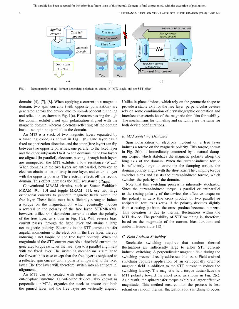
Fig. 1. Demonstration of (a) domain-dependent polarization effect, (b) MTJ stack, and (c) STT effect.
domains [4], [7], [8]. When applying a current to a magneticdomain, two spin currents (with opposite polarization) aregenerated across the device due to spin-dependent tunnelingand reflection, as shown in Fig. 1(a). Electrons passing throughthe domain exhibit a net spin polarization aligned with themagnetic domain, whereas electrons reflecting off the domainhave a net spin antiparallel to the domain.
An MTJ is a stack of two magnetic layers separated bya tunneling oxide, as shown in Fig. 1(b). One layer has afixed magnetization direction, and the other (free layer) can flipbetween two opposite polarities, one parallel to the fixed layerand the other antiparallel to it. When domains in the two layersare aligned (in parallel), electrons passing through both layersare unimpeded; the MTJ exhibits a low resistance (RLow).When domains in the two layers are antiparallel, however, anelectron obtains a net polarity in one layer, and enters a layerwith the opposite polarity. The electron reflects off the seconddomain. This effect increases the MTJ resistance (RHigh).
Conventional MRAM circuits, such as Stoner–WohlfarthMRAM [9], [10] and toggle MRAM [11], use two largeorthogonal currents to generate magnetic fields within thefree layer. These fields must be sufficiently strong to inducea torque on the magnetization, which eventually inducesa reversal in the polarity of the free layer. STT-MRAMs,however, utilize spin-dependent currents to alter the polarityof the free layer, as shown in Fig. 1(c). With reverse bias,current passes through the fixed layer and attains a largenet magnetic polarity. Electrons in the STT current transferangular momentum to the electrons in the free layer, therebyinducing a net torque on the free layer polarity. When themagnitude of the STT current exceeds a threshold current, thegenerated torque switches the free layer to a parallel alignmentwith the fixed layer. The switching mechanism is similar tothe forward bias case except that the free layer is subjected toa reflected spin current with a polarity antiparallel to the fixedlayer. The free layer will, therefore, switch into an antiparallelalignment.
An MTJ can be created with either an in-plane or anout-of-plane structure. Out-of-plane devices, also known asperpendicular MTJs, organize the stack to ensure that boththe pinned layer and the free layer are vertically aligned.
Unlike in-plane devices, which rely on the geometric shape toprovide a stable axis for the free layer, perpendicular devicesrely on some combination of crystallographic orientation andinterface characteristics of the magnetic thin film for stability.The mechanisms for tunneling and switching are the same forboth device configurations.
B. MTJ Switching Dynamics
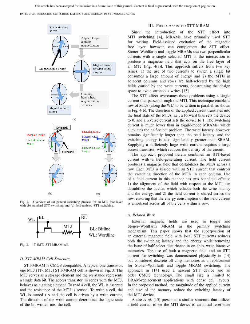
Spin polarization of electrons incident on a free layerinduces a torque on the magnetic polarity. This torque, shownin Fig. 2(b), is immediately countered by a natural damp-ing torque, which stabilizes the magnetic polarity along thelong axis of the domain. When the current-induced torqueis sufficiently large to overcome the damping torque, thedomain polarity aligns with the short axis. The damping torqueswitches sides and assists the current-induced torque, whichswitches the polarity of the domain.
Note that this switching process is inherently stochastic.Since the current-induced torque is parallel or antiparallelto the resting polarity of the device, the effective torque onthe polarity is zero (the cross product of two parallel orantiparallel torques is zero). If the polarity deviates slightlyfrom a resting position, the cross product becomes nonzero.This deviation is due to thermal fluctuations within theMTJ device. The probability of STT switching is, therefore,based on the magnitude of the current, bias duration, andambient temperature [12].
C. Field-Assisted Switching
Stochastic switching requires that random thermalfluctuations are sufficiently large to allow STT current-induced switching. A perpendicular magnetic field during theswitching process directly addresses this issue. Field-assistedswitching requires application of an orthogonally orientedmagnetic field in addition to the STT current to reduce theswitching latency. The magnetic field torque destabilizes theMTJ polarity toward the short axis, as shown in Fig. 2(c).As a result, the spin-transfer torque exhibits a larger effectivemagnitude. This method ensures that the process is lessreliant on random thermal fluctuations for switching to occur.
This article has been accepted for inclusion in a future issue of this journal. Content is final as presented, with the exception of pagination.
PATEL et al.: REDUCING SWITCHING LATENCY AND ENERGY IN STT-MRAM CACHES 3
Fig. 2. Overview of (a) general switching process for an MTJ free layerwith (b) standard STT switching and (c) field-assisted STT switching.
Fig. 3. 1T-1MTJ STT-MRAM cell.
D. STT-MRAM Cell Structure
STT-MRAM is CMOS compatible. A typical one transistor,one MTJ (1T-1MTJ) STT-MRAM cell is shown in Fig. 3. TheMTJ serves as a storage element and the resistance representsa single data bit. The access transistor, in series with the MTJ,behaves as a gating element. To read a cell, the WL is assertedand the resistance of the MTJ is sensed. To write a cell, theWL is turned ON and the cell is driven by a write current.The direction of the write current determines the logic stateof the bit written into the cell.
III. FIELD-ASSISTED STT-MRAM
Since the introduction of the STT effect intoMTJ switching [4], MRAMs have primarily used STTfor writing. Field-assisted excitation of the magneticfree layer, however, can complement the STT effect.Stoner–Wohlfarth and toggle MRAMs use two perpendicularcurrents with a single selected MTJ at the intersection toproduce a magnetic field that acts on the free layer ofan MTJ [Fig. 4(a)]. This approach suffers from two keyissues: 1) the use of two currents to switch a single bitconsumes a large amount of energy and 2) the MTJs inadjacent columns and rows are half-selected by the highfields caused by the write currents, constraining the designspace to avoid erroneous writes [13].
The STT effect overcomes these problems using a singlecurrent that passes through the MTJ. This technique enables arow of MTJs (along the WL) to be written in parallel, as shownin Fig. 4(b). The direction of the applied current translates intothe final state of the MTJs, i.e., a forward bias sets the deviceto 0, and a reverse current sets the device to 1. The switchingcurrent is much lower than in toggle-mode MRAMs, whichalleviates the half-select problem. The write latency, however,remains significantly longer than the read latency, and theswitching energy is also significantly greater than SRAM.Supplying a sufficiently large write current requires a largeaccess transistor, which reduces the density of the circuit.
The approach proposed herein combines an STT-basedcurrent with a field-generating current. The field currentproduces a magnetic field that destabilizes the MTJs across arow. Each MTJ is biased with an STT current that controlsthe switching direction of the MTJs in each column. Useof a field current in this manner has two beneficial effects:1) the alignment of the field with respect to the MTJ candestabilize the device, which reduces both the write latencyand the energy, and 2) the field current is shared across therow, ensuring that the energy consumption of the field currentis amortized across all of the cells within a row.
A. Related Work
External magnetic fields are used in toggle andStoner–Wohlfarth MRAM as the primary switchingmechanism. This paper shows that the superposition ofan external magnetic field with local STT currents reducesboth the switching latency and the energy while removingthe issue of half-select disturbance in on-chip, write intensivememories. The use of both a magnetic field and an STTcurrent for switching was demonstrated physically in [14]but considered discrete off-chip memories as a replacementfor Stoner–Wohlfarth and toggle MRAM switching. Theapproach in [14] used a nascent STT device and anolder CMOS technology. The small size is limited toDRAM-replacement applications with dense cell layouts.In the proposed method, the magnitude of the applied currentand size of the memory reduce the switching latency ofthe MTJ device.
Andre et al. [15] presented a similar structure that utilizesa field current to set the MTJ device to an initial reset state
This article has been accepted for inclusion in a future issue of this journal. Content is final as presented, with the exception of pagination.
4 IEEE TRANSACTIONS ON VERY LARGE SCALE INTEGRATION (VLSI) SYSTEMS
Fig. 4. Current biasing scheme for (a) Stoner–Wohlfarth and toggle MRAM, (b) STT-MRAM, and (c) proposed field-assisted STT-MRAM.
TABLE I
LLG SIMULATION PARAMETERS
(either RON or ROFF) prior to writing the device. This methodenables the unidirectional cells and diodes to select theindividual memory cells [15], which provide cell densityadvantages appropriate for DRAM-replacement memoryapplications. A reset process, however, requires theMTJ devices to undergo two switching events for everywrite, one to switch to a reset state (either RON or ROFF), anda second switching event to write the correct state for theremaining bits. This process doubles the write latency of anMRAM array. The approach presented in this paper requiresCMOS transistors for bipolar switching and utilizes magneticfields to enhance the dynamic behavior of the switchingprocess to reduce the energy of a write, while sharing the fieldcurrent to amortize the energy across multiple columns. Thedevice is not reset to a stable state but rather an additionaltorque is applied dynamically to enhance the switchingprocess, reducing the overall write latency and enabling usein latency critical applications.
Ding [16], Wang et al. [17], and Cao et al. [18]describe individual cell structures used for field-assistedMRAM switching. Each of these publications describestructures and topologies for individual field-assistedMRAM cells. The key difference between these publicationsand the work presented in this paper is the notion of sharingthe field current across multiple cells across the WL. Systemlevel sharing of the field current results in a significantreduction in energy.
IV. MODEL OF A FIELD-ASSISTED STT-MRAM CELL
An individual in-plane MTJ is modeled here using theclassical Landau–Lifshitz–Gilbert (LLG) macrospin modelwith thermal agitation based on a Langvin random field usingthe M3 simulator [19], with parameters listed in Table I.While the proposed field-assisted mechanism is applicableto both in-plane and perpendicular devices, only an in-planedevice is considered here because of the relative maturity of
TABLE II
MTJ PARAMETERS
the technology. The MTJ free-layer parameters are selectedto ensure that the thermal stability factor (�) provides a10-year retention of the device state (� = 40). The MTJparameters for the resistance and tunneling magnetoresistanceratio (TMR) (from ITRS 2011 [20]) are listed in Table II.The critical switching current of the MTJ is dependent on thegeometric and material properties of the free layer, permittingthe current to be determined from the free-layer geometry. Theresultant critical current is in agreement with the switchingcurrent targeted by the ITRS [20]. Read simulations assumea worst case variation of 30% for both RON and ROFF. Datafor statistical variation of the thermal barrier are unavailable.Cache entries, however, exhibit lifetimes on the order ofseconds. Higher thermal barriers may lengthen the switchingtime of an MTJ. The relatively high thermal barrier assumedin this paper is conservative.
The predictive technology model is used to characterize thecell access transistor [21]. A low threshold transistor is usedfor the selection device and is modeled with a 20% reductionin threshold voltage. The WL is bootstrapped to VDD + Vth.The cell transistor width provides a switching current 1.5 timesgreater than the critical switching current. This width isselected to ensure that the device operates in precessionalmode [12] while allowing the access transistor to be small.
Durlam et al. [10] present a toggle MRAM cell and memory.Measurements of the field observed by the free layer aredemonstrated at a distance of 0.3 μm for a 0.6-μm process.Linear scaling of this dimension to a 22-nm process is assumedfor the field line spacing to evaluate the field-assisted cell, asshown in Fig. 5. Simple linear scaling of this dimension isnot sufficient, as the MTJ dimensions are proportionally largerthan in Stoner–Wohlfarth and toggle MRAM. To compensate,the MTJ dimensions are scaled linearly and the thickness ofthe MTJ stack is assumed to occupy an additional 10 nm.This thickness is typical of many demonstrated STT-MTJstacks [22], [23].
This article has been accepted for inclusion in a future issue of this journal. Content is final as presented, with the exception of pagination.
PATEL et al.: REDUCING SWITCHING LATENCY AND ENERGY IN STT-MRAM CACHES 5
Fig. 5. Profile view of field-assisted STT-MRAM cell.
Fig. 6. Physical layout of field-assisted STT-MRAM cell.
The cell layout is based on 45-nm FreePDK design rulesand scaled to 22 nm, as shown in Fig. 6. A spectrum ofcell sizes is evaluated for performance. The base cell areais 55.5 F2. In a prior work, the area of a conventional1T-1MTJ cell is shown to be 49.9 F2 with the same technologyrules, indicating that the area overhead of the metal linesupporting the additional field current is small [24], [25].This cell has a relatively large cell density as compared withcommodity STT-MRAM (6 F2 [20]), since the layout rulesoriginate from a logic oriented process. A standalone memoryprocess with tighter design rules would provide greater density.
Three distinct physical configurations of a 1T-1MTJmemory cell are compared in Table III. The field-assisted
TABLE III
STT-MRAM CELL PARAMETERS
TABLE IV
MEMORY ARRAY PARAMETERS
STT-MRAM cell (Field-Assisted) is compared with aminimum-sized 1T-1MTJ cell capable of supplying the samenominal switching current (Minimum). The additional metalline devoted to the field current impedes contact sharing andconsumes additional area as compared with the minimum cell.The third memory cell (Isometric) has the same total areaas the field-assisted cell. Due to extra area consumed by thebit lines above the silicon substrate, the field-assisted cellcan use a slightly larger transistor than the minimum cellwithout affecting cell density, resulting in a slightly largerSTT switching current.
The magnetic field through a current loop can be estimatedby the Bio–Savart’s law [26]
B = μ0 Ifield
2πd. (1)
The current through the MTJ induces a spin torque on thefree layer, generating a magnetic field that adds linearly to themagnetic field generated by the field current. The magneticfield produced by the STT is assumed to be negligible fortwo reasons. First, the STT current is almost two orders ofmagnitude smaller than the field current, making the fieldgenerated by the STT current relatively small. Second, thefield current is applied to the MTJ before the STT currentis applied, ensuring that the free-layer magnetization is in anunstable state prior to application of the STT current. As aresult, the magnetic field of the STT current does not affectthe destabilization process.
The deterministic switching latency with increasing fieldcurrent in the absence of thermal noise is shown in Fig. 7. Thelatency decreases monotonically with increasing field current,indicating that the maximum available current improves circuitspeed. Thermal noise is, however, an important concern, asdiscussed in Section V-A.
V. MODEL OF STT-MRAM ARRAY
Optimizing the energy consumed by an MRAM array with afield-assisted write produces a tradeoff between the size of thearray and the current bias when minimizing the switching timeof an MTJ. The parasitic impedances of the array, extractedfrom the cell layout, are listed in Table IV [21].
This article has been accepted for inclusion in a future issue of this journal. Content is final as presented, with the exception of pagination.
6 IEEE TRANSACTIONS ON VERY LARGE SCALE INTEGRATION (VLSI) SYSTEMS
Fig. 7. Switching latency of a field-assisted MRAM cell. STT switchingcurrent is 59.1 μA.
The array is biased using a field current that traversesthe entire row. As the size of the row increases, the energyassociated with the field current is amortized across the entirerow. The energy associated with the field current is the sumof the dynamic energy to charge the line and the static currentto generate the magnetic field. Expression (2) quantifies thisdependence, where Rflcell and Cflcell describe, respectively, theper cell parasitic resistance and capacitance, N describes thenumber of cells in a row, Rdriver is the resistance of the drivetransistor that supplies the field current, VDD is the supplyvoltage, tswitching is the MTJ switching latency, and Ifield isthe generated field current of the line. The first term in (2)describes the dynamic energy required to charge a field line,while the second term quantifies the static energy consumedby the field current. The dynamic component of the energy is,therefore, a function of array width and the dc voltage on thebit line during a write
Efield = 1
2Cflcell N
(N Rflcell
N Rflcell + RdriverVDD
)2
+ VDD Ifieldtswitching. (2)
The energy of the static current is a function of the fieldcurrent, supply voltage, and switching time of the MTJ. Thestatic component is independent of array size as the supplyvoltage is constant and the voltage drop is across the peripheralwrite drivers and the array. The array field current is alsoconstrained by the resistance of the field line
Ifield RflCell N ≤ VDD. (3)
The energy to switch a single MTJ (Eswitch) is
Eswitch = ISTTVDDtswitching (4)
where ISTT is the spin-torque switching current. Eswitch is,therefore, only dependent on the switching time of the MTJ.The total energy per bit is
Etotal = Eswitch + Efield
N. (5)
The switching energy is shown in Fig. 8. For comparison,the minimum energy to switch an MTJ, as described by (4),
Fig. 8. Switching energy of a field-assisted MRAM cell.
for a nonfield-assisted STT-MRAM cell, is 0.3 pJ/bit. Theminimum switching energy of the field-assisted cell is0.054 pJ/bit with a corresponding switching latency of 618 ps.Due to the bit line resistance, longer rows support a maximumfield current at a specific supply voltage. A sufficiently highfield cannot be generated to reduce the switching latency ofthe MTJ, ensuring that the energy consumption is higher thanwith a shorter row. An optimum row length, therefore, existsthat minimizes the overall switching energy of an array duringa write. For the configuration shown in Fig. 8, the optimumrow length is 128 cells.
As shown by the figure, increasing the number of cells ina row produces a linear increase in energy consumed per bit.However, as the row length increases, the maximum currentbecomes bounded. For latency critical as well as energy criticalcircuits, the field currents should be maximized for a given rowlength, and a larger current should be used rather than a longerrow, except for small row lengths.
Large field currents, however, have classically beenassociated with the half-select problem as magnetic fieldsmay interact with MTJs in adjacent rows. The high ther-mal stability assumed in this paper, however, preventserrors in the cache. Under an applied field, the expression,�(Happ) = �(1 − Happ/Hk)
2, governs the thermal stabilityof an MTJ [27]. For a 10-ns applied pulse, the immediatelyadjacent rows exhibit a bit-error rate (BER) of ∼10−15.This BER is small as compared with the lifetime of datawithin a high-performance cache, and is sufficient for practicaloperation.
A. Effects of Stochastic Switching
As noted previously, STT switching is a stochasticoperation [5]. While deterministic information is sufficient todetermine a suitable design point, practical design methodsrequire that the stochastic nature of the switching process beconsidered.
The energy and latency of each of the physical memorycells are listed in Table V. Each cell type is evaluated for arow length of 128 bits with a 6.5-mA field current applied to
This article has been accepted for inclusion in a future issue of this journal. Content is final as presented, with the exception of pagination.
PATEL et al.: REDUCING SWITCHING LATENCY AND ENERGY IN STT-MRAM CACHES 7
TABLE V
ENERGY AND LATENCY OF STT-MRAM CELLS
the MRAM device. The field-assisted cell exhibitsa significant reduction in energy and latency as compared withthe minimum and isometric STT cells. As the field is applied,the switching latency decreases; the standard deviation,however, falls disproportionately. A minimum-sized STT cellexhibits a switching latency of 4.96 ns with a 30% standarddeviation. While the field-assisted cell exhibits a reducedmean write latency of 0.47 ns, the standard deviation ofswitching is 102% of the mean. Intuitively, with increasingapplied field, the effect of the damping torque diminishes andthe system becomes more unpredictable during switching.This effect causes greater variability in the switching latency.To compensate for this variability and to enhance circuitspeed, a 90% write success rate is targeted. Write backcircuits are used to ensure proper operation, as describedin Section VI.
For comparative purposes, a field-assisted cell with reducednonvolatility is also presented. Unlike the baseline cell, thiscell assumes a reduced thermal barrier for the MTJ, whichlowers the retention time of the MTJ to one day. This com-bination produces the shortest latency and the lowest energyconfiguration. The reduced thermal barrier also exhibits noadditional variability as compared with the baseline field-assisted cell. In subsequent analyses, however, the baseline cellis designed to ensure that a typical industrial 10 year retentiontime is maintained [6].
VI. CACHE EVALUATION
The development of L1 and L2 caches with a field-assistedSTT-MRAM is evaluated in this section. SRAM caches andcaches using conventional STT-MRAM (without thefield-assisted switching mechanism) are treated as a baselinefor comparative purposes.
Naive replacement of SRAM arrays and sensing circuitrywith STT-MRAM arrays degrades the performance in writecritical caches due to the long switching latency, producingan unfair comparison. The baseline STT-MRAM (Minimumand Isometric) caches, therefore, incorporate two state-of-the-art architectural techniques to improve the system performancewhile tolerating write latency. The caches are typically dividedinto multiple subbanks to increase the parallel throughput ofdata accesses and to amortize the cost of the peripheral logiccircuitry. Subbank buffering [28] adds an SRAM write bufferin front of each cache subbank [Fig. 9(a)], which locallybuffers on-going writes. When data is stored within a subbankbuffer, the H-Tree data bus, which is shared across all of thesubarrays, serve the next cache access while the long latencySTT-MRAM write is local within the subbank. Decouplingthe access circuitry and interface bus from the long latency
Fig. 9. Array organization for (a) baseline STT-MRAM and (b) field-assistedSTT-MRAM.
TABLE VI
CACHE AND MEMORY PARAMETERS
write significantly improves cache throughput. In addition,differential writes [29] is a technique commonly used to reducewrite energy. Before a write, the stored data are read andcompared with the to-be-written data. Only those STT-MRAMcells with different binary states actually switch.
Field-assisted STT-MRAM caches [Fig. 9(b)] also employsubbank buffering, but do not incorporate differential writessince all of the STT-MRAM cells in a row are affected bythe field. To guarantee a successful STT-MRAM switchingprocess, a checker read is issued after every write. Upon awrite failure, a retry write is issued.
A. Simulation Setup
The cycle accurate SESC simulator [30] has been modifiedto model a chip multithreaded processor with eight cores andfour threads per core operating at 4 GHz. The three config-urations for the memory subsystem are listed in Table VI.A field-assisted STT-MRAM cache, an isometric cell cache,and a baseline SRAM configuration are explored in this paper.Isometric and field-assisted cells are used in the L1 cacheto evaluate the performance impact of a field-assisted cache.In the L2 cache, where write latency is not a critical parameter,minimum-sized cells are used. Both of these configurations arenormalized to an SRAM baseline configuration. CACTI [31]and NVSim [32] are used to estimate the cache energy andaccess latencies. The cache capacities are the same for boththe STT-MRAM and the SRAM caches. The cache latencies
This article has been accepted for inclusion in a future issue of this journal. Content is final as presented, with the exception of pagination.
8 IEEE TRANSACTIONS ON VERY LARGE SCALE INTEGRATION (VLSI) SYSTEMS
TABLE VII
STT-MRAM CACHE PARAMETERS (CYCLE: 250 ps)
Fig. 10. System performance of STT-MRAM caches normalized to baselineSRAM caches for each cell type.
Fig. 11. Energy of STT-MRAM caches normalized to baseline SRAM cachesfor baseline and field-assisted cell types.
for these configurations are summarized in Table VII. For thebaseline STT-MRAM cache configuration, the isometric cellsare used for the L1 caches to minimize the MTJ switchinglatency, and minimum-sized STT-MRAM cells are used for L2to decrease the cache area and read latency. The field-assistedSTT-MRAM cache configuration uses the field-assisted cellsfor all of the caches within the hierarchy.
A wide range of parallel workloads have been simulatedfor each configuration. The benchmark suite includes ninesoftware applications, among which three programs arefrom SPEC OMP2001 [33] and six programs are fromSPLASH2 [34]. All workloads are executed in 32 threads onan eight core processor.
B. System Performance, Energy, and Area
The system performance and cache energy are shownin Figs. 10 and 11. All of the comparisons are normalized tothe performance of the SRAM caches with the same capacity.
The field-assisted STT-MRAM caches exhibit a slightperformance increase as compared with the SRAM caches(Fig. 10) since the STT-MRAM caches occupy less areawhile maintaining the same capacity, hence benefiting from ashorter wire delay. The baseline STT-MRAM caches exhibit an
Fig. 12. Power dissipation of STT-MRAM and SRAM caches.
overall decrease in performance as compared with the baselineSRAM caches due to the long write latency. Despite subbankbuffering, the reads can be blocked by writes when subbankconflicts occur.
For these applications, STT-MRAM-based caches requireless energy (Fig. 11). The field-assisted STT-MRAM cachesconsume slightly higher energy as compared with the baselineSTT-MRAM caches due to two reasons: 1) the field currentconsumes additional energy and 2) differential writes areapplied to the baseline STT-MRAM but not to the field-assisted STT-MRAM. In the application LU, however, thefield-assisted STT-MRAM caches consume less energy. Thisbehavior occurs because LU uses a greater number of bit flipsduring writes. As a result, differential writes have less of aneffect on the write energy as compared with other applicationsusing isometric or minimum STT-MRAM cells.
The power dissipated by the benchmarks circuits is shownin Fig. 12 for STT-MRAM and SRAM caches. For all of theSTT-MRAM caches, the leakage power is less than SRAM.The power dissipated by the read operations is also less dueto the smaller array area and shorter wires. For the baselineSTT-MRAM caches, the power dissipated during the writeoperations is comparable with the power dissipated during theSRAM writes because the MTJs consume greater switchingpower but the access time is smaller than the SRAM caches.The field-assisted STT-MRAM caches require higher writepower due to the additional field currents applied during eachwrite. The field-assisted STT-MRAM caches, however, providefaster write and shorter execution time; hence, the effect of thefield currents on the total energy is amortized across the row.
Both caches are compared with the standard SRAM cachefor multiple applications. While the baseline STT-MRAMcache exhibits a reduction in total energy of 61.4%, theperformance drops by 23.1% as compared with SRAM. Thefield-assisted STT-MRAM cache exhibits a 54.7% reductionin energy as compared with SRAM, 6.7% more energy thanthe baseline STT-MRAM cache. Despite this small increasein energy, the field-assisted cache completes execution 4.8%faster than SRAM, a 28% performance improvement ascompared with the baseline STT-MRAM cache.
The area and area efficiency (AE) of the field-assistedcaches, isometric caches, and SRAM baseline caches are listedin Table VIII. The AE of a cache describes the area of thememory cells as compared with the total area of the cache,
This article has been accepted for inclusion in a future issue of this journal. Content is final as presented, with the exception of pagination.
PATEL et al.: REDUCING SWITCHING LATENCY AND ENERGY IN STT-MRAM CACHES 9
TABLE VIII
AREA OF STT-MRAM CACHES
expressed as
AE = Cell area
Cache area× 100. (6)
The field-assisted and isometric cells exhibit similararea and AE. Notably, the AE drops significantly for MRAMmemories. The SRAM baseline cache achieves the samecapacity at a smaller area than either MRAM variant, sincethe overhead of the peripheral circuitry increases for MRAM.While the field-assisted cells require drive transistors for eachrow, the field-assisted cache exhibits less area for each subar-ray than the isometric cell cache due to the greater number ofsubbank buffers needed to manage the write latency. This areadifference, however, is small as compared with the total area ofthe L1 cache. The area of both STT cells requires marginallygreater area than an SRAM for a L1 cache. For the largerL2 cache, the density advantages of STT-MRAM are sufficientto reduce area. For the overall cache subsystem, bothSTT-MRAM configurations use 45.3% less area than anSRAM configuration due primarily to the significant areareduction of the L2 cache.
VII. CONCLUSION
A field-assisted approach is applied to MRAM cells toreduce the switching latency of an STT-MTJ. An array modelof the switching latency and energy consumption for differentfield currents and array sizes is described. It is shown thatthe per bit switching latency is reduced by a factor of 4.If nonvolatility constraints are relaxed, the overall switchinglatency is reduced by a factor greater than 10.
Several field-assisted STT-MRAM cells are compared withminimum-sized and isometric area-based STT-MRAM cells.Each of these cells is evaluated for a variety of applications andcompared with standard L1 and L2 SRAM cache. Thefield-assisted STT-MRAM cache demonstrates a 25% per-formance improvement as compared with a nonfield-assistedcache STT-MRAM cache and a 5% improvement as com-pared with an SRAM cache while reducing overall energyconsumption by an average of 55% as compared with anSRAM cache. The overall cache subsystem exhibits a 42.5%reduction in total area as compared with an SRAM variant,however, a 33% increase in the area of the L1 cache isobserved due to the additional peripheral circuitry required tointerface withS
¯TT-MRAM. The reduction in both switching
energy and latency support embedded high-performance
STT-MRAM-based cache subsystems, enabling the use ofSTT-MRAM in upper level caches within high-performancemicroprocessors.
REFERENCES
[1] L. Chang et al., “An 8T-SRAM for variability tolerance and low-voltageoperation in high-performance caches,” IEEE J. Solid-State Circuits,vol. 43, no. 4, pp. 956–963, Apr. 2008.
[2] W. Zhao, E. Belhaire, C. Chappert, and P. Mazoyer, “Spin transfertorque (STT)-MRAM–based runtime reconfiguration FPGA circuit,”ACM Trans. Embedded Comput. Syst., vol. 9, no. 2, pp. 1–16, Oct. 2009,Art. ID 14.
[3] S. Chung et al., “Fully integrated 54 nm STT-RAM with the smallestbit cell dimension for high density memory application,” in Proc. IEEEInt. Electron Devices Meeting, Dec. 2010, pp. 12.7.1–12.7.4.
[4] M. Hosomi et al., “A novel nonvolatile memory with spin torque transfermagnetization switching: Spin-RAM,” in IEEE Int. Electron DevicesMeeting, Tech. Dig., Dec. 2005, pp. 459–462.
[5] J. M. Slaughter et al., “High density ST-MRAM technology (Invited),”in Proc. IEEE Int. Electron Devices Meeting, Dec. 2012,pp. 29.3.1–29.3.4.
[6] C. W. Smullen, V. Mohan, A. Nigam, S. Gurumurthi, and M. R. Stan,“Relaxing non-volatility for fast and energy-efficient STT-RAM caches,”in Proc. IEEE 17th Int. Symp. High Perform. Comput. Archit., Feb. 2011,pp. 50–61.
[7] T. Kishi et al., “Lower-current and fast switching of a perpendicularTMR for high speed and high density spin-transfer-torque MRAM,” inProc. IEEE Int. Electron Devices Meeting, Dec. 2008, pp. 1–4.
[8] T. Kawahara et al., “2 Mb SPRAM (SPin-transfer torque RAM) withbit-by-bit bi-directional current write and parallelizing-direction currentread,” IEEE J. Solid-State Circuits, vol. 43, no. 1, pp. 109–120,Jan. 2008.
[9] S. S. P. Parkin et al., “Exchange-biased magnetic tunnel junctions andapplication to nonvolatile magnetic random access memory (invited),”J. Appl. Phys., vol. 85, no. 8, pp. 5828–5833, Apr. 1999.
[10] M. Durlam et al., “A low power 1 Mbit MRAM based on 1T1MTJ bitcell integrated with copper interconnects,” in IEEE Symp. VLSI CircuitsDig. Tech. Papers, Jun. 2002, pp. 158–161.
[11] B. N. Engel et. al, “A 4-Mb toggle MRAM based on a novel bit andswitching method,” IEEE Trans. Magn., vol. 41, no. 1, pp. 132–136,Jan. 2005.
[12] Z. Diao et al., “Spin-transfer torque switching in magnetic tunneljunctions and spin-transfer torque random access memory,” J. Phys.,Condens. Matter, vol. 19, no. 16, p. 165209, Apr. 2007.
[13] R. P. Robertazzi, D. C. Worledge, and J. Nowak, “Investigations of halfand full select disturb rates in a toggle magnetic random access memory,”Appl. Phys. Lett., vol. 92, no. 19, pp. 192510-1–192510-3, May 2008.
[14] W. C. Jeong, J. H. Park, J. H. Oh, G. T. Jeong, H. S. Jeong, and K. Kim,“Highly scalable MRAM using field assisted current induced switching,”in IEEE Symp. VLSI Technol. Dig. Tech. Papers, Jun. 2005, pp. 184–185.
[15] T. Andre, S. Tehrani, J. Slaughter, and N. Rizzo, “Structures andmethods for a field-reset spin-torque MRAM,” U.S. Patent 8 228 715,Jul. 24, 2012.
[16] Y. Ding, “Method and system for using a pulsed field to assistspin transfer induced switching of magnetic memory elements,”U.S. Patent 7 502 249, Mar. 10, 2009.
[17] X. Wang et al., “Magnetic field assisted STRAM cells,”U.S. Patent 8 400 825, Mar. 19, 2013.
This article has been accepted for inclusion in a future issue of this journal. Content is final as presented, with the exception of pagination.
10 IEEE TRANSACTIONS ON VERY LARGE SCALE INTEGRATION (VLSI) SYSTEMS
[18] X. Cao, H. Xi, W. Zhu, R. Lamberton, and K. Gao, “Field assistedswitching of a magnetic memory element,” U.S. Patent 8 422 277,Apr. 16, 2013.
[19] C. Mewes and T. Mewes. M3 Micromagnetic Simulator. [Online]. Avail-able: http://www.bama.ua.edu/~tmewes/Mcube/Mcube.shtml, accessedNov. 2013.
[20] The ITRS Technology Working Groups. International TechnologyRoadmap for Semiconductors (ITRS). [Online]. Available: http://public.itrs.net
[21] W. Zhao and Y. Cao, “New generation of predictive technology modelfor sub-45 nm early design exploration,” IEEE Trans. Electron Devices,vol. 53, no. 11, pp. 2816–2823, Nov. 2006.
[22] H. Zhao et. al, “Low writing energy and sub nanosecond spin torquetransfer switching of in-plane magnetic tunnel junction for spin torquetransfer random access memory,” J. Appl. Phys., vol. 109, no. 7,p. 07C720, Apr. 2011.
[23] S. Ikeda et. al, “A perpendicular-anisotropy CoFeB–MgO magnetictunnel junction,” Nature Mater., vol. 9, no. 9, pp. 721–724, Jul. 2010.
[24] R. Patel, E. Ipek, and E. Friedman, “STT-MRAM memory cells withenhanced on/off ratio,” in Proc. IEEE Int. Syst.-Chip Conf., Sep. 2012,pp. 148–152.
[25] R. Patel, E. Ipek, and E. G. Friedman, “2T–1R STT-MRAM memorycells for enhanced on/off current ratio,” Microelectron. J., vol. 45, no. 2,pp. 133–143, Feb. 2014.
[26] F. T. Ulaby, E. Michielssen, and U. Ravaioli, Fundamentals of AppliedElectromagnetics. Englewood Cliffs, NJ, USA: Prentice-Hall, 2010.
[27] D. D. Tang and Y.-J. Lee, Magnetic Memory: Fundamentals andTechnology. Cambridge, U.K.: Cambridge Univ. Press, 2010.
[28] X. Guo, E. Ipek, and T. Soyata, “Resistive computation: Avoidingthe power wall with low-leakage, STT-MRAM based computing,” inProc. IEEE/ACM Int. Symp. Comput. Archit., Jun. 2010, pp. 371–382.
[29] B. C. Lee, E. Ipek, O. Mutlu, and D. Burger, “Architecting phase changememory as a scalable dram alternative,” in Proc. IEEE/ACM Int. Symp.Comput. Archit., Jun. 2009, pp. 2–13.
[30] J. Renau et al. (Jan. 2005). SESC: SuperESCalar Simulator. Available:http://sesc.sourceforge.net
[31] N. Muralimanohar, R. Balasubramonian, and N. Jouppi, “OptimizingNUCA organizations and wiring alternatives for large cacheswith CACTI 6.0,” in Proc. 40th Annu. IEEE/ACM Int. Symp.Microarchitecture, Dec. 2007, pp. 3–14.
[32] X. Dong, C. Xu, Y. Xie, and N. P. Jouppi, “NVSim: A circuit-levelperformance, energy, and area model for emerging nonvolatile memory,”IEEE Trans. Comput.-Aided Design Integr. Circuits Syst., vol. 31, no. 7,pp. 994–1007, Jul. 2012.
[34] S. C. Woo, M. Ohara, E. Torrie, J. P. Singh, and A. Gupta,“The SPLASH-2 programs: Characterization and methodological con-siderations,” in Proc. IEEE/ACM Int. Symp. Comput. Archit., Jun. 1995,pp. 24–36.
Ravi Patel (S’09) received the B.Sc. andM.Sc. degrees in electrical and computer engineeringfrom the University of Rochester, Rochester, NY,USA, in 2008 and 2010, respectively, where he iscurrently pursuing the Ph.D. degree.
He was a Research Intern with FreescaleSemiconductor Inc., Tempe, AZ, USA, in 2010and 2012, and imec, Leuven, Belgium, in 2014,where he was investigating power network designsub-10-nm integrated circuits. His current researchinterests include memristors, STT-MRAM, and high
performance memories.
Xiaochen Guo (S’09) received the master’s degreein electrical and computer engineering from theUniversity of Rochester, Rochester, NY, USA, andthe bachelor’s degree in computer science and engi-neering from Beihang University, Beijing, China.She is currently pursuing the Ph.D. degree with theUniversity of Rochester.
Dr. Guo was a twice recipient of the IBMPh.D. Fellowship.
Qing Guo (S’15) received the B.E. degree inautomation from Xi’an Jiaotong University, Xi’an,China, in 2007, and the M.S. degree in computerscience from the University of Rochester, Rochester,NY, USA, in 2012, where he is currently pursuingthe Ph.D. degree in computer science.
His current research interests include broad areaof computer architecture, with an emphasis onenergy efficient computing and architectures exploit-ing resistive memory technologies.
Engin Ipek (M’09) received the B.S., M.S., andPh.D. degrees from Cornell University, Ithaca, NY,USA, in 2003, 2007, and 2008, respectively, all inelectrical and computer engineering.
He was a Researcher with the Computer Archi-tecture Group with Microsoft Research, Redmond,WA, USA, from 2007 to 2009. He is currently anAssistant Professor of Electrical and ComputerEngineering and Computer Science with theUniversity of Rochester, Rochester, NY, USA, wherehe leads the Computer Systems Architecture
Laboratory. His current research interests include energy-efficient architec-tures, high performance memory systems, and the application of emergingmemory technologies to computer systems.
Dr. Ipek’s research has been recognized by the IEEE Computer SocietyTCCA Young Computer Architect Award in 2014, two IEEE Micro Top PicksAwards, an Invited Communications of the ACM Research Highlights Article,the ASPLOS 2010 Best Paper Award, and the NSF CAREER Award.
Eby G. Friedman (F’00) received the B.S. degreefrom Lafayette College, Easton, PA, USA, in 1979,and the M.S. and Ph.D. degrees from the Universityof California at Irvine, Irvine, CA, USA, in 1981and 1989, respectively, all in electrical engineering.
He was with Hughes Aircraft Company, from1979 to 1991, where he became the Manager ofthe Signal Processing Design and Test Departmentand was responsible for the design and test of highperformance digital and analog ICs. He has beenwith the Department of Electrical and Computer
Engineering, University of Rochester, Rochester, NY, USA, since 1991,where he is currently a Distinguished Professor, and the Director of theHigh Performance VLSI/IC Design and Analysis Laboratory. He is also aVisiting Professor with the Technion—Israel Institute of Technology, Haifa,Israel. He has authored over 400 papers and book chapters, holds 12 patents,and has authored and edited about 16 books in high-speed and low-powerCMOS design techniques, 3-D design methodologies, high-speed interconnect,and the theory and application of synchronous clock and power distributionnetworks. His current research interests include high performance synchronousdigital and mixed-signal microelectronic design and analysis with applicationto high-speed portable processors and low-power wireless communications.
Dr. Friedman is a Senior Fulbright Fellow. He was a recipient of the IEEECircuits and Systems 2013 Charles A. Desoer Technical Achievement Award,the University of Rochester Graduate Teaching Award, and the College ofEngineering Teaching Excellence Award. He was the Editor-in-Chief andChair of the Steering Committee of the IEEE TRANSACTIONS ON VERY
LARGE SCALE INTEGRATION SYSTEMS, the Regional Editor of the Journalof Circuits, Systems and Computers, a member of the Editorial Board of theIEEE PROCEEDINGS, the IEEE TRANSACTIONS ON CIRCUITS AND
SYSTEMS II: ANALOG AND DIGITAL SIGNAL PROCESSING, the IEEEJOURNAL ON EMERGING AND SELECTED TOPICS IN CIRCUITS AND
SYSTEMS, and the Journal of Signal Processing Systems, a member of theCircuits and Systems Society Board of Governors, and the Program andTechnical Chair of several IEEE conferences. He is also the Editor-in-Chiefof the Microelectronics Journal, a member of the Editorial Boards of theAnalog Integrated Circuits and Signal Processing, the Journal of Low PowerElectronics, and the Journal of Low Power Electronics and Applications, anda member of the Technical Program Committee of numerous conferences.