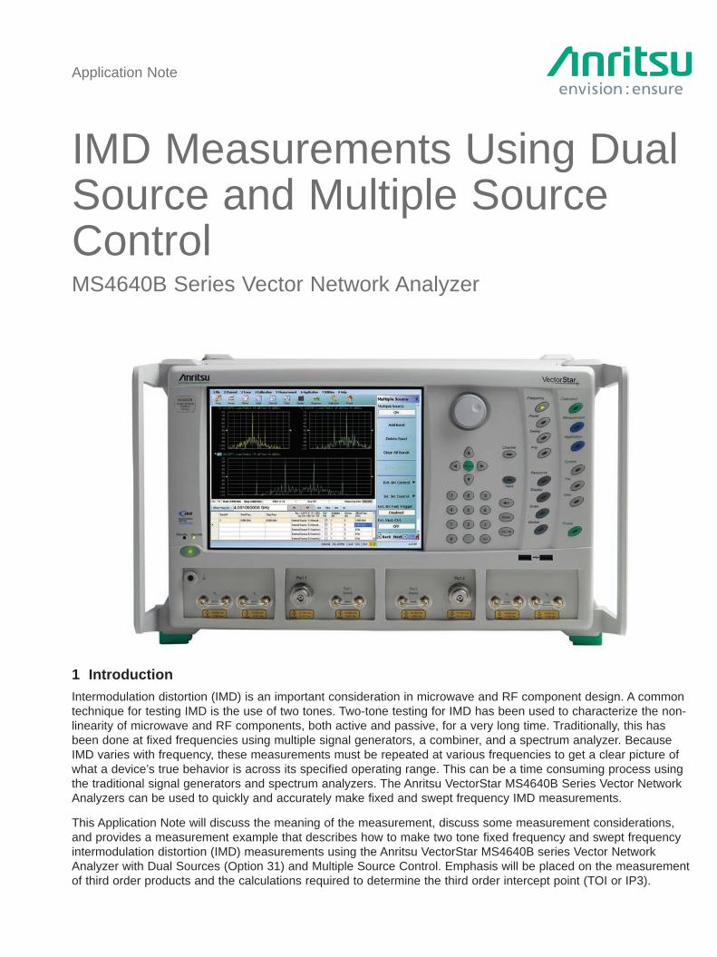
Application Note 1 Introduction Intermodulation distortion (IMD) is an important consideration in microwave and RF component design. A common technique for testing IMD is the use of two tones. Two-tone testing for IMD has been used to characterize the non- linearity of microwave and RF components, both active and passive, for a very long time. Traditionally, this has been done at fixed frequencies using multiple signal generators, a combiner, and a spectrum analyzer. Because IMD varies with frequency, these measurements must be repeated at various frequencies to get a clear picture of what a device’s true behavior is across its specified operating range. This can be a time consuming process using the traditional signal generators and spectrum analyzers. The Anritsu VectorStar MS4640B Series Vector Network Analyzers can be used to quickly and accurately make fixed and swept frequency IMD measurements. This Application Note will discuss the meaning of the measurement, discuss some measurement considerations, and provides a measurement example that describes how to make two tone fixed frequency and swept frequency intermodulation distortion (IMD) measurements using the Anritsu VectorStar MS4640B series Vector Network Analyzer with Dual Sources (Option 31) and Multiple Source Control. Emphasis will be placed on the measurement of third order products and the calculations required to determine the third order intercept point (TOI or IP3). IMD Measurements Using Dual Source and Multiple Source Control MS4640B Series Vector Network Analyzer
Transcript
Application Note
1 Introduction
Intermodulation distortion (IMD) is an important consideration in microwave and RF component design. A common technique for testing IMD is the use of two tones. Two-tone testing for IMD has been used to characterize the non-linearity of microwave and RF components, both active and passive, for a very long time. Traditionally, this has been done at fixed frequencies using multiple signal generators, a combiner, and a spectrum analyzer. Because IMD varies with frequency, these measurements must be repeated at various frequencies to get a clear picture of what a device’s true behavior is across its specified operating range. This can be a time consuming process using the traditional signal generators and spectrum analyzers. The Anritsu VectorStar MS4640B Series Vector Network Analyzers can be used to quickly and accurately make fixed and swept frequency IMD measurements.
This Application Note will discuss the meaning of the measurement, discuss some measurement considerations, and provides a measurement example that describes how to make two tone fixed frequency and swept frequency intermodulation distortion (IMD) measurements using the Anritsu VectorStar MS4640B series Vector Network Analyzer with Dual Sources (Option 31) and Multiple Source Control. Emphasis will be placed on the measurement of third order products and the calculations required to determine the third order intercept point (TOI or IP3).
IMD Measurements Using Dual Source and Multiple Source ControlMS4640B Series Vector Network Analyzer
2
2 What is Intermodulation Distortion (IMD)
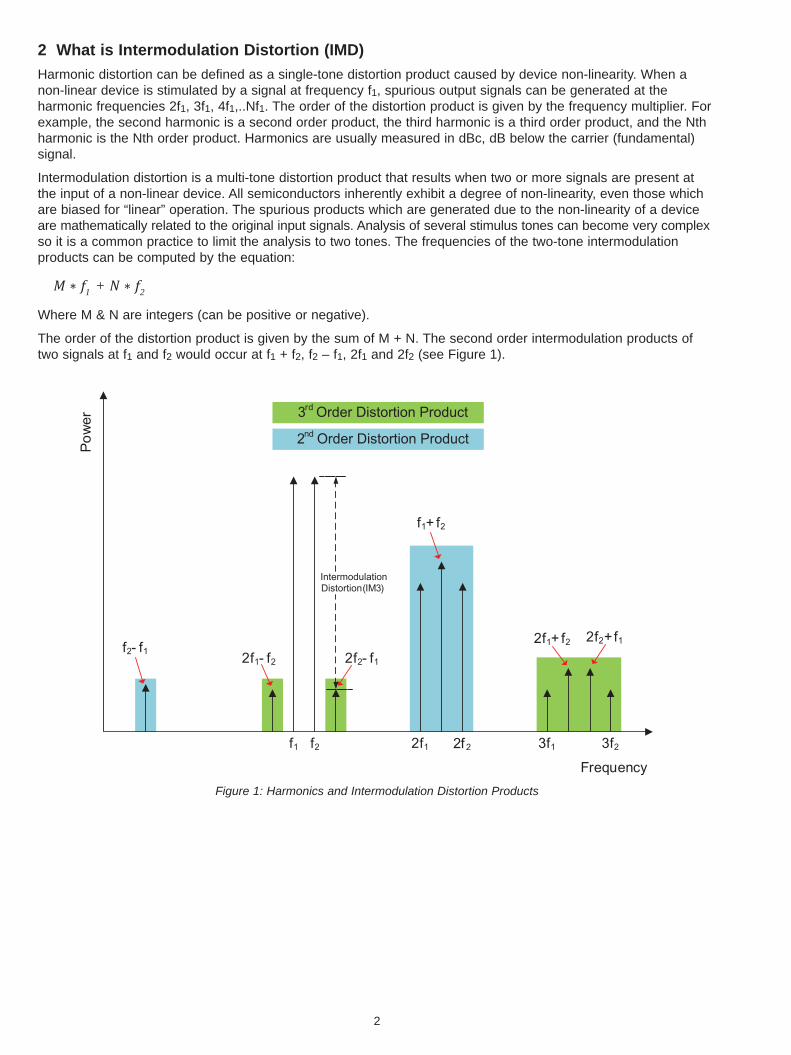
Harmonic distortion can be defined as a single-tone distortion product caused by device non-linearity. When a non-linear device is stimulated by a signal at frequency f1, spurious output signals can be generated at the harmonic frequencies 2f1, 3f1, 4f1,..Nf1. The order of the distortion product is given by the frequency multiplier. For example, the second harmonic is a second order product, the third harmonic is a third order product, and the Nth harmonic is the Nth order product. Harmonics are usually measured in dBc, dB below the carrier (fundamental) signal.
Intermodulation distortion is a multi-tone distortion product that results when two or more signals are present at the input of a non-linear device. All semiconductors inherently exhibit a degree of non-linearity, even those which are biased for “linear” operation. The spurious products which are generated due to the non-linearity of a device are mathematically related to the original input signals. Analysis of several stimulus tones can become very complex so it is a common practice to limit the analysis to two tones. The frequencies of the two-tone intermodulation products can be computed by the equation:
Where M & N are integers (can be positive or negative).
The order of the distortion product is given by the sum of M + N. The second order intermodulation products of two signals at f1 and f2 would occur at f1 + f2, f2 – f1, 2f1 and 2f2 (see Figure 1).
Figure 1: Harmonics and Intermodulation Distortion Products
f1 f2 2f1 2f2 3f1 3f2
3rd Order Distortion Product
2nd Order Distortion Product
f1+ f2
2f1+ f2
2f1- f2 2f2- f1
2f2+ f1
Frequency
Po
we
r
IntermodulationDistortion (IM3)
f2- f1
∗ 1 + ∗ 2
2f1 + f2 + f1 1, 2f1 – f2, 2f2 , and f
3rd order intermodulation product
–2f2
3 = + | 32
|
3 = +10 + |
|
( 20 – [−40 ]) 2 |
|
= +10 + 60
2
= +40
IP3 (dBm ) = P
P
OIP3P P
(dBm ) + IM3(dB)
2
3 = 0 + |
|
(10 – [−
−
70 ]) 2 |
|
3 = =
0 + |(+10 – [−70 ])
2|
= 0 + 80
2
= +40
= 3
+ | 32 | + | 3
2 | and
3
Third order intermodulation products of the two signals, f1 and f2, would be:
Where 2f1 is the second harmonic of f1 and 2f2 is the second harmonic of f2.
Mathematically the f2 – 2f1 and f1 – 2f2 intermodulation product calculations could result in a “negative” frequency. However, it is the absolute value of these calculations that is of concern. The absolute value of f1 – 2f2 is the same as the absolute value of 2f2 – f1. It is common to talk about the third order intermodulation products as being 2f1 ± f2 and 2f2 ± f1. Two of the most challenging distortion products are the signal content due to third-order distortion that occurs directly adjacent to the two input tones at 2f1 – f2 and 2f2 – f1. IMD measurement, then, describes the power ratio between the power level of the output fundamental tones (f2 and f1) and the third-order distortion products (2f1 – f2 and 2f2 – f1).
Broadband systems may be affected by all the non-linear distortion products. Narrowband circuits are only susceptible to those in the passband. Bandpass filtering can be an effective way to eliminate most of the undesired products without affecting inband performance. However, third order intermodulation products are usually too close to the fundamental signals to be filtered out. For example, if the two signals are separated by 1 MHz, then the third order intermodulation products will be 1 MHz on either side of the two fundamental signals. The closer the fundamental signals are to each other the closer these products will be to them. Filtering becomes impossible if the intermodulation products fall inside the passband. As a practical example, when strong signals from more than one transmitter are present at the input to the receiver, as is commonly the case in cellular telephone systems, IMD products will be generated. The level of these undesired products is a function of the power received and the linearity of the receiver/preamplifier.
3 Third-Order Intercept
As discussed earlier, spurious output signals can be generated at the harmonic frequencies of the fundamental signals, and the order of the distortion products is given by the frequency multiplier. The third order products are of particular interest for designers of RF and microwave systems as these products are usually too close to the fundamental signals to be filtered out. Therefore, it is important to measure and characterize these distortion products.
Fundamentally, IMD describes the ratio between the power of fundamental tones and the Nth order distortion products. For our discussion, we will focus on the 3rd order IMD ratio, commonly call IM3. It is important to understand that the IM3 ratio greatly depends on the power levels of the fundamental tones. As one continues to increase the power level of a two-tone stimulus, the IM3 ratio will decrease as a function of input power. At some arbitrarily high input power level, the 3rd order distortion products would theoretically be equal in power to the fundamental tones (for amplifiers, it is important to understand that this is an unrealistic condition since most amplifiers will saturate long before the intercept point is reached). This theoretical power level at which the fundamental and third-order products are equal in power is called the third-order intercept (TOI) and is also called IP3.
∗ 1 + ∗ 2
2f1 + f2 + f1 1, 2f1 – f2, 2f2 , and f
3rd order intermodulation product
–2f2
3 = + | 32
|
3 = +10 + |
|
( 20 – [−40 ]) 2 |
|
= +10 + 60
2
= +40
IP3 (dBm ) = P
P
OIP3P P
(dBm ) + IM3(dB)
2
3 = 0 + |
|
(10 – [−
−
70 ]) 2 |
|
3 = =
0 + |(+10 – [−70 ])
2|
= 0 + 80
2
= +40
= 3
+ | 32 | + | 3
2 | and
4
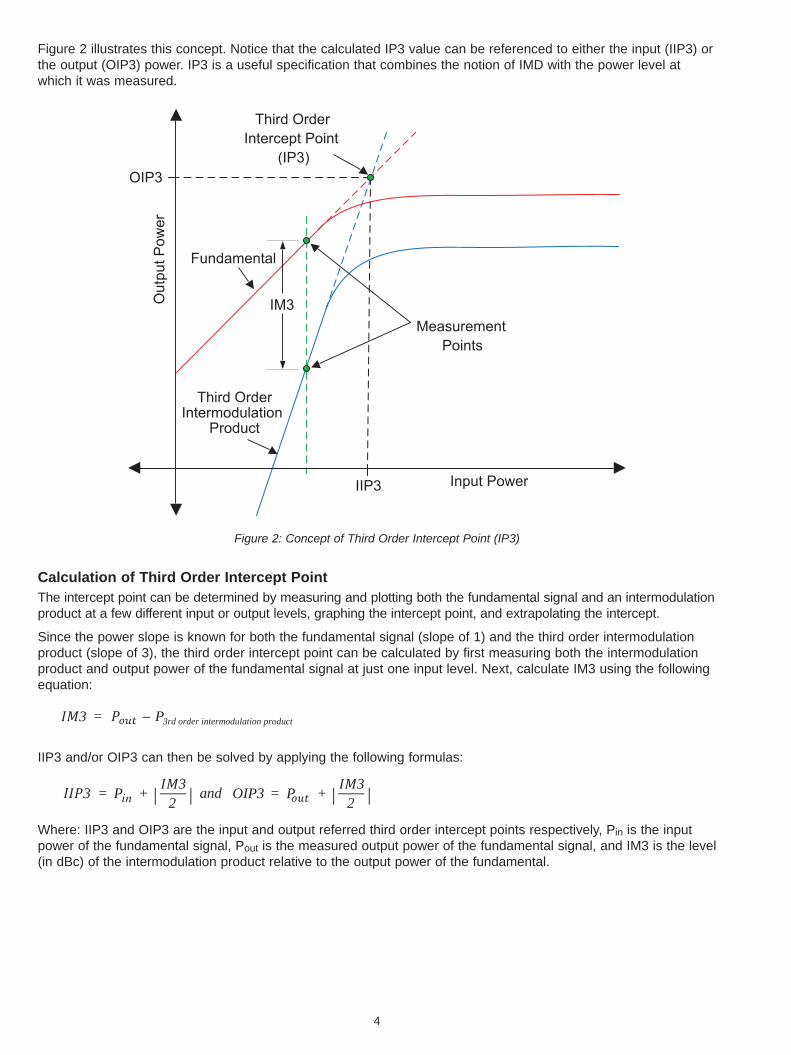
Calculation of Third Order Intercept PointThe intercept point can be determined by measuring and plotting both the fundamental signal and an intermodulation product at a few different input or output levels, graphing the intercept point, and extrapolating the intercept.
Since the power slope is known for both the fundamental signal (slope of 1) and the third order intermodulation product (slope of 3), the third order intercept point can be calculated by first measuring both the intermodulation product and output power of the fundamental signal at just one input level. Next, calculate IM3 using the following equation:
IIP3 and/or OIP3 can then be solved by applying the following formulas:
Where: IIP3 and OIP3 are the input and output referred third order intercept points respectively, Pin is the input power of the fundamental signal, Pout is the measured output power of the fundamental signal, and IM3 is the level (in dBc) of the intermodulation product relative to the output power of the fundamental.
Figure 2: Concept of Third Order Intercept Point (IP3)
Third Order Intermodulation
Product
Input Power
Out
put P
ower
Fundamental
Third Order Intercept Point
(IP3)OIP3
IIP3
Measurement Points
IM3
∗ 1 + ∗ 2
2f1 + f2 + f1 1, 2f1 – f2, 2f2 , and f
3rd order intermodulation product
–2f2
3 = + | 32
|
3 = +10 + |
|
( 20 – [−40 ]) 2 |
|
= +10 + 60
2
= +40
IP3 (dBm ) = P
P
OIP3P P
(dBm ) + IM3(dB)
2
3 = 0 + |
|
(10 – [−
−
70 ]) 2 |
|
3 = =
0 + |(+10 – [−70 ])
2|
= 0 + 80
2
= +40
= 3
+ | 32 | + | 3
2 | and
Figure 2 illustrates this concept. Notice that the calculated IP3 value can be referenced to either the input (IIP3) or the output (OIP3) power. IP3 is a useful specification that combines the notion of IMD with the power level at which it was measured.
∗ 1 + ∗ 2
2f1 + f2 + f1 1, 2f1 – f2, 2f2 , and f
3rd order intermodulation product
–2f2
3 = + | 32
|
3 = +10 + |
|
( 20 – [−40 ]) 2 |
|
= +10 + 60
2
= +40
IP3 (dBm ) = P
P
OIP3P P
(dBm ) + IM3(dB)
2
3 = 0 + |
|
(10 – [−
−
70 ]) 2 |
|
3 = =
0 + |(+10 – [−70 ])
2|
= 0 + 80
2
= +40
= 3
+ | 32 | + | 3
2 | and
5
For example, if a device is driven by two signals, f1 and f2, at an input power of +10 dBm each, with a resulting 10 dB gain of the main tones and 3rd order intermodulation products of –40 dBm, then the calculated value for IIP3 would be +40 dBm:
While it is important to take data with the device operating in the linear region, from the standpoint of practical intermodulation distortion measurements, the products should be as high above the noise floor of the measuring device as possible. This can be achieved by setting the power of the main tones as high as possible without compressing the DUT. Using the previous example, if the input power is dropped 10 dB to 0 dBm, the third order intermodulation products will drop by 30 dB to –70 dBm.
While the calculation still yields +40 dBm for the third order intercept point, making an accurate measurement of a signal at –70 dBm may be much more difficult and slower than one at –40 dBm.
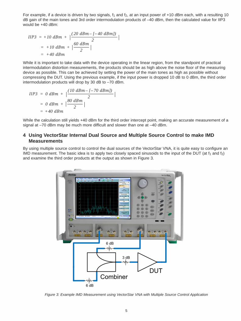
4 Using VectorStar Internal Dual Source and Multiple Source Control to make IMD Measurements
By using multiple source control to control the dual sources of the VectorStar VNA, it is quite easy to configure an IMD measurement. The basic idea is to apply two closely spaced sinusoids to the input of the DUT (at f1 and f2) and examine the third order products at the output as shown in Figure 3.
DUTCombiner
3 dB
6 dB
6 dB
6 dB
Figure 3: Example IMD Measurement using VectorStar VNA with Multiple Source Control Application
∗ 1 + ∗ 2
2f1 + f2 + f1 1, 2f1 – f2, 2f2 , and f
3rd order intermodulation product
–2f2
3 = + | 32
|
3 = +10 + |
|
( 20 – [−40 ]) 2 |
|
= +10 + 60
2
= +40
IP3 (dBm ) = P
P
OIP3P P
(dBm ) + IM3(dB)
2
3 = 0 + |
|
(10 – [−
−
70 ]) 2 |
|
3 = =
0 + |(+10 – [−70 ])
2|
= 0 + 80
2
= +40
= 3
+ | 32 | + | 3
2 | and
6
Typically b2/1 is the response variable and the measurement can be constructed to be CW to look like a spectrum analyzer output (as shown in Figure 4), or swept to reveal the IMD product magnitude vs. frequency in either dBc or dBm terms (as shown in Figure 5).
Figure 4: CW IMD Measurement Example
Figure 5: Swept Frequency IMD Measurement Example
7
4.1 Measurement Considerations
There are a number of things to consider when making intermodulation product measurements. This section will present some of the most common things to be aware of.
Combiner IsolationIsolation between the two input ports of the combiner is important. To understand why this is the case, one must understand how the VectorStar’s internal Automatic Level Control (ALC) treats unwanted signals. The presence of a signal from one source port at the output of the second source port will cause its output level to modulate (this is not specific to the VectorStar, as it is common to most signal generators). When the unwanted signal is detected by the VectorStar’s ALC, the VectorStar will try to remove the unwanted signal by generating AM onto the desired signal, thus canceling the modulation caused by the foreign signal. This results in the VectorStar no longer producing a single signal at the required frequency, but also producing side bands (beat notes) at an offset from this signal. This offset is equal to the difference between the desired and unwanted signals which makes them indistinguishable from intermodulation products that may be generated by the device under test. In general, 20 dB of isolation is recommended if one is to measure IMD products in the –80 to –90 dBc range.
DUT ConsiderationsInput power level requirements can be quite different depending on the type of device being tested and the test specifications. Some devices need to be tested at or near compression and others must be tested below the compression point. Thus, the optimal input drive level for a particular DUT must be chosen with care. In our example, we are using a wideband amplifier with the compression point being different at differing frequencies. Care must be taken when selecting the proper power level of the input tones such that when they are swept in frequency, the DUT is still driven at the desired test levels.
Signal Source Considerations1
Power:As stated above, different DUTs have differing drive level requirements. The VectorStar Series VNAs have a wide available power range to meet the demands of a large variety of devices. The maximum drive level of the VectorStar depends on the frequency at which it is operating.
Harmonics:Source harmonic performance, specifically the second harmonic, must be taken into account when making IMD measurements, especially two-tone third-order measurements (which is what we are doing). To understand the reason for this, remember that we are mainly interested in the 3rd order intermodulation products, 2f1 – f2 & 2f2 – f1. If source one is used to generate f1, it will also generate a second harmonic at 2f1. The unintended harmonic generated by source one at 2f1 will mix with the intended signal generated at f2 by generator two, producing a signal at the same frequency as the 3rd order intermodulation distortion signal (2f1 – f2) from the DUT. The same thing will happen with the second harmonic of source two, generating a signal at 2f2 – f1. In other words, the third-order distortion signals generated by the DUT from the two intended incident tones (f1 & f2) occurs at the same frequencies (2f1 – f2, 2f2 – f1) as those produced as a result of mixing one tone and the second harmonic of the other tone. Therefore if the second harmonics of the sources are incident upon the DUT, the DUT will generate signals at the intermodulation frequencies that will add to the signals we are trying to measure, thus causing errors in the measurements. The magnitude of this error depends upon the levels of the incident harmonic signals and the efficiency of the mixing process in the DUT.
Spurious Signals:All signal generators generate low-level spurious signals at some frequencies. These spurs can cause errors in IMD measurements if the spurious responses occur at or near the intermodulation frequencies being measured.
1 Consult the VectorStar MS4640B Series Technical Data Sheet (Anritsu Document # 11410-00611) for detailed Signal Source specifications.
8
Receiver Considerations2
Receiver Linearity:If the receiver generates its own IMD products, these will convolve with the products generated by the DUT and make results difficult to interpret.
Dynamic Range & Noise Floor:Dynamic range is the ratio between the largest and smallest possible signals that can be measured within a given receiver band. This is important if your 3rd order IM products are very low level signals. At mm-wave frequencies, this becomes a major issue since the noise floor of traditional mm-wave modules can be high. The non-linear shockline technology of the VectorStar Broadband system improves noise floor performance to significantly improve mm-wave IMD measurements.
The specified noise floor of the VNA will dictate the absolute minimum power level of the intermodulation signals it is able to measure. The typical noise floor of the VectorStar VNA at the b2 loop is about –120 dBm from 10 MHz to 70 GHz at 10 Hz IF BW.
Low-Level and High Level Random Noise:Random noise occurs both as low-level noise, which is independent of the signal power, and high-level noise, which is relative to the signal power. Both low and high level noise can contribute to measurement uncertainties.
Receiver Compression:Care must be taken to avoid overdriving the VNA’s receiver. For this example measurement, we are taking the measurement directly at the b2 loop. The VectorStar’s 0.1 dB receiver compression level is typically –5 to –1 dBm at the b2 port for most frequencies.
Mixing Products (Images):VNAs typically will not have Image rejection filters. Care must be taken to ensure the IMD products are not at the same frequencies as the images of the input signals.
Power Accuracy:This has two different aspects:
1. Often the DUT IMD products will be extremely power sensitive so an inaccurate drive level will put the DUT into an unintended state
2. Some expressions of intermodulation distortion have absolute power dependencies (intercept point and IMD (dBm) among them) so power inaccuracies will translate directly to the result. The latter effect happens in part since the drive power accuracy is coupled to the receiver calibration. A tertiary effect can occur with these calibrations if interpolation is invoked by changing the frequency list after calibration; these interpolation effects are most severe for highly mismatched test structures and a low density of calibration points.
Mismatch:Aside from simple issues of how much power is actually delivered to the DUT (reduced by mismatch at the input plane) and inaccuracies induced in the receiver calibration (from mismatch between source and receiver), there can be issues of different mismatch levels at a product frequency versus that at a main tone frequency. This is mainly an issue for large tone deltas and longer electrical length setups (which follows from this situation allowing a major standing wave change on the scale of a tone delta). A well-matched combiner and receiver structure can help with this effect. There are a number of different dependencies that may be of interest in the IMD class. Obvious ones include bias and tone power. Since this is usually a quasi-linear measurement, these dependencies will often be far more severe than for S-parameter measurements. Another obvious dependency is that with frequency (of the main tone average). Less obvious perhaps is the dependence on the separation between tones. Some interesting behaviors can be seen where the tone difference frequency can excite bias thermal and trapping behaviors causing an intermodulation response at other orders. These effects often show up in intermodulation product asymmetry.
4.2 Calibration Considerations
When performing any VNA measurement, proper calibrations must be performed in order to get accurate measurements. For IMD measurements, a full 12-term 2-port calibration is neither required nor possible. This is because the intermodulation products that we are measuring are at different frequencies than the fundamental signals. However, we will have to do power and receiver calibrations as the IMD measurements rely on absolute power measurements.
2 Consult the VectorStar MS4640B Series Technical Data Sheet (Anritsu Document # 11410-00611) for detailed Receiver specifications.
9
4.3 Measurement Example
For this example measurement the following equipment will be used:
• Anritsu MS4647B VectorStar VNA with Dual Source Option 31
• Anritsu ML2496A Power Meter
• Anritsu MA2474A Power Sensor
• Microwave Communication Laboratories PS2-196, 0.4 to 18 GHz combiner
We will be using the dual sources (option 31) of the VectorStar VNA to generate the two tones. Ports 1 & 2 of the VNA will be the source ports and the b2 receiver will be connected directly to the output of the DUT via the b2 loop as shown in Figure 3. Please note that for this configuration, we will be connecting directly to the b2 loop on the front panel, thereby setting up a measurement for 2.5 GHz and above in a single sweep. If measurements must be made below 2.5 GHz, a diplexer may be used.
Initialize VectorStar1) Preset Instrument to ensure it is in a known state
2) Set Frequency Range and number of points for the measurement. Note that the Start and Stop Frequencies must be chosen with care to account for the frequency offsets of the fundamental tones and 3rd order harmonic products. Also note that for the best accuracy, the number of points chosen should result in frequency steps that fall on the fundamental and harmonic frequencies.
a) Start: = 9.995 GHz
b) Stop = 12.01 GHz
c) # of Points = 404
d) CW Mode = OFF
3) Set IF BW to 1 kHz.
a) Channel → Averaging → IFBW = 1 kHz
Setup DisplayNext, we will setup the display to show the result. As discussed above, this is an absolute measurement using the b2 receiver. Therefore, we shall setup the response to be b2/1.
1) Trace → # of Traces = 1 → Trace Layout (select single layout as shown)
2) Setup Trace Format to display Log Magnitude
a. Display → Trace Format → Log Mag
3) Set the Response as follows: Response → User-defined →
a. Numerator = b2, Denominator = 1, Driver Port = Port 1
10
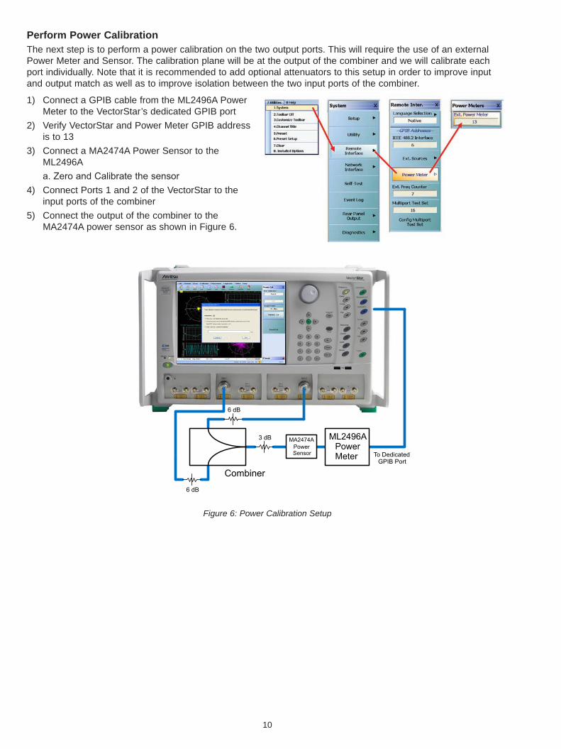
Perform Power CalibrationThe next step is to perform a power calibration on the two output ports. This will require the use of an external Power Meter and Sensor. The calibration plane will be at the output of the combiner and we will calibrate each port individually. Note that it is recommended to add optional attenuators to this setup in order to improve input and output match as well as to improve isolation between the two input ports of the combiner.
1) Connect a GPIB cable from the ML2496A Power Meter to the VectorStar’s dedicated GPIB port
2) Verify VectorStar and Power Meter GPIB address is to 13
3) Connect a MA2474A Power Sensor to the ML2496A
a. Zero and Calibrate the sensor
4) Connect Ports 1 and 2 of the VectorStar to the input ports of the combiner
5) Connect the output of the combiner to the MA2474A power sensor as shown in Figure 6.
Combiner
MA2474APower Sensor
ML2496APowerMeter To Dedicated
GPIB Port
6 dB
6 dB
3 dB
Figure 6: Power Calibration Setup
11
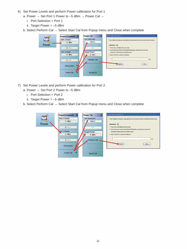
6) Set Power Levels and perform Power calibration for Port 1
a. Power → Set Port 1 Power to –5 dBm → Power Cal →
i. Port Selection = Port 1
ii. Target Power = –5 dBm
b. Select Perform Cal → Select Start Cal from Popup menu and Close when complete
7) Set Power Levels and perform Power calibration for Port 2
a. Power → Set Port 2 Power to –5 dBm
i. Port Selection = Port 2
ii. Target Power = –5 dBm
b. Select Perform Cal → Select Start Cal from Popup menu and Close when complete
12
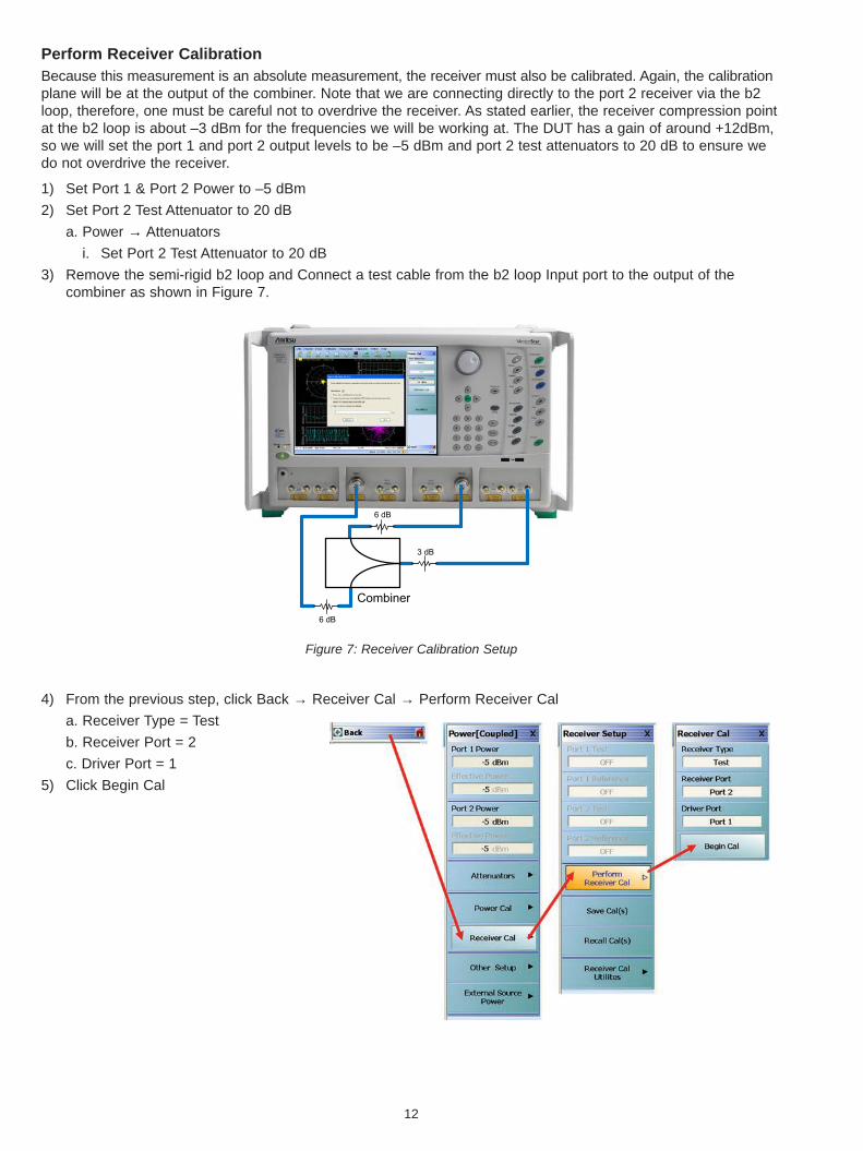
4) From the previous step, click Back → Receiver Cal → Perform Receiver Cal
a. Receiver Type = Test
b. Receiver Port = 2
c. Driver Port = 1
5) Click Begin Cal
Perform Receiver CalibrationBecause this measurement is an absolute measurement, the receiver must also be calibrated. Again, the calibration plane will be at the output of the combiner. Note that we are connecting directly to the port 2 receiver via the b2 loop, therefore, one must be careful not to overdrive the receiver. As stated earlier, the receiver compression point at the b2 loop is about –3 dBm for the frequencies we will be working at. The DUT has a gain of around +12dBm, so we will set the port 1 and port 2 output levels to be –5 dBm and port 2 test attenuators to 20 dB to ensure we do not overdrive the receiver.
1) Set Port 1 & Port 2 Power to –5 dBm
2) Set Port 2 Test Attenuator to 20 dB
a. Power → Attenuators
i. Set Port 2 Test Attenuator to 20 dB
3) Remove the semi-rigid b2 loop and Connect a test cable from the b2 loop Input port to the output of the combiner as shown in Figure 7.
Combiner
6 dB
6 dB
3 dB
Figure 7: Receiver Calibration Setup
13
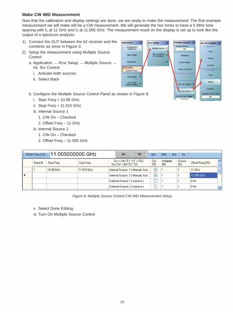
Make CW IMD MeasurementNow that the calibration and display settings are done, we are ready to make the measurement. The first example measurement we will make will be a CW measurement. We will generate the two tones to have a 5 MHz tone spacing with f1 at 11 GHz and f2 at 11.005 GHz. The measurement result on the display is set up to look like the output of a spectrum analyzer.
1) Connect the DUT between the b2 receiver and the combiner as show in Figure 3.
2) Setup the measurement using Multiple Source Control
a. Application → Rcvr Setup → Multiple Source → Int. Src Control
i. Activate both sources
ii. Select Back
b. Configure the Multiple Source Control Panel as shown in Figure 8.
i. Start Freq = 10.99 GHz
ii. Stop Freq = 11.015 GHz
iii. Internal Source 1
1. CW On – Checked
2. Offset Freq – 11 GHz
iv. Internal Source 2
1. CW On – Checked
2. Offset Freq – 11.005 GHz
Figure 8: Multiple Source Control CW IMD Measurement Setup
v. Select Done Editing.
vi. Turn On Multiple Source Control
14
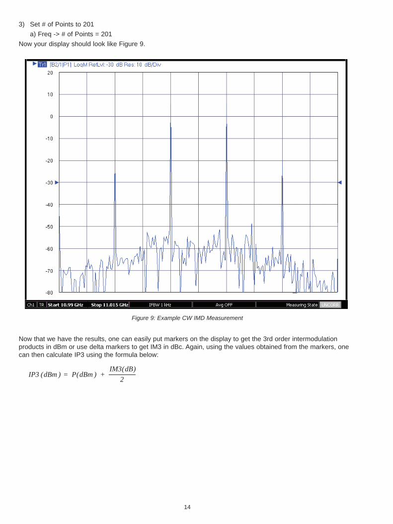
3) Set # of Points to 201
a) Freq -> # of Points = 201
Now your display should look like Figure 9.
Figure 9: Example CW IMD Measurement
Now that we have the results, one can easily put markers on the display to get the 3rd order intermodulation products in dBm or use delta markers to get IM3 in dBc. Again, using the values obtained from the markers, one can then calculate IP3 using the formula below:
∗ 1 + ∗ 2
2f1 + f2 + f1 1, 2f1 – f2, 2f2 , and f
3rd order intermodulation product
–2f2
3 = + | 32
|
3 = +10 + |
|
( 20 – [−40 ]) 2 |
|
= +10 + 60
2
= +40
IP3 (dBm ) = P
P
OIP3P P
(dBm ) + IM3(dB)
2
3 = 0 + |
|
(10 – [−
−
70 ]) 2 |
|
3 = =
0 + |(+10 – [−70 ])
2|
= 0 + 80
2
= +40
= 3
+ | 32 | + | 3
2 | and
15
Make Swept IMD MeasurementCW IMD measurements can also be made using a spectrum analyzer instead of a VNA using the same approach. The advantage VNAs have over spectrum analyzers in making IMD measurements is the ability to make swept frequency as well as swept power IMD measurements. Using the VectorStar’s Multiple Source Control menu, it is very easy to setup a swept frequency IMD measurement.
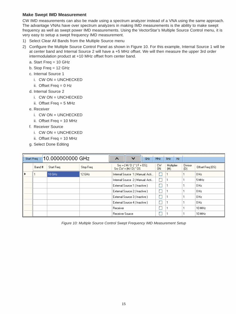
1) Select Clear All Bands from the Multiple Source menu
2) Configure the Multiple Source Control Panel as shown in Figure 10. For this example, Internal Source 1 will be at center band and Internal Source 2 will have a +5 MHz offset. We will then measure the upper 3rd order intermodulation product at +10 MHz offset from center band.
a. Start Freq = 10 GHz
b. Stop Freq = 12 GHz
c. Internal Source 1
i. CW ON = UNCHECKED
ii. Offset Freq = 0 Hz
d. Internal Source 2
i. CW ON = UNCHECKED
ii. Offset Freq = 5 MHz
e. Receiver
i. CW ON = UNCHECKED
ii. Offset Freq = 10 MHz
f. Receiver Source
i. CW ON = UNCHECKED
ii. Offset Freq = 10 MHz
g. Select Done Editing
Figure 10: Multiple Source Control Swept Frequency IMD Measurement Setup
16
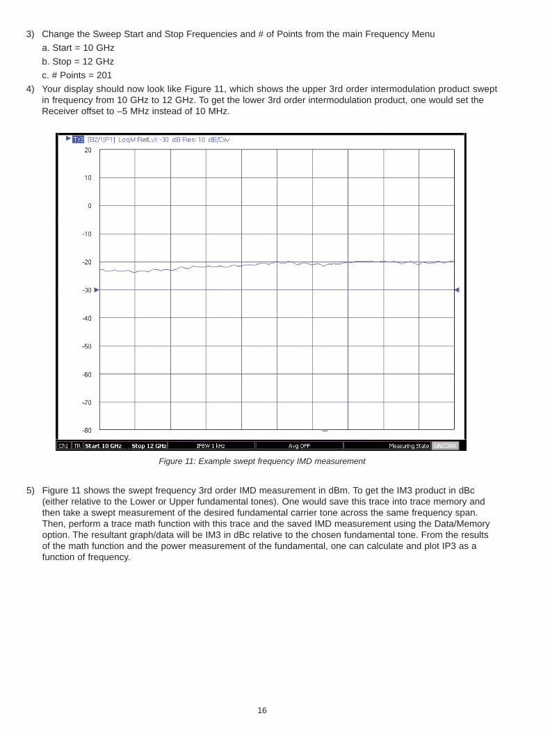
3) Change the Sweep Start and Stop Frequencies and # of Points from the main Frequency Menu
a. Start = 10 GHz
b. Stop = 12 GHz
c. # Points = 201
4) Your display should now look like Figure 11, which shows the upper 3rd order intermodulation product swept in frequency from 10 GHz to 12 GHz. To get the lower 3rd order intermodulation product, one would set the Receiver offset to –5 MHz instead of 10 MHz.
Figure 11: Example swept frequency IMD measurement
5) Figure 11 shows the swept frequency 3rd order IMD measurement in dBm. To get the IM3 product in dBc (either relative to the Lower or Upper fundamental tones). One would save this trace into trace memory and then take a swept measurement of the desired fundamental carrier tone across the same frequency span. Then, perform a trace math function with this trace and the saved IMD measurement using the Data/Memory option. The resultant graph/data will be IM3 in dBc relative to the chosen fundamental tone. From the results of the math function and the power measurement of the fundamental, one can calculate and plot IP3 as a function of frequency.
17
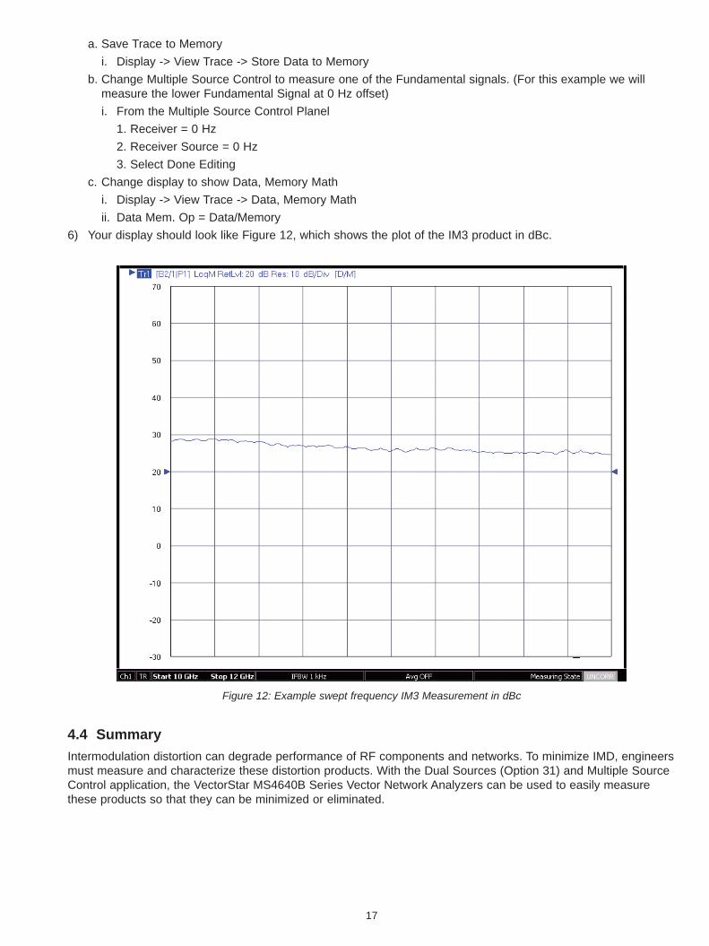
a. Save Trace to Memory
i. Display -> View Trace -> Store Data to Memory
b. Change Multiple Source Control to measure one of the Fundamental signals. (For this example we will measure the lower Fundamental Signal at 0 Hz offset)
i. From the Multiple Source Control Planel
1. Receiver = 0 Hz
2. Receiver Source = 0 Hz
3. Select Done Editing
c. Change display to show Data, Memory Math
i. Display -> View Trace -> Data, Memory Math
ii. Data Mem. Op = Data/Memory
6) Your display should look like Figure 12, which shows the plot of the IM3 product in dBc.
Figure 12: Example swept frequency IM3 Measurement in dBc
4.4 Summary
Intermodulation distortion can degrade performance of RF components and networks. To minimize IMD, engineers must measure and characterize these distortion products. With the Dual Sources (Option 31) and Multiple Source Control application, the VectorStar MS4640B Series Vector Network Analyzers can be used to easily measure these products so that they can be minimized or eliminated.
® Anritsu All trademarks are registered trademarks of their respective companies. Data subject to change without notice. For the most recent specifications visit: www.anritsu.com
Anritsu utilizes recycled paper and environmentally conscious inks and toner.
• United States Anritsu Company1155 East Collins Boulevard, Suite 100, Richardson, TX, 75081 U.S.A. Toll Free: 1-800-267-4878 Phone: +1-972-644-1777 Fax: +1-972-671-1877
• Brazil Anritsu Electrônica Ltda.Praça Amadeu Amaral, 27 - 1 Andar 01327-010 - Bela Vista - São Paulo - SP - Brazil Phone: +55-11-3283-2511 Fax: +55-11-3288-6940
• Russia Anritsu EMEA Ltd. Representation Office in RussiaTverskaya str. 16/2, bld. 1, 7th floor. Moscow, 125009, Russia Phone: +7-495-363-1694 Fax: +7-495-935-8962
• Spain Anritsu EMEA Ltd. Representation Office in SpainEdificio Cuzco IV, Po. de la Castellana, 141, Pta. 8 28046, Madrid, Spain Phone: +34-915-726-761 Fax: +34-915-726-621
• United Arab Emirates Anritsu EMEA Ltd. Dubai Liaison OfficeP O Box 500413 - Dubai Internet City Al Thuraya Building, Tower 1, Suite 701, 7th floor Dubai, United Arab Emirates Phone: +971-4-3670352 Fax: +971-4-3688460
• India Anritsu India Pvt Ltd.2nd & 3rd Floor, #837/1, Binnamangla 1st Stage, Indiranagar, 100ft Road, Bangalore - 560038, India Phone: +91-80-4058-1300 Fax: +91-80-4058-1301
• P. R. China (Shanghai) Anritsu (China) Co., Ltd.27th Floor, Tower A, New Caohejing International Business Center No. 391 Gui Ping Road Shanghai, Xu Hui Di District, Shanghai 200233, P.R. China Phone: +86-21-6237-0898 Fax: +86-21-6237-0899
• P. R. China (Hong Kong) Anritsu Company Ltd.Unit 1006-7, 10/F., Greenfield Tower, Concordia Plaza, No. 1 Science Museum Road, Tsim Sha Tsui East, Kowloon, Hong Kong, P. R. China Phone: +852-2301-4980 Fax: +852-2301-3545
• Japan Anritsu Corporation8-5, Tamura-cho, Atsugi-shi, Kanagawa, 243-0016 Japan Phone: +81-46-296-1221 Fax: +81-46-296-1238
• Korea Anritsu Corporation, Ltd.5FL, 235 Pangyoyeok-ro, Bundang-gu, Seongnam-si, Gyeonggi-do, 463-400 Korea Phone: +82-31-696-7750 Fax: +82-31-696-7751
• Australia Anritsu Pty Ltd.Unit 21/270 Ferntree Gully Road, Notting Hill, Victoria 3168, Australia Phone: +61-3-9558-8177 Fax: +61-3-9558-8255
• Taiwan Anritsu Company Inc.7F, No. 316, Sec. 1, Neihu Rd., Taipei 114, Taiwan Phone: +886-2-8751-1816 Fax: +886-2-8751-1817