Inspection of Integrated Circuit Databases through Reticle and Wafer Simulation: An Integrated Approach to Design for Manufacturing (DFM) William Howard *a , Jaione Tirapu Azpiroz b , Yalin Xiong c , Chris Mack a , Gaurav Verma c , William Volk c , Harold Lehon c , Yunfei Deng c , Rui-fang Shi c , James Culp b , Scott Mansfield b a KLA-Tencor, 8834 North Capital of Texas Highway, Suite 301, Austin, Texas 78759, USA b IBM Microelectronics, 2070 Route 52, Hopewell Junction, New York 12533, USA c KLA-Tencor, 160 Rio Robles, San Jose, California 95134, USA ABSTRACT The present approach to Optical Proximity Correction (OPC) verification has evolved from a number of separate inspection strategies. OPC decoration is verified by a design rule or optical rule checker, the reticle is verified by a reticle inspection system, and the final wafers are verified by wafer inspection and metrology tools. Each verification step looks at a different representation of the desired device pattern with little or no data flowing between them. In this paper, we will report on a new inspection system called DesignScan that connects the data between the various abstraction layers. DesignScan inspects the OPC decorated design by simulating how the design will be transferred to the reticle layer and how that reticle will be imaged into resist across the full focus-exposure process window. The simulated images are compared to the desired pattern and defect detection algorithms are applied to determine if any unacceptable variations in the pattern occurs within the nominal process window. The end result is a new paradigm in design verification, moving beyond OPC verification at the design plane to process window verification at the wafer plane where it really matters. We will demonstrate the application of DesignScan to inspect full chip designs that utilized different Resolution Enhancement Technique (RET) and OPC methods. In doing so, we’ll demonstrate that DesignScan can identify the relative strengths and weaknesses of each methodology by highlighting areas of weak process window for each approach. We will present experimental wafer level results to verify the accuracy of the defect predictions. Keywords: DesignScan, DFM, process window, PROLITH, simulation 1. INTRODUCTION 1.1. Pattern Dependent Yield Loss In previous design nodes, yield loss was mainly driven by random effects such as defect density. Since then, systematic effects have become dominant and one of these is Pattern Dependent Yield Loss (PDYL) 1,2 . PDYL is characterized by one or more of the patterns on the device layer failing prematurely in the process window. These patterns, which are called “weak designs” or “hot spots”, are most sensitive to changes in focus and exposure and, therefore, they have smaller process windows. Since the effective process window is only as large as the intersection of all the component pattern process windows, yield loss results. This phenomenon is illustrated in Figure 1 that shows the diminishing of the process window caused by two such weak designs. *[email protected]; phone 512-231-4249; fax 512-346-9542; 8834 N. Capital of Texas Highway, Suite 301, Austin, TX 78759 Design and Process Integration for Microelectronic Manufacturing III, edited by Lars W. Liebmann, Proceedings of SPIE Vol. 5756 (SPIE, Bellingham, WA, 2005) · 0277-786X/05/$15 · doi: 10.1117/12.604698 61 Downloaded From: http://proceedings.spiedigitallibrary.org/ on 05/06/2014 Terms of Use: http://spiedl.org/terms
Transcript
Inspection of Integrated Circuit Databases through Reticle and Wafer Simulation: An Integrated Approach to Design for Manufacturing
(DFM)
William Howard*a, Jaione Tirapu Azpirozb, Yalin Xiongc, Chris Macka, Gaurav Vermac, William Volkc, Harold Lehonc, Yunfei Dengc, Rui-fang Shic, James Culpb, Scott Mansfieldb
aKLA-Tencor, 8834 North Capital of Texas Highway, Suite 301, Austin, Texas 78759, USA
bIBM Microelectronics, 2070 Route 52, Hopewell Junction, New York 12533, USA cKLA-Tencor, 160 Rio Robles, San Jose, California 95134, USA
ABSTRACT
The present approach to Optical Proximity Correction (OPC) verification has evolved from a number of separate inspection strategies. OPC decoration is verified by a design rule or optical rule checker, the reticle is verified by a reticle inspection system, and the final wafers are verified by wafer inspection and metrology tools. Each verification step looks at a different representation of the desired device pattern with little or no data flowing between them. In this paper, we will report on a new inspection system called DesignScan that connects the data between the various abstraction layers. DesignScan inspects the OPC decorated design by simulating how the design will be transferred to the reticle layer and how that reticle will be imaged into resist across the full focus-exposure process window. The simulated images are compared to the desired pattern and defect detection algorithms are applied to determine if any unacceptable variations in the pattern occurs within the nominal process window. The end result is a new paradigm in design verification, moving beyond OPC verification at the design plane to process window verification at the wafer plane where it really matters. We will demonstrate the application of DesignScan to inspect full chip designs that utilized different Resolution Enhancement Technique (RET) and OPC methods. In doing so, we’ll demonstrate that DesignScan can identify the relative strengths and weaknesses of each methodology by highlighting areas of weak process window for each approach. We will present experimental wafer level results to verify the accuracy of the defect predictions. Keywords: DesignScan, DFM, process window, PROLITH, simulation
1. INTRODUCTION
1.1. Pattern Dependent Yield Loss In previous design nodes, yield loss was mainly driven by random effects such as defect density. Since then, systematic effects have become dominant and one of these is Pattern Dependent Yield Loss (PDYL) 1,2 . PDYL is characterized by one or more of the patterns on the device layer failing prematurely in the process window. These patterns, which are called “weak designs” or “hot spots”, are most sensitive to changes in focus and exposure and, therefore, they have smaller process windows. Since the effective process window is only as large as the intersection of all the component pattern process windows, yield loss results. This phenomenon is illustrated in Figure 1 that shows the diminishing of the process window caused by two such weak designs. *[email protected]; phone 512-231-4249; fax 512-346-9542; 8834 N. Capital of Texas Highway, Suite 301, Austin, TX 78759
Design and Process Integration for Microelectronic Manufacturing III,edited by Lars W. Liebmann, Proceedings of SPIE Vol. 5756(SPIE, Bellingham, WA, 2005) · 0277-786X/05/$15 · doi: 10.1117/12.604698
61
Downloaded From: http://proceedings.spiedigitallibrary.org/ on 05/06/2014 Terms of Use: http://spiedl.org/terms
Figure 1: The entitlement process window (depicted as a solid ellipse) is that which is expected based on the process capability. When “weak patterns” or “hot spots” exist in the design, their process windows (depicted as two dashed ellipses) are smaller than the entitlement process window. Since the actual process window is the intersection of all component process windows (shown as the shaded region), PDYL results. The general approach to reduce PDYL is to employ strategies that bring process and lithography knowledge into the design and Resolution Enhancement Techniques (RET) processes in the hope that this information can improve yield and prevent such weak designs. These approaches have, in fact, been very useful but not completely successful, and PDYL is still problematic3. Any successful Design for Manufacturing (DFM) system must have two components. First, it must be possible to detect and isolate problems. Second, it must facilitate the resolution of the problems. Several point solutions might form a working DFM system if they are integrated and their various strengths combined in a constructive way. As an example, reticle inspection systems play a vital role to ensure that the desired design is properly transferred to the reticle. However, these inspection systems do not verify that the design will result in high yield for the given lithography process. So, reticle inspection should be combined with a system that checks lithographic performance through the process window. This paper briefly reviews two existing DFM technologies. Then, we discuss a new approach to evaluating a design for process window sensitivity that can strengthen the suite of tools available for a complete DFM solution.
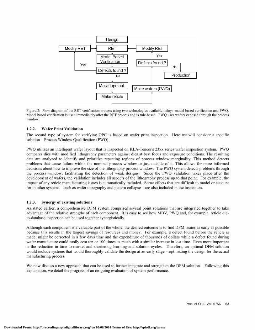
1.2. Current solutions for design validation As a starting point for reviewing currently available DFM solutions, it is helpful to examine the flow of information through the design process. Figure 2 shows a simple block diagram containing some important stages.
1.2.1. Model Based Verification One technology used to validate the post-RET design is called Model Based Verification (MBV). As shown in Figure 2, MBV systems can be used in the process flow immediately following RET and, therefore, one of their strengths is that problems are found immediately before further investments of resources. In general, this optical inline checking technique works by parsing the input design edges into small edges. Then each edge is used to find the simulated process response from a calibrated model. This simulated process response is then checked with standard DRC tools to look for conditions approaching fail limits. For cost savings, typically the same vendor is used for Optical Proximity Correction (OPC) and MBV. These systems are integrated into the design flow that facilitates feedback of errors and correction of the OPC decoration process.
Dose
Focus
Entitlement process window
Actual process window
62 Proc. of SPIE Vol. 5756
Downloaded From: http://proceedings.spiedigitallibrary.org/ on 05/06/2014 Terms of Use: http://spiedl.org/terms
Figure 2: Flow diagram of the RET verification process using two technologies available today: model based verification and PWQ. Model based verification is used immediately after the RET process and is rule-based. PWQ uses wafers exposed through the process window.
1.2.2. Wafer Print Validation The second type of system for verifying OPC is based on wafer print inspection. Here we will consider a specific solution – Process Window Qualification (PWQ). PWQ utilizes an intelligent wafer layout that is inspected on KLA-Tencor's 23xx series wafer inspection system. PWQ compares dies with modified lithography parameters against dies at best focus and exposure conditions. The resulting data are analyzed to identify and prioritize repeating regions of process window marginality. This method detects problems that cause failure within the nominal process window or just outside of it. This allows for more informed decisions about how to improve the size of the lithography process window. The PWQ system detects problems through the process window, facilitating the detection of weak designs. Since the PWQ validation takes place after the development of wafers, the validation includes all aspects of the lithography process up to that point. For example, the impact of any reticle manufacturing issues is automatically included. Some effects that are difficult to model or account for in other systems – such as wafer topography and pattern collapse – are also included in the inspection.
1.2.3. Synergy of existing solutions As stated earlier, a comprehensive DFM system comprises several point solutions that are integrated together to take advantage of the relative strengths of each component. It is easy to see how MBV, PWQ and, for example, reticle die-to-database inspection can be used together synergistically. Although each component is a valuable part of the whole, the desired outcome is to find DFM issues as early as possible because this results in the largest savings of resources and money. For example, a defect found before the reticle is made, might be corrected in a few days time and the expenditure of thousands of dollars while a defect found during wafer manufacture could easily cost ten or 100 times as much with a similar increase in lost time. Even more important is the reduction in time-to-market and shortening learning and solution cycles. Therefore, an optimal DFM solution would include systems that would thoroughly validate the design at an early stage – optimizing the design for the actual manufacturing process. We now discuss a new approach that can be used to further integrate and strengthen the DFM solution. Following this explanation, we detail the progress of an on-going evaluation of system performance.
Proc. of SPIE Vol. 5756 63
Downloaded From: http://proceedings.spiedigitallibrary.org/ on 05/06/2014 Terms of Use: http://spiedl.org/terms
2. DESIGNSCAN DesignScanTM is a new inspection system from KLA-Tencor that detects pattern dependent (feature-based) systematic defects in the lithography process window of the post RET design. The inspection is accomplished by simulating the transfer of the design to the reticle plane and the subsequent projection of the reticle image into photoresist. The simulations are conducted at nominal conditions and at several focus-exposure points through the process window. The best focus and exposure condition is the reference for comparison of all other off-focus and exposure conditions. Each simulation within the process window is compared to the one at nominal conditions to detect any unacceptable variation in pattern fidelity. It is important to recognize that DesignScan assumes the best focus and exposure condition has been verified by MBV prior to a DesignScan inspection. This approach is represented in Figure 3.
Figure 3: A depiction of the DesignScan inspection paradigm. A patch of the final post RET design is simulated at nominal focus and exposure conditions (center image) and forms the reference. The patch is then simulated at a wide range of focus and exposure conditions away from nominal conditions (the images on the perimeter) and each of these simulated results is compared with the nominal. The DesignScan system consists of hardware and software components, many of which are based on the KLA-Tencor TeraScanTM die-to-database reticle inspection system and the KLA-Tencor PROLITHTM simulation software. Prior to the DesignScan inspection, the post-RET/OPC designs are accessed by the TeraPrepTM subsystem and converted to a format optimized for inspection throughput. At run time, the converted design is segmented into patches and fed to the proprietary image computer which is used for both the simulation of the design patches and the detection of defects. The image computer is a multiple-processor based supercomputer capable of simulating multiple jobs simultaneously. Design patches that fail within the process window are noted as defective. Defect reports are sent to the operator console which is also used for inspection setup and review. The system hardware components are shown in Figure 4. The simulation models three distinct steps in the lithography process: the transfer of the pattern to the reticle, the formation of the aerial image and the formation of the resist image. The model for the reticle manufacture process is based on TeraScan technology used for die-to-database reticle inspection. The aerial image formation uses a vector imaging model. The resist image formation and development are based on a proprietary fast resist model and PROLITH technology.
64 Proc. of SPIE Vol. 5756
Downloaded From: http://proceedings.spiedigitallibrary.org/ on 05/06/2014 Terms of Use: http://spiedl.org/terms
Figure 4: The DesignScan system hardware. The operator console is shown on the left. The TeraPrep sub-system is shown in the dark chassis and the image computer is shown on the right. A second operator console connected to the TeraPrep is not shown. Each of the three models is calibrated or specified separately and, by design, they are independent and interchangeable. Physics-based models are used to simulate reticle images from the design. The images are compared with reticle SEM images to extract model parameters. The aerial image model is specified by providing the following basic illumination parameters: illumination wavelength, parametric or measured source shape, and objective lens NA. The resist model is calibrated by matching physical parameters to tuning data. The tuning data consists of focus-exposure CD data from 1-D lines and spaces at various pitches and sizes. The tuning process has evolved from that used in previous research 4. At runtime, the user creates a recipe through a menu-driven Graphical User Interface (GUI) shown in Figure 5. It is at this point that the design to be inspected and the previously calibrated or specified models are recalled. The user also selects the range of focus and exposure conditions to be used in the inspection during this step. Each focus and exposure point can be defined individually and need not be a regular array of points. Any segment of the design that has been converted to the DesignScan format can be inspected. The system supports the definition of multiple inspection areas each of which can have independent defect sensitivity settings. The runtime setup process typically takes less than 10 minutes. At the end of the recipe definition, the inspection process begins and each patch of the design is processed through the simulation and defect detection models. As explained earlier and depicted in Figure 3, it is at this stage that the various simulations for each design patch are compared to the simulation at nominal conditions. The defect detection algorithm checks for the following types of defects: bridges, breaks, extra and missing printed features, minimum resist width and minimum space width. The defect detection is based on any topographical change between a test resist profile and the reference resist profile. The minimum resist width and minimum space width defects are those that are close to failing. These defects warn the operator of locations in the design that might fail either later in the process (such as during etch) or if focus and/or exposure deviate any further from the nominal conditions. A proprietary defect binning model is used to group all identical defects. This greatly improves review efficiency and leverages the hierarchy of the design. The efficiencies gained by the defect binning system will be dependent on the hierarchy of the design and many other factors. In the initial tests of the system, using the candidate designs described below in Section 3, a reduction in the number of unique defects by a factor of seven has been observed. Review can occur after or concurrent with the inspection. The defect review application shown in Figure 6 can be used to display a wide range of information and the display is user-configurable.
Proc. of SPIE Vol. 5756 65
Downloaded From: http://proceedings.spiedigitallibrary.org/ on 05/06/2014 Terms of Use: http://spiedl.org/terms
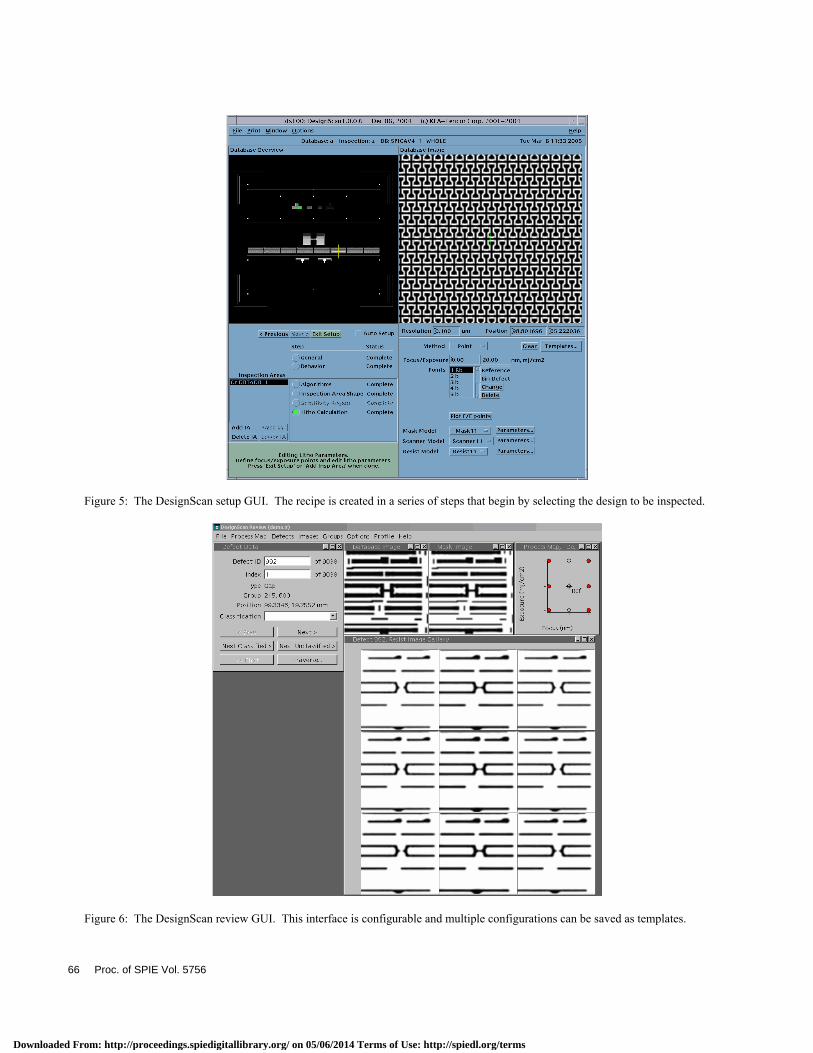
Figure 5: The DesignScan setup GUI. The recipe is created in a series of steps that begin by selecting the design to be inspected.
Figure 6: The DesignScan review GUI. This interface is configurable and multiple configurations can be saved as templates.
66 Proc. of SPIE Vol. 5756
Downloaded From: http://proceedings.spiedigitallibrary.org/ on 05/06/2014 Terms of Use: http://spiedl.org/terms
The inspection throughput is a function of the number of focus-exposure points specified for validation and the size of the inspection area. For a 5x7 focus-exposure array (34 test simulations and one simulation at nominal conditions for the reference) the system will inspect an 8mm x 8mm patch (wafer scale) in approximately two hours. DesignScan inspections are expected to be used as a final verification before the manufacture of the reticle. At this point in the process flow (see Figure 2) the design has already passed MBV at the nominal conditions. As stated above, it is at this point that the information is most valuable because solutions can be implemented before the expense of making reticles or wafers has been incurred. But, more importantly, any issues can be resolved early in the process reducing critical cycle time and improving time to market.
3. EXPERIMENTS AND RESULTS In this section we present the results of the on-going joint evaluation of DesignScan performance by IBM and KLA-Tencor. The various aspects of the evaluation are presented and analyzed. The results are organized based on three different perspectives: process model calibration accuracy, inspection throughput and inspection capability.
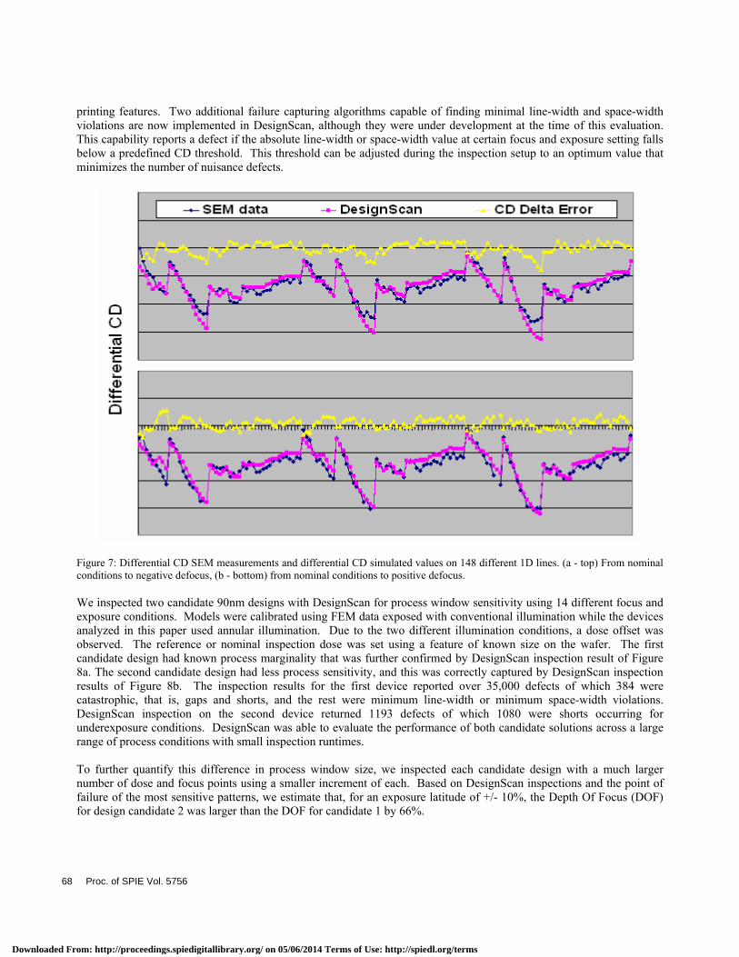
3.1. Process Model Calibration Accuracy The current mask and wafer models balance the tradeoff between accuracy and calibration effort. Current calibration procedures require detailed wafer linewidth measurements for three simple patterns: an isolated line, and isolated space and a dense line/space pattern. Detailed Bossung curves across a range of focus and dose variation were provided through Scanning Electron Microscope (SEM) wafer CD measurements to calibrate a 90nm gate level at 193nm wavelength. Mask models were calibrated using reticle SEM images for more accurate modeling of the nonlinearities of the mask manufacturing process and corner rounding. To facilitate DesignScan’s main use of detecting areas of weak process window, DesignScan must accurately predict how the resist images changes as focus and exposure vary in the process window. Hence, we focused on evaluating the accuracy of the differential CD predicted by DesignScan models compared to a standard of wafer data measured using a CD SEM. For this study, we used a number of test patterns including 1D lines through pitch and 2D line ends. Two sets of data were collected for the differential CD from nominal conditions to positive defocus and negative defocus values. Additional measurements throughout a range of dose at nominal focus were also obtained for this accuracy assessment. Figures 7(a) and 7(b) display a sample of the differential CD measurements on 1D lines from nominal conditions to the out of focus conditions that exhibit a reasonably good agreement with the differential CD predicted by DesignScan models at the same conditions. Based on the SEM data, the differential CD accuracy of DesignScan was found to be bounded by +/-5nm (3 sigma) for 1D patterns. Regarding the 2D line ends, the differential CD accuracy of DesignScan was bounded by +/-15nm (3 sigma).
3.2. Inspection Throughput Current versions of the algorithms are not yet optimized for full speed capability. Nevertheless, the current tool capability allowed for an average of 5 ½ hours runtime on a full 90nm chip of 7mm by 9mm area (wafer scale) at 14 different focus and exposure conditions. Since the time of these inspections, system improvements have been made and the inspection throughput is close to the target capability of two hours for 35 different focus and exposure conditions over an 8mm x 8mm area (wafer scale). More throughput improvements are planned.
3.3. Inspection Capability The accuracy and efficiency of the inspection algorithm is of critical importance to enable effective optimization of the design for the lithographic process. The accuracy is measured by its capability to capture 100% of the failures limiting the process window and the efficiency is assessed in terms of the number of nuisance defects reported. The current version of DesignScan is able to detect catastrophic defects, which are identified as shorts or opens and missing or extra
Proc. of SPIE Vol. 5756 67
Downloaded From: http://proceedings.spiedigitallibrary.org/ on 05/06/2014 Terms of Use: http://spiedl.org/terms
printing features. Two additional failure capturing algorithms capable of finding minimal line-width and space-width violations are now implemented in DesignScan, although they were under development at the time of this evaluation. This capability reports a defect if the absolute line-width or space-width value at certain focus and exposure setting falls below a predefined CD threshold. This threshold can be adjusted during the inspection setup to an optimum value that minimizes the number of nuisance defects.
Figure 7: Differential CD SEM measurements and differential CD simulated values on 148 different 1D lines. (a - top) From nominal conditions to negative defocus, (b - bottom) from nominal conditions to positive defocus. We inspected two candidate 90nm designs with DesignScan for process window sensitivity using 14 different focus and exposure conditions. Models were calibrated using FEM data exposed with conventional illumination while the devices analyzed in this paper used annular illumination. Due to the two different illumination conditions, a dose offset was observed. The reference or nominal inspection dose was set using a feature of known size on the wafer. The first candidate design had known process marginality that was further confirmed by DesignScan inspection result of Figure 8a. The second candidate design had less process sensitivity, and this was correctly captured by DesignScan inspection results of Figure 8b. The inspection results for the first device reported over 35,000 defects of which 384 were catastrophic, that is, gaps and shorts, and the rest were minimum line-width or minimum space-width violations. DesignScan inspection on the second device returned 1193 defects of which 1080 were shorts occurring for underexposure conditions. DesignScan was able to evaluate the performance of both candidate solutions across a large range of process conditions with small inspection runtimes. To further quantify this difference in process window size, we inspected each candidate design with a much larger number of dose and focus points using a smaller increment of each. Based on DesignScan inspections and the point of failure of the most sensitive patterns, we estimate that, for an exposure latitude of +/- 10%, the Depth Of Focus (DOF) for design candidate 2 was larger than the DOF for candidate 1 by 66%.
68 Proc. of SPIE Vol. 5756
Downloaded From: http://proceedings.spiedigitallibrary.org/ on 05/06/2014 Terms of Use: http://spiedl.org/terms
a) b)
Figure 8: DesignScan full chip inspection defect map on a design with (a) marginal process window and (b) less process sensitivity. The evaluation of the accuracy of the results was critical for this work. Hence we confirmed on both designs that DesignScan was able to detect all known catastrophic defects within the process window. These catastrophic defects were confirmed by SEM images obtained from wafers exposed according to a matrix of focus and dose conditions. Two examples of catastrophic line gaps detected by DesignScan and confirmed with SEM images can be seen in Figures 9 and 10, which also illustrate the Inspection Review GUI resist image gallery of the corresponding defect. Figure 11 displays an example of catastrophic bridge or short defect occurring at lower dose. These SEM images also show some of the lines collapsing at large negative defocus. This effect, which is presumably produced by a thinning at the bottom of the resist profile, is not being modeled by the current version of DesignScan and, therefore, this type of defect could not be captured. Modeling of this resist failure mechanism will be discussed in the future work section.
Figure 9: Inspection Review GUI along with SEM image confirmation displaying one example of catastrophic gaps. The image gallery in this example shows the resist image predicted by DesignScan at 14 different focus/exposure conditions. The nominal condition is shown outlined in a blue dashed box. The blue ellipses circle the defect at points for which we have confirmed the results using wafer print studies.
Proc. of SPIE Vol. 5756 69
Downloaded From: http://proceedings.spiedigitallibrary.org/ on 05/06/2014 Terms of Use: http://spiedl.org/terms
Figure 10: SEM confirmation of a second example of catastrophic gaps. The top SEM image on the right validates the nominal focus/exposure resist image prediction of design scan. The middle image confirms the defective location to which it points. The bottom SEM image affirms one of the non-defective predictions.
Figure 11: Resist image gallery and SEM image confirmation of a bridging defect. It is important to note that this defect does not occur a the corners of the process window. In addition to the catastrophic type of defects, DesignScan detected numerous minimum line-width violations. This capability checks for absolute line-width values falling below a certain threshold at each focus and dose setting and, as a result, it is very sensitive to model inaccuracies. An example of a minimum line-width violation was found on an H-bar shown in Figure 12. The cross member of this H-bar is slightly shorter than the one in Figure 9. According to DesignScan results, this line remains standing at the extremes of the process window, but it gets thin and eventually becomes problematic. This same behavior was observed in the wafer SEM images, also shown in Figure 12. Overall qualitative analysis of SEM images confirmed that those locations identified as minimum line-width violations were potential process window limiters. These initial results validated the performance of the minimum line-width detectors in a qualitative manner. However, no linewidth measurement was taken that would allow a more quantitative analysis, and a more thorough evaluation of this capability is being carried out.
70 Proc. of SPIE Vol. 5756
Downloaded From: http://proceedings.spiedigitallibrary.org/ on 05/06/2014 Terms of Use: http://spiedl.org/terms
Figure 12: Qualitative confirmation against SEM images of a defect reported by DesignScan as a minimum line-width violation. The bottom SEM image on the right confirms the DesignScan resist image prediction at nominal conditions.
4. DISCUSSION Initial evaluation of DesignScan capabilities showed satisfactory results in terms of the model differential accuracy, inspection accuracy and inspection throughput. DesignScan capability to quickly verify different RET solutions across the entire process window by detecting process limiting geometries was demonstrated. Overall, there was good qualitative correlation to SEM images from printed wafers through the process window, and more quantitative work continues. A comparison of the defects shown in Figures 9 and 12, shows that the designs are not significantly different and the context around the designs is also similar. The main difference between the two designs is the length of the cross member of the H-structure. However, the process window sensitivities of the two design segments are quite different. This enforces the concept that seemingly small differences in design can have significantly different lithographic performance across the process window. To evaluate the lithographic performance of the design across the process window, one must use many focus and exposure points and not merely those at the corners of the process window. In particular, the bridging defect shown in Figure 11 fails at an under-exposure condition only when at nominal focus – so this defect would not have been caught had only the corners of the process window been checked. Further, were only a few focus/exposure conditions used, it would not be as easy to differentiate between a weak pattern that fails only at the extremes of the process window and patterns that are even “more weak” that fail closer to nominal conditions. The inclusion of multiple focus/exposure points facilitates a more detailed analysis to find the most critically weak patterns.
5. CONCLUSIONS These initial results are viewed as proof of DesignScan’s potential to quickly evaluate the DFM quality of final designs at an early stage when corrections can be made most cost-effectively. The system throughput is such that faster learning cycles for RET development should be possible leading quickly to the reduction of PDYL.
Proc. of SPIE Vol. 5756 71
Downloaded From: http://proceedings.spiedigitallibrary.org/ on 05/06/2014 Terms of Use: http://spiedl.org/terms
6. FUTURE WORK Work is in progress on the tuning of additional processes to be used to inspect several 90nm and 65nm designs for various layers. This wide range of use provides valuable information to improve DesignScan performance and functionality. One important future challenge that has been identified is the prediction of resist feature collapse. DesignScan does not currently have this functionality. This capability will be a focus of work over the next several months. At present, this enforces the synergistic nature of DFM as other systems (such as PWQ) are capable of finding such defects. The current best practice is to understand, leverage and integrate each system’s strengths for a complete DFM strategy. Several new enhancements to the system, such as a defect binning capability, were too recent to be included in this study. We plan to evaluate their effectiveness and report on them in the future.
ACKNOWLEDGMENTS The authors acknowledge the contributions of IBM’s OPC team for providing the design data used in this study and the lithography team for providing wafer verification data. We also want to thank the entire KLA-Tencor DesignScan R&D and engineering team.
REFERENCES 1. R. Radojcic and M. Rencher, “Old Rules No Longer Apply,” EETimes, April 29, 2003. 2. L.Peters, “Roadmap Challenges Underscore Troubling Trend in Yields,” Semiconductor International, February 1,
2004. 3. L. Peters, “Demystifying Design-for-Yield,” Semiconductor International, July 1, 2004. 4. S. Jug, R. Huang, J.D. Byers, and C.A. Mack, “Automatic Calibration of Lithography Simulation Parameters,”
Lithography for Semiconductor Manufacturing II, Proc., SPIE 4404, pp. 380-395, 2001.
72 Proc. of SPIE Vol. 5756
Downloaded From: http://proceedings.spiedigitallibrary.org/ on 05/06/2014 Terms of Use: http://spiedl.org/terms