222
Intel ® 815E Chipset Platform Design Guide June 2000 Document Reference Number: 298234-001 R
Intel® 815E Chipset Platform Design Guide
June 2000
Document Reference Number: 298234-001
R
Intel® 815E Chipset Platform
R
2 Design Guide
Information in this document is provided in connection with Intel products. No license, express or implied, by estoppel or otherwise, to any intellectual property rights is granted by this document. Except as provided in Intels Terms and Conditions of Sale for such products, Intel assumes no liability whatsoever, and Intel disclaims any express or implied warranty, relating to sale and/or use of Intel products including liability or warranties relating to fitness for a particular purpose, merchantability, or infringement of any patent, copyright or other intellectual property right. Intel products are not intended for use in medical, lifesaving, or life-sustaining applications.
Intel may make changes to specifications and product descriptions at any time, without notice.
Designers must not rely on the absence or characteristics of any features or instructions marked "reserved" or "undefined." Intel reserves these for future definition and shall have no responsibility whatsoever for conflicts or incompatibilities arising from future changes to them.
The Intel® Solano2 chipset may contain design defects or errors known as errata which may cause the product to deviate from published specifications. Current characterized errata are available on request.
Contact your local Intel sales office or your distributor to obtain the latest specifications and before placing your product order.
I2C is a 2-wire communications bus/protocol developed by Philips*. SMBus is a subset of the I2C bus/protocol and was developed by Intel. Implementations of the I2C bus/protocol may require licenses from various entities, including Philips Electronics N.V. and North American Philips Corporation.
Alert on LAN is a result of the Intel-IBM Advanced Manageability Alliance and a trademark of IBM*.
Copies of documents which have an ordering number and are referenced in this document, or other Intel literature, may be obtained from:
Intel Corporation
www.intel.com
or call 1-800-548-4725
*Third-party brands and names are the property of their respective owners.
Copyright © Intel Corporation 2000

Intel® 815E Chipset Platform
R
Design Guide 3
Contents 1. Introduction .................................................................................................................................13
1.1. Reference Documents ...................................................................................................13 1.2. System Overview ...........................................................................................................14
1.2.1. System Features..........................................................................................14 1.2.2. Component Features ...................................................................................16
1.2.2.1. Intel® 82815 GMCH.........................................................................16 1.2.2.2. Intel® 82801BA I/O Controller Hub 2 (ICH2) ...................................18 1.2.2.3. Firmware Hub (FWH)......................................................................18
1.2.3. Platform Initiatives........................................................................................19 1.2.3.1. Intel® PC 133...................................................................................19 1.2.3.2. Accelerated Hub Architecture Interface ..........................................19 1.2.3.3. Internet Streaming SIMD Extensions ..............................................19 1.2.3.4. AGP 2.0...........................................................................................19 1.2.3.5. Integrated LAN Controller................................................................19 1.2.3.6. Ultra ATA/100 Support ....................................................................20 1.2.3.7. Expanded USB Support ..................................................................20 1.2.3.8. Manageability and Other Enhancements ........................................20 1.2.3.9. AC97 6-Channel Support ...............................................................21 1.2.3.10. Low-Pin-Count (LPC) Interface .......................................................23 1.2.3.11. Security The Intel Random Number Generator..........................23
2. General Design Considerations..................................................................................................25 2.1. Nominal Board Stack-up ................................................................................................25
3. Component Quadrant Layouts....................................................................................................27
4. System Bus Design Guidelines ..................................................................................................31 4.1. Introduction ....................................................................................................................31
4.1.1. Terminology .................................................................................................31 4.2. System Bus Routing Guidelines.....................................................................................31
4.2.1. Initial Timing Analysis...................................................................................31 4.3. General Topology and Layout Guidelines ......................................................................34
4.3.1.1. Motherboard Layout Rules for AGTL+ Signals ...............................35 4.3.1.2. Motherboard Layout Rules for Non-AGTL+ (CMOS) Signals .........37 4.3.1.3. THRMDP and THRMDN .................................................................37 4.3.1.4. Additional Routing and Placement Considerations .........................38
4.3.2. GTLREF Topology and Layout for Debug ...................................................38 4.4. Electrical Differences for Flexible PGA370 Designs ......................................................39 4.5. PGA370 Socket Definition Details..................................................................................40 4.6. BSEL[1:0] Implementation Differences ..........................................................................43 4.7. CLKREF Circuit Implementation ....................................................................................44 4.8. Undershoot/Overshoot Requirements ...........................................................................44 4.9. Processor Reset Requirements .....................................................................................45 4.10. Determining the Processor Installed Via Hardware Mechanisms..................................46
Intel® 815E Chipset Platform
R
4 Design Guide
4.11. Processor PLL Filter Recommendations....................................................................... 46 4.11.1. Topology...................................................................................................... 46 4.11.2. Filter Specification ....................................................................................... 46 4.11.3. Recommendation for Intel® Platforms ......................................................... 48 4.11.4. Custom Solutions ........................................................................................ 50
4.12. Voltage Regulation Guidelines ...................................................................................... 50 4.13. Decoupling Guidelines for Flexible PGA370 Designs ................................................... 51
4.13.1. VccCORE Decoupling Design......................................................................... 51 4.13.2. VTT Decoupling Design ............................................................................... 52 4.13.3. VREF Decoupling Design .............................................................................. 52
4.14. Thermal/EMI Considerations ......................................................................................... 52 4.14.1. Implementation of Optional Grounded Heatsink for EMI Reduction ........... 52 4.14.2. Heat Sink Volumetric Keep Out Regions .................................................... 53
4.15. Debug Port Changes ..................................................................................................... 55
5. System Memory Design Guidelines ........................................................................................... 57 5.1. System Memory Routing Guidelines ............................................................................. 57 5.2. System Memory 2-DIMM Design Guidelines................................................................. 58
5.2.1. System Memory 2-DIMM Connectivity ........................................................ 58 5.2.2. System Memory 2-DIMM Layout Guidelines ............................................... 59
5.3. System Memory 3-DIMM Design Guidelines................................................................. 61 5.3.1. System Memory 3-DIMM Connectivity ........................................................ 61 5.3.2. System Memory 3-DIMM Layout Guidelines ............................................... 62
5.4. System Memory Decoupling Guidelines........................................................................ 64 5.5. Compensation ............................................................................................................... 65
6. AGP/Display Cache Design Guidelines ..................................................................................... 67 6.1. AGP Interface ................................................................................................................ 67
6.1.1. AGP In-Line Memory Module (AIMM) ......................................................... 68 6.1.2. AGP Universal Retention Mechanism (RM) ................................................ 68
6.2. AGP 2.0 ......................................................................................................................... 70 6.2.1. AGP Interface Signal Groups ...................................................................... 71
6.3. AGP Routing Guidelines................................................................................................ 72 6.3.1. 1X Timing Domain Routing Guidelines ....................................................... 72
6.3.1.1. Flexible Motherboard Guidelines .................................................... 72 6.3.1.2. AGP-Only Motherboard Guidelines ................................................ 72
6.3.2. 2X/4X Timing Domain Routing Guidelines .................................................. 72 6.3.2.1. Flexible Motherboard Guidelines .................................................... 73 6.3.2.2. AGP-Only Motherboard Guidelines ................................................ 74
6.3.3. AGP Routing Guideline Considerations and Summary............................... 75 6.3.4. AGP Clock Routing...................................................................................... 76 6.3.5. AGP Signal Noise Decoupling Guidelines................................................... 76 6.3.6. AGP Routing Ground Reference................................................................. 77
6.4. AGP 2.0 Power Delivery Guidelines .............................................................................. 78 6.4.1. VDDQ Generation and TYPEDET#............................................................. 78 6.4.2. VREF Generation for AGP 2.0 (2X and 4X) ................................................. 80
6.5. Additional AGP Design Guidelines ................................................................................ 82 6.5.1. Compensation ............................................................................................. 82 6.5.2. AGP Pull-ups ............................................................................................... 82
6.5.2.1. AGP Signal Voltage Tolerance List ................................................ 83 6.6. Motherboard / Add-in Card Interoperability.................................................................... 83
Intel® 815E Chipset Platform
R
Design Guide 5
6.7. AGP / Display Cache Shared Interface..........................................................................84 6.7.1. AIMM Card Considerations..........................................................................84
6.7.1.1. AGP and AIMM Mechanical Considerations ...................................84 6.7.2. Display Cache Clocking ...............................................................................85
7. Integrated Graphics Display Output............................................................................................87 7.1. Analog RGB/CRT...........................................................................................................87
7.1.1. RAMDAC/Display Interface..........................................................................87 7.1.2. Reference Resistor (Rset) Calculation ........................................................89 7.1.3. RAMDAC Board Design Guidelines.............................................................89 7.1.4. HSYNC/VSYNC Output Guidelines .............................................................91
7.2. Digital Video Out ............................................................................................................92 7.2.1. DVO Interface Routing Guidelines...............................................................92 7.2.2. DVO I2C Interface Considerations...............................................................92 7.2.3. Leaving Intel® 815E Chipsets DVO Port Unconnected ...............................92
8. Hub Interface ..............................................................................................................................93 8.1.1. Data Signals.................................................................................................94 8.1.2. Strobe Signals..............................................................................................94 8.1.3. HREF Generation/Distribution .....................................................................94 8.1.4. Compensation..............................................................................................94
9. ICH2............................................................................................................................................97 9.1. Decoupling .....................................................................................................................97 9.2. 1.8V/3.3V Power Sequencing ........................................................................................98 9.3. Power Plane Splits .......................................................................................................100 9.4. Thermal Design Power ................................................................................................100
10. I/O Subsystem ..........................................................................................................................101 10.1. IDE Interface ................................................................................................................101
10.1.1. Cabling.......................................................................................................101 10.2. Cable Detection for Ultra ATA/66 and Ultra ATA/100 ..................................................101
10.2.1. Combination Host-Side/Device-Side Cable Detection ...............................102 10.2.2. Device-Side Cable Detection .....................................................................103 10.2.3. Primary IDE Connector Requirements.......................................................104 10.2.4. Secondary IDE Connector Requirements..................................................105
10.3. AC97 ...........................................................................................................................106 10.4. CNR .............................................................................................................................107 10.5. USB..............................................................................................................................108 10.6. ISA ...............................................................................................................................109 10.7. IOAPIC Design Recommendation ...............................................................................110 10.8. SMBus/SMLink Interface .............................................................................................110 10.9. PCI ...............................................................................................................................112 10.10. RTC..............................................................................................................................112
10.10.1. RTC Crystal ...............................................................................................113 10.10.2. External Capacitors....................................................................................114 10.10.3. RTC Layout Considerations.......................................................................114 10.10.4. RTC External Battery Connection..............................................................114 10.10.5. RTC External RTCRST Circuit ..................................................................115 10.10.6. RTC Routing Guidelines ............................................................................116 10.10.7. VBIAS DC Voltage and Noise Measurements ...........................................116
Intel® 815E Chipset Platform
R
6 Design Guide
10.11. LAN Layout Guidelines ................................................................................................ 117 10.11.1. ICH2 LAN Interconnect Guidelines......................................................... 118
10.11.1.1. Bus Topologies ............................................................................. 118 10.11.1.2. Point-to-Point Interconnect ........................................................... 119 10.11.1.3. LOM/CNR Interconnect ................................................................ 119 10.11.1.4. Signal Routing and Layout............................................................ 120 10.11.1.5. Cross-Talk Consideration ............................................................. 121 10.11.1.6. Impedances .................................................................................. 121 10.11.1.7. Line Termination ........................................................................... 121
10.11.2. General LAN Routing Guidelines and Considerations .............................. 121 10.11.2.1. General Trace Routing Considerations ........................................ 121
10.11.2.1.1. Trace Geometry and Length....................................... 122 10.11.2.1.2. Signal Isolation ........................................................... 122
10.11.2.2. Power and Ground Connections................................................... 123 10.11.2.2.1. General Power and Ground Plane Considerations..... 123
10.11.2.3. A 4-Layer Board Design................................................................ 124 10.11.2.4. Common Physical Layout Issues.................................................. 125
10.11.3. 82562EH Home/PNA* Guidelines ............................................................. 126 10.11.3.1. Power and Ground Connections................................................... 126 10.11.3.2. Guidelines for 82562EH Component Placement.......................... 127 10.11.3.3. Crystals and Oscillators ................................................................ 127 10.11.3.4. Phoneline HPNA Termination....................................................... 127 10.11.3.5. Critical Dimensions ....................................................................... 129
10.11.3.5.1. Distance from Magnetics Module to Line RJ11 .......... 129 10.11.3.5.2. Distance from 82562EH to Magnetics Module ........... 130 10.11.3.5.3. Distance from LPF to Phone RJ11 ............................. 130
10.11.4. 82562ET / 82562EM Guidelines................................................................ 130 10.11.4.1. Guidelines for 82562ET / 82562EM Component Placement........ 130 10.11.4.2. Crystals and Oscillators ................................................................ 131 10.11.4.3. 82562ET / 82562EM Termination Resistors................................. 131 10.11.4.4. Critical Dimensions ....................................................................... 132 10.11.4.5. Reducing Circuit Inductance......................................................... 133
10.11.5. 82562ET / 82562EH Dual Footprint Guidelines ........................................ 134 10.12. LPC/FWH .................................................................................................................... 136
10.12.1. In-Circuit FWH Programming.................................................................... 136 10.12.2. FWH Vpp Design Guidelines..................................................................... 136
11. Clocking.................................................................................................................................... 137 11.1. 2-DIMM Clocking ......................................................................................................... 137
11.1.1. Clock Generation....................................................................................... 137 11.1.2. 2-DIMM Clock Architecture ....................................................................... 138
11.2. 3-DIMM Clocking ......................................................................................................... 139 11.2.1. Clock Generation....................................................................................... 139 11.2.2. 3-DIMM Clock Architecture ....................................................................... 140
11.3. Clock Routing Guidelines ............................................................................................ 141 11.4. Clock Driver Frequency Strapping............................................................................... 143
12. Power Delivery ......................................................................................................................... 145 12.1. Thermal Design Power ................................................................................................ 146
12.1.1. Power Sequencing .................................................................................... 147 12.2. Pull-up and Pull-down Resistor Values........................................................................ 151 12.3. ATX Power Supply PWRGOOD Requirements .......................................................... 152

Intel® 815E Chipset Platform
R
Design Guide 7
12.4. Power Management Signals ........................................................................................152 12.4.1. Power Button Implementation....................................................................153 12.4.2. 1.8V/3.3V Power Sequencing ....................................................................153
12.5. Power Plane Splits .......................................................................................................155 12.6. Thermal Design Power ................................................................................................155 12.7. Glue Chip 3 (Intel® ICH2 Glue Chip) ............................................................................156
13. System Design Checklist ..........................................................................................................157 13.1. Design Review Checklist..............................................................................................157 13.2. Processor Checklist .....................................................................................................157
13.2.1. GTL Checklist ............................................................................................157 13.2.2. CMOS Checklist.........................................................................................157 13.2.3. TAP Checklist for 370-Pin Socket Processors ..........................................158 13.2.4. Miscellaneous Checklist for 370-Pin Socket Processors...........................159
13.3. GMCH Checklist ..........................................................................................................160 13.3.1. AGP Interface 1X Mode Checklist .............................................................160 13.3.2. Hub Interface Checklist..............................................................................161 13.3.3. Digital Video Output Port Checklist............................................................161
13.4. ICH2 Checklist .............................................................................................................161 13.4.1. PCI Interface ..............................................................................................161 13.4.2. Hub Interface .............................................................................................162 13.4.3. LAN Interface .............................................................................................162 13.4.4. EEPROM Interface ....................................................................................162 13.4.5. FWH/LPC Interface....................................................................................162 13.4.6. Interrupt Interface.......................................................................................163 13.4.7. GPIO Checklist ..........................................................................................163 13.4.8. USB............................................................................................................164 13.4.9. Power Management...................................................................................165 13.4.10. Processor Signals ......................................................................................165 13.4.11. System Management .................................................................................166 13.4.12. ISA Bridge Checklist ..................................................................................166 13.4.13. RTC............................................................................................................166 13.4.14. AC97 .........................................................................................................167 13.4.15. Miscellaneous Signals ...............................................................................168 13.4.16. Power .........................................................................................................169 13.4.17. IDE Checklist .............................................................................................170
13.5. LPC Checklist...............................................................................................................172 13.6. System Checklist..........................................................................................................173 13.7. FWH Checklist .............................................................................................................173 13.8. Clock Synthesizer Checklist.........................................................................................174 13.9. ITP Probe Checklist .....................................................................................................175 13.10. System Memory Checklist............................................................................................175 13.11. Power Delivery Checklist .............................................................................................176
14. Third-Party Vendor Information ................................................................................................177
Appendix A: Customer Reference Board (CRB) ..............................................................................................179

Intel® 815E Chipset Platform
R
8 Design Guide
Figures Figure 1. System Block Diagram.............................................................................................. 15 Figure 2. Component Block Diagram....................................................................................... 16 Figure 3. AC'97 Audio and Modem Connections ..................................................................... 22 Figure 4. Board Construction Example for 60-Ω Nominal Stack-up ........................................ 25 Figure 5. Intel® 82815 GMCH 544-mBGA Quadrant Layout (Top View).................................. 27 Figure 6. ICH2 Quadrant Layout (Top View)............................................................................ 28 Figure 7. Firmware Hub (FWH) Packages............................................................................... 29 Figure 8. Topology for 370-Pin Socket Designs with Single-Ended Termination (SET) .......... 34 Figure 9. Routing for THRMDP and THRMDN ........................................................................ 37 Figure 10. GTLREF Circuit Topology....................................................................................... 38 Figure 11. BSEL[1:0] Circuit Implementation for PGA370 Designs ......................................... 43 Figure 12. Examples for CLKREF Divider Circuit .................................................................... 44 Figure 13. RESET#/RESET2# Routing Guidelines.................................................................. 45 Figure 14. Filter Specification................................................................................................... 47 Figure 15. Example PLL Filter Using a Discrete Resistor ........................................................ 49 Figure 16. Example PLL Filter Using a Buried Resistor........................................................... 49 Figure 17. Core Reference Model............................................................................................ 50 Figure 18. Capacitor Placement on the Motherboard .............................................................. 51 Figure 19. Location of Grounding Pads ................................................................................... 53 Figure 20. Heat Sink Volumetric Keep Out Regions ................................................................ 54 Figure 21. Motherboard Component Keep Out Regions.......................................................... 54 Figure 22. TAP Connector Comparison................................................................................... 55 Figure 23. System Memory Routing Guidelines....................................................................... 57 Figure 24. System Memory Connectivity (2 DIMM).................................................................. 58 Figure 25. System Memory 2-DIMM Routing Topologies ........................................................ 59 Figure 26. System Memory Routing Example.......................................................................... 60 Figure 27. System Memory Connectivity (3 DIMM).................................................................. 61 Figure 28. System Memory 3-DIMM Routing Topologies ........................................................ 62 Figure 29. Intel 815 Chipset Decoupling Example ................................................................. 64 Figure 30. Intel 815 Chipset Decoupling Example ................................................................. 65 Figure 31. AGP Left-Handed Retention Mechanism................................................................ 69 Figure 32. AGP Left-Handed Retention Mechanism Keep Out Information ............................ 69 Figure 33. AGP 2X/4X Routing Example for Interfaces < 6 and AIMM/AGP Solutions .......... 73 Figure 34. AGP Decoupling Capacitor Placement Example .................................................... 77 Figure 35. AGP VDDQ Generation Example Circuit ................................................................ 79 Figure 36. AGP 2.0 VREF Generation & Distribution ................................................................ 81 Figure 37. Intel® 815E Chipsets Display Cache Input Clocking .............................................. 85 Figure 38. Schematic of RAMDAC Video Interface ................................................................. 88 Figure 39. Cross-Sectional View of a Four-Layer Board.......................................................... 89 Figure 40. Recommended RAMDAC Component Placement and Routing............................. 90 Figure 41. Recommended RAMDAC Reference Resistor Placement and Connections......... 91 Figure 42. Hub Interface Signal Routing Example ................................................................... 93 Figure 43. Single Hub Interface Reference Divider Circuit ...................................................... 95 Figure 44. Locally Generated Hub Interface Reference Dividers............................................. 95 Figure 45. ICH2 Decoupling Capacitor Layout......................................................................... 98 Figure 46. Example 1.8V/3.3V Power Sequencing Circuit ....................................................... 99 Figure 47. Power Plane Split Example................................................................................... 100 Figure 48. Combination Host-Side / Device-Side IDE Cable Detection ................................. 102 Figure 49. Device-Side IDE Cable Detection ......................................................................... 103 Figure 50. Connection Requirements for Primary IDE Connector ......................................... 104 Figure 51. Connection Requirements for Secondary IDE Connector .................................... 105

Intel® 815E Chipset Platform
R
Design Guide 9
Figure 52. ICH2 AC97 Codec Connection ...........................................................................106 Figure 53. CNR Interface........................................................................................................107 Figure 54. USB Data Signals..................................................................................................109 Figure 55. SMBus/SMLink Interface.......................................................................................111 Figure 56. PCI Bus Layout Example.......................................................................................112 Figure 57. External Circuitry for the ICH2 RTC ......................................................................113 Figure 58. Diode Circuit to Connect RTC External Battery.....................................................115 Figure 59. RTCRST External Circuit for ICH2 RTC................................................................115 Figure 60. ICH2 / LAN Connect Section .................................................................................117 Figure 61. Single-Solution Interconnect..................................................................................119 Figure 62. LOM/CNR Interconnect .........................................................................................119 Figure 63. LAN_CLK Routing Example ..................................................................................120 Figure 64. Trace Routing ........................................................................................................122 Figure 65. Ground Plane Separation ......................................................................................123 Figure 66. 82562EH Termination............................................................................................128 Figure 67. Critical Dimensions for Component Placement.....................................................129 Figure 68. 82562ET/82562EM Termination ...........................................................................131 Figure 69. Critical Dimensions for Component Placement.....................................................132 Figure 70. Termination Plane ................................................................................................134 Figure 71. Dual-Footprint LAN Connect Interface ..................................................................134 Figure 72. Dual-Footprint Analog Interface.............................................................................135 Figure 73. Intel® 815 Chipset Clock Architecture....................................................................138 Figure 74. Intel® 815 Chipset Clock Architecture....................................................................140 Figure 75. Clock Routing Topologies......................................................................................141 Figure 76. Recommended Clock Frequency Strapping Network ...........................................144 Figure 77. Power Delivery Map...............................................................................................146 Figure 78. G3-S0 Transistion..................................................................................................147 Figure 79. S0-S3-S0 Transition ..............................................................................................148 Figure 80. S0-S5-S0 Transition ..............................................................................................149 Figure 81. Pull-up Resistor Example ......................................................................................151 Figure 82. Example 1.8V/3.3V Power Sequencing Circuit .....................................................154 Figure 83. Power Plane Split Example ...................................................................................155 Figure 84. USB Data Line Schematic .....................................................................................164 Figure 85. ICH2 Oscillator Circuitry ........................................................................................167 Figure 86. SPKR Circuitry.......................................................................................................168 Figure 87. V5REF Circuitry.....................................................................................................169 Figure 88. Host/Device Side Detection Circuitry.....................................................................171 Figure 89. Device Side Only Cable Detection.........................................................................171

Intel® 815E Chipset Platform
R
10 Design Guide
Tables Table 1. Intel® Pentium® III Processor AGTL+ Parameters for Example Calculations............. 32 Table 2. Example TFLT_MAX Calculations for 133-MHz Bus....................................................... 33 Table 3. Example TFLT_MIN Calculations (Frequency Independent) ..................................... 33 Table 4. Segment Descriptions and Lengths for Figure 8........................................................ 34 Table 5. Trace Width:Space Guidelines .................................................................................. 35 Table 6. Routing Guidelines for Non-AGTL+ Signals............................................................... 37 Table 7. Platform Pin Definition Comparison for Single-Microprocessor Designs................... 40 Table 8. Processor Pin Definition Comparison ........................................................................ 42 Table 9. Resistor Values for CLKREF Divider (3.3-V Source) ................................................. 44 Table 10. RESET#/RESET2# Routing Guidelines (see Figure 13) ......................................... 45 Table 11. Determining the Installed Processor via Hardware Mechanisms............................. 46 Table 12. Component Recommendations Inductor .............................................................. 48 Table 13. Component Recommendations Capacitor ............................................................ 48 Table 14. Component Recommendations Resistor .............................................................. 48 Table 15. System Memory 2-DIMM Solution Space ................................................................ 59 Table 16. System Memory 3-DIMM Solution Space ................................................................ 63 Table 17. AGP 2.0 Signal Groups............................................................................................ 71 Table 18. AGP 2.0 Data/Strobe Associations .......................................................................... 71 Table 19. Multiplexed AGP1X Signals on Flexible Motherboards............................................ 72 Table 20. AGP 2.0 Routing Summary...................................................................................... 75 Table 21. TYPDET#/VDDQ Relationship................................................................................. 78 Table 22. Connector/Add-in Card Interoperability .................................................................... 83 Table 23. Voltage/Data Rate Interoperability ........................................................................... 83 Table 24. Decoupling Capacitor Recommendation.................................................................. 97 Table 25. AC'97 SDIN Pull-down Resistors ........................................................................... 107 Table 26. Pull-up Requirements for SMBus and SMLink....................................................... 111 Table 27. LAN Design Guide Section Reference................................................................... 118 Table 28. Single-Solution Interconnect Length Requirements............................................... 119 Table 29. LOM/CNR Length Requirements ........................................................................... 120 Table 30. Intel CK815 (2-DIMM) Clocks............................................................................... 137 Table 31. Intel CK815 (3-DIMM) Clocks............................................................................... 139 Table 32. Simulated Clock Routing Solution Space............................................................... 142 Table 33. Power Sequencing Timing Definitions ................................................................... 150
Intel® 815E Chipset Platform
R
Design Guide 11
Revision History
Rev. Description Date
-001 • Initial Release June 2000

Intel® 815E Chipset Platform
R
12 Design Guide
This page intentionally left blank.

Intel® 815E Chipset Platform
R
Design Guide 13
1. Introduction This design guide organizes Intel’s design recommendations for Intel 815E chipset-based systems. In addition to providing motherboard design recommendations such as layout and routing guidelines, this document also addresses system design issues such as thermal requirements for Intel 815E chipset-based systems.
This document contains design recommendations, board schematics, debug recommendations, and a system checklist. These design guidelines have been developed to ensure maximum flexibility for board designers while reducing the risk of board-related issues.
The Intel schematics included in this document can be used as references for board designers. While the included schematics cover specific designs, the core schematics will remain the same for most Intel 815E chipset platforms. The debug recommendations should be consulted when debugging an Intel 815E chipset-based system. However, these debug recommendations should be understood before completing board design, to ensure that the debug port, in addition to other debug features, will be implemented correctly.
1.1. Reference Documents • Intel® 815 Chipset Family: 82815 Graphics and Memory Controller Hub (MCH) Datasheet
(document number: 290688) (http://developer.intel.com//design/chipsets/designex/298234.htm )
• Intel® 82802AB/82802AC Firmware Hub (FWH) Datasheet (document number: 290658)
• Intel® 82801BA I/O Controller Hub (ICH2) Datasheet (document number: 290687)
• Pentium® II Processor AGTL+ Guidelines (document number: 243330)
• Pentium® II Processor Power Distribution Guidelines (document number: 243332)
• Pentium® II Processor Developer's Manual (document number: 243341)
• Pentium® III Processor Specification Update (latest revision from website)
• AP 907 Pentium® III Processor Power Distribution Guidelines (document number: 245085)
• AP-585 Pentium® II Processor AGTL+ Guidelines (document number: 243330)
• AP-587 Pentium® II Processor Power Distribution Guidelines (document number: 243332)
• CK97 Clock Synthesizer Design Guidelines (document number: 243867)
• PCI Local Bus Specification, Revision 2.2
• Universal Serial Bus Specification, Revision 1.0
• VRM 8.4 DC-DC Converter Design Guidelines (when available)
Intel® 815E Chipset Platform
R
14 Design Guide
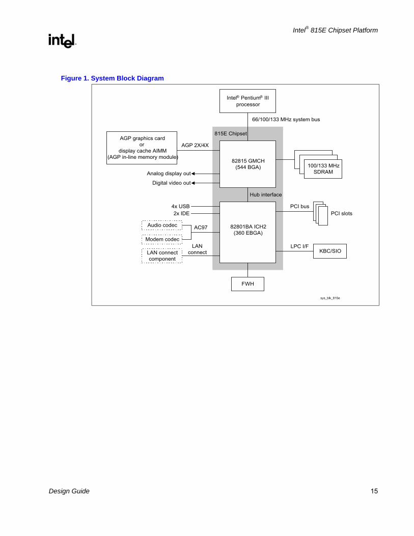
1.2. System Overview The Intel 815E chipset contains a Graphics Memory Controller Hub (GMCH) component and I/O Controller Hub 2 (ICH2) component for desktop platforms.
The GMCH provides the processor interface (optimized for the Intel PentiumIII processors and Intel
Celeron™ processors), DRAM interface, hub interface, and an AGP interface or internal graphics.This product provides flexibility and scalability in graphics and memory subsystem performance. Competitive internal graphics may be scaled via an AGP card interface and PC100 SDRAM system memory may be scaled to PC133 system memory.
The Accelerated Hub Architecture interface (i.e., the chipset component interconnect) is designed into the chipset to provide an efficient, high-bandwidth communication channel between the Intel® 815E chipset’s graphics and memory controller hub and the I/O hub controller. The chipset architecture also enables a security and manageability infrastructure through the Firmware Hub component.
An ACPI-compliant Intel® 815E chipset platform can support the Full-on (S0), Stop Grant (S1), Suspend to RAM (S3), Suspend to Disk (S4), and Soft-off (S5) power management states. The chipset also supports wake-on-LAN* for remote administration and troubleshooting. The chipset architecture removes the requirement for the ISA expansion bus that was traditionally integrated into the I/O subsystem of PCIsets/AGPsets. This removes many of the conflicts experienced when installing hardware and drivers into legacy ISA systems. The elimination of ISA provides true plug-and-play for the platform. Traditionally, the ISA interface was used for audio and modem devices. The addition of AC’97 allows the OEM to use software-configurable AC’97 audio and modem coder/decoders (codecs), instead of the traditional ISA devices.
1.2.1. System Features
The Intel® 815E chipset contains twocomponents: the 82815 Graphics and Memory Controller Hub (GMCH) and the 82801BA I/O Controller Hub 2 (ICH2). The GMCH integrates a 66/100/133-MHz, P6 family system bus controller, integrated 2D/3D graphics accelerator or AGP (2X/4X) discrete graphics card, 100/133-MHz SDRAM controller, and a high-speed accelerated hub architecture interface for communication with the ICH2. The ICH2 integrates an UltraATA/100 controller, 2 USB host controllers with a total of 4 ports, LPC interface controller, FWH interface controller, PCI interface controller, AC’97 digital link, integrated LAN controller, and a hub interface for communication with the GMCH.
Intel® 815E Chipset Platform
R
Design Guide 15
Figure 1. System Block Diagram
sys_blk_815e
Intel® Pentium® IIIprocessor
82815 GMCH(544 BGA)
82801BA ICH2(360 EBGA)
KBC/SIO
AGP graphics cardor
display cache AIMM(AGP in-line memory module)
AGP 2X/4X
Analog display out
Digital video out
66/100/133 MHz system bus
Hub interface
100/133 MHzSDRAM
PCI slots
FWH
4x USB2x IDE
Audio codec
Modem codec
AC97
LAN connectcomponent
LPC I/F
PCI bus
LANconnect
815E Chipset
Intel® 815E Chipset Platform
R
16 Design Guide
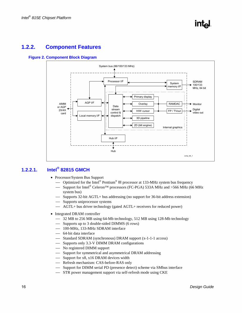
1.2.2. Component Features Figure 2. Component Block Diagram
System bus (66/100/133 MHz)
Processor I/FSystem
memory I/F
AGP I/F
Local memory I/F
Hub I/F
Datastream
control &dispatch
Primary display
Overlay
H/W cursor
3D pipeline
2D (blit engine)
RAMDAC
FP / TVout
Internal graphics
AIMMor AGP2X/4X
card
Hub
SDRAM100/133MHz, 64 bit
Monitor
Digitalvideo out
comp_blk_1
1.2.2.1. Intel® 82815 GMCH • Processor/System Bus Support
Optimized for the Intel® Pentium® III processor at 133-MHz system bus frequency Support for Intel® Celeron™ processors (FC-PGA) 533A MHz and >566 MHz (66 MHz
system bus) Supports 32-bit AGTL+ bus addressing (no support for 36-bit address extension) Supports uniprocessor systems AGTL+ bus driver technology (gated AGTL+ receivers for reduced power)
• Integrated DRAM controller 32 MB to 256 MB using 64-Mb technology, 512 MB using 128-Mb technology Supports up to 3 double-sided DIMMS (6 rows) 100-MHz, 133-MHz SDRAM interface 64-bit data interface Standard SDRAM (synchronous) DRAM support (x-1-1-1 access) Supports only 3.3-V DIMM DRAM configurations No registered DIMM support Support for symmetrical and asymmetrical DRAM addressing Support for x8, x16 DRAM devices width Refresh mechanism: CAS-before-RAS only Support for DIMM serial PD (presence detect) scheme via SMbus interface STR power management support via self-refresh mode using CKE

Intel® 815E Chipset Platform
R
Design Guide 17
• Accelerated Graphics Port (AGP) Interface Supports AGP 2.0, including 4X AGP data transfers, but not the 2X/4X Fast Write protocol AGP universal connector support via dual-mode buffers to allow AGP 2.0 3.3-V or 1.5-V
signaling 32-deep AGP request queue AGP address translation mechanism with integrated fully associative 20-entry TLB High-priority access support Delayed transaction support for AGP reads that can not be serviced immediately AGP semantic traffic to the DRAM is not snooped on the system bus and is therefore not
coherent with the processor caches.
• Integrated Graphics Controller Full 2D/3D/DirectX acceleration Texture-mapped 3D with point sampled, bilinear, trilinear, and anisotropic filtering Hardware setup with support for strips and fans Hardware motion compensation assist for software MPEG/DVD decode Digital Video Out interface adds support for digital displays and TV-Out. PC9X compliant Integrated 230-MHz DAC
• Integrated Local Graphics Memory Controller (Display Cache) 0 MB to 4 MB (via AIMM) using zero, one or two parts 32-bit data interface 133-MHz memory clock Supports ONLY 3.3-V SDRAMs
• Packaging/Power 544 BGA with local memory port 1.85-V (± 3% within margins of 1.795 V to 1.9 V) core and mixed 3.3-V, 1.5-V and AGTL+
I/O

Intel® 815E Chipset Platform
R
18 Design Guide
1.2.2.2. Intel® 82801BA I/O Controller Hub 2 (ICH2)
The I/O Controller Hub 2 allows the I/O subsystem to access the rest of the system, as follows:
• Upstream accelerated hub architecture interface for access to the GMCH
• PCI 2.2 interface (6 PCI Req/Grant pairs)
• Bus master IDE controller: supports Ultra ATA/100
• USB controller
• I/O APIC
• SMBus controller
• FWH interface
• LPC interface
• AC’97 2.1 interface
• Integrated system management controller
• Alert-on-LAN*
• Integrated LAN controller
• Packaging / power 360 EBGA 1.8-V core and 3.3-V standby
1.2.2.3. Firmware Hub (FWH)
The hardware features of this device include:
• An integrated hardware Random Number Generator (RNG)
• Register-based locking
• Hardware-based locking
• 5 GPIs
• Packaging/Power 40L TSOP and 32L PLCC 3.3-V core and 3.3 V / 12 V for fast programming

Intel® 815E Chipset Platform
R
Design Guide 19
1.2.3. Platform Initiatives
1.2.3.1. Intel® PC 133
Intel PC133 initiative provides the memory bandwidth necessary to obtain high performance from the Intel® Pentium® III processor and AGP graphics controllers. The Intel® 815E chipset’s SDRAM interface supports 100-MHz and 133-MHz operation. The latter delivers 1.066 GB/s of theoretical memory bandwidth compared with the 800-MB/s theoretical memory bandwidth of 100-MHz SDRAM systems.
1.2.3.2. Accelerated Hub Architecture Interface
As I/O speeds increase, the demand placed on the PCI bus by the I/O bridge becomes significant. With the addition of AC’97 and Ultra ATA/100, coupled with the existing USB, I/O requirements could impact PCI bus performance. The Intel 815E chipset’s accelerated hub architecture ensures that the I/O subsystem, both PCI and the integrated I/O features (IDE, AC’97, USB, LAN), receives adequate bandwidth. By placing the I/O bridge on the accelerated hub architecture interface instead of PCI, I/O functions integrated into the ICH2 and the PCI peripherals are ensured the bandwidth necessary for peak performance.
1.2.3.3. Internet Streaming SIMD Extensions
The Intel PentiumIII processor provides 70 new SIMD (single instruction, multiple data) instructions. The new extensions are floating-point SIMD Extensions. Intel MMX™ technology provides integer SIMD instructions. The Internet Streaming SIMD extensions complement the Intel MMX technology SIMD instructions and provide a performance boost to floating-point-intensive 3D applications.
1.2.3.4. AGP 2.0
The AGP 2.0 interface allows graphics controllers to access main memory at over 1 GB/s, twice the bandwidth of previous AGP platforms. AGP 2.0 provides the infrastructure necessary for photorealistic 3D. In conjunction with the Internet Streaming SIMD Extensions, AGP 2.0 delivers the next level of 3D graphics performance.
1.2.3.5. Integrated LAN Controller
The Intel® 815E chipset platform incorporates an ICH2 integrated LAN Controller. Its bus master capabilities enable the component to process high-level commands and perform multiple operations; this lowers processor utilization by off-loading communication tasks from the processor.
The ICH2 functions with several options of LAN connect components to target the desired market segment. The 82562EH provides a HomePNA 1-Mbit/sec connection. The 82562ET provides a basic Ethernet 10/100 connection. The 82562EM provides an Ethernet 10/100 connection with the added flexibility of Alert on LAN.
Intel® 815E Chipset Platform
R
20 Design Guide
1.2.3.6. Ultra ATA/100 Support
The Intel® 815E chipset platform incorporates the ICH2 IDE controller with two sets of interface signals (primary and secondary) that can be independently enabled, tri-stated or driven low. The platform supports Ultra ATA/100 for transfers up to 100MB/sec, in addition to Ultra ATA/66, and Ultra ATA/33 modes.
1.2.3.7. Expanded USB Support
The Intel® 815E chipset platform contains two USB Host Controllers. Each Host Controller includes a root hub with two separate USB ports each, for a total of 4 USB ports. The addition of a second USB Host Controller expands the functionality of the platform.
1.2.3.8. Manageability and Other Enhancements
The Intel® 815E chipset platform integrates several functions designed to manage the system and lower the total cost of ownership (TCO) of the system. The platform supports all features in the Intel® 815E chipset, in addition to the following features. These system management functions are designed to report errors, diagnose the system, and recover from system lockups, without the aid of an external microcontroller.
SMBus
The ICH2 integrates a SMBus controller. The SMBus provides an interface for managing peripherals such as serial presence detection (SPD) and thermal sensors. The slave interface allows an external microcontroller to access system resources.
Interrupt Controller
The interrupt capabilities of the Intel® 815E chipset platform expand support for up to 8 PCI interrupt pins and PCI 2.2 message-based interrupts. In addition, the ICH2 supports system bus interrupt delivery.
Firmware Hub (FWH)
The Intel® 815E chipset platform supports firmware hub BIOS memory sizes up to 8 MB for increased system flexibility.

Intel® 815E Chipset Platform
R
Design Guide 21
1.2.3.9. AC’97 6-Channel Support
The Audio Codec ’97 (AC’97) Specification defines a digital interface that can be used to attach an audio codec (AC), a modem codec (MC), an audio/modem codec (AMC), or both an AC and a MC. The AC’97 Specification defines the interface between the system logic and the audio or modem codec known as the AC’97 Digital Link.
The Intel® 815E chipset’s AC’97 (with the appropriate codecs) not only replaces ISA audio and modem functionality, but also improves overall platform integration by incorporating the AC’97 digital link. Using Intel® 815E chipset’s integrated AC’97 digital link reduces cost and eases migration from ISA.
By using an audio codec, the AC’97 digital link allows for cost-effective, high-quality, integrated audio on the Intel® 815E chipset platform. In addition, an AC’97 soft modem can be implemented with the use of a modem codec. Several system options exist when implementing AC’97. The Intel® 815E chipset’s integrated digital link allows several external codecs to be connected to the ICH2. The system designer can provide audio with an audio codec, a modem with a modem codec, or an integrated audio/modem codec (Figure 3c). The digital link is expanded to support two audio codecs (Figure 3a) or a combination of an audio and modem codec (Figure 3b).
Modem implementation for different countries must be taken into consideration, as telephone systems may vary. By implementing a split design, the audio codec can be on board and the modem codec can be placed on a riser. Intel is developing a Communications and Networking Riser connector.
The digital link in the ICH2 is AC’97 Rev. 2.1 compliant, supporting two codecs with independent PCI functions for audio and modem. Microphone input and left and right audio channels are supported for a high-quality, two-speaker audio solution. Wake-on-ring-from-suspend also is supported with the appropriate modem codec.
The Intel® 815E chipset platform expands audio capability with support for up to six channels of PCM audio output (i.e., full AC3 decode). Six-channel audio consists of Front Left, Front Right, Back Left, Back Right, Center and Woofer, for a complete surround sound effect. ICH2 has expanded support for two audio codecs on the AC’97 digital link.

Intel® 815E Chipset Platform
R
22 Design Guide
Figure 3. AC'97 Audio and Modem Connections
AC97_connections
ICH2360 EBGA
AC97ModemCODEC
Modem Port
Audio Port
AC97 DigitalLink
AC97Audio/
CODEC
ICH2360 EBGA
AC97AudioCodecAC97 Digital
Link
AC97AudioCodec
Audio Port
Audio Port
ICH2360 EBGA
AC97 DigitalLink AC97
Audio/ModemCodec
Audio Port
Modem Port
a) AC'97 with Audio Codecs (4-Channel Secondary)
b) AC'97 with Modem and Audio Codecs
c) AC'97 with Audio/Modem Codec

Intel® 815E Chipset Platform
R
Design Guide 23
1.2.3.10. Low-Pin-Count (LPC) Interface
In the Intel® 815E chipset platform, the Super I/O (SIO) component has migrated to the Low-Pin-Count (LPC) interface. Migration to the LPC interface allows for lower-cost Super I/O designs. The LPC Super I/O component requires the same feature set as traditional Super I/O components. It should include a keyboard and mouse controller, floppy disk controller, and serial and parallel ports. In addition to the Super I/O features, an integrated game port is recommended because the AC’97 interface does not provide support for a game port. In systems with ISA audio, the game port typically existed on the audio card. The fifteen-pin game port connector provides for two joysticks and a two-wire MPU-401 MIDI interface. Consult your preferred Super I/O vendor for a comprehensive list of the devices offered and the features supported.
In addition, depending on system requirements, specific system I/O requirements may be integrated into the LPC Super I/O. For example, a USB hub may be integrated to connect to the ICH2 USB output and extend it to multiple USB connectors. Other SIO integration targets include a device bay controller or an ISA-IRQ-to-serial-IRQ converter to support a PCI-to-ISA bridge. Contact your Super I/O vendor to ensure the availability of desired LPC Super I/O features.
1.2.3.11. Security – The Intel Random Number Generator
The Intel® 815E chipset based system contains the first of Intel’s platform security features, the Intel Random Number Generator (RNG). The Intel RNG is a component of the 82802 Firmware Hub (FWH), and it supplies applications and security middleware products with true non-deterministic random numbers, through the Intel Security Driver.
Better random numbers lead to better security. Most cryptographic functions, especially functions that provide authentication or encryption services, require random numbers for such purposes as key generation. One attack on those cryptographic functions is to predict the random numbers being used to generate those keys. Current methods that use system and user input to seed a pseudo-random number generator have proved vulnerable to such attacks. The RNG uses thermal noise across a resistor to generate true non-deterministic, unpredictable random numbers.
Applications often access cryptographic functions through security middleware products such as Microsoft's CAPI*, RSA's BSAFE*, and the OpenGroup's CDSA*. Intel is working to ensure that middleware products and applications are enabled to take advantage of this capability. By implementing the BIOS requirements and testing and loading the Intel Security Driver, it is possible to ensure that the Intel RNG is enabled for a platform design.

Intel® 815E Chipset Platform
R
24 Design Guide
The ICH2BIOS Specification contains complete details regarding BIOS requirements for enabling the RNG. In summary, the system BIOS must contain a System Device Node for the FWH device for plug-and-play operating systems (OS) to use the Random Number Generator through the Security Driver. The devnode is required for the OS to find the FWH at enumeration time, and the specific devnode number associates the FWH with the Security Driver.
• The BIOS must report a single device node for the FWH.
• Intel-specific EISA ID (devnode number must be INT0800)
• Device type: System peripherals / other
• Device attrib: Non-configurable and cannot be disabled
• ANSI ID string: “Intel FWH”
• Memory range descriptor: Describing feature space
• For PnP OSes, BIOS ranges are allocated through E820h and ACPI structures, as in current BIOSes.
• For non-PnP OSes, FWH ranges should be reserved through the Int 15h E820h function.
A complete Intel® 815E chipset-based system must have the Security Driver loaded for applications to take advantage of the Random Number Generator. The Security Driver implements an interface that middleware and some applications call to access the RNG. The Security Driver can be obtained from the PCG Chipset Driver download website at http://developer.intel.com/design/chipsets/drivers/SWDev/.

Intel® 815E Chipset Platform
R
Design Guide 25
2. General Design Considerations This section documents motherboard layout and routing guidelines for Intel 815E chipset-based systems. This section does not discuss the functional aspects of any bus or the layout guidelines for an add-in device.
If the guidelines listed in this document are not followed, it is very important that thorough signal integrity and timing simulations be completed for each design. Even when the guidelines are followed, critical signals should be simulated to ensure the proper signal integrity and flight time. Any deviation from these guidelines should be simulated.
The trace impedance typically noted (i.e., 60 Ω ± 15%) is the “nominal” trace impedance for a 5-mil-wide trace. That is, it is the impedance of the trace when not subjected to the fields created by changing current in neighboring traces. When calculating flight times, it is important to consider the minimum and maximum impedance of a trace, based on the switching of neighboring traces. The use of wider spaces between the traces can minimize this trace-to-trace coupling. In addition, these wider spaces reduce the settling time.
Coupling between two traces is a function of the coupled length, the distance separating the traces, the signal edge rate, and the degree of mutual capacitance and inductance. To minimize the effects of trace-to-trace coupling, the routing guidelines documented in this section should be followed.
Additionally, these routing guidelines are created using a PCB stack-up similar to that illustrated in the following figure.
2.1. Nominal Board Stack-up The Intel® 815E chipset platform requires a board stack-up yielding a target impedance of 60 Ω ± 15% with a 5-mil nominal trace width. The following figure presents an example stack-up that achieves this. It is a 4-layer printed circuit board (PCB) construction using 53%-resin FR4 material.
Figure 4. Board Construction Example for 60-ΩΩΩΩ Nominal Stack-up
board_4.5mil_stackup
~48-mil core
Component-side layer 1: ½ oz. Cu
Power plane layer 2: 1 oz. Cu4.5-mil prepreg
Ground layer 3: 1 oz. Cu
Solder-side layer 4: ½ oz. Cu4.5-mil prepreg
Total thickness:62 mils

Intel® 815E Chipset Platform
R
26 Design Guide
This page intentionally left blank.
Intel® 815E Chipset Platform
R
Design Guide 27
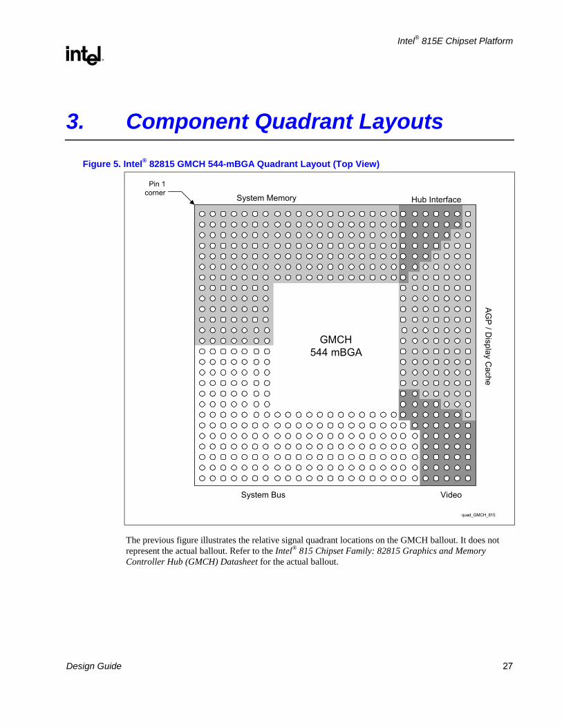
3. Component Quadrant Layouts
Figure 5. Intel® 82815 GMCH 544-mBGA Quadrant Layout (Top View)
quad_GMCH_815
GMCH544 mBGA
System Memory
AGP / D
isplay Cache
Video
Hub Interface
System Bus
Pin 1corner
The previous figure illustrates the relative signal quadrant locations on the GMCH ballout. It does not represent the actual ballout. Refer to the Intel® 815 Chipset Family: 82815 Graphics and Memory Controller Hub (GMCH) Datasheet for the actual ballout.

Intel® 815E Chipset Platform
R
28 Design Guide
Figure 6. ICH2 Quadrant Layout (Top View)
IDE
SM busAC'97
LAN
Hub interface Processor
PCI LPC USB
ICH2360 EBGA
quad_ICH2
The diagram in the previous figure illustrates the relative signal quadrant locations on the ICH2 ballout. It does not represent the actual ballout. Refer to the Intel® 82801BA I/O Controller Hub 2 (ICH2) Datasheet for the actual ballout.

Intel® 815E Chipset Platform
R
Design Guide 29
Figure 7. Firmware Hub (FWH) Packages
pck_fwh.vsd
1234567891011121314151617181920
4039383736353433323130292827262524232221
FWH Interface
(40-Lead TSOP)
5
6
7
8
9
10
11
12
13
29
28
27
26
25
24
23
22
21
1234 32 31 30
14 15 16 17 18 19 20
FWH Interface
(32-Lead PLCC,0.450" x 0.550")
Top View

Intel® 815E Chipset Platform
R
30 Design Guide
This page is intentionally left blank.

Intel® 815E Chipset Platform
R
Design Guide 31
4. System Bus Design Guidelines
4.1. Introduction The newest generation of the Intel® Pentium® III processor delivers higher performance by integrating the Level 2 cache into the processor and running it at the processor's core speed. The Intel® Pentium® III processor runs at a higher core and system bus speeds than previous-generation IA-32 processors, while maintaining hardware and software compatibility with earlier Intel® Pentium® III processors. New Flip Chip-Pin Grid Array (FC-PGA) package technology enables compatibility with the PGA370 socket.
This section presents the design considerations for flexible platforms capable of using the Intel® 815E chipset with the full range of Intel® Pentium® III processors using the PGA370 socket.
4.1.1. Terminology
For this document, the following terminology applies:
• Flexible PGA370 refers to new-generation Intel® 815E chipsets using the new, “flexible” PGA370 socket. In general, these designs support 100/133-MHz system bus operation, VRM 8.4 DC-DC converter guidelines, and the Intel® Pentium® III processor (FC-PGA) in single-microprocessor based designs.
Note: The system bus speed supported by the design is based on the capabilities of the used processor, chipset, and clock driver.
4.2. System Bus Routing Guidelines The following layout guide supports designs using Intel® Pentium III processors with the Intel 815E chipset. The solution covers system bus speeds of 100/133 MHz for Intel® Pentium III processors. The solution proposed in this section requires the motherboard design to terminate the system bus AGTL+ signals with 56 Ω ±5% Rtt resistors. Intel® Pentium III processors in FC-PGA must also be configured to 110-Ω internal Rtt resistors.
4.2.1. Initial Timing Analysis
The following table lists the AGTL+ component timings of the processors and Intel 815E chipset’s GMCH defined at the pins. These timings are for reference only. Obtain each processor’s specifications from its respective processor electrical, mechanical, and thermal specification and the appropriate Intel 815E chipset component specification.
Intel® 815E Chipset Platform
R
32 Design Guide
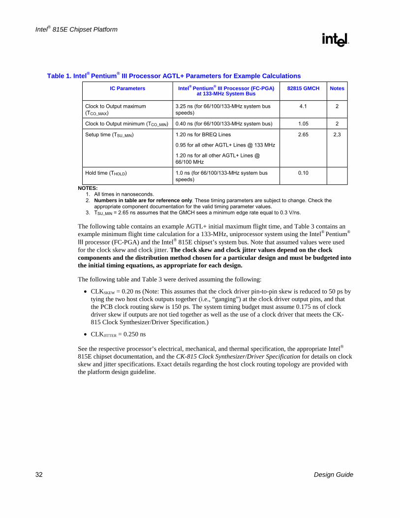
Table 1. Intel® Pentium® III Processor AGTL+ Parameters for Example Calculations
IC Parameters Intel® Pentium® III Processor (FC-PGA) at 133-MHz System Bus
82815 GMCH Notes
Clock to Output maximum (TCO_MAX)
3.25 ns (for 66/100/133-MHz system bus speeds)
4.1 2
Clock to Output minimum (TCO_MIN) 0.40 ns (for 66/100/133-MHz system bus) 1.05 2
Setup time (TSU_MIN) 1.20 ns for BREQ Lines
0.95 for all other AGTL+ Lines @ 133 MHz
1.20 ns for all other AGTL+ Lines @ 66/100 MHz
2.65 2,3
Hold time (THOLD) 1.0 ns (for 66/100/133-MHz system bus speeds)
0.10
NOTES: 1. All times in nanoseconds. 2. Numbers in table are for reference only. These timing parameters are subject to change. Check the
appropriate component documentation for the valid timing parameter values. 3. TSU_MIN = 2.65 ns assumes that the GMCH sees a minimum edge rate equal to 0.3 V/ns.
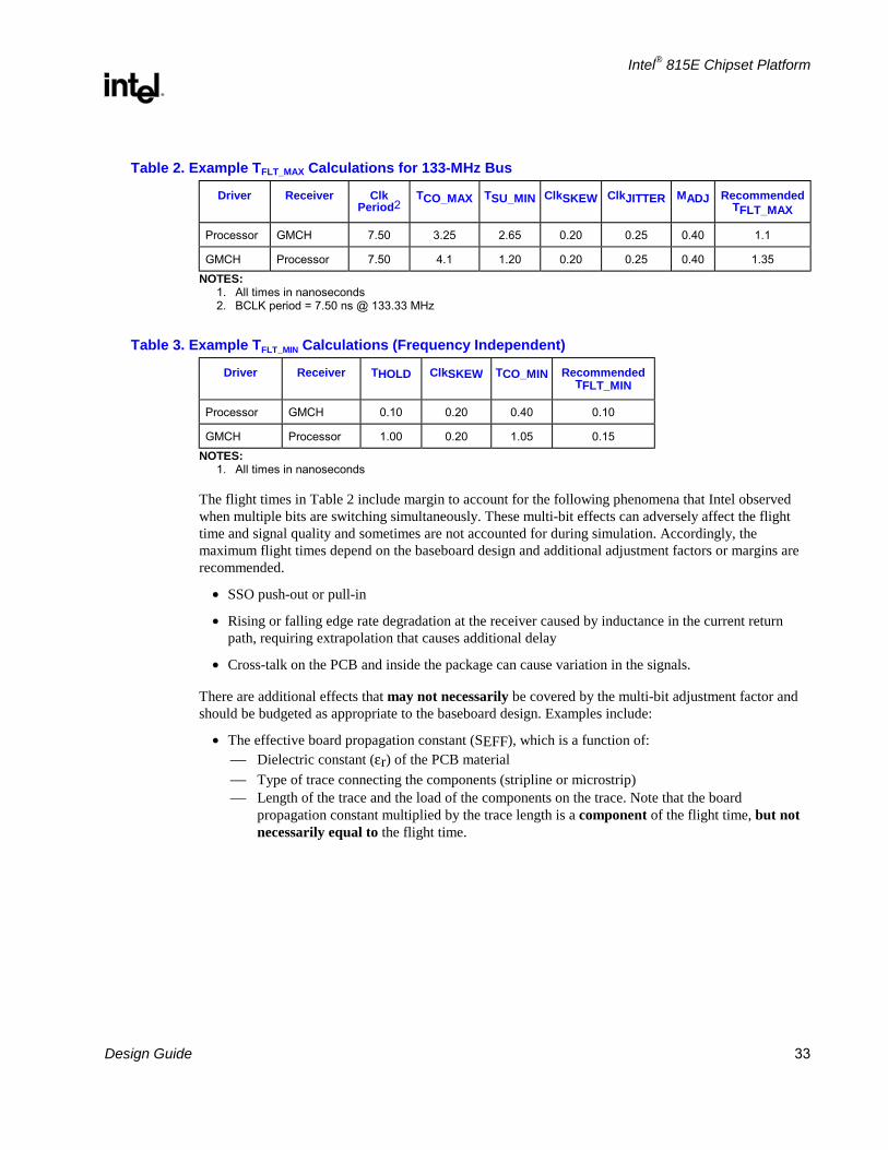
The following table contains an example AGTL+ initial maximum flight time, and Table 3 contains an example minimum flight time calculation for a 133-MHz, uniprocessor system using the Intel® Pentium® III processor (FC-PGA) and the Intel 815E chipset’s system bus. Note that assumed values were used for the clock skew and clock jitter. The clock skew and clock jitter values depend on the clock components and the distribution method chosen for a particular design and must be budgeted into the initial timing equations, as appropriate for each design.
The following table and Table 3 were derived assuming the following:
• CLKSKEW = 0.20 ns (Note: This assumes that the clock driver pin-to-pin skew is reduced to 50 ps by tying the two host clock outputs together (i.e., “ganging”) at the clock driver output pins, and that the PCB clock routing skew is 150 ps. The system timing budget must assume 0.175 ns of clock driver skew if outputs are not tied together as well as the use of a clock driver that meets the CK-815 Clock Synthesizer/Driver Specification.)
• CLKJITTER = 0.250 ns
See the respective processor’s electrical, mechanical, and thermal specification, the appropriate Intel 815E chipset documentation, and the CK-815 Clock Synthesizer/Driver Specification for details on clock skew and jitter specifications. Exact details regarding the host clock routing topology are provided with the platform design guideline.
Intel® 815E Chipset Platform
R
Design Guide 33
Table 2. Example TFLT_MAX Calculations for 133-MHz Bus
Driver Receiver Clk Period2
TCO_MAX TSU_MIN ClkSKEW ClkJITTER MADJ Recommended TFLT_MAX
Processor GMCH 7.50 3.25 2.65 0.20 0.25 0.40 1.1
GMCH Processor 7.50 4.1 1.20 0.20 0.25 0.40 1.35 NOTES:
1. All times in nanoseconds 2. BCLK period = 7.50 ns @ 133.33 MHz
Table 3. Example TFLT_MIN Calculations (Frequency Independent)
Driver Receiver THOLD ClkSKEW TCO_MIN Recommended TFLT_MIN
Processor GMCH 0.10 0.20 0.40 0.10
GMCH Processor 1.00 0.20 1.05 0.15 NOTES:
1. All times in nanoseconds
The flight times in Table 2 include margin to account for the following phenomena that Intel observed when multiple bits are switching simultaneously. These multi-bit effects can adversely affect the flight time and signal quality and sometimes are not accounted for during simulation. Accordingly, the maximum flight times depend on the baseboard design and additional adjustment factors or margins are recommended.
• SSO push-out or pull-in
• Rising or falling edge rate degradation at the receiver caused by inductance in the current return path, requiring extrapolation that causes additional delay
• Cross-talk on the PCB and inside the package can cause variation in the signals.
There are additional effects that may not necessarily be covered by the multi-bit adjustment factor and should be budgeted as appropriate to the baseboard design. Examples include:
• The effective board propagation constant (SEFF), which is a function of: Dielectric constant (εr) of the PCB material Type of trace connecting the components (stripline or microstrip) Length of the trace and the load of the components on the trace. Note that the board
propagation constant multiplied by the trace length is a component of the flight time, but not necessarily equal to the flight time.

Intel® 815E Chipset Platform
R
34 Design Guide
4.3. General Topology and Layout Guidelines The following topology and layout guidelines are preliminary and subject to change. The guidelines are derived from empirical testing with the Intel® 810E chipset as well as correlative simulations with preliminary Intel® 815E chipset package models. Refer to the Intel® Celeron™ processor datasheet and the Intel® Pentium® III processor for the PGA370 socket datasheet for detailed information on processor signal groups and pin definitions.
In the Single-Ended Termination (SET) topology for the 370-pin socket (PGA370), the termination should be placed close to the processor on the motherboard. There is no termination present at the chipset end of the network. Due to the lack of termination, SET will exhibit much more ringback than the dual-terminated topology. Extra care will be required in SET simulations to make sure that the ringback specs are met under the worst-case signal quality conditions. Intel 815E chipset designs require all AGTL+ signals to be terminated with a 56-Ω termination on the motherboard. To ensure processor signal integrity requirements, it is highly recommended that all system bus signal segments be referenced to the ground plane for the entire route.
Figure 8. Topology for 370-Pin Socket Designs with Single-Ended Termination (SET)
sys_bus_topo_PGA370
GMCHPGA370Socket
L(1): Z0 = 60 Ω ± 15%
Vtt
56 Ω
L2L3L1
Table 4. Segment Descriptions and Lengths for Figure 8
Segment Description Min. Length (inches) Max. Length (inches)
L1+L2 GMCH to Rtt stub 1.90 4.50
L2 PGA370 pin to Rtt stub 0.0 0.20
L3 Rtt stub length 0.50 2.50 NOTES:
1. All AGTL+ bus signals should be referenced to the ground plane for the entire route.
Intel® 815E Chipset Platform
R
Design Guide 35
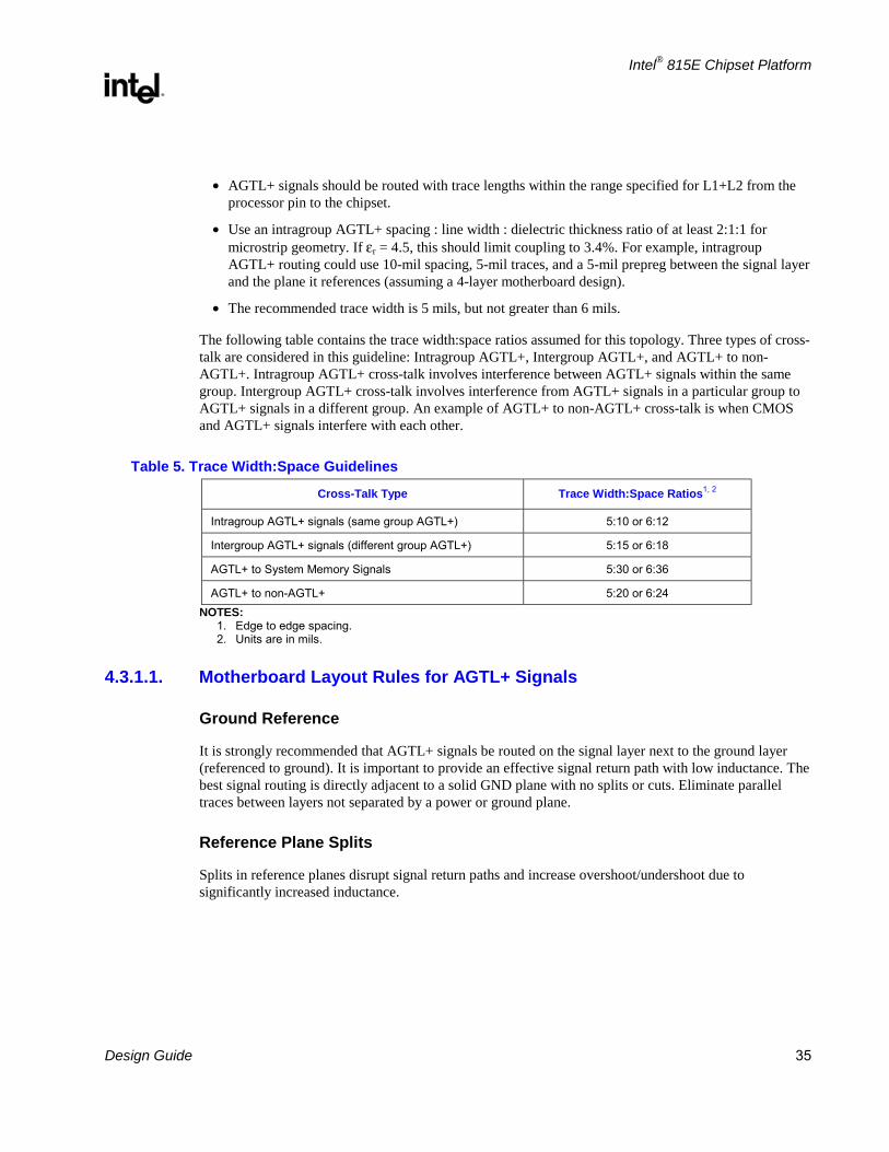
• AGTL+ signals should be routed with trace lengths within the range specified for L1+L2 from the processor pin to the chipset.
• Use an intragroup AGTL+ spacing : line width : dielectric thickness ratio of at least 2:1:1 for microstrip geometry. If εr = 4.5, this should limit coupling to 3.4%. For example, intragroup AGTL+ routing could use 10-mil spacing, 5-mil traces, and a 5-mil prepreg between the signal layer and the plane it references (assuming a 4-layer motherboard design).
• The recommended trace width is 5 mils, but not greater than 6 mils.
The following table contains the trace width:space ratios assumed for this topology. Three types of cross-talk are considered in this guideline: Intragroup AGTL+, Intergroup AGTL+, and AGTL+ to non-AGTL+. Intragroup AGTL+ cross-talk involves interference between AGTL+ signals within the same group. Intergroup AGTL+ cross-talk involves interference from AGTL+ signals in a particular group to AGTL+ signals in a different group. An example of AGTL+ to non-AGTL+ cross-talk is when CMOS and AGTL+ signals interfere with each other.
Table 5. Trace Width:Space Guidelines
Cross-Talk Type Trace Width:Space Ratios1, 2
Intragroup AGTL+ signals (same group AGTL+) 5:10 or 6:12
Intergroup AGTL+ signals (different group AGTL+) 5:15 or 6:18
AGTL+ to System Memory Signals 5:30 or 6:36
AGTL+ to non-AGTL+ 5:20 or 6:24 NOTES:
1. Edge to edge spacing. 2. Units are in mils.
4.3.1.1. Motherboard Layout Rules for AGTL+ Signals
Ground Reference
It is strongly recommended that AGTL+ signals be routed on the signal layer next to the ground layer (referenced to ground). It is important to provide an effective signal return path with low inductance. The best signal routing is directly adjacent to a solid GND plane with no splits or cuts. Eliminate parallel traces between layers not separated by a power or ground plane.
Reference Plane Splits
Splits in reference planes disrupt signal return paths and increase overshoot/undershoot due to significantly increased inductance.

Intel® 815E Chipset Platform
R
36 Design Guide
Processor Connector Breakout
It is strongly recommended that AGTL+ signals do not traverse multiple signal layers. Intel recommends breaking out all signals from the connector on the same layer. If routing is tight, break out from the connector on the opposite routing layer over a ground reference and cross over to main signal layer near the processor connector.
Note: Following the previously mentioned layout rules is critical for AGTL+ signal integrity, particularly for the 0.18-micron process technology.
Minimizing Cross-Talk
The following general rules minimize the impact of cross-talk in a high-speed AGTL+ bus design:
• Maximize the space between traces. Wherever possible, maintain a minimum of 10 mils (assuming a 5-mil trace) between trace edges. It may be necessary to use tighter spacing when routing between component pins. When traces must be close and parallel to each other, minimize the distance that they are close together and maximize the distance between the sections when the spacing restrictions are relaxed.
• Avoid parallelism between signals on adjacent layers, if there is no AC reference plane between them. As a rule of thumb, route adjacent layers orthogonally.
• Since AGTL+ is a low-signal-swing technology, it is important to isolate AGTL+ signals from other signals by at least 25 mils. This will avoid coupling from signals that have larger voltage swings, such as 5-V PCI.
• AGTL+ signals must be well isolated from system memory signals. AGTL+ signal trace edges must be at least 30 mils from system memory trace edges within 100 mils of the ball of the Intel® 82815 GMCH.
• Select a board stack-up that minimizes the coupling between adjacent signals. Minimize the nominal characteristic impedance within the AGTL+ specification. This can be done by minimizing the height of the trace from its reference plane, which minimizes cross-talk.
• Route AGTL+ address, data, and control signals in separate groups to minimize cross-talk between groups. Keep at least 25 mils between each group of signals.
• Minimize the dielectric used in the system. This makes the traces closer to their reference plane and thus reduces the cross-talk magnitude.
• Minimize the dielectric process variation used in the PCB fabrication.
• Minimize the cross-sectional area of the traces. This can be done by means of narrower traces and/or by using thinner copper, but the trade-off for this smaller cross-sectional area is higher trace resistivity, which can reduce the falling-edge noise margin because of the I*R loss along the trace.

Intel® 815E Chipset Platform
R
Design Guide 37
4.3.1.2. Motherboard Layout Rules for Non-AGTL+ (CMOS) Signals
Table 6. Routing Guidelines for Non-AGTL+ Signals
Signal Trace Width Spacing to Other Traces Trace Length
A20M# 5 mils 10 mils 1 to 9
FERR# 5 mils 10 mils 1 to 9
FLUSH# 5 mils 10 mils 1 to 9
IERR# 5 mils 10 mils 1 to 9
IGNNE# 5 mils 10 mils 1 to 9
INIT# 5 mils 10 mils 1 to 9
LINT[0] (INTR) 5 mils 10 mils 1 to 9
LINT[1] (NMI) 5 mils 10 mils 1 to 9
PICD[1:0] 5 mils 10 mils 1 to 9
PREQ# 5 mils 10 mils 1 to 9
PWRGOOD 5 mils 10 mils 1 to 9
SLP# 5 mils 10 mils 1 to 9
SMI# 5 mils 10 mils 1 to 9
STPCLK 5 mils 10 mils 1 to 9
THERMTRIP# 5 mils 10 mils 1 to 9 NOTES:
1. Route these signals on any layer or combination of layers.
4.3.1.3. THRMDP and THRMDN
These traces (THRMDP and THRMDN) route the processor’s thermal diode connections. The thermal diode operates at very low currents and may be susceptible to cross-talk. The traces should be routed close together to reduce loop area and inductance.
Figure 9. Routing for THRMDP and THRMDN
1 Maximize (min. 20 mils)
1 Maximize (min. 20 mils)
2 Minimize
Signal Y
THRMDP
THERMDN
Signal Z
bus_routing_thrmdp-thrmdn NOTES:
1. Route these traces parallel and equalize lengths within ±0.5. 2. Route THRMDP and THRMDN on the same layer

Intel® 815E Chipset Platform
R
38 Design Guide
4.3.1.4. Additional Routing and Placement Considerations • Distribute VTT with a wide trace. A 0.050” minimum trace is recommended to minimize DC losses.
Route the VTT trace to all components on the host bus. Be sure to include decoupling capacitors.
• The VTT voltage should be 1.5 V ± 3% for static conditions, and 1.5 V ± 9% for worst-case transient conditions.
• Place resistor divider pairs for VREF generation at the GMCH component. VREF also is delivered to the processor.
4.3.2. GTLREF Topology and Layout for Debug
It is strongly recommended that resistor sites be added to the layout to split the GTLREF sources to the processor and the chipset. This will allow the designer to independently modify the reference voltage to each component for debug purposes. The recommended GTLREF circuit topology is shown the figure below.
Figure 10. GTLREF Circuit Topology
gtlref_circuit
VTT
R4 (No-Pop)75 Ω
R175 Ω
R30 Ω
R5 (No-Pop)150 Ω
R2150 Ω
ProcessorGMCH
• Normal shared GTLREF (one source, routed to both the GMCH and CPU) Populate R1, R2, and R3 with values shown Do NOT Populate R4 and R5
• Independent GTLREF for Platform Debug (independent sources for each the GMCH and processor) Populate R1, R2, R4, and R5 with values shown Do NOT Populate R3
GTLREF Layout and Routing Guidelines • Place all resistor sites for GTLREF generation close to the GMCH.
• Route GTLREF with as wide a trace as possible.
• Use 1-0.1uF decoupling capacitor for every 2 GTLREF pins at the CPU (4 capacitors total). Place as close as possible (within 500mils) to the Socket 370 GTLREF pins.
• Use 1-0.1uF decoupling capacitor for each of the 2 GTLREF pins at the GMCH (2 capacitors total). Place as close as possible to the GMCH GTLREF balls.

Intel® 815E Chipset Platform
R
Design Guide 39
4.4. Electrical Differences for Flexible PGA370 Designs There are several electrical changes between the legacy PGA370 and flexible PGA370 design, as follows:
• Changes to the PGA370 socket pin definitions. Intel® Pentium® III processors (FC-PGA) utilize a superset of the Intel® Celeron™ processor (PPGA) pin definition.
• Addition of VTT (AGTL+ termination voltage) delivery to the PGA370 socket.
• BSEL[1:0] implementation differences. BSEL1 has been added to select either a 100-MHz or 133-MHz system bus frequency setting from the clock synthesizer.
• Additional PLL reference voltage, 1.25 V, on new CLKREF pin.
• More stringent undershoot/overshoot requirements for CMOS and AGTL+ signals.
• Addition of on-die Rtt (AGTL+ termination resistors) for the FC-PGA processor. The requirement for on-motherboard Rtt implementation remains if supporting the Intel® Celeron PPGA processor. If only supporting FC-PGA processors, the reset signal (RESET#) still requires termination to VTT on the motherboard.
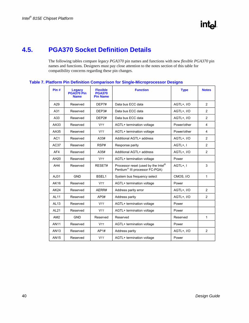
Intel® 815E Chipset Platform
R
40 Design Guide
4.5. PGA370 Socket Definition Details The following tables compare legacy PGA370 pin names and functions with new flexible PGA370 pin names and functions. Designers must pay close attention to the notes section of this table for compatibility concerns regarding these pin changes.
Table 7. Platform Pin Definition Comparison for Single-Microprocessor Designs
Pin # Legacy PGA370 Pin
Name
Flexible PGA370
Pin Name
Function Type Notes
A29 Reserved DEP7# Data bus ECC data AGTL+, I/O 2
A31 Reserved DEP3# Data bus ECC data AGTL+, I/O 2
A33 Reserved DEP2# Data bus ECC data AGTL+, I/O 2
AA33 Reserved VTT AGTL+ termination voltage Power/other 4
AA35 Reserved VTT AGTL+ termination voltage Power/other 4
AC1 Reserved A33# Additional AGTL+ address AGTL+, I/O 2
AC37 Reserved RSP# Response parity AGTL+, I 2
AF4 Reserved A35# Additional AGTL+ address AGTL+, I/O 2
AH20 Reserved VTT AGTL+ termination voltage Power
AH4 Reserved RESET# Processor reset (used by the Intel®
Pentium III processor FC-PGA) AGTL+, I 3
AJ31 GND BSEL1 System bus frequency select CMOS, I/O 1
AK16 Reserved VTT AGTL+ termination voltage Power
AK24 Reserved AERR# Address parity error AGTL+, I/O 2
AL11 Reserved AP0# Address parity AGTL+, I/O 2
AL13 Reserved VTT AGTL+ termination voltage Power
AL21 Reserved VTT AGTL+ termination voltage Power
AM2 GND Reserved Reserved Reserved 1
AN11 Reserved VTT AGTL+ termination voltage Power
AN13 Reserved AP1# Address parity AGTL+, I/O 2
AN15 Reserved VTT AGTL+ termination voltage Power

Intel® 815E Chipset Platform
R
Design Guide 41
Pin # Legacy
PGA370 Pin Name
Flexible PGA370
Pin Name
Function Type Notes
AN21 Reserved VTT AGTL+ termination voltage Power/other 4
AN23 Reserved RP# Request parity AGTL+, I/O
B36 Reserved BINIT# Bus initialization AGTL+, I/O 2
C29 Reserved DEP5# Data bus ECC data AGTL+, I/O 2
C31 Reserved DEP1# Data bus ECC data AGTL+, I/O 2
C33 Reserved DEP0# Data bus ECC data AGTL+, I/O 2
E23 Reserved VTT AGTL+ termination voltage Power/other 4
E29 Reserved DEP6# Data bus ECC data AGTL+, I/O 2
E31 Reserved DEP4# Data bus ECC data AGTL+, I/O 2
G35 Reserved VTT AGTL+ termination voltage Power/other
G37 Reserved See Note 5
S33 Reserved VTT AGTL+ termination voltage Power/other 4
S37 Reserved VTT AGTL+ termination voltage Power/other 4
U35 Reserved VTT AGTL+ termination voltage Power/other 4
U37 Reserved VTT AGTL+ termination voltage Power/other 4
V4 Reserved BERR# Bus error AGTL+, I/O 2
W3 Reserved A34# Additional AGTL+ address AGTL+, I/O 2
X4 RESET# RESET2# Processor reset (used by the Intel®
Celeron processor (PPGA)) AGTL+, I 3
X6 Reserved A32# Additional AGTL+ address AGTL+, I/O 2
Y33 GND CLKREF 1.25-V PLL reference Power 1 NOTES:
1. These signals are defined as ground (Vss) in legacy designs utilizing the PGA370 socket. For new flexible PGA370 designs, use the new signal definitions. These new signal definitions are backwards compatible with the Intel® Celeron processor (PPGA).
2. While these signals are not used with Intel® 815E chipset designs, they are available for chipsets that do support these functions. Only the Intel® Pentium® III processor (FC-PGA) offers these capabilities in the PGA370 platform.
3. The AGTL+ reset signal, RESET#, is delivered to pin X4 on legacy PGA370 designs. In flexible PGA370 designs, it is delivered to X4 and AH4 pins.
4. RESET2# is not required for platforms that do not support the Intel® Celeron™ processor. Pin X4 should then be connected to ground.
5. These pins must be connected to the 1.5-V VTT plane. 6. This pin must be connected to VTT for platforms using the Intel® Pentium® III processor based on
the cA2 stepping. Refer to the Intel® Pentium® III processor specification update for stepping details.
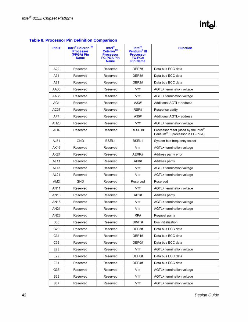
Intel® 815E Chipset Platform
R
42 Design Guide
Table 8. Processor Pin Definition Comparison
Pin # Intel® CeleronTM Processor (PPGA) Pin
Name
Intel® CeleronTM Processor
FC-PGA Pin Name
Intel®
Pentium® III Processor FC-PGA
Pin Name
Function
A29 Reserved Reserved DEP7# Data bus ECC data
A31 Reserved Reserved DEP3# Data bus ECC data
A33 Reserved Reserved DEP2# Data bus ECC data
AA33 Reserved Reserved VTT AGTL+ termination voltage
AA35 Reserved Reserved VTT AGTL+ termination voltage
AC1 Reserved Reserved A33# Additional AGTL+ address
AC37 Reserved Reserved RSP# Response parity
AF4 Reserved Reserved A35# Additional AGTL+ address
AH20 Reserved Reserved VTT AGTL+ termination voltage
AH4 Reserved Reserved RESET# Processor reset (used by the Intel®
Pentium® III processor in FC-PGA)
AJ31 GND BSEL1 BSEL1 System bus frequency select
AK16 Reserved Reserved VTT AGTL+ termination voltage
AK24 Reserved Reserved AERR# Address parity error
AL11 Reserved Reserved AP0# Address parity
AL13 Reserved Reserved VTT AGTL+ termination voltage
AL21 Reserved Reserved VTT AGTL+ termination voltage
AM2 GND Reserved Reserved Reserved
AN11 Reserved Reserved VTT AGTL+ termination voltage
AN13 Reserved Reserved AP1# Address parity
AN15 Reserved Reserved VTT AGTL+ termination voltage
AN21 Reserved Reserved VTT AGTL+ termination voltage
AN23 Reserved Reserved RP# Request parity
B36 Reserved Reserved BINIT# Bus initialization
C29 Reserved Reserved DEP5# Data bus ECC data
C31 Reserved Reserved DEP1# Data bus ECC data
C33 Reserved Reserved DEP0# Data bus ECC data
E23 Reserved Reserved VTT AGTL+ termination voltage
E29 Reserved Reserved DEP6# Data bus ECC data
E31 Reserved Reserved DEP4# Data bus ECC data
G35 Reserved Reserved VTT AGTL+ termination voltage
S33 Reserved Reserved VTT AGTL+ termination voltage
S37 Reserved Reserved VTT AGTL+ termination voltage
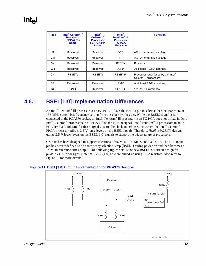
Intel® 815E Chipset Platform
R
Design Guide 43
Pin # Intel® CeleronTM Processor (PPGA) Pin
Name
Intel® CeleronTM Processor
FC-PGA Pin Name
Intel®
Pentium® III Processor FC-PGA
Pin Name
Function
U35 Reserved Reserved VTT AGTL+ termination voltage
U37 Reserved Reserved VTT AGTL+ termination voltage
V4 Reserved Reserved BERR# Bus error
W3 Reserved Reserved A34# Additional AGTL+ address
X4 RESET# RESET# RESET2# Processor reset (used by the Intel®
CeleronTM processors)
X6 Reserved Reserved A32# Additional AGTL+ address
Y33 GND Reserved CLKREF 1.25-V PLL reference
4.6. BSEL[1:0] Implementation Differences An Intel® Pentium® III processor in an FC-PGA utilizes the BSEL1 pin to select either the 100-MHz or 133-MHz system bus frequency setting from the clock synthesizer. While the BSEL0 signal is still connected to the PGA370 socket, an Intel® Pentium® III processor in an FC-PGA does not utilize it. Only Intel® Celeron™ processors in a PPGA utilize the BSEL0 signal. Intel® Pentium® III processors in an FC-PGA are 3.3-V tolerant for these signals, as are the clock and chipset. However, the Intel® Celeron™ PPGA processor utilizes 2.5-V logic levels on the BSEL signals. Therefore, flexible PGA370 designs utilize 2.5-V logic levels on the BSEL[1:0] signals to support the widest range of processors.
CK-815 has been designed to support selections of 66 MHz, 100 MHz, and 133 MHz. The REF input pin has been redefined to be a frequency selection strap (BSEL1) during power-on and then becomes a 14-MHz reference clock output. The following figure details the new BSEL[1:0] circuit design for flexible PGA370 designs. Note that BSEL[1:0] now are pulled up using 1-kΩ resistors. Also refer to Figure 12 for more details.
Figure 11. BSEL[1:0] Circuit Implementation for PGA370 Designs
Processor
BSEL0 BSEL1
Chipset
Clock Driver
1 kΩ1 kΩ
3.3 Vsus
10 kΩ
10 kΩ10 kΩ
sys_bus_BSEL_PGA370
14 MHz REFCLK
REF
SEL0
SEL1
3.3 Vsus
8.2 kΩ
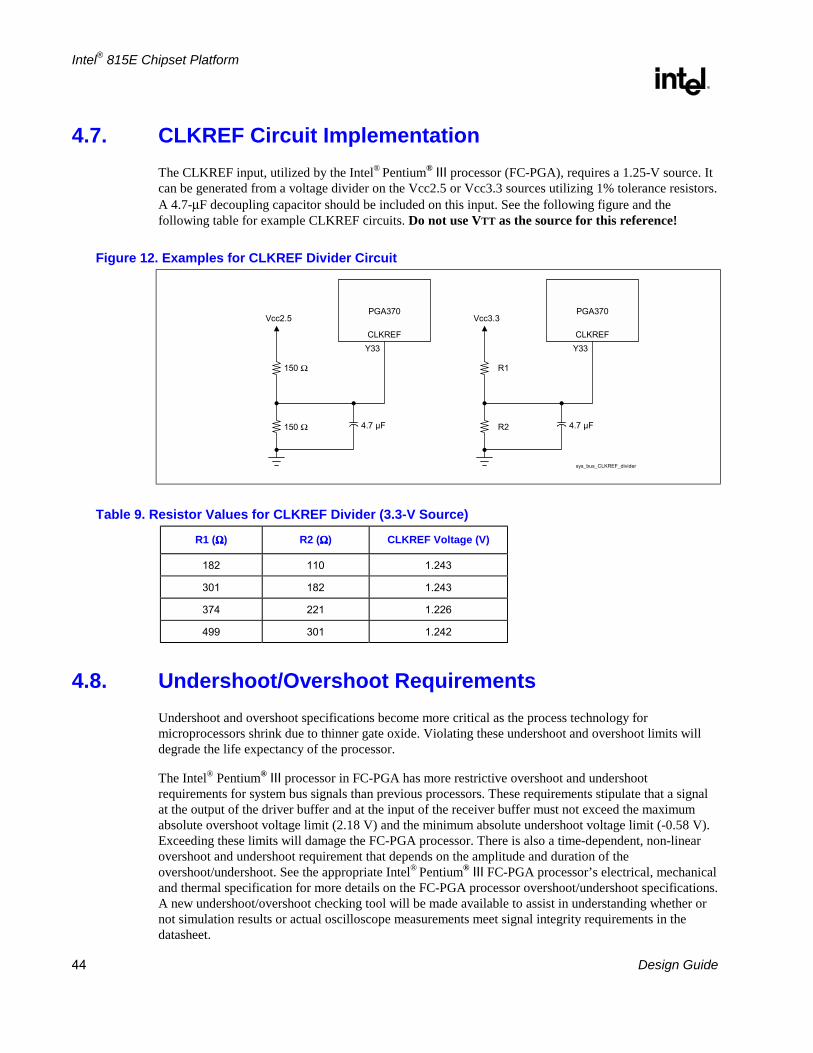
Intel® 815E Chipset Platform
R
44 Design Guide
4.7. CLKREF Circuit Implementation The CLKREF input, utilized by the Intel® Pentium® III processor (FC-PGA), requires a 1.25-V source. It can be generated from a voltage divider on the Vcc2.5 or Vcc3.3 sources utilizing 1% tolerance resistors. A 4.7-µF decoupling capacitor should be included on this input. See the following figure and the following table for example CLKREF circuits. Do not use VTT as the source for this reference!
Figure 12. Examples for CLKREF Divider Circuit
Vcc2.5
150 Ω
150 Ω
PGA370
CLKREFY33
4.7 µF
Vcc3.3
R1
R2
PGA370
CLKREFY33
4.7 µF
sys_bus_CLKREF_divider
Table 9. Resistor Values for CLKREF Divider (3.3-V Source)
R1 (ΩΩΩΩ) R2 (ΩΩΩΩ) CLKREF Voltage (V)
182 110 1.243
301 182 1.243
374 221 1.226
499 301 1.242
4.8. Undershoot/Overshoot Requirements Undershoot and overshoot specifications become more critical as the process technology for microprocessors shrink due to thinner gate oxide. Violating these undershoot and overshoot limits will degrade the life expectancy of the processor.
The Intel® Pentium® III processor in FC-PGA has more restrictive overshoot and undershoot requirements for system bus signals than previous processors. These requirements stipulate that a signal at the output of the driver buffer and at the input of the receiver buffer must not exceed the maximum absolute overshoot voltage limit (2.18 V) and the minimum absolute undershoot voltage limit (-0.58 V). Exceeding these limits will damage the FC-PGA processor. There is also a time-dependent, non-linear overshoot and undershoot requirement that depends on the amplitude and duration of the overshoot/undershoot. See the appropriate Intel® Pentium® III FC-PGA processor’s electrical, mechanical and thermal specification for more details on the FC-PGA processor overshoot/undershoot specifications. A new undershoot/overshoot checking tool will be made available to assist in understanding whether or not simulation results or actual oscilloscope measurements meet signal integrity requirements in the datasheet.
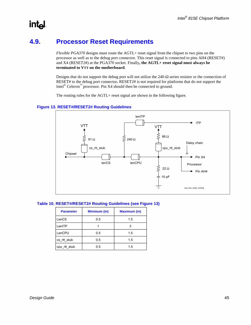
Intel® 815E Chipset Platform
R
Design Guide 45
4.9. Processor Reset Requirements Flexible PGA370 designs must route the AGTL+ reset signal from the chipset to two pins on the processor as well as to the debug port connector. This reset signal is connected to pins AH4 (RESET#) and X4 (RESET2#) at the PGA370 socket. Finally, the AGTL+ reset signal must always be terminated to VTT on the motherboard.
Designs that do not support the debug port will not utilize the 240-Ω series resistor or the connection of RESET# to the debug port connector. RESET2# is not required for platforms that do not support the Intel® Celeron™ processor. Pin X4 should then be connected to ground.
The routing rules for the AGTL+ reset signal are shown in the following figure.
Figure 13. RESET#/RESET2# Routing Guidelines
ITP
Pin X4
Processor
Pin AH4
lenITP
VTT
Daisy chain
10 pF
86 Ω
lenCPUlenCS
91 Ω
cs_rtt_stub
Chipset
VTT
240 Ω
22 Ω
cpu_rtt_stub
sys_bus_reset_routing
Table 10. RESET#/RESET2# Routing Guidelines (see Figure 13)
Parameter Minimum (in) Maximum (in)
LenCS 0.5 1.5
LenITP 1 3
LenCPU 0.5 1.5
cs_rtt_stub 0.5 1.5
cpu_rtt_stub 0.5 1.5

Intel® 815E Chipset Platform
R
46 Design Guide
4.10. Determining the Processor Installed Via Hardware Mechanisms The following table provides the logic decoding to determine which processor is installed in a PGA370 design.
Table 11. Determining the Installed Processor via Hardware Mechanisms
VID VCORE_DET CPUPRES# Notes
1001 0 0 Intel® Pentium® III processor (FC-PGA) installed.
1011 0 0 Intel® Celeron processor (FC-PGA) installed.
0001 1 0 Intel® Celeron processor (PPGA) installed.
1111 X 1 No processor installed.
4.11. Processor PLL Filter Recommendations Intel PGA370 processors have internal phase lock loop (PLL) clock generators that are analog and require quiet power supplies to minimize jitter.
4.11.1. Topology
The general desired topology is shown in Figure 15. Not shown are the parasitic routing and local decoupling capacitors. Excluded from the external circuitry are parasitics associated with each component.
4.11.2. Filter Specification
The function of the filter is to protect the PLL from external noise through low-pass attenuation. The low-pass specification, with input at VCCCORE and output measured across the capacitor, is as follows:
• < 0.2-dB gain in pass band
• < 0.5-dB attenuation in pass band (see DC drop in next set of requirements)
• > 34-dB attenuation from 1 MHz to 66 MHz
• > 28-dB attenuation from 66 MHz to core frequency
The filter specification is graphically shown in the following figure.

Intel® 815E Chipset Platform
R
Design Guide 47
Figure 14. Filter Specification
0dB
-28dB
-34dB
0.2dB
-0.5 dB
1 MHz 66 MHz fcorefpeak1HzDC
passband high frequencyband
filter_spec
ForbiddenZone
ForbiddenZone
NOTES:
1. Diagram not to scale. 2. No specification for frequencies beyond fcore. 3. fpeak should be less than 0.05 MHz.
Other requirements:
• Use shielded-type inductor to minimize magnetic pickup.
• Filter should support DC current > 30 mA.
• DC voltage drop from VCC to PLL1 should be < 60 mV, which in practice implies series R < 2 Ω. This also means pass-band (from DC to 1 Hz) attenuation < 0.5 dB for VCC = 1.1 V, and < 0.35 dB for VCC = 1.5 V.

Intel® 815E Chipset Platform
R
48 Design Guide
4.11.3. Recommendation for Intel® Platforms
The following tables contains examples of components that meet Intel’s recommendations, when configured in the topology of Figure 15.
Table 12. Component Recommendations – Inductor
Part Number Value Tol. SRF Rated I DCR (Typical)
TDK MLF2012A4R7KT 4.7 µH 10% 35 MHz 30 mA 0.56 Ω (1 Ω max.)
Murata LQG21N4R7K00T1 4.7 µH 10% 47 MHz 30 mA 0.7 Ω (± 50%)
Murata LQG21C4R7N00 4.7 µH 30% 35 MHz 30 mA 0.3 Ω max.
Table 13. Component Recommendations – Capacitor
Part Number Value Tolerance ESL ESR
Kemet T495D336M016AS 33 µF 20% 2.5 nH 0.225 Ω
AVX TPSD336M020S0200 33 µF 20% 2.5 nH 0.2 Ω
Table 14. Component Recommendations – Resistor
Value Tolerance Power Note
1 Ω 10% 1/16 W Resistor may be implemented with trace resistance, in which case a discrete R is not needed.
To satisfy damping requirements, total series resistance in the filter (from VCCCORE to the top plate of the capacitor) must be at least 0.35 Ω. This resistor can be in the form of a discrete component or routing or both. For example, if the picked inductor has minimum DCR of 0.25 Ω, then a routing resistance of at least 0.10 Ω is required. Be careful not to exceed the maximum resistance rule (2 Ω). For example, if using discrete R1 (1 Ω ± 1%), the maximum DCR of the L (trace plus inductor) should be less than 2.0 - 1.1 = 0.9 Ω, which precludes the use of some inductors and sets a max. trace length.
Other routing requirements:
• The capacitor (C) should be close to the PLL1 and PLL2 pins, < 0.1 Ω per route1.
• The PLL2 route should be parallel and next to the PLL1 route (i.e., minimize loop area).
• The inductor (L) should be close to C. Any routing resistance should be inserted between VCCCORE and L.
• Any discrete resistor (R) should be inserted between VCCCORE and L.
1 These routes do not count towards the minimum damping R requirement.
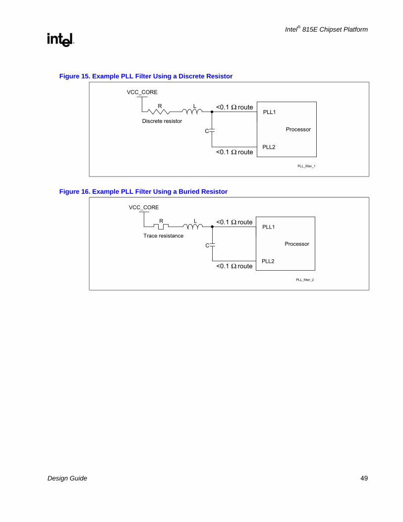
Intel® 815E Chipset Platform
R
Design Guide 49
Figure 15. Example PLL Filter Using a Discrete Resistor
Processor
PLL1
PLL2
C
LR
VCC_CORE
PLL_filter_1
Discrete resistor
<0.1 Ω route
<0.1 Ω route
Figure 16. Example PLL Filter Using a Buried Resistor
Processor
PLL1
PLL2
C
LR
VCC_CORE
PLL_filter_2
Trace resistance
<0.1 Ω route
<0.1 Ω route
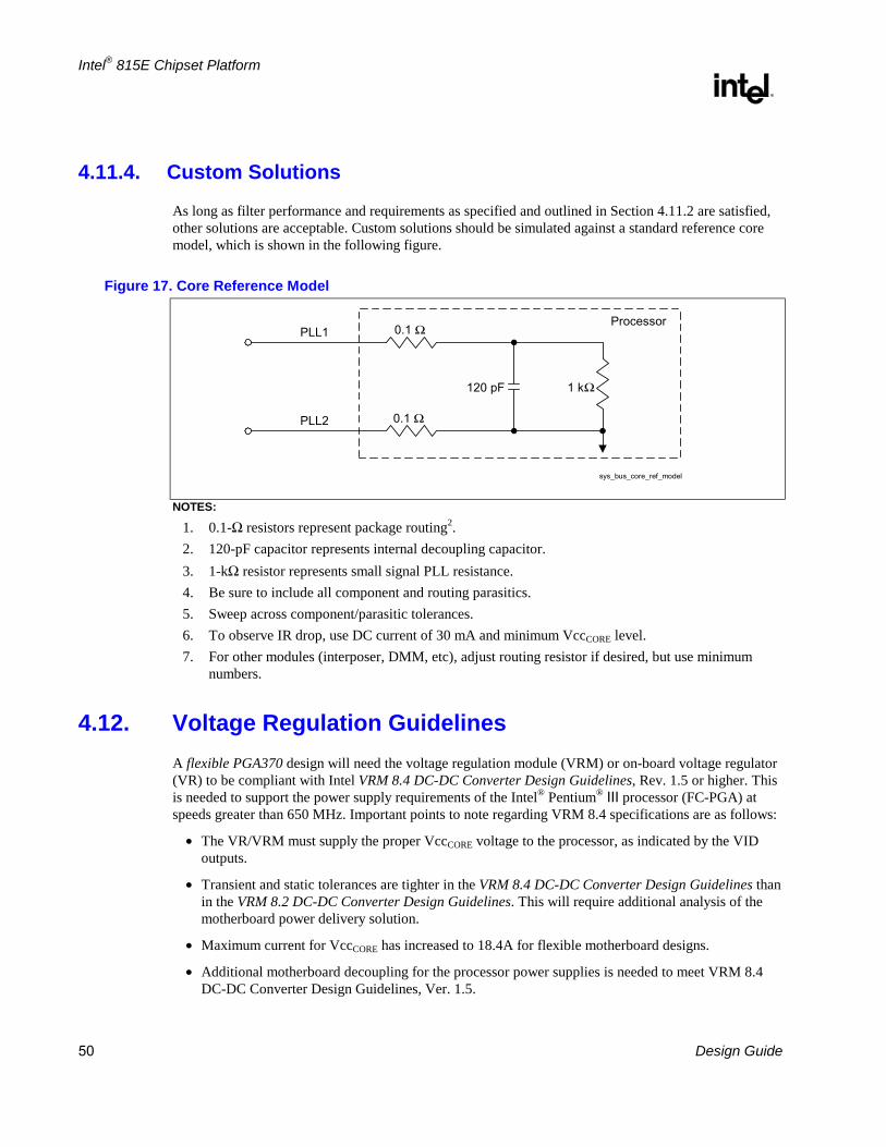
Intel® 815E Chipset Platform
R
50 Design Guide
4.11.4. Custom Solutions
As long as filter performance and requirements as specified and outlined in Section 4.11.2 are satisfied, other solutions are acceptable. Custom solutions should be simulated against a standard reference core model, which is shown in the following figure.
Figure 17. Core Reference Model
PLL1
PLL2
sys_bus_core_ref_model
0.1 Ω
0.1 Ω
120 pF 1 kΩ
Processor
NOTES:
1. 0.1-Ω resistors represent package routing2. 2. 120-pF capacitor represents internal decoupling capacitor. 3. 1-kΩ resistor represents small signal PLL resistance. 4. Be sure to include all component and routing parasitics. 5. Sweep across component/parasitic tolerances. 6. To observe IR drop, use DC current of 30 mA and minimum VccCORE level. 7. For other modules (interposer, DMM, etc), adjust routing resistor if desired, but use minimum
numbers.
4.12. Voltage Regulation Guidelines A flexible PGA370 design will need the voltage regulation module (VRM) or on-board voltage regulator (VR) to be compliant with Intel VRM 8.4 DC-DC Converter Design Guidelines, Rev. 1.5 or higher. This is needed to support the power supply requirements of the Intel® Pentium® III processor (FC-PGA) at speeds greater than 650 MHz. Important points to note regarding VRM 8.4 specifications are as follows:
• The VR/VRM must supply the proper VccCORE voltage to the processor, as indicated by the VID outputs.
• Transient and static tolerances are tighter in the VRM 8.4 DC-DC Converter Design Guidelines than in the VRM 8.2 DC-DC Converter Design Guidelines. This will require additional analysis of the motherboard power delivery solution.
• Maximum current for VccCORE has increased to 18.4A for flexible motherboard designs.
• Additional motherboard decoupling for the processor power supplies is needed to meet VRM 8.4 DC-DC Converter Design Guidelines, Ver. 1.5.
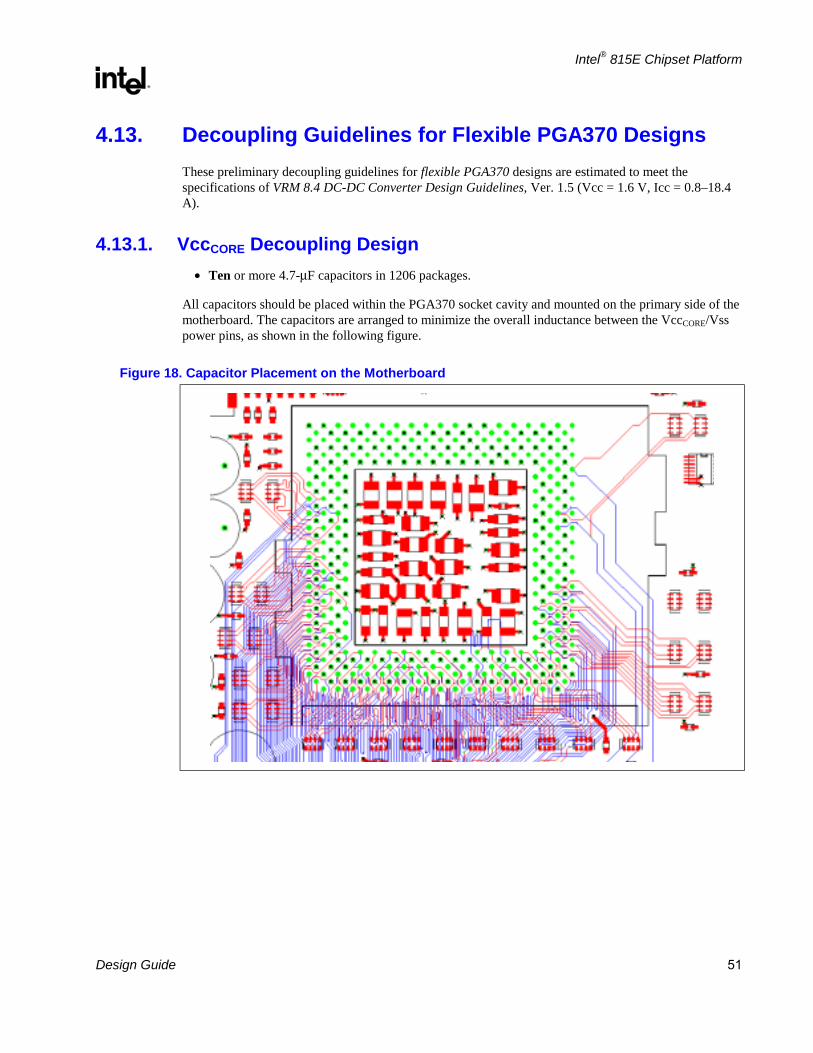
Intel® 815E Chipset Platform
R
Design Guide 51
4.13. Decoupling Guidelines for Flexible PGA370 Designs These preliminary decoupling guidelines for flexible PGA370 designs are estimated to meet the specifications of VRM 8.4 DC-DC Converter Design Guidelines, Ver. 1.5 (Vcc = 1.6 V, Icc = 0.8–18.4 A).
4.13.1. VccCORE Decoupling Design • Ten or more 4.7-µF capacitors in 1206 packages.
All capacitors should be placed within the PGA370 socket cavity and mounted on the primary side of the motherboard. The capacitors are arranged to minimize the overall inductance between the VccCORE/Vss power pins, as shown in the following figure.
Figure 18. Capacitor Placement on the Motherboard
Intel® 815E Chipset Platform
R
52 Design Guide
4.13.2. VTT Decoupling Design
For Itt = 3.0 A (max.)
• Nineteen 0.1-µF capacitors in 0603 packages placed within 200 mils of AGTL+ termination R-packs, with one capacitor for every two R-packs. These capacitors are shown on the exterior of the previous figure.
4.13.3. VREF Decoupling Design • Four 0.1-µF capacitors in 0603 package placed near VREF pins (within 500 mils).
4.14. Thermal/EMI Considerations Flexible motherboard guideline for the Intel® Pentium® III processor (FC-PGA) calls for 30.4 W.
• Increased power density for the Intel® Pentium® III processor in FC-PGA (FMB = 41.9 W/cm2)
• Intel® Pentium® III processors in FC-PGA are specified using Tj, while PPGA processors are specified using Tcase.
• Heatsink for FC-PGA package is not compatible with PPGA processors
• New heatsink clips for FC-PGA processor heatsinks
• Option to add motherboard features to ground the processor heatsink to reduce electromagnetic interference (EMI)
4.14.1. Implementation of Optional Grounded Heatsink for EMI Reduction
The following figure illustrates the concept of providing the processor heatsink with an AC ground return path. Experiments at Intel have demonstrated improved EMI emissions with prototypes of this solution. Further details will be provided in the next revision of this design guide.

Intel® 815E Chipset Platform
R
Design Guide 53
Figure 19. Location of Grounding Pads
Loc_GND_Pads
2.215
0.415
PGA370
1.350
See Detail A
A10.450
Detail AScale 8.000
4X 0.255
4X 0.175
4X 0.400
4X 0.450
ComponentKeep-Out
Ground Pad
4.14.2. Heat Sink Volumetric Keep Out Regions
Figure 20 shows the system component keep-out volume above the socket connector required for the reference design thermal solution for high frequency FC-PGA processors. This keep-out envelope provides adequate room for the heat sink, fan and attach hardware under static conditions as well as room for installation of these components on the socket.
Figure 21 shows component keep-outs on the motherboard required to prevent interference with the reference design thermal solution. Note portions of the heat sink and attach hardware hang over the motherboard.
Adhering to these keep-out areas will ensure compatibility with Intel boxed processor products and Intel enabled third party vendor thermal solutions for FC-PGA processors. While the keep-out requirements should provide adequate space for the reference design thermal solution, systems integrators should check their vendor to ensure their specific thermal solutions fit within their specific system designs. Please ensure that the thermal solutions under analysis comprehend the specific thermal design requirements for higher frequency Pentium® III processors.
While thermal solutions for lower frequency FCPGA processors may not require the full keep-out area, larger thermal solutions will be required for higher frequency processors and failure to adhere to the guidelines will result in mechanical interference.
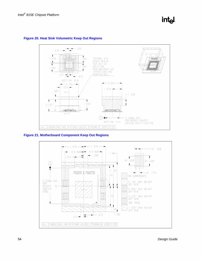
Intel® 815E Chipset Platform
R
54 Design Guide
Figure 20. Heat Sink Volumetric Keep Out Regions
Figure 21. Motherboard Component Keep Out Regions

Intel® 815E Chipset Platform
R
Design Guide 55
4.15. Debug Port Changes Due to the lower voltage technology employed with the FC-PGA processor, changes are required to support the debug port. Previously, test access port (TAP) signals used 2.5-V logic, as is the case with the Intel® Celeron™ processor in the PPGA package. FC-PGA processors utilize 1.5-V logic levels on the TAP. As a result, a new debug port connector is to be used in flexible PGA370 designs. The new 1.5-V connector is the mirror image of the older 2.5-V connector. Either connector will fit into the same printed circuit board layout. Only the pin numbers would change, as is evident in the following drawing. Also required, along with the new connector, is an In-Target Probe (ITP) that is capable of communicating with the TAP at 1.5-V logic levels.
Figure 22. TAP Connector Comparison
2 4 6 8 10 12 14 16 18 20 22 24 26 28 30
1 3 5 7 9 11 13 15 17 19 21 23 25 27 29
1 3 5 7 9 11 13 15 17 19 21 23 25 27 29
2 4 6 8 10 12 14 16 18 20 22 24 26 28 30
RESET#
RESET#
2.5 V connector, AMP 104068-3 vertical plug, top view
1.5 V connector, AMP 104078-4 vertical receptacle, top view
sys_bus_TAP_conn
Caution: FC-PGA processors require an in-target probe (ITP) compatible with 1.5-V signal levels on the TAP. Previous ITPs were designed to work with higher voltages and may damage the processor if connected to an FC-PGA processor.
See the processor datasheet for more information regarding the debug port.

Intel® 815E Chipset Platform
R
56 Design Guide
This page intentionally left blank.
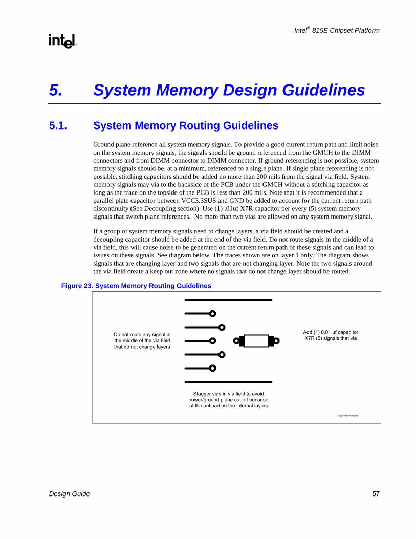
Intel® 815E Chipset Platform
R
Design Guide 57
5. System Memory Design Guidelines
5.1. System Memory Routing Guidelines Ground plane reference all system memory signals. To provide a good current return path and limit noise on the system memory signals, the signals should be ground referenced from the GMCH to the DIMM connectors and from DIMM connector to DIMM connector. If ground referencing is not possible, system memory signals should be, at a minimum, referenced to a single plane. If single plane referencing is not possible, stitching capacitors should be added no more than 200 mils from the signal via field. System memory signals may via to the backside of the PCB under the GMCH without a stitching capacitor as long as the trace on the topside of the PCB is less than 200 mils. Note that it is recommended that a parallel plate capacitor between VCC3.3SUS and GND be added to account for the current return path discontinuity (See Decoupling section). Use (1) .01uf X7R capacitor per every (5) system memory signals that switch plane references. No more than two vias are allowed on any system memory signal.
If a group of system memory signals need to change layers, a via field should be created and a decoupling capacitor should be added at the end of the via field. Do not route signals in the middle of a via field, this will cause noise to be generated on the current return path of these signals and can lead to issues on these signals. See diagram below. The traces shown are on layer 1 only. The diagram shows signals that are changing layer and two signals that are not changing layer. Note the two signals around the via field create a keep out zone where no signals that do not change layer should be routed.
Figure 23. System Memory Routing Guidelines
Do not route any signal inthe middle of the via fieldthat do not change layers
Add (1) 0.01 uf capacitorX7R (5) signals that via
Stagger vias in via field to avoidpower/ground plane cut off becauseof the antipad on the internal layers
sys-mem-route
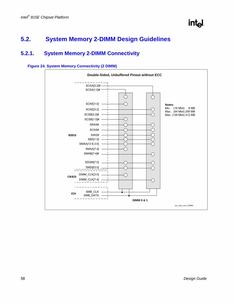
Intel® 815E Chipset Platform
R
58 Design Guide
5.2. System Memory 2-DIMM Design Guidelines
5.2.1. System Memory 2-DIMM Connectivity
Figure 24. System Memory Connectivity (2 DIMM)
SCSA[3:2]#SCSA[1:0]#
SCKE[1:0]
SCKE[3:2]
SRAS#
SCAS#
SWE#SBS[1:0]
SMAA[12:8,3:0]
SMAA[7:4]SMAB[7:4]#
SDQM[7:0]
SMD[63:0]
DIMM_CLK[3:0]
DIMM_CLK[7:4]
SMB_CLKSMB_DATA
Notes:Min. (16 Mbit) 8 MBMax. (64 Mbit) 256 MBMax. (128 Mbit) 512 MB
sys_mem_conn_2DIMM
SCSB[3:2]#
SCSB[1:0]#
DIMM 0 & 1
ICH
CK815
82815
Double-Sided, Unbuffered Pinout without ECC

Intel® 815E Chipset Platform
R
Design Guide 59
5.2.2. System Memory 2-DIMM Layout Guidelines
Due to the lower voltage technology employed with the FC-PGA processor, changes are required to support the debug port. Previously, test access port (TAP) signals used 2.5-V logic, as is the case with the Intel® Celeron™ processor in the PPGA package. FC-PGA processors utilize 1.5-V logic levels on the
Figure 25. System Memory 2-DIMM Routing Topologies
Topology 1
82815
Topology 2
Topology 3
Topology 4
Topology 5
sys_mem_2DIMM_routing_topo
A
C
D
F
F
10 Ω
10 ΩE
E
B
DIMM 0 DIMM 1
Table 15. System Memory 2-DIMM Solution Space
Trace Lengths (inches) Trace (mils)
A B C D E F
Signal Top.
Width Spacing Min. Max. Min. Max. Min. Max. Min. Max. Min. Max. Min. Max.
SCS[3:2]# 3 5 10 1 4.5
SCS[1:0]# 2 5 10 1 4.5
SMAA[7:4] 4 10 10 0.4 0.5 2 4
SMAB[7:4]# 5 10 10 0.4 0.5 2 4
SCKE[3:2] 3 10 10 3 4
SCKE[1:0] 2 10 10 3 4
SMD[63:0] 1 5 10 1.75 4 0.4 0.5
SDQM[7:0] 1 10 10 1.5 3.5 0.4 0.5
SCAS#, SRAS#, SWE# 1 5 10 1 4.0 0.4 0.5
SBS[1:0], SMAA[12:8,3:0]
1 5 10 1 4.0 0.4 0.5
In addition to meeting the spacing requirements outlined in Table 15, system memory signal trace edges must be at least 30 mils from any other non-system memory signal trace edge.
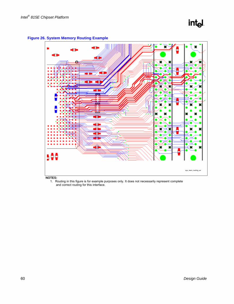
Intel® 815E Chipset Platform
R
60 Design Guide
Figure 26. System Memory Routing Example
sys_mem_routing_ex NOTES:
1. Routing in this figure is for example purposes only. It does not necessarily represent complete and correct routing for this interface.
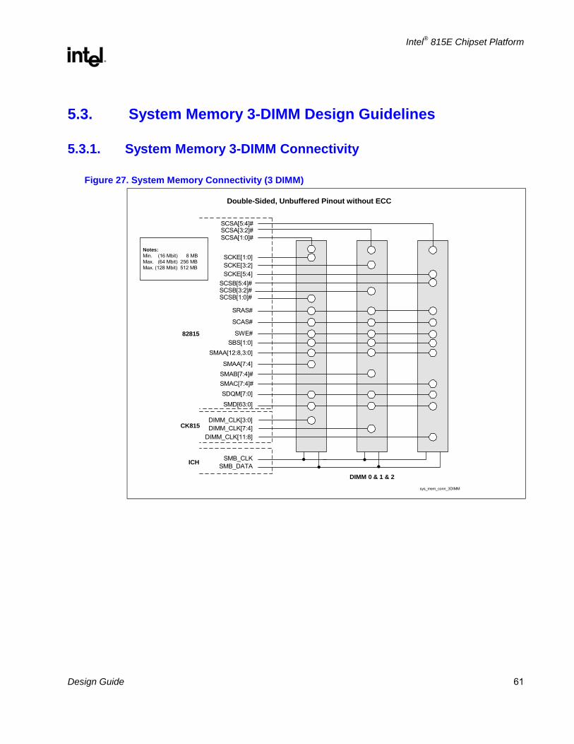
Intel® 815E Chipset Platform
R
Design Guide 61
5.3. System Memory 3-DIMM Design Guidelines
5.3.1. System Memory 3-DIMM Connectivity
Figure 27. System Memory Connectivity (3 DIMM)
SCSA[3:2]#SCSA[1:0]#
SCKE[1:0]SCKE[3:2]
SRAS#
SCAS#
SWE#SBS[1:0]
SMAA[12:8,3:0]
SMAA[7:4]SMAB[7:4]#
SDQM[7:0]
SMD[63:0]
DIMM_CLK[3:0]DIMM_CLK[7:4]
SMB_CLKSMB_DATA
sys_mem_conn_3DIMM
SCSB[3:2]#SCSB[1:0]#
DIMM 0 & 1 & 2
ICH
CK815
82815
Double-Sided, Unbuffered Pinout without ECC
SCSA[5:4]#
SCKE[5:4]SCSB[5:4]#
SMAC[7:4]#
DIMM_CLK[11:8]
Notes:Min. (16 Mbit) 8 MBMax. (64 Mbit) 256 MBMax. (128 Mbit) 512 MB

Intel® 815E Chipset Platform
R
62 Design Guide
5.3.2. System Memory 3-DIMM Layout Guidelines
Figure 28. System Memory 3-DIMM Routing Topologies
Topology 1
82815
Topology 2
Topology 3
Topology 6
Topology 7
sys_mem_3DIMM_routing_topo
A
C
D
C
D
10 Ω
10 Ω
G
G
DIMM 0 DIMM 1
B
DIMM 2
B
Topology 4 E
Topology 5 F
Topology 8 E10 Ω
G
B B

Intel® 815E Chipset Platform
R
Design Guide 63
Table 16. System Memory 3-DIMM Solution Space
Trace Lengths (inches) Trace (mils)
A B C D E F G
Signal
Top. Width Spacing Min. Max. Min. Max. Min. Max. Min. Max. Min. Max. Min. Max. Min. Max.
SCS[5:4]# 4 5 10 1 4.5
SCS[3:2]# 3 5 10 1 4.5
SCS[1:0]# 2 5 10 1 4.5
SMAA[7:4] 6 10 10 2 4 0.4 0.5
SMAB[7:4]# 7 10 10 2 4 0.4 0.5
SMAC[7:4 8 10 10 2 4 0.4 0.5
SCKE[5:4] 4 10 10 3 4
SCKE[3:2] 3 10 10 3 4
SCKE[1:0] 2 10 10 3 4
SMD[63:0] 1 5 10 1.75 4 0.4 0.5
SDQM[7:0] 1 10 10 1.5 3.5 0.4 0.5
SCAS#, SRAS#, SWE#
5 5 10 0.4 0.5 1 4
SBS[1:0], SMAA[12:8,3:0]
5 5 10 0.4 0.5 1 4
In addition to meeting the spacing requirements outlined in Table 16, system memory signal trace edges must be at least 30 mils from any other non-system memory signal trace edge.
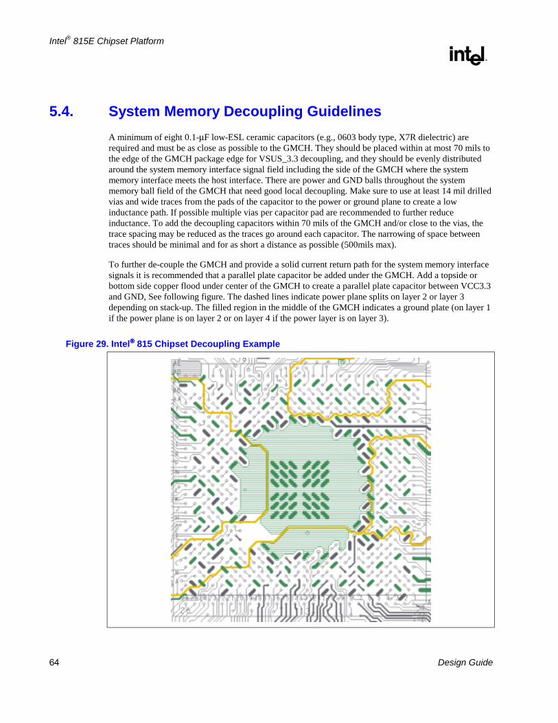
Intel® 815E Chipset Platform
R
64 Design Guide
5.4. System Memory Decoupling Guidelines A minimum of eight 0.1-µF low-ESL ceramic capacitors (e.g., 0603 body type, X7R dielectric) are required and must be as close as possible to the GMCH. They should be placed within at most 70 mils to the edge of the GMCH package edge for VSUS_3.3 decoupling, and they should be evenly distributed around the system memory interface signal field including the side of the GMCH where the system memory interface meets the host interface. There are power and GND balls throughout the system memory ball field of the GMCH that need good local decoupling. Make sure to use at least 14 mil drilled vias and wide traces from the pads of the capacitor to the power or ground plane to create a low inductance path. If possible multiple vias per capacitor pad are recommended to further reduce inductance. To add the decoupling capacitors within 70 mils of the GMCH and/or close to the vias, the trace spacing may be reduced as the traces go around each capacitor. The narrowing of space between traces should be minimal and for as short a distance as possible (500mils max).
To further de-couple the GMCH and provide a solid current return path for the system memory interface signals it is recommended that a parallel plate capacitor be added under the GMCH. Add a topside or bottom side copper flood under center of the GMCH to create a parallel plate capacitor between VCC3.3 and GND, See following figure. The dashed lines indicate power plane splits on layer 2 or layer 3 depending on stack-up. The filled region in the middle of the GMCH indicates a ground plate (on layer 1 if the power plane is on layer 2 or on layer 4 if the power layer is on layer 3).
Figure 29. Intel 815 Chipset Decoupling Example
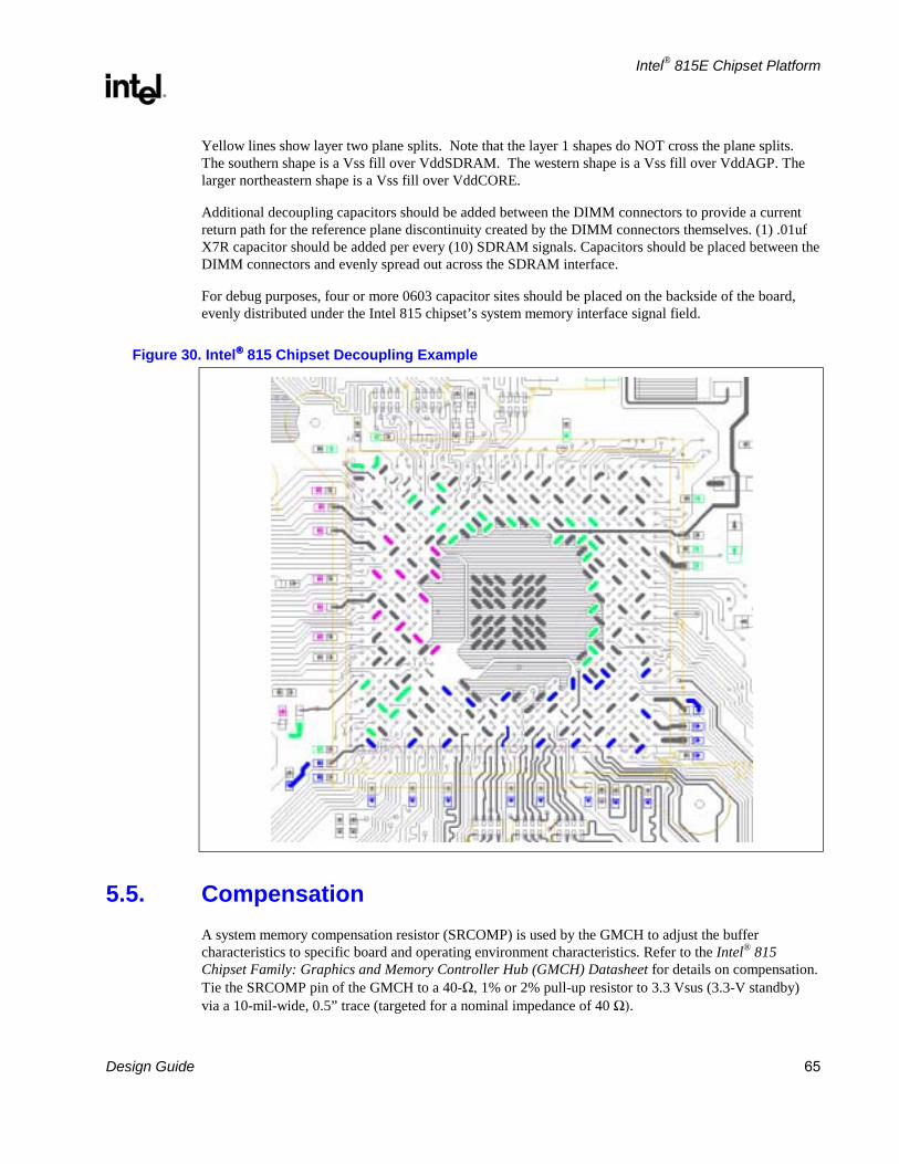
Intel® 815E Chipset Platform
R
Design Guide 65
Yellow lines show layer two plane splits. Note that the layer 1 shapes do NOT cross the plane splits. The southern shape is a Vss fill over VddSDRAM. The western shape is a Vss fill over VddAGP. The larger northeastern shape is a Vss fill over VddCORE.
Additional decoupling capacitors should be added between the DIMM connectors to provide a current return path for the reference plane discontinuity created by the DIMM connectors themselves. (1) .01uf X7R capacitor should be added per every (10) SDRAM signals. Capacitors should be placed between the DIMM connectors and evenly spread out across the SDRAM interface.
For debug purposes, four or more 0603 capacitor sites should be placed on the backside of the board, evenly distributed under the Intel 815 chipset’s system memory interface signal field.
Figure 30. Intel 815 Chipset Decoupling Example
5.5. Compensation A system memory compensation resistor (SRCOMP) is used by the GMCH to adjust the buffer characteristics to specific board and operating environment characteristics. Refer to the Intel® 815 Chipset Family: Graphics and Memory Controller Hub (GMCH) Datasheet for details on compensation. Tie the SRCOMP pin of the GMCH to a 40-Ω, 1% or 2% pull-up resistor to 3.3 Vsus (3.3-V standby) via a 10-mil-wide, 0.5” trace (targeted for a nominal impedance of 40 Ω).
Intel® 815E Chipset Platform
R
66 Design Guide
This page intentionally left blank.

Intel® 815E Chipset Platform
R
Design Guide 67
6. AGP/Display Cache Design Guidelines For the detailed AGP interface functionality (e.g., protocols, rules, signaling mechanisms), refer to the latest AGP Interface Specification, Revision 2.0, which can be obtained from http://www.agpforum.org. This design guide focuses only on specific Intel® 815E chipset platform recommendations.
6.1. AGP Interface A single AGP connector is supported by the GMCH AGP interface. LOCK# and SERR#/PERR# are not supported. See the display cache discussion for a description of display cache/AGP muxing as well as a description of the AGP In-Line Memory Module (AIMM).
The AGP buffers operate in one of two selectable modes, to support the AGP universal connector: 1. 3.3-V drive, not 5-V safe. This mode is compliant with the AGP 1.0 66-MHz specification 2. 1.5-V drive, not 3.3-V safe. This mode is compliant with the AGP 2.0 specification
The AGP 4X must operate at 1.5 V. The AGP 2X can operate at 3.3 V or 1.5 V. The AGP interface supports up to 4X AGP signaling, though 4X fast writes are not supported. AGP semantic cycles to DRAM are not snooped on the host bus.
The GMCH supports PIPE# or SBA[7:0] AGP address mechanisms, but not both simultaneously. Either the PIPE# or the SBA[7:0] mechanism must be selected during system initialization. The GMCH contains a 32-deep AGP request queue. High-priority accesses are supported. All AGP semantic accesses hitting the graphics aperture pass through an address translation mechanism with a fully-associative, 20-entry TLB.
Accesses between AGP and the hub interface are limited to hub interface-originated memory writes to AGP. Cacheable accesses from the IOQ queue flow through one path, while aperture accesses follow another path. Cacheable AGP (SBA, PIPE# and FRAME#) reads to DRAM all snoop the cacheable global write buffer (GWB) for system data coherency. Aperture AGP (SBA, PIPE#) reads to DRAM snoop the aperture queue (GCMCRWQ). Aperture AGP (FRAME#) reads and writes to DRAM proceed through a FIFO and there is no RAW capability, so no snoop is required.
The AGP interface is clocked from the 66-MHz clock (3V66). The AGP-to-host/memory interface is synchronous with a clock ratio of 1:1 (66 MHz : 66 MHz), 2:3 (66 MHz : 100 MHz) and 1:2 (66 MHz : 133 MHz).

Intel® 815E Chipset Platform
R
68 Design Guide
6.1.1. AGP In-Line Memory Module (AIMM)
The GMCH multiplexes the AGP signal interface with the integrated graphics’ display cache interface. As a result, for a flexible motherboard that supports both integrated graphics and add-in AGP video cards, display cache (for integrated graphics) must be populated on a card in the universal AGP slot. The card is called an AGP In-Line Memory Module (AIMM) card. Intel provides a specification for this card in a separate document (AGP Inline Memory Module Specification).
AGP guidelines are presented in this section for motherboards that support the population of an AIMM card in their AGP slot, as well as for those that do not. Where there are distinct guidelines dependent on whether or not a motherboard will support an AIMM card, the section detailing routing guidelines is broken into subsections, as follows:
• The Flexible Motherboard Guidelines subsection is to be complied with if the motherboard supports an AIMM card populated in the AGP slot.
• The AGP-Only Motherboard Guidelines subsection is to be complied with if the motherboard will NOT support an AIMM card populated in the AGP slot.
6.1.2. AGP Universal Retention Mechanism (RM)
Environmental testing and field reports indicate that AGP cards and AGP In Line Memory Module (AIMM) cards may come unseated during system shipping and handling without proper retention. To avoid disengaged AGP cards and AIMM modules, Intel recommends that AGP based platforms use the AGP retention mechanism (RM).
The AGP RM is a mounting bracket that is used to properly locate the card with respect to the chassis and to assist with card retention. The AGP RM is available in two different handle orientations: left-handed (see Figure 31) and right-handed. Most system boards accommodate the left-handed AGP RM. The manufacturing capacity of the left-handed RM currently exceeds the right-handed capacity, and as a result Intel recommends that customers design their systems to insure they can use the left-handed version of the AGP RM (see Figure 32). The right-handed AGP RM is identical to the left-handed AGP RM, except for the position of the actuation handle. This handle is located on the same end as the primary design, but extends from the opposite side (mirrored about the center axis running parallel to the length of the part). Figure 32 contains keep out information for the left hand AGP retention mechanism. Use this information to make sure that your motherboard design leaves adequate space to install the retention mechanism.
The AGP interconnect design requires that the AGP card must be retained to the extent that the card not back out more than 0.99 mm (0.039 in) within the AGP connector. To accomplish this it is recommended that new cards implement an additional notch feature in the mechanical keying tab to allow an anchor point on the AGP card for interfacing with an AGP RM. The retention mechanism’s round peg engages with the AGP or AIMM card’s retention tab and prevents the card from disengaging during dynamic loading. The additional notch feature in the mechanical keying tab is required for 1.5-volt AGP cards and is recommended for the new 3.3-volt AGP cards.
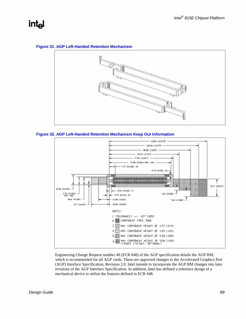
Intel® 815E Chipset Platform
R
Design Guide 69
Figure 31. AGP Left-Handed Retention Mechanism
Figure 32. AGP Left-Handed Retention Mechanism Keep Out Information
Engineering Change Request number 48 (ECR #48) of the AGP specification details the AGP RM, which is recommended for all AGP cards. These are approved changes to the Accelerated Graphics Port (AGP) Interface Specification, Revision 2.0. Intel intends to incorporate the AGP RM changes into later revisions of the AGP Interface Specification. In addition, Intel has defined a reference design of a mechanical device to utilize the features defined in ECR #48.
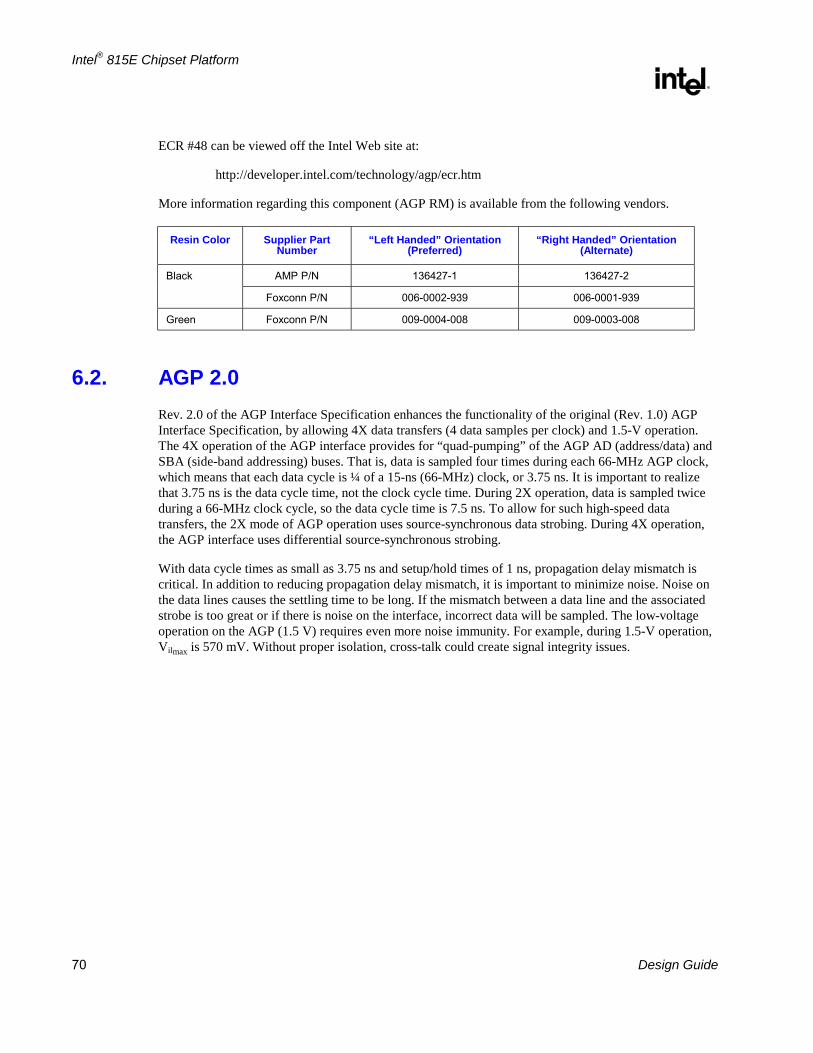
Intel® 815E Chipset Platform
R
70 Design Guide
ECR #48 can be viewed off the Intel Web site at:
http://developer.intel.com/technology/agp/ecr.htm
More information regarding this component (AGP RM) is available from the following vendors.
Resin Color Supplier Part Number
“Left Handed” Orientation (Preferred)
“Right Handed” Orientation (Alternate)
AMP P/N 136427-1 136427-2 Black
Foxconn P/N 006-0002-939 006-0001-939
Green Foxconn P/N 009-0004-008 009-0003-008
6.2. AGP 2.0 Rev. 2.0 of the AGP Interface Specification enhances the functionality of the original (Rev. 1.0) AGP Interface Specification, by allowing 4X data transfers (4 data samples per clock) and 1.5-V operation. The 4X operation of the AGP interface provides for “quad-pumping” of the AGP AD (address/data) and SBA (side-band addressing) buses. That is, data is sampled four times during each 66-MHz AGP clock, which means that each data cycle is ¼ of a 15-ns (66-MHz) clock, or 3.75 ns. It is important to realize that 3.75 ns is the data cycle time, not the clock cycle time. During 2X operation, data is sampled twice during a 66-MHz clock cycle, so the data cycle time is 7.5 ns. To allow for such high-speed data transfers, the 2X mode of AGP operation uses source-synchronous data strobing. During 4X operation, the AGP interface uses differential source-synchronous strobing.
With data cycle times as small as 3.75 ns and setup/hold times of 1 ns, propagation delay mismatch is critical. In addition to reducing propagation delay mismatch, it is important to minimize noise. Noise on the data lines causes the settling time to be long. If the mismatch between a data line and the associated strobe is too great or if there is noise on the interface, incorrect data will be sampled. The low-voltage operation on the AGP (1.5 V) requires even more noise immunity. For example, during 1.5-V operation, Vilmax is 570 mV. Without proper isolation, cross-talk could create signal integrity issues.
Intel® 815E Chipset Platform
R
Design Guide 71
6.2.1. AGP Interface Signal Groups
The signals on the AGP interface are broken into three groups: 1X timing domain signals, 2X/4X timing domain signals, and miscellaneous signals. Each group has different routing requirements. In addition, within the 2X/4X timing domain signals, there are three sets of signals. All signals in the 2X/4X timing domain must meet minimum and maximum trace length requirements as well as trace width and spacing requirements. However, trace length matching requirements only must be satisfied within each set of 2X/4X timing domain signals. The signal groups are listed in the following table.
Table 17. AGP 2.0 Signal Groups
Groups Signal
1X Timing Domain CLK (3.3 V), RBF#, WBF#, ST[2:0], PIPE#, REQ#, GNT#, PAR, FRAME#, IRDY#, TRDY#, STOP#, DEVSEL#
2X/4X Timing Domain Set #1: AD[15:0], C/BE[1:0]#, AD_STB0, AD_STB0#1
Set #2: AD[31:16], C/BE[3:2]#, AD_STB1, AD_STB1#1
Set #3: SBA[7:0], SB_STB, SB_STB#1
Miscellaneous, async. USB+, USB-, OVRCNT#, PME#, TYPDET#, PERR#, SERR#, INTA#, INTB#
NOTES: 1. These signals are used in 4X AGP mode ONLY.
Table 18. AGP 2.0 Data/Strobe Associations
Data Associated Strobe in 1X Associated Strobe in 2X
Associated Strobes in 4X
AD[15:0] and C/BE[1:0]#
Strobes are not used in 1X mode. All data is sampled on rising clock edges.
AD_STB0 AD_STB0, AD_STB0#
AD[31:16] and C/BE[3:2]#
Strobes are not used in 1X mode. All data is sampled on rising clock edges.
AD_STB1 AD_STB1, AD_STB1#
SBA[7:0] Strobes are not used in 1X mode. All data is sampled on rising clock edges.
SB_STB SB_STB, SB_STB#
Throughout this section the term data refers to AD[31:0], C/BE[3:0]#, and SBA[7:0]. The term strobe refers to AD_STB[1:0], AD_STB[1:0]#, SB_STB, and SB_STB#. When the term data is used, it refers to one of the three sets of data signals, as seen in Table 17. When the term strobe is used, it refers to one of the strobes as it relates to the data in its associated group.
The routing guidelines for each group of signals (1X timing domain signals, 2X/4X timing domain signals, miscellaneous signals) will be addressed separately.
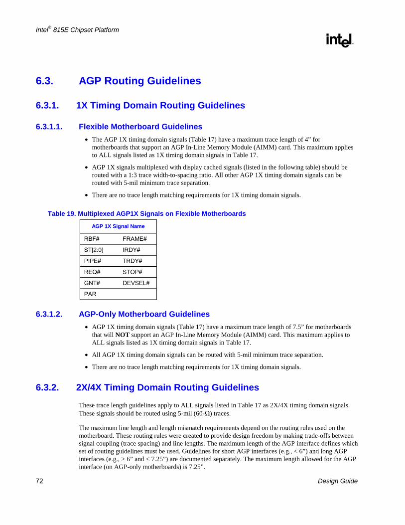
Intel® 815E Chipset Platform
R
72 Design Guide
6.3. AGP Routing Guidelines
6.3.1. 1X Timing Domain Routing Guidelines
6.3.1.1. Flexible Motherboard Guidelines • The AGP 1X timing domain signals (Table 17) have a maximum trace length of 4” for
motherboards that support an AGP In-Line Memory Module (AIMM) card. This maximum applies to ALL signals listed as 1X timing domain signals in Table 17.
• AGP 1X signals multiplexed with display cached signals (listed in the following table) should be routed with a 1:3 trace width-to-spacing ratio. All other AGP 1X timing domain signals can be routed with 5-mil minimum trace separation.
• There are no trace length matching requirements for 1X timing domain signals.
Table 19. Multiplexed AGP1X Signals on Flexible Motherboards
AGP 1X Signal Name
RBF# FRAME#
ST[2:0] IRDY#
PIPE# TRDY#
REQ# STOP#
GNT# DEVSEL#
PAR
6.3.1.2. AGP-Only Motherboard Guidelines • AGP 1X timing domain signals (Table 17) have a maximum trace length of 7.5” for motherboards
that will NOT support an AGP In-Line Memory Module (AIMM) card. This maximum applies to ALL signals listed as 1X timing domain signals in Table 17.
• All AGP 1X timing domain signals can be routed with 5-mil minimum trace separation.
• There are no trace length matching requirements for 1X timing domain signals.
6.3.2. 2X/4X Timing Domain Routing Guidelines
These trace length guidelines apply to ALL signals listed in Table 17 as 2X/4X timing domain signals. These signals should be routed using 5-mil (60-Ω) traces.
The maximum line length and length mismatch requirements depend on the routing rules used on the motherboard. These routing rules were created to provide design freedom by making trade-offs between signal coupling (trace spacing) and line lengths. The maximum length of the AGP interface defines which set of routing guidelines must be used. Guidelines for short AGP interfaces (e.g., < 6”) and long AGP interfaces (e.g., > 6” and < 7.25”) are documented separately. The maximum length allowed for the AGP interface (on AGP-only motherboards) is 7.25”.
Intel® 815E Chipset Platform
R
Design Guide 73
6.3.2.1. Flexible Motherboard Guidelines • For motherboards that support either an AGP card or an AIMM card in the AGP slot, the maximum
length of AGP 2X/4X timing domain signals is 4”.
• 1:3 trace width to spacing is required for AGP 2X/4X signal traces.
• AGP 2X/4X signals must be matched with their associated strobe (as outlined in Table 17), within ±0.5”.
For example, if a set of strobe signals (e.g., AD_STB0 and AD_STB0#) are 3.7” long, the data signals associated with those strobe signals (e.g., AD[15:0] and C/BE[2:0]#) can be 3.2” to 4” long (since there is a 4” max. length). Another strobe set (e.g., SB_STB and SB_STB#) could be 3.1” long, so that the associated data signals (e.g., SBA[7:0]) can be 2.6” to 3.6” long.
The strobe signals (AD_STB0, AD_STB0#, AD_STB1, AD_STB1#, SB_STB, and SB_STB#) act as clocks on the source-synchronous AGP interface. Therefore, special care must be taken when routing these signals. Since each strobe pair is truly a differential pair, the pair should be routed together (e.g., AD_STB0 and AD_STB0# should be routed next to each other). The two strobes in a strobe pair should be routed using 5-mil traces with at least 15 mils of space (1:3) between them. This pair should be separated from the rest of the AGP signals (and all other signals) by at least 20 mils (1:4). The strobe pair must be length-matched to less than ±0.1”. (That is, a strobe and its complement must be the same length within 0.1”.)
Figure 33. AGP 2X/4X Routing Example for Interfaces < 6” and AIMM/AGP Solutions
2X/4X signal
2X/4X signal
AGP STB#
AGP STB
2X/4X signal
2X/4X signal
15 mils
15 mils
15 mils
20 mils
20 mils
5-mil trace
5-mil trace
5-mil trace
5-mil trace
5-mil trace
2X/4X signal
2X/4X signal
AGP STB#
AGP STB
2X/4X signal
2X/4X signal
STB/STB# length
Associated AGP 2X/4X data signal length
Min. Max.0.5" 0.5"
AGP_2x-4x_routing
Intel® 815E Chipset Platform
R
74 Design Guide
6.3.2.2. AGP-Only Motherboard Guidelines
For motherboards that will not support an AIMM card populated in the AGP slot, the maximum AGP 2X/4X signal trace length is 7.25”. However, there are different guidelines for AGP interfaces shorter than 6” (e.g., all AGP 2X/4X signals are shorter than 6”) and those longer than 6” but shorter than the 7.25” maximum.
AGP Interfaces Shorter Than 6” The following guidelines are for designs that require less than 6” between the AGP connector and the GMCH:
• 1:3 trace width-to-spacing is required for AGP 2X/4X timing domain signal traces. • AGP 2X/4X signals must be matched with their associated strobe (as outlined in Table 17), within
±0.5”.
For example, if a set of strobe signals (e.g., AD_STB0 and AD_STB0#) are 5.3” long, the data signals associated with those strobe signals (e.g., AD[15:0] and C/BE[2:0]#) can be 4.8” to 5.8” long. Another strobe set (e.g., SB_STB and SB_STB#) could be 4.2” long, and the data signals associated with those strobe signals (e.g., SBA[7:0]) could be 3.7” to 4.7” long.
The strobe signals (AD_STB0, AD_STB0#, AD_STB1, AD_STB1#, SB_STB, and SB_STB#) act as clocks on the source-synchronous AGP interface. Therefore, special care must be taken when routing these signals. Because each strobe pair is truly a differential pair, the pair should be routed together (e.g., AD_STB0 and AD_STB0# should be routed next to each other). The two strobes in a strobe pair should be routed on 5-mil traces with at least 15 mils of space (1:3) between them. This pair should be separated from the rest of the AGP signals (and all other signals) by at least 20 mils (1:4). The strobe pair must be length-matched to less than ±0.1”. (That is, a strobe and its complement must be the same length, within 0.1”.) Refer to Table 17 for an illustration of these requirements.
AGP Interfaces Longer Than 6” Since longer lines have more cross-talk, they require wider spacing between traces to reduce the skew. The following guidelines are for designs that require more than 6” (but less than the 7.25” max.) between the AGP connector and the GMCH:
• 1:4 trace width-to-spacing is required for AGP 2X/4X timing domain signal traces. • AGP 2X/4X signals must be matched with their associated strobe (as outlined in Table 17), within
±0.125”.
For example, if a set of strobe signals (e.g., AD_STB0 and AD_STB0#) are 6.5” long, the data signals associated with those strobe signals (e.g., AD[15:0] and C/BE[2:0]#) can be 6.475” to 6.625” long. Another strobe set (e.g., SB_STB and SB_STB#) could be 6.2” long, and the data signals associated with those strobe signals (e.g., SBA[7:0]) could be 6.075” to 6.325” long.
The strobe signals (AD_STB0, AD_STB0#, AD_STB1, AD_STB1#, SB_STB, and SB_STB#) act as clocks on the source-synchronous AGP interface. Therefore, special care must be taken when routing these signals. Because each strobe pair is truly a differential pair, the pair should be routed together (e.g., AD_STB0 and AD_STB0# should be routed next to each other). The two strobes in a strobe pair should be routed on 5-mil traces with at least 20 mils of space (1:4) between them. This pair should be separated from the rest of the AGP signals (and all other signals) by at least 20 mils (1:4). The strobe pair must be length-matched to less than ±0.1”. (i.e., a strobe and its complement must be the same length, within 0.1”.)

Intel® 815E Chipset Platform
R
Design Guide 75
6.3.3. AGP Routing Guideline Considerations and Summary
This section applies to all AGP signals in any motherboard support configuration (e.g., “flexible” or “AGP only”):
• The 2X/4X timing domain signals can be routed with 5-mil spacing when breaking out of the GMCH. The routing must widen to the documented requirements within 0.3” of the GMCH package.
• When matching trace lengths for the AGP 4X interface, all traces should be matched from the ball of the GMCH to the pin on the AGP connector. It is not necessary to compensate for the length of the AGP signals on the GMCH package.
• Reduce line length mismatch to ensure added margin. The trace length mismatch for all signals within a signal group should be as close as possible to zero, to provide timing margin.
• To reduce trace-to-trace coupling (i.e., cross-talk), separate the traces as much as possible.
• All signals in a signal group should be routed on the same layer.
• The trace length and trace spacing requirements must not be violated by any signal.
Table 20. AGP 2.0 Routing Summary
Signal Maximum Length
Trace Spacing (5-Mil Traces)
Length Mismatch Relative To Notes
1X Timing Domain
7.5 4 5 mils No requirement
N/A None
2X/4X Timing Domain Set 1
7.25 4 20 mils ±0.125 AD_STB0 and AD_STB0#
AD_STB0 and AD_STB0# must be the same length.
2X/4X Timing Domain Set 2
7.25 4 20 mils ±0.125 AD_STB1 and AD_STB1#
AD_STB1 and AD_STB1# must be the same length.
2X/4X Timing Domain Set 3
7.254 20 mils ±0.125 SB_STB and SB_STB#
SB_STB and SB_STB# must be the same length.
2X/4X Timing Domain Set 1
6 3 15 mils1 ±0.5 AD_STB0 and AD_STB0#
AD_STB0 and AD_STB0# must be the same length.
2X/4X Timing Domain Set 2
63 15 mils1 ±0.5 AD_STB1 and AD_STB1#
AD_STB1 and AD_STB1# must be the same length.
2X/4X Timing Domain Set 3
63 15 mils1 ±0.5 SB_STB and SB_STB#
SB_STB and SB_STB# must be the same length.
NOTES: 1. Each strobe pair must be separated from other signals by at least 20 mils. 2. These guidelines apply to board stack-ups with 15% impedance tolerance. 3. 4 is the maximum length for flexible motherboards. 4. Solution valid for AGP-only motherboards

Intel® 815E Chipset Platform
R
76 Design Guide
6.3.4. AGP Clock Routing
The maximum total AGP clock skew, between the GMCH and the graphics component, is 1 ns for all data transfer modes. This 1 ns includes skew and jitter that originates on the motherboard, add-in card, and clock synthesizer. Clock skew must be evaluated not only at a single threshold voltage, but at all points on a clock edge that falls within in the switching range. The 1-ns skew budget is divided such that the motherboard is allotted 0.9 ns of clock skew. (The motherboard designer shall determine how the 0.9 ns is allocated between the board and the synthesizer.)
For the Intel® 815E chipset’s platform AGP clock routing guidelines, refer to Section 11.3.
6.3.5. AGP Signal Noise Decoupling Guidelines
The following routing guidelines are recommended for an optimal system design. The main focus of these guidelines is to minimize signal integrity problems on the AGP interface of the GMCH. The following guidelines are not intended to replace thorough system validation of Intel® 815E chipset-based products:
• A minimum of six 0.01-µF capacitors are required and must be as close as possible to the GMCH. These should be placed within 70 mils of the outer row of balls on the GMCH for VDDQ decoupling. The closer the placement, the better.
• The designer should evenly distribute the placement of decoupling capacitors within the AGP interface signal field.
• It is recommended that the designer use a low-ESL ceramic capacitor, such as a 0603 body-type X7R dielectric
• To add the decoupling capacitors within 70 mils of the GMCH and/or close to the vias, the trace spacing may be reduced as the traces go around each capacitor. The narrowing of the space between traces should be minimal and for as short a distance as possible (1” max.).
• In addition to the minimum decoupling capacitors, the designer should place bypass capacitors at vias that transition the AGP signal from one reference signal plane to another. In a typical four-layer PCB design, the signals transition from one side of the board to the other. One extra 0.01-µF capacitor is required per 10 vias. The capacitor should be placed as close as possible to the center of the via field.
The designer should ensure that the AGP connector is well decoupled, as described in the Rev. 1.0 AGP Design Guide, Section 1.5.3.3.

Intel® 815E Chipset Platform
R
Design Guide 77
Figure 34. AGP Decoupling Capacitor Placement Example
NOTES:
1. This figure is for example purposes only. It does not necessarily represent complete and correct routing for this interface.
6.3.6. AGP Routing Ground Reference
It is strongly recommended that, at a minimum, the following critical signals be referenced to ground from the GMCH to an AGP connector (or to an AGP video controller if implemented as a “down” solution on an AGP-only motherboard), using a minimum number of vias on each net: AD_STB0, AD_STB0#, AD_STB1, AD_STB1#, SB_STB, SB_STB#, G_GTRY#, G_IRDY#, G_GNT#, and ST[2:0].
In addition to the minimum signal set listed previously, it is strongly recommended that half of all AGP signals be reference to ground, depending on board layout. In an ideal design, the entire AGP interface signal field would be referenced to ground. This recommendation is not specific to any particular PCB stack-up, but should be applied to all Intel® 815E chipset designs.
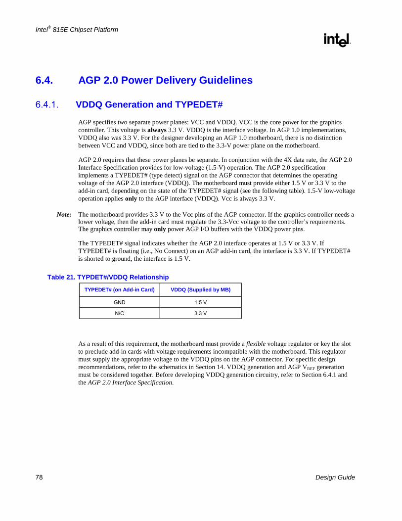
Intel® 815E Chipset Platform
R
78 Design Guide
6.4. AGP 2.0 Power Delivery Guidelines
6.4.1. VDDQ Generation and TYPEDET#
AGP specifies two separate power planes: VCC and VDDQ. VCC is the core power for the graphics controller. This voltage is always 3.3 V. VDDQ is the interface voltage. In AGP 1.0 implementations, VDDQ also was 3.3 V. For the designer developing an AGP 1.0 motherboard, there is no distinction between VCC and VDDQ, since both are tied to the 3.3-V power plane on the motherboard.
AGP 2.0 requires that these power planes be separate. In conjunction with the 4X data rate, the AGP 2.0 Interface Specification provides for low-voltage (1.5-V) operation. The AGP 2.0 specification implements a TYPEDET# (type detect) signal on the AGP connector that determines the operating voltage of the AGP 2.0 interface (VDDQ). The motherboard must provide either 1.5 V or 3.3 V to the add-in card, depending on the state of the TYPEDET# signal (see the following table). 1.5-V low-voltage operation applies only to the AGP interface (VDDQ). Vcc is always 3.3 V.
Note: The motherboard provides 3.3 V to the Vcc pins of the AGP connector. If the graphics controller needs a lower voltage, then the add-in card must regulate the 3.3-Vcc voltage to the controller’s requirements. The graphics controller may only power AGP I/O buffers with the VDDQ power pins.
The TYPEDET# signal indicates whether the AGP 2.0 interface operates at 1.5 V or 3.3 V. If TYPEDET# is floating (i.e., No Connect) on an AGP add-in card, the interface is 3.3 V. If TYPEDET# is shorted to ground, the interface is 1.5 V.
Table 21. TYPDET#/VDDQ Relationship
TYPEDET# (on Add-in Card) VDDQ (Supplied by MB)
GND 1.5 V
N/C 3.3 V
As a result of this requirement, the motherboard must provide a flexible voltage regulator or key the slot to preclude add-in cards with voltage requirements incompatible with the motherboard. This regulator must supply the appropriate voltage to the VDDQ pins on the AGP connector. For specific design recommendations, refer to the schematics in Section 14. VDDQ generation and AGP VREF generation must be considered together. Before developing VDDQ generation circuitry, refer to Section 6.4.1 and the AGP 2.0 Interface Specification.
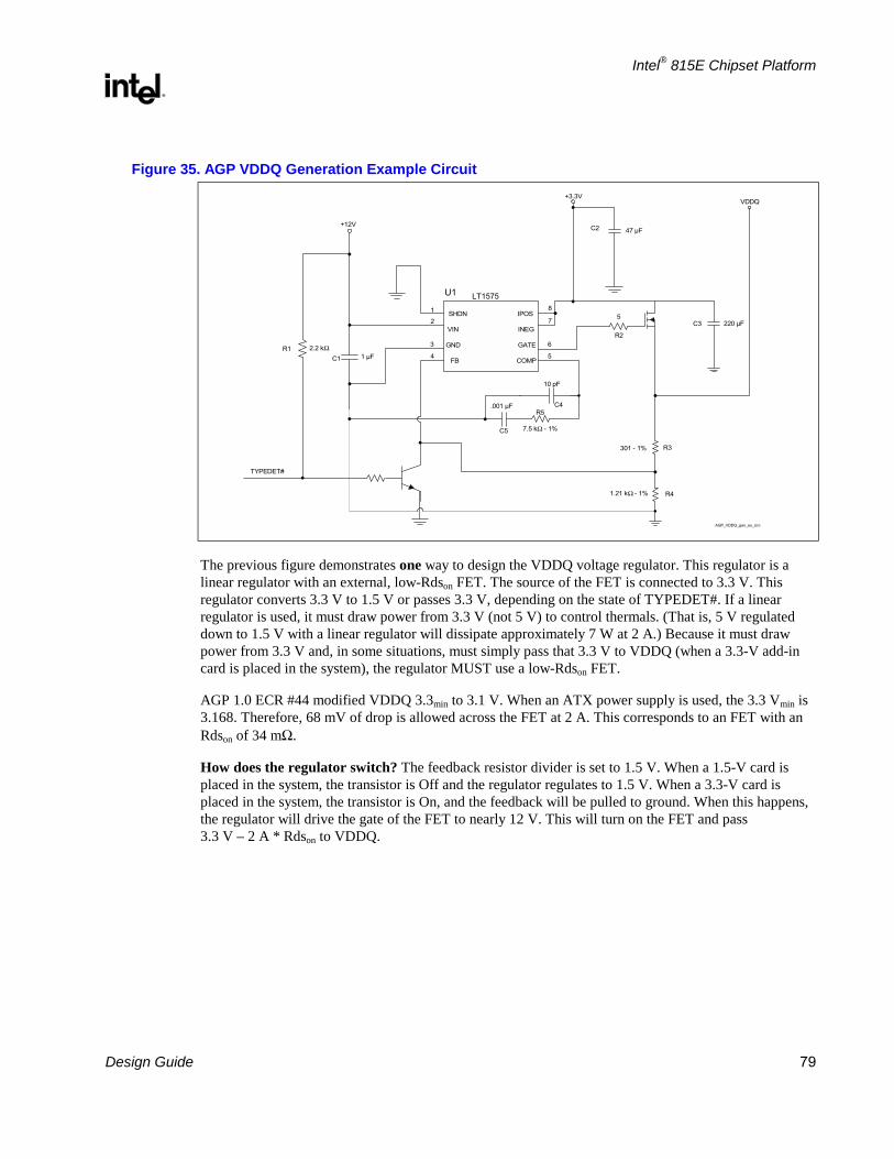
Intel® 815E Chipset Platform
R
Design Guide 79
Figure 35. AGP VDDQ Generation Example Circuit
SHDN IPOS
VIN INEG
GND GATE
FB COMPC1 2.2 kΩ
10 pF
C2
5
R3
R4
C3
+12V
+3.3VVDDQ
R1 1 µF
TYPEDET#
U1 LT15751
2
3
4
8
7
6
5
C5
R5C4
R2
301 - 1%
1.21 kΩ - 1%
47 µF
220 µF
AGP_VDDQ_gen_ex_circ
.001 µF
7.5 kΩ - 1%
The previous figure demonstrates one way to design the VDDQ voltage regulator. This regulator is a linear regulator with an external, low-Rdson FET. The source of the FET is connected to 3.3 V. This regulator converts 3.3 V to 1.5 V or passes 3.3 V, depending on the state of TYPEDET#. If a linear regulator is used, it must draw power from 3.3 V (not 5 V) to control thermals. (That is, 5 V regulated down to 1.5 V with a linear regulator will dissipate approximately 7 W at 2 A.) Because it must draw power from 3.3 V and, in some situations, must simply pass that 3.3 V to VDDQ (when a 3.3-V add-in card is placed in the system), the regulator MUST use a low-Rdson FET.
AGP 1.0 ECR #44 modified VDDQ 3.3min to 3.1 V. When an ATX power supply is used, the 3.3 Vmin is 3.168. Therefore, 68 mV of drop is allowed across the FET at 2 A. This corresponds to an FET with an Rdson of 34 mΩ.
How does the regulator switch? The feedback resistor divider is set to 1.5 V. When a 1.5-V card is placed in the system, the transistor is Off and the regulator regulates to 1.5 V. When a 3.3-V card is placed in the system, the transistor is On, and the feedback will be pulled to ground. When this happens, the regulator will drive the gate of the FET to nearly 12 V. This will turn on the FET and pass 3.3 V – 2 A * Rdson to VDDQ.

Intel® 815E Chipset Platform
R
80 Design Guide
6.4.2. VREF Generation for AGP 2.0 (2X and 4X)
VREF generation for AGP 2.0 is different, depending on the AGP card type used. 3.3-V AGP cards generate VREF locally. That is, they have a resistor divider on the card that divides VDDQ down to VREF (see the following figure). To account for potential differences between VDDQ and GND at the GMCH and graphics controller, 1.5-V cards use source-generated VREF. That is, the VREF signal is generated at the graphics controller and sent to the GMCH, and another VREF is generated at the GMCH and sent to the graphics controller (see the following figure)
Both the graphics controller and the GMCH must generate VREF and distribute it through the connector (1.5-V add-in cards only). The following two pins defined on the AGP 2.0 universal connector allow this VREF passing:
• VrefGC - VREF from the graphics controller to the chipset
• VrefCG - VREF from the chipset to the graphics controller
To preserve the common-mode relationship between the VREF and data signals, the routing of the two VREF signals must be matched in length to the strobe lines, within 0.5” on the motherboard and within 0.25” on the add-in card.
The voltage divider networks consist of AC and DC elements, as shown in the figure.
The VREF divider network should be placed as close as practical to the AGP interface, to get the benefit of the common-mode power supply effects. However, the trace spacing around the VREF signals must be a minimum of 25 mils to reduce cross-talk and maintain signal integrity.
During 3.3-V AGP 2.0 operation, VREF must be 0.4 VDDQ. However, during 1.5-V AGP 2.0 operation, VREF must be 0.5 VDDQ. This requires a flexible voltage divider for VREF. Various methods of accomplishing this exist, and one such example is shown in the following figure.
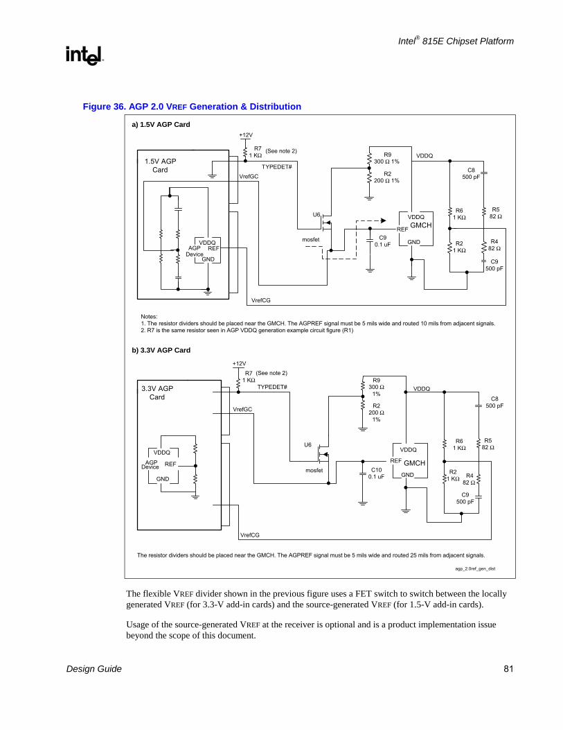
Intel® 815E Chipset Platform
R
Design Guide 81
Figure 36. AGP 2.0 VREF Generation & Distribution
C8500 pF
AGPDevice
1.5V AGPCard
VDDQ
GND
R9 300 Ω 1%
R2 200 Ω 1%
C90.1 uF
VDDQ
REF
GND
GMCH
C8500 pF
REF
U6
mosfet
R71 KΩ
+12V
TYPEDET#
VrefCG
VrefGC
VDDQ
Notes:1. The resistor dividers should be placed near the GMCH. The AGPREF signal must be 5 mils wide and routed 10 mils from adjacent signals.2. R7 is the same resistor seen in AGP VDDQ generation example circuit figure (R1)
AGPDevice
3.3V AGPCard
VDDQ
GNDC10
0.1 uF
VDDQ
REF
GND
GMCH
R61 KΩ
R21 KΩ
R582 Ω
R482 Ω
REF
U6
mosfet
+12V
TYPEDET#
VrefCG
VrefGC
VDDQ
The resistor dividers should be placed near the GMCH. The AGPREF signal must be 5 mils wide and routed 25 mils from adjacent signals.
C9500 pF
R9300 Ω
1%
R2200 Ω
1%
agp_2.0ref_gen_dist
b) 3.3V AGP Card
a) 1.5V AGP Card
R61 KΩ
R582 Ω
R21 KΩ
R482 Ω
C9500 pF
(See note 2)
R71 KΩ
(See note 2)
The flexible VREF divider shown in the previous figure uses a FET switch to switch between the locally generated VREF (for 3.3-V add-in cards) and the source-generated VREF (for 1.5-V add-in cards).
Usage of the source-generated VREF at the receiver is optional and is a product implementation issue beyond the scope of this document.

Intel® 815E Chipset Platform
R
82 Design Guide
6.5. Additional AGP Design Guidelines
6.5.1. Compensation
The GMCH AGP interface supports resistive buffer compensation (RCOMP). Tie the GRCOMP pin to a 40-Ω, 2% (or 39-Ω, 1%) pull-down resistor (to ground) via a 10-mil-wide, very short (<0.5”) trace.
6.5.2. AGP Pull-ups
AGP control signals require pull-up resistors to VDDQ on the motherboard, to ensure that they contain stable values when no agent is actively driving the bus. The signals requiring pull-up resistors are as follows:
1X Timing Domain Signals:
• FRAME# • TRDY# • IRDY# • DEVSEL# • STOP# • SERR# • PERR# • RBF# • PIPE# • REQ# • WBF# • GNT# • ST[2:0]
It is critical that these signals be pulled up to VDDQ, not 3.3 V.
The trace stub to the pull-up resistor on 1X timing domain signals should be kept shorter than 0.5” to avoid signal reflections from the stub.
The strobe signals require pull-up/pull-downs on the motherboard to ensure they contain stable values when no agent is driving the bus.
Note: INTA# and INTB# should be pulled to 3.3 V, not VDDQ.
2X/4X Timing Domain Signals:
• AD_STB[1:0] (pull-up to VDDQ) • SB_STB (pull up to VDDQ) • AD_STB[1:0]# (pull down to ground) • SB_STB# (pull down to ground)
The trace stub to the pull-up/pull-down resistor on 2X/4X timing domain signals should be kept shorter than 0.1” to avoid signal reflections from the stub.

Intel® 815E Chipset Platform
R
Design Guide 83
The pull-up/pull-down resistor value requirements are Rmin = 4 kΩ and Rmax = 16 kΩ. The recommended AGP pull-up/pull-down resistor value is 8.2 kΩ.
6.5.2.1. AGP Signal Voltage Tolerance List
The following signals on the AGP interface are 3.3-V tolerant during 1.5-V operation:
• PME# • INTA# • INTB# • GPERR# • GSERR# • CLK • RST
The following signals on the AGP interface are 5-V tolerant (see USB specification):
• USB+ • USB- • OVRCNT#
The following signal is a special AGP signal. It is either GROUNDED or NO CONNECTED on an AGP card.
• TYPEDET#
ALL OTHER SIGNALS ON THE AGP INTERFACE ARE IN THE VDDQ GROUP. THEY ARE NOT 3.3-V TOLERANT DURING 1.5-V AGP OPERATION!
6.6. Motherboard / Add-in Card Interoperability There are three AGP connectors: 3.3-V AGP connector, 1.5-V AGP connector, and Universal AGP connector. To maximize add-in flexibility, it is highly advisable to implement the universal connector in an Intel® 815E chipset-based system. All add-in cards are either 3.3-V or 1.5-V cards. 4X transfers at 3.3 V are not allowed due to timings.
Table 22. Connector/Add-in Card Interoperability
1.5-V Connector 3.3-V Connector Universal Connector
1.5-V card NO
3.3-V card NO
Table 23. Voltage/Data Rate Interoperability
1X 2X 4X
1.5 V VDDQ
3.3 V VDDQ NO

Intel® 815E Chipset Platform
R
84 Design Guide
6.7. AGP / Display Cache Shared Interface As described earlier, the AGP and display cache interfaces of the Intel® 815E chipset are multiplexed or shared. In other words, the same component pins (balls) are used for both interfaces, although obviously only one interface can be supported at any given time. As a result, almost all display cache interface signals are mapped onto the new AGP interface. The Intel® 815E chipset can be configured in either AGP mode or Graphics mode. In the AGP mode, the interface supports a full AGP 4X interface. In the Graphics mode, the interface becomes a display cache interface similar to the Intel® 810E chipset. Note, however, that in the Graphics mode, the display cache is optional. There do not have to be any SDRAM devices connected to the interface. The only dedicated display cache signals are OCLK and RCLK, which need not connect directly to the SDRAM devices. These are not mapped onto existing AGP signals.
6.7.1. AIMM Card Considerations
To support the fullest flexibility, the display cache exists on an add-in card (AGP In-Line Memory Module, or AIMM) that complies with the AGP connector form factor. If the motherboard designer follows the flexible routing guidelines for the AGP interface detailed in previous sections, the customer can choose to populate the AGP slot in an Intel® 815E chipset-based system with either an AGP graphics card, with an AIMM card to enable the highest-possible internal graphics performance, or with nothing to get the lowest-cost internal graphics solution. Some of the AIMM/Intel® 815E chipset interfacing implications are as follows. For a complete description of the AIMM card design, refer to the AGP Inline Memory Module Specification available from Intel.
• A strap is required to determine which frequency to select for display cache operation. This is the L_FSEL pin of the GMCH. The AIMM card will pull this signal up or down as appropriate to communicate to the Intel® 815E chipset the appropriate operating frequency. The Intel® 815E chipset will sample this pin on the deasserting edge of reset.
• Since current SDRAM technology is always 3.3 V rather than the 1.5-V option also supported by AGP, the AIMM card should set the TYPEDET# signal correctly to indicate that it requires a 3.3-V power supply. Furthermore, the AIMM card should have only the 3.3-V key and not the 1.5-V key, thereby preventing it from being inserted into a 1.5-V-only connector.
• The pad buffers on the chip will be the normal AGP buffers and will work for both interfaces.
• In internal graphics mode, the AGPREF signal, which is required for the AGP mode, should remain functional as a reference voltage for sampling 3.3-V LMD inputs. The voltage level on AGPREF should remain exactly the same as in the AGP mode, as opposed to the VCC/2 used for previous products.
6.7.1.1. AGP and AIMM Mechanical Considerations
The AIMM card will be designed with a notch on the PCB to go around the AGP universal retention mechanism. To guarantee that the AIMM card will meet all shock and vibration requirements of the system, the AGP universal retention mechanism will be required on all AGP sockets that are to support an AIMM card.
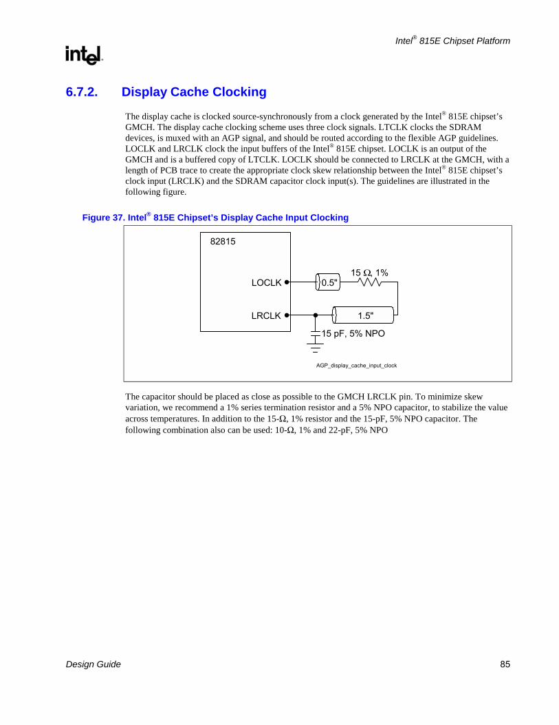
Intel® 815E Chipset Platform
R
Design Guide 85
6.7.2. Display Cache Clocking
The display cache is clocked source-synchronously from a clock generated by the Intel® 815E chipset’s GMCH. The display cache clocking scheme uses three clock signals. LTCLK clocks the SDRAM devices, is muxed with an AGP signal, and should be routed according to the flexible AGP guidelines. LOCLK and LRCLK clock the input buffers of the Intel® 815E chipset. LOCLK is an output of the GMCH and is a buffered copy of LTCLK. LOCLK should be connected to LRCLK at the GMCH, with a length of PCB trace to create the appropriate clock skew relationship between the Intel® 815E chipset’s clock input (LRCLK) and the SDRAM capacitor clock input(s). The guidelines are illustrated in the following figure.
Figure 37. Intel® 815E Chipset’s Display Cache Input Clocking
15 Ω, 1%
15 pF, 5% NPO
82815
LOCLK
LRCLK
0.5"
1.5"
AGP_display_cache_input_clock
The capacitor should be placed as close as possible to the GMCH LRCLK pin. To minimize skew variation, we recommend a 1% series termination resistor and a 5% NPO capacitor, to stabilize the value across temperatures. In addition to the 15-Ω, 1% resistor and the 15-pF, 5% NPO capacitor. The following combination also can be used: 10-Ω, 1% and 22-pF, 5% NPO

Intel® 815E Chipset Platform
R
86 Design Guide
This page intentionally left blank.

Intel® 815E Chipset Platform
R
Design Guide 87
7. Integrated Graphics Display Output
7.1. Analog RGB/CRT
7.1.1. RAMDAC/Display Interface
The following figure shows the interface of the RAMDAC analog current outputs with the display. Each DAC output is doubly terminated with a 75-Ω resistance. One 75-Ω resistance is from the DAC output to the board ground, and the other termination resistance exists within the display. The equivalent DC resistance at the output of each DAC output is 37.5 Ω. The output current of each DAC flows into this equivalent resistive load to produce a video voltage, without the need for external buffering. There is also an LC pi-filter that is used to reduce high-frequency glitches and noise and to reduce EMI. To maximize performance, the filter impedance, cable impedance, and load impedance should be the same. The LC pi-filter consists of two 3.3-pF capacitors and a ferrite bead with a 75-Ω impedance at 100 MHz. The LC pi-filter is designed to filter glitches produced by the RAMDAC, while maintaining adequate edge rates to support high-end display resolutions.
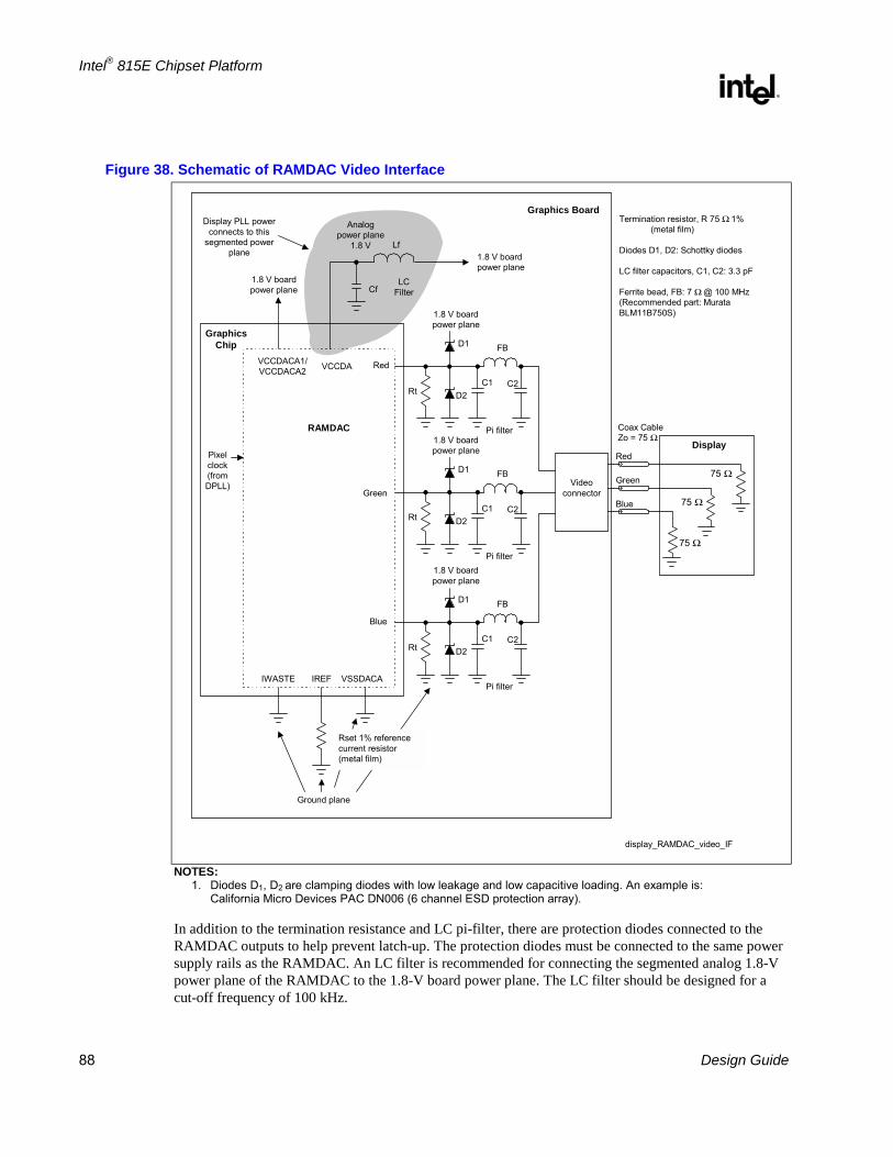
Intel® 815E Chipset Platform
R
88 Design Guide
Figure 38. Schematic of RAMDAC Video Interface
RAMDAC
VCCDACA1/VCCDACA2 VCCDA Red
GraphicsChip
Pixelclock(fromDPLL)
Cf
Lf
LCFilter
1.8 V boardpower plane
Display PLL powerconnects to this
segmented powerplane 1.8 V board
power plane
1.8 V boardpower plane
Rt D2
D1
C1 C2
FB
Pi filter1.8 V boardpower plane
Rt D2
D1
C1 C2
FB
Pi filter1.8 V boardpower plane
Rt D2
D1
C1 C2
FB
Pi filter
Green
Blue
VSSDACA
Analogpower plane
1.8 V
IREFIWASTE
Ground plane
Rset 1% referencecurrent resistor(metal film)
Videoconnector
Graphics Board
Red
Green
Blue
Coax CableZo = 75 Ω
75 Ω
75 Ω
75 Ω
Display
Termination resistor, R 75 Ω 1% (metal film)
Diodes D1, D2: Schottky diodes
LC filter capacitors, C1, C2: 3.3 pF
Ferrite bead, FB: 7 Ω @ 100 MHz(Recommended part: MurataBLM11B750S)
display_RAMDAC_video_IF NOTES:
1. Diodes D1, D2 are clamping diodes with low leakage and low capacitive loading. An example is: California Micro Devices PAC DN006 (6 channel ESD protection array).
In addition to the termination resistance and LC pi-filter, there are protection diodes connected to the RAMDAC outputs to help prevent latch-up. The protection diodes must be connected to the same power supply rails as the RAMDAC. An LC filter is recommended for connecting the segmented analog 1.8-V power plane of the RAMDAC to the 1.8-V board power plane. The LC filter should be designed for a cut-off frequency of 100 kHz.

Intel® 815E Chipset Platform
R
Design Guide 89
7.1.2. Reference Resistor (Rset) Calculation
The full-swing video output is designed to be 0.7 V, according to the VESA video standard. With an equivalent DC resistance of 37.5 Ω (two 75-Ω resistors in parallel; one 75-Ω termination on the board and one 75-Ω termination within the display), the full-scale output current of a RAMDAC channel is 0.7/37.5 Ω = 18.67 mA. Since the RAMDAC is an 8-bit current-steering DAC, this full-scale current is equivalent 255 I, where I is a unit current. Therefore, the unit current or LSB current of the DAC signals equals 73.2 µA. The reference circuitry generates a voltage across this Rset resistor equal to the bandgap voltage divided by three (i.e., 407.6 mV). The RAMDAC reference current generation circuitry is designed to generate a 32-I reference current using the reference voltage and the Rset value. To generate a 32-I reference current for the RAMDAC, the reference current setting resistor, Rset, is calculated from the following equation:
Rset = VREF / 32 I = 0.4076 V / 32 * 73.2 µA = 174 Ω
7.1.3. RAMDAC Board Design Guidelines
The following figure shows a general cross section of a typical four-layer board. The recommended RAMDAC routing for a four-layer board is such that the red, green, and blue video outputs are routed on the top (bottom) layer over (under) a solid ground plane to maximize the noise rejection characteristics of the video outputs. It is essential to prevent toggling signals from being routed next to the video output signals to the VGA connector. A 20-mil spacing between any video route and any other routes is recommended.
Figure 39. Cross-Sectional View of a Four-Layer Board
Board Cross Section
Boardcomponents
RAMDAC / PLL circuitry
Graphics chipOne solid, continuous
ground plane
Digital power plane
RAMDAC_board_xsec
Bottom of board Segmented analog powerplane for RAMDAC / PLL
Low-frequencysignal traces
Ground plane
Analog traces
Videoconnector
Top of boardAvoid clock routes orhigh-frequency routes inthe area of the RAMDACoutput signals andreference resistor.
Matching of the video routes (i.e., red, green, blue) from the RAMDAC to the VGA connector is also essential. The routing for these signals should be as similar as possible (i.e., same routing layer(s), same number of vias, same routing length, same bends and jogs).
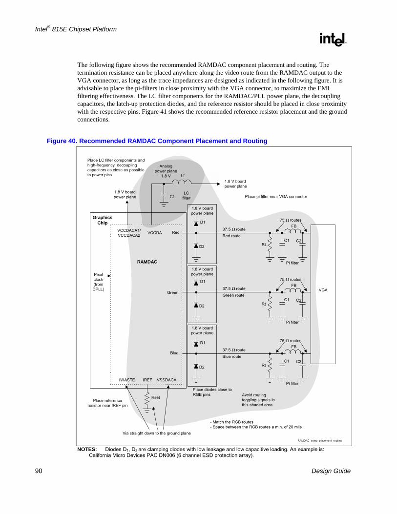
Intel® 815E Chipset Platform
R
90 Design Guide
The following figure shows the recommended RAMDAC component placement and routing. The termination resistance can be placed anywhere along the video route from the RAMDAC output to the VGA connector, as long as the trace impedances are designed as indicated in the following figure. It is advisable to place the pi-filters in close proximity with the VGA connector, to maximize the EMI filtering effectiveness. The LC filter components for the RAMDAC/PLL power plane, the decoupling capacitors, the latch-up protection diodes, and the reference resistor should be placed in close proximity with the respective pins. Figure 41 shows the recommended reference resistor placement and the ground connections.
Figure 40. Recommended RAMDAC Component Placement and Routing
RAMDAC
VCCDACA1/VCCDACA2 VCCDA Red
GraphicsChip
Pixelclock(fromDPLL)
Cf
Lf
LCfilter
1.8 V boardpower plane
Place LC filter components andhigh-frequency decouplingcapacitors as close as possibleto power pins
1.8 V boardpower plane
Green
Blue
VSSDACA
Analogpower plane
1.8 V
IREFIWASTE
Place referenceresistor near IREF pin
Rset
VGA
RAMDAC comp placement routing
1.8 V boardpower plane
RtD2
D1
C1 C2
FB
Pi filter
Red route37.5 Ω route
75 Ω routes
1.8 V boardpower plane
RtD2
D1
C1 C2
FB
Pi filter
Green route37.5 Ω route
75 Ω routes
1.8 V boardpower plane
RtD2
D1
C1 C2
FB
Pi filter
Blue route37.5 Ω route
75 Ω routes
Place diodes close toRGB pins Avoid routing
toggling signals inthis shaded area
Via straight down to the ground plane
- Match the RGB routes- Space between the RGB routes a min. of 20 mils
Place pi filter near VGA connector
NOTES: Diodes D1, D2 are clamping diodes with low leakage and low capacitive loading. An example is:
California Micro Devices PAC DN006 (6 channel ESD protection array).
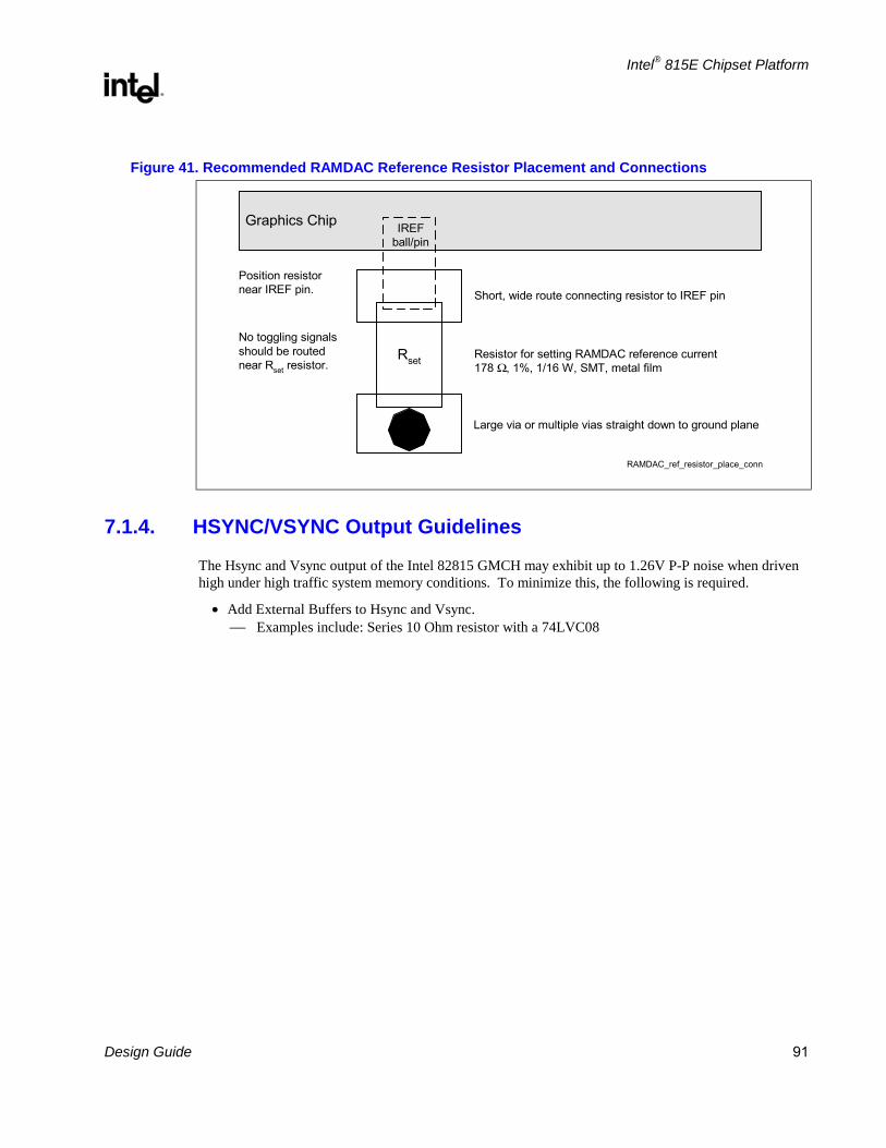
Intel® 815E Chipset Platform
R
Design Guide 91
Figure 41. Recommended RAMDAC Reference Resistor Placement and Connections
Graphics Chip IREFball/pin
Rset
Large via or multiple vias straight down to ground plane
Resistor for setting RAMDAC reference current178 Ω, 1%, 1/16 W, SMT, metal film
Short, wide route connecting resistor to IREF pin
Position resistornear IREF pin.
No toggling signalsshould be routednear Rset resistor.
RAMDAC_ref_resistor_place_conn
7.1.4. HSYNC/VSYNC Output Guidelines
The Hsync and Vsync output of the Intel 82815 GMCH may exhibit up to 1.26V P-P noise when driven high under high traffic system memory conditions. To minimize this, the following is required.
• Add External Buffers to Hsync and Vsync. Examples include: Series 10 Ohm resistor with a 74LVC08
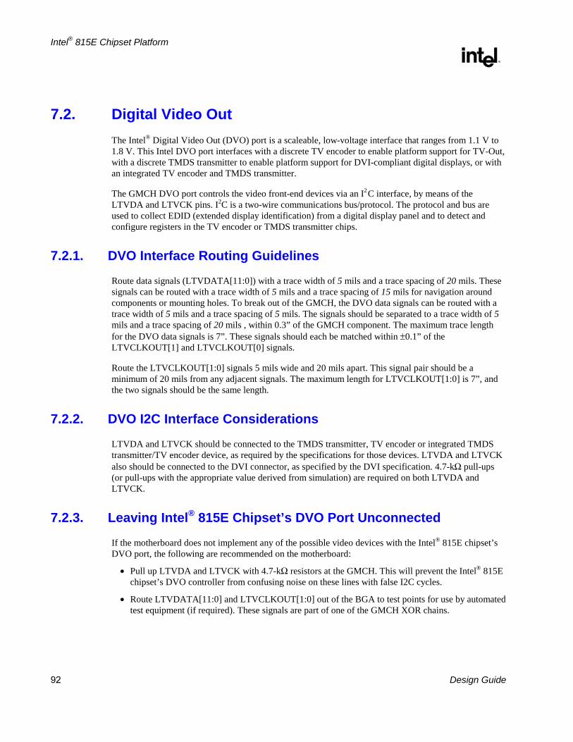
Intel® 815E Chipset Platform
R
92 Design Guide
7.2. Digital Video Out The Intel® Digital Video Out (DVO) port is a scaleable, low-voltage interface that ranges from 1.1 V to 1.8 V. This Intel DVO port interfaces with a discrete TV encoder to enable platform support for TV-Out, with a discrete TMDS transmitter to enable platform support for DVI-compliant digital displays, or with an integrated TV encoder and TMDS transmitter.
The GMCH DVO port controls the video front-end devices via an I2 C interface, by means of the LTVDA and LTVCK pins. I2C is a two-wire communications bus/protocol. The protocol and bus are used to collect EDID (extended display identification) from a digital display panel and to detect and configure registers in the TV encoder or TMDS transmitter chips.
7.2.1. DVO Interface Routing Guidelines
Route data signals (LTVDATA[11:0]) with a trace width of 5 mils and a trace spacing of 20 mils. These signals can be routed with a trace width of 5 mils and a trace spacing of 15 mils for navigation around components or mounting holes. To break out of the GMCH, the DVO data signals can be routed with a trace width of 5 mils and a trace spacing of 5 mils. The signals should be separated to a trace width of 5 mils and a trace spacing of 20 mils , within 0.3” of the GMCH component. The maximum trace length for the DVO data signals is 7”. These signals should each be matched within ±0.1” of the LTVCLKOUT[1] and LTVCLKOUT[0] signals.
Route the LTVCLKOUT[1:0] signals 5 mils wide and 20 mils apart. This signal pair should be a minimum of 20 mils from any adjacent signals. The maximum length for LTVCLKOUT[1:0] is 7”, and the two signals should be the same length.
7.2.2. DVO I2C Interface Considerations
LTVDA and LTVCK should be connected to the TMDS transmitter, TV encoder or integrated TMDS transmitter/TV encoder device, as required by the specifications for those devices. LTVDA and LTVCK also should be connected to the DVI connector, as specified by the DVI specification. 4.7-kΩ pull-ups (or pull-ups with the appropriate value derived from simulation) are required on both LTVDA and LTVCK.
7.2.3. Leaving Intel® 815E Chipset’s DVO Port Unconnected
If the motherboard does not implement any of the possible video devices with the Intel® 815E chipset’s DVO port, the following are recommended on the motherboard:
• Pull up LTVDA and LTVCK with 4.7-kΩ resistors at the GMCH. This will prevent the Intel® 815E chipset’s DVO controller from confusing noise on these lines with false I2C cycles.
• Route LTVDATA[11:0] and LTVCLKOUT[1:0] out of the BGA to test points for use by automated test equipment (if required). These signals are part of one of the GMCH XOR chains.

Intel® 815E Chipset Platform
R
Design Guide 93
8. Hub Interface The Intel® 815 chipset’s GMCH ball assignment and ICH2 ball assignment have been optimized to simplify hub interface routing. It is recommended that the hub interface signals be routed directly from the GMCH to the ICH2 on the top signal layer. Refer to the following figure.
The hub interface is divided into two signal groups: data signals and strobe signals.
• Data Signals: HL[10:0]
• Strobe Signals: HL_STB HL_STB#
Note: HL_STB/HL_STB# is a differential strobe pair.
No pull-ups or pull-downs are required on the hub interface. HL[11] on the ICH2 should be brought out to a test point for NAND Tree testing. Each signal should be routed such that it meets the guidelines documented for its signal group.
Figure 42. Hub Interface Signal Routing Example
ICH2 GMCH
Clocks
HL_STB
HL_STB#
HL[10:0]
CLK66 GCLK
HL11
hub_link_sig_routing
NAND treetest point
Intel® 815E Chipset Platform
R
94 Design Guide
8.1.1. Data Signals
Hub interface data signals should be routed with a trace width of 5 mils and a trace spacing of 20 mils. These signals can be routed with a trace width of 5 mils and a trace spacing of 15 mils for navigation around components or mounting holes. To break out of the GMCH and the ICH2, the hub interface data signals can be routed with a trace width of 5 mils and a trace spacing of 5 mils. The signals should be separated to a trace width of 5 mils and a trace spacing of 20 mils, within 0.3” of the GMCH/ICH2 components.
The maximum trace length for the hub interface data signals is 7”. These signals should each be matched within ±0.1” of the HL_STB and HL_STB# signals.
8.1.2. Strobe Signals
Due to their differential nature, the hub interface strobe signals should be 5 mils wide and routed 20 mils apart. This strobe pair should be a minimum of 20 mils from any adjacent signals. The maximum length for the strobe signals is 7”, and the two strobes should be the same length. Additionally, the trace length for each data signal should be matched to the trace length of the strobes, within ±0.1”.
8.1.3. HREF Generation/Distribution
HREF, the hub interface reference voltage, is 0.5 * 1.85 V = 0.92 V ± 2%. It can be generated using a single HREF divider or locally generated dividers (as shown in the following two figures). The resistors should be equal in value and rated at 1% tolerance, to maintain 2% tolerance on 0.92 V. The values of these resistors must be chosen to ensure that the reference voltage tolerance is maintained over the entire input leakage specification. The recommended range for the resistor value is from a minimum of 100 Ω to a maximum of 1 kΩ (300 Ω shown in example).
The single HREF divider should not be located more than 4” away from either GMCH or ICH2. If the single HREF divider is located more than 4" away, then the locally generated hub interface reference dividers should be used instead.
The reference voltage generated by a single HREF divider should be bypassed to ground at each component with a 0.01-µF capacitor located close to the component HREF pin. If the reference voltage is generated locally, the bypass capacitor must be close to the component HREF pin.
8.1.4. Compensation
Independent Hub interface compensation resistors are used by the Intel® 815 chipset’s GMCH and the ICH2 to adjust buffer characteristics to specific board characteristics. Refer to the Intel® 815 Chipset Family: 82815 Graphics and Memory Controller Hub (GMCH) Datasheet and the Intel® 82801BA I/O Controller Hub 2 (ICH2) Datasheet for details on compensation. The resistive Compensation (RCOMP) guidelines are as follows:
RCOMP: Tie the HLCOMP pin of each component to a 40-Ω, 1% or 2% pull-up resistor (to 1.8 V) via a 10-mil-wide, 0.5” trace (targeted at a nominal trace impedance of 40 Ω). The GMCH and ICH2 each requires its own RCOMP resistor.

Intel® 815E Chipset Platform
R
Design Guide 95
Figure 43. Single Hub Interface Reference Divider Circuit
HUBREF HUBREF
GMCH ICH2
hub_IF_ref_div_1
300 Ω
1.85 V
300 Ω0.01 µF 0.01 µF
0.1 µF
Figure 44. Locally Generated Hub Interface Reference Dividers
HUBREF HUBREF
GMCH ICH2
hub_IF_ref_
300 Ω
1.85 V
300 Ω 0.1 µF
300 Ω
1.85 V
300 Ω0.1 µF

Intel® 815E Chipset Platform
R
96 Design Guide
This page intentionally left blank.

Intel® 815E Chipset Platform
R
Design Guide 97
9. ICH2
9.1. Decoupling The ICH2 is capable of generating large current swings when switching between logic High and logic Low. This condition could cause the component voltage rails to drop below specified limits. To avoid this type of situation, ensure that the appropriate amount of bulk capacitance is added in parallel to the voltage input pins. It is recommended that the developer use the amount of decoupling capacitors specified in the following table to ensure that the component maintains stable supply voltages. The capacitors should be placed as close as possible to the package, without exceeding 400 mils (100–300 mils nominal). Note: Routing space around the ICH2 is tight. A few decoupling caps may be placed more than 300 mils away from the package. System designers should simulate the board to ensure that the correct amount decoupling is implemented. Refer to the following figure for a layout example. It is recommended that, for prototype board designs, the designer include pads for extra power plane decoupling caps.
Table 24. Decoupling Capacitor Recommendation
Power Plane/Pins Decoupling Capacitors Capacitor Value
3.3-V core 6 .1 µF
3.3-V standby 1 .1 µF
Processor interface (1.3 ~ 2.5 V) 1 .1 µF
1.8-V core 2 .1 µF
1.8-V standby 1 .1 µF
5-V reference 1 .1 µF
5-V reference standby 1 .1 µF

Intel® 815E Chipset Platform
R
98 Design Guide
Figure 45. ICH2 Decoupling Capacitor Layout
3.3V Core1.8V Core
1.8V Standby
3.3V Standby
3.3V Core1.8V Standby
5V Refdecouple_cap_layout
9.2. 1.8V/3.3V Power Sequencing The ICH2 has two pairs of associated 1.8V and 3.3V supplies. These are Vcc1_8, Vcc3_3 and VccSus1_8, VccSus3_3. These pairs are assumed to power up and power down together. The difference between the two associated supplies must never be greater than 2.0V. The 1.8V supply may come up before the 3.3V supply without violating this rule (though this is generally not practical in a desktop environment, since the 1.8V supply is typically derived from the 3.3V supply by means of a linear regulator).
One serious consequence of violation of this "2V Rule" is electrical overstress of oxide layers, resulting in component damage.
The majority of the ICH2 I/O buffers are driven by the 3.3V supplies, but are controlled by logic that is powered by the 1.8V supplies. Thus, another consequence of faulty power sequencing arises if the 3.3V supply comes up first. In this case the I/O buffers will be in an undefined state until the 1.8V logic is powered up. Some signals that are defined as "Input-only" actually have output buffers that are normally disabled, and the ICH2 may unexpectedly drive these signals if the 3.3V supply is active while the 1.8V supply is not.

Intel® 815E Chipset Platform
R
Design Guide 99
The figure below shows an example power-on sequencing circuit that ensures the “2V Rule” is obeyed. This circuit uses a NPN (Q2) and PNP (Q1) transistor to ensure the 1.8V supply tracks the 3.3V supply. The NPN transistor controls the current through PNP from the 3.3V supply into the 1.8V power plane by varying the voltage at the base of the PNP transistor. By connecting the emitter of the NPN transistor to the 1.8V plane, current will not flow from the 3.3V supply into 1.8V plane when the 1.8V plane reaches 1.8V.
Figure 46. Example 1.8V/3.3V Power Sequencing Circuit
Q1 PNP
Q2 NPN
220
220
470
+3.3V +1.8V
When analyzing systems that may be "marginally compliant" to the 2V Rule, pay close attention to the behavior of the ICH2's RSMRST# and PWROK signals, since these signals control internal isolation logic between the various power planes:
• RSMRST# controls isolation between the RTC well and the Resume wells.
• PWROK controls isolation between the Resume wells and Main wells
If one of these signals goes high while one of its associated power planes is active and the other is not, a leakage path will exist between the active and inactive power wells. This could result in high, possibly damaging, internal currents.
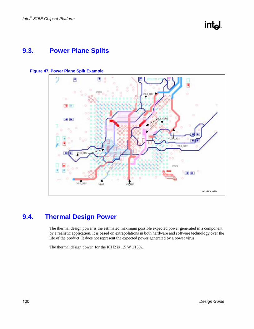
Intel® 815E Chipset Platform
R
100 Design Guide
9.3. Power Plane Splits
Figure 47. Power Plane Split Example
pwr_plane_splits
9.4. Thermal Design Power The thermal design power is the estimated maximum possible expected power generated in a component by a realistic application. It is based on extrapolations in both hardware and software technology over the life of the product. It does not represent the expected power generated by a power virus.
The thermal design power for the ICH2 is 1.5 W ±15%.
Intel® 815E Chipset Platform
R
Design Guide 101
10. I/O Subsystem
10.1. IDE Interface This section contains guidelines for connecting and routing the ICH2 IDE interface. The ICH2 has two independent IDE channels. This section provides guidelines for IDE connector cabling and motherboard design, including component and resistor placement and signal termination for both IDE channels. The ICH2 has integrated the series resistors that typically have been required on the IDE data signals (PDD[15:0] and SDD[15:0]) running to the two ATA connectors. Intel do not anticipate requiring additional series termination, but OEMs should verify the motherboard signal integrity via simulation. Additional external 0-Ω resistors can be incorporated into the design to address possible noise issues on the motherboard. The additional resistor layout increases flexibility by providing future stuffing options.
The IDE interface can be routed with 5-mil traces on 5-mil spaces and must be less than 8” long (from ICH2 to IDE connector). Additionally, the shortest IDE signal (on a given IDE channel) must be less than 0.5” shorter than the longest IDE signal (on that channel).
10.1.1. Cabling • Length of cable: Each IDE cable must be equal to or less than 18”.
• Capacitance: Less than 30 pF
• Placement: A maximum of 6” between drive connectors on the cable. If a single drive is placed on the cable it should be placed at the end of the cable. If a second drive is placed on the same cable it should be placed on the connector next closest to the end of the cable (6” away from the end of the cable).
• Grounding: Provide a direct, low-impedance chassis path between the motherboard ground and hard disk drives.
• ICH2 Placement: The ICH2 must be placed at most 8” from the ATA connector(s).
• PC99 requirement: Support Cable Select for master-slave configuration is a system design requirement of Microsoft* PC99. The CSEL signal of each ATA connector must be grounded at the host side.
10.2. Cable Detection for Ultra ATA/66 and Ultra ATA/100 The ICH2 IDE controller supports PIO, multiword (8237-style) DMA, and Ultra DMA modes 0 through 5. The ICH2 must determine the type of cable present, to configure itself for the fastest possible transfer mode that the hardware can support.
An 80-conductor IDE cable is required for Ultra ATA/66 and Ultra ATA/100. This cable uses the same 40-pin connector as the old 40-pin IDE cable. The wires in the cable alternate: ground, signal, ground, signal,…. All ground wires are tied together on the cable (and they are tied to the ground on the

Intel® 815E Chipset Platform
R
102 Design Guide
motherboard through the ground pins in the 40-pin connector). This cable conforms to the Small Form Factor Specification SFF-8049, which is obtainable from the Small Form Factor Committee.
To determine whether the ATA/66 or ATA/100 mode can be enabled, the ICH2 requires that the system software attempt to determine the type of cable used in the system. If the system software detects an 80-conductor cable, it may use any Ultra DMA mode up to the highest transfer mode supported by both the chipset and the IDE device. If a 40-conductor cable is detected, the system software must not enable modes faster than Ultra DMA Mode 2 (Ultra ATA/33).
Intel recommends that cable detection be performed using a combination host-side/device-side detection mechanism. Note that host-side detection cannot be implemented on an NLX form factor system, since this configuration does not define interconnect pins for the PDIAG#/CBLID# from the riser (containing the ATA connectors) to the motherboard. These systems must rely on the device-side detection mechanism only.
10.2.1. Combination Host-Side/Device-Side Cable Detection
Host-side detection (described in the ATA/ATAPI-4 Standard, Section 5.2.11) requires the use of two GPI pins (one for each IDE channel). The proper way to connect the PDIAG#/CBLID# signal of the IDE connector to the host is shown in the figure below. All IDE devices have a 10-kΩ pull-up resistor to 5 V on this signal. Not all GPI and GPIO pins on the ICH2 are 5-V tolerant. If non 5-V tolerant inputs are used, a resistor divider is required to prevent 5 V on the ICH2 or FWH pins. The proper value of the divider resistor is 10 kΩ (as shown in the figure below).
Figure 48. Combination Host-Side / Device-Side IDE Cable Detection
80-conductorIDE cable
IDE drive
5 V
ICH2
GPIO
GPIO
Open
IDE drive
5 V
40-conductorcable
IDE drive
5 V
PDIAG#ICH2
GPIO
GPIO
IDE drive
5 V
Resistor required fornon-5V-tolerant GPI.
PDIAG#
PDIAG#PDIAG#
Resistor required fornon-5V-tolerant GPI.
10 kΩ
10 kΩ
To secondaryIDE connector
To secondaryIDE connector
PDIAG#/CBLID#
PDIAG#/CBLID#
10 kΩ
10 kΩ
10 kΩ
10 kΩ
IDE_combo_cable_det
This mechanism allows the BIOS, after diagnostics, to sample PDIAG#/CBLID#. If the signal is High, then there is 40-conductor cable in the system and ATA modes 3, 4 and 5 must not be enabled.
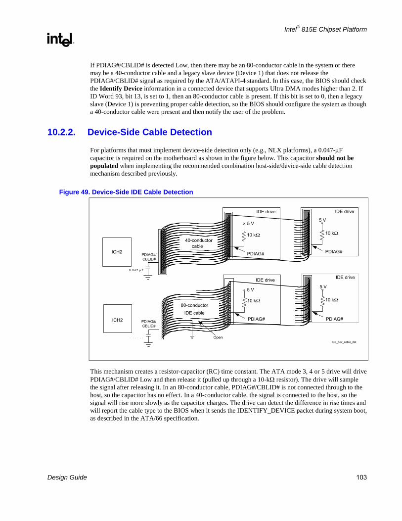
Intel® 815E Chipset Platform
R
Design Guide 103
If PDIAG#/CBLID# is detected Low, then there may be an 80-conductor cable in the system or there may be a 40-conductor cable and a legacy slave device (Device 1) that does not release the PDIAG#/CBLID# signal as required by the ATA/ATAPI-4 standard. In this case, the BIOS should check the Identify Device information in a connected device that supports Ultra DMA modes higher than 2. If ID Word 93, bit 13, is set to 1, then an 80-conductor cable is present. If this bit is set to 0, then a legacy slave (Device 1) is preventing proper cable detection, so the BIOS should configure the system as though a 40-conductor cable were present and then notify the user of the problem.
10.2.2. Device-Side Cable Detection
For platforms that must implement device-side detection only (e.g., NLX platforms), a 0.047-µF capacitor is required on the motherboard as shown in the figure below. This capacitor should not be populated when implementing the recommended combination host-side/device-side cable detection mechanism described previously.
Figure 49. Device-Side IDE Cable Detection
80-conductorIDE cable
IDE drive
5 V
ICH2
Open
IDE drive
5 V
40-conductorcable
IDE drive
5 V
PDIAG#ICH2
IDE drive
5 V
PDIAG#
PDIAG#PDIAG#PDIAG#/CBLID#
PDIAG#/CBLID#
10 kΩ
10 kΩ
10 kΩ
10 kΩ
IDE_dev_cable_det
0 .0 4 7 µ F
0 . 0 4 7 µ F
This mechanism creates a resistor-capacitor (RC) time constant. The ATA mode 3, 4 or 5 drive will drive PDIAG#/CBLID# Low and then release it (pulled up through a 10-kΩ resistor). The drive will sample the signal after releasing it. In an 80-conductor cable, PDIAG#/CBLID# is not connected through to the host, so the capacitor has no effect. In a 40-conductor cable, the signal is connected to the host, so the signal will rise more slowly as the capacitor charges. The drive can detect the difference in rise times and will report the cable type to the BIOS when it sends the IDENTIFY_DEVICE packet during system boot, as described in the ATA/66 specification.
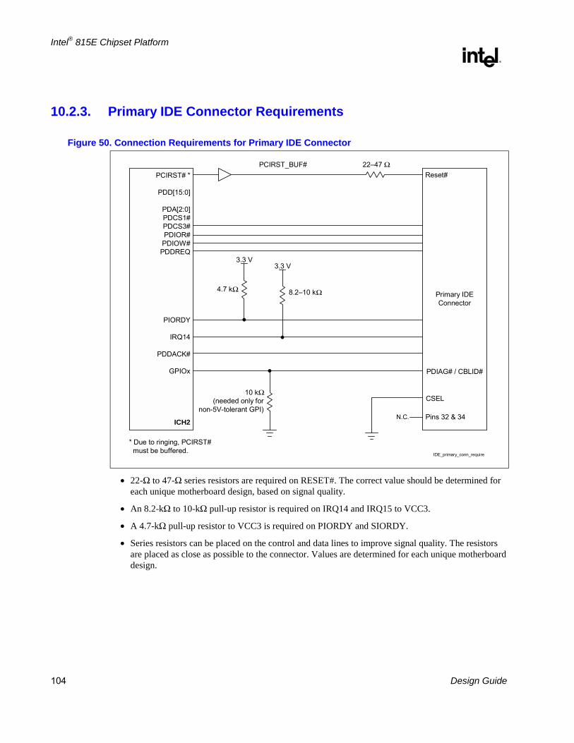
Intel® 815E Chipset Platform
R
104 Design Guide
10.2.3. Primary IDE Connector Requirements
Figure 50. Connection Requirements for Primary IDE Connector
PCIRST# *
PDD[15:0]
PDA[2:0]PDCS1#PDCS3#PDIOR#
PDIOW#PDDREQ
PIORDY
IRQ14
PDDACK#
GPIOx
ICH2
Primary IDEConnector
IDE_primary_conn_require
Reset#
PDIAG# / CBLID#
N.C. Pins 32 & 34
CSEL
* Due to ringing, PCIRST# must be buffered.
3.3 V3.3 V
4.7 kΩ 8.210 kΩ
10 kΩ(needed only for
non-5V-tolerant GPI)
2247 ΩPCIRST_BUF#
• 22-Ω to 47-Ω series resistors are required on RESET#. The correct value should be determined for each unique motherboard design, based on signal quality.
• An 8.2-kΩ to 10-kΩ pull-up resistor is required on IRQ14 and IRQ15 to VCC3.
• A 4.7-kΩ pull-up resistor to VCC3 is required on PIORDY and SIORDY.
• Series resistors can be placed on the control and data lines to improve signal quality. The resistors are placed as close as possible to the connector. Values are determined for each unique motherboard design.

Intel® 815E Chipset Platform
R
Design Guide 105
10.2.4. Secondary IDE Connector Requirements
Figure 51. Connection Requirements for Secondary IDE Connector
PCIRST# *
SDD[15:0]
SDA[2:0]SDCS1#SDCS3#SDIOR#SDIOW#SDDREQ
SIORDY
IRQ15
SDDACK#
GPIOy
ICH2
Secondary IDEConnector
IDE_secondary_conn_require
Reset#
PDIAG# / CBLID#
N.C. Pins 32 & 34
CSEL
* Due to ringing, PCIRST# must be buffered.
3.3 V3.3 V
4.7 kΩ 8.210 kΩ
10 kΩ(needed only for
non-5V-tolerant GPI)
2247 ΩPCIRST_BUF#
• 22-Ω to 47-Ω series resistors are required on RESET#. The correct value should be determined for each unique motherboard design, based on signal quality.
• An 8.2-kΩ to 10-kΩ pull-up resistor is required on IRQ14 and IRQ15 to VCC3.
• A 4.7-kΩ pull-up resistor to VCC3 is required on PIORDY and SIORDY
• Series resistors can be placed on the control and data lines to improve signal quality. The resistors are placed as close as possible to the connector. Values are determined for each unique motherboard design.

Intel® 815E Chipset Platform
R
106 Design Guide
10.3. AC’97 The ICH2 implements an AC’97 2.1-compliant digital controller. Any codec attached to the ICH2 AC-link must be AC’97 2.1 compliant, as well. Contact your codec IHV for information on 2.1-compliant products. The AC’97 2.1 specification is available on the Intel website: http://developer.intel.com/pc-supp/platform/ac97/index.htm.
The AC-link is a bidirectional, serial PCM digital stream. It handles multiple input and output data streams, as well as control register accesses, by employing a time-division-multiplexed (TDM) scheme. The AC-link architecture enables data transfer through individual frames transmitted serially. Each frame is divided into 12 outgoing and 12 incoming data streams, or slots. The architecture of the ICH2 AC-link allows a maximum of two codecs to be connected. The following figure shows a two-codec topology of the AC-link for the ICH2.
Figure 52. ICH2 AC’97– Codec Connection
AC '97 2.1controller section
of ICH2
Digital AC '972.1 controller
Primary codec
Secondary codec
AC / MC
AC / MC / AMC
ICH2_AC97_codec_conn
SDIN 0
SDIN 1
RESET#
SDOUT
SYNC
BIT_CLK
Intel has developed an advanced common connector for both AC’97 as well as networking options. This is known as the Communications and Network Riser (CNR). Refer to Section 10.4.
Clocking is provided from the primary codec on the link via BITCLK, and it is derived from a 24.576-MHz crystal or oscillator. Refer to the primary codec vendor for crystal or oscillator requirements. BITCLK is a 12.288-MHz clock driven by the primary codec to the digital controller (ICH2) and any other codec present. That clock is used as the timebase for latching and driving data.
The ICH2 supports wake-on-ring from S1-S5 via the AC’97 link. The codec asserts SDATAIN to wake the system. To provide wake capability and/or caller ID, standby power must be provided to the modem codec.
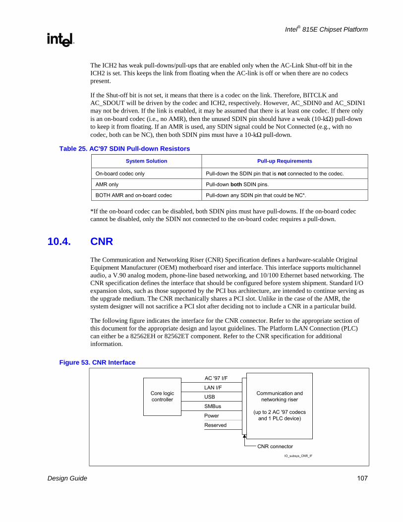
Intel® 815E Chipset Platform
R
Design Guide 107
The ICH2 has weak pull-downs/pull-ups that are enabled only when the AC-Link Shut-off bit in the ICH2 is set. This keeps the link from floating when the AC-link is off or when there are no codecs present.
If the Shut-off bit is not set, it means that there is a codec on the link. Therefore, BITCLK and AC_SDOUT will be driven by the codec and ICH2, respectively. However, AC_SDIN0 and AC_SDIN1 may not be driven. If the link is enabled, it may be assumed that there is at least one codec. If there only is an on-board codec (i.e., no AMR), then the unused SDIN pin should have a weak (10-kΩ) pull-down to keep it from floating. If an AMR is used, any SDIN signal could be Not Connected (e.g., with no codec, both can be NC), then both SDIN pins must have a 10-kΩ pull-down.
Table 25. AC'97 SDIN Pull-down Resistors
System Solution Pull-up Requirements
On-board codec only Pull-down the SDIN pin that is not connected to the codec.
AMR only Pull-down both SDIN pins.
BOTH AMR and on-board codec Pull-down any SDIN pin that could be NC*.
*If the on-board codec can be disabled, both SDIN pins must have pull-downs. If the on-board codec cannot be disabled, only the SDIN not connected to the on-board codec requires a pull-down.
10.4. CNR The Communication and Networking Riser (CNR) Specification defines a hardware-scalable Original Equipment Manufacturer (OEM) motherboard riser and interface. This interface supports multichannel audio, a V.90 analog modem, phone-line based networking, and 10/100 Ethernet based networking. The CNR specification defines the interface that should be configured before system shipment. Standard I/O expansion slots, such as those supported by the PCI bus architecture, are intended to continue serving as the upgrade medium. The CNR mechanically shares a PCI slot. Unlike in the case of the AMR, the system designer will not sacrifice a PCI slot after deciding not to include a CNR in a particular build.
The following figure indicates the interface for the CNR connector. Refer to the appropriate section of this document for the appropriate design and layout guidelines. The Platform LAN Connection (PLC) can either be a 82562EH or 82562ET component. Refer to the CNR specification for additional information.
Figure 53. CNR Interface
Communication andnetworking riser
(up to 2 AC '97 codecsand 1 PLC device)
AC '97 I/F
LAN I/F
USB
SMBus
Power
Reserved
Core logiccontroller
IO_subsys_CNR_IF
CNR connector
Intel® 815E Chipset Platform
R
108 Design Guide
10.5. USB The general guidelines for the USB interface are as follows:
• Unused USB ports should be terminated with 15-kΩ pull-down resistors on both P+/P- data lines.
• 15-Ω series resistors should be placed as close as possible to the ICH2 (<1”). These series resistors are required for source termination of the reflected signal.
• 47-pF caps must be placed as close as possible to the ICH2 and on the ICH2 side of the series resistors on the USB data lines (P0±, P1±, P2±, P3±). These caps are provided for signal quality (rise/fall time) and to help minimize EMI radiation.
• 15-kΩ ± 5% pull-down resistors should be placed on the USB side of the series resistors on the USB data lines (P0± … P3±), and they are REQUIRED for signal termination by the USB specification. The stub should be as short as possible.
• The trace impedance for the P0±…P3± signals should be 45 Ω (to ground) for each USB signal P+ or P-. When the stack-up recommended in Figure 4 is used, the USB requires 9-mil traces. The impedance is 90 Ω between the differential signal pairs P+ and P-, to match the 90-Ω USB twisted-pair cable impedance. Note that the twisted-pair’s characteristic impedance of 90 Ω is the series impedance of both wires, resulting in an individual wire presenting a 45-Ω impedance. The trace impedance can be controlled by carefully selecting the trace width, trace distance from power or ground planes, and physical proximity of nearby traces.
• USB data lines must be routed as critical signals. The P+/P- signal pair must be routed together and not parallel with other signal traces, to minimize cross-talk. Doubling the space from the P+/P- signal pair to adjacent signal traces will help to prevent cross-talk. Do not worry about cross-talk between the two P+/P- signal traces. The P+/P- signal traces must also be the same length, which will minimize the effect of common-mode current on EMI.

Intel® 815E Chipset Platform
R
Design Guide 109
The following figure illustrates the recommended USB schematic.
Figure 54. USB Data Signals
15 kΩ
15 kΩ
15 Ω
15 Ω
47 pF
47 pF
ICH
P+
P-
USB connector
< 1"
< 1"
90 Ω
45 Ω
45 Ω
Driver
Driver
USB twisted-pair cableTransmission line
Motherboard trace
Motherboard trace
usb_data_line_schem
The recommended USB trace characteristics are:
• Impedance ‘Z0’ = 45.4 Ω
• Line Delay = 160.2 ps
• Capacitance = 3.5 pF
• Inductance = 7.3 nH
• Res @ 20° C = 53.9 mΩ
10.6. ISA Implementations that require ISA support can benefit from the enhancements of the ICH2, while “ISA-less” designs are not burdened with the complexity and cost of the ISA subsystem. For information regarding the implementation of an ISA design, contact external suppliers.
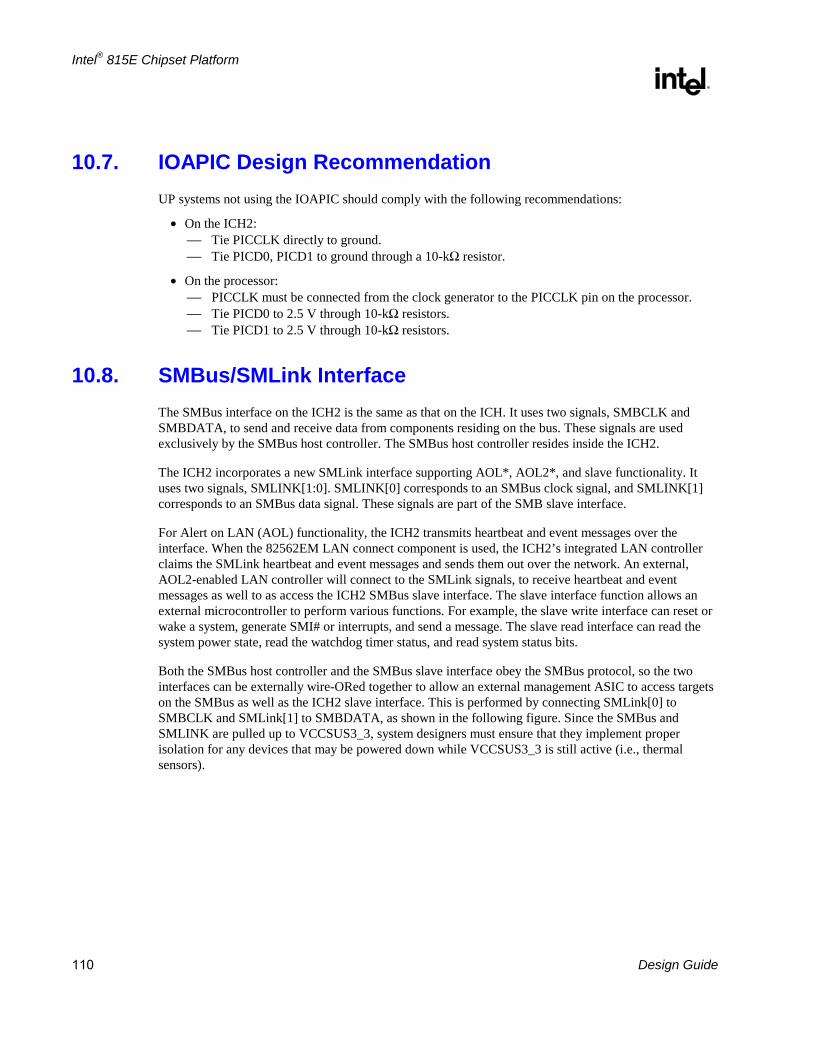
Intel® 815E Chipset Platform
R
110 Design Guide
10.7. IOAPIC Design Recommendation UP systems not using the IOAPIC should comply with the following recommendations:
• On the ICH2: Tie PICCLK directly to ground. Tie PICD0, PICD1 to ground through a 10-kΩ resistor.
• On the processor: PICCLK must be connected from the clock generator to the PICCLK pin on the processor. Tie PICD0 to 2.5 V through 10-kΩ resistors. Tie PICD1 to 2.5 V through 10-kΩ resistors.
10.8. SMBus/SMLink Interface The SMBus interface on the ICH2 is the same as that on the ICH. It uses two signals, SMBCLK and SMBDATA, to send and receive data from components residing on the bus. These signals are used exclusively by the SMBus host controller. The SMBus host controller resides inside the ICH2.
The ICH2 incorporates a new SMLink interface supporting AOL*, AOL2*, and slave functionality. It uses two signals, SMLINK[1:0]. SMLINK[0] corresponds to an SMBus clock signal, and SMLINK[1] corresponds to an SMBus data signal. These signals are part of the SMB slave interface.
For Alert on LAN (AOL) functionality, the ICH2 transmits heartbeat and event messages over the interface. When the 82562EM LAN connect component is used, the ICH2’s integrated LAN controller claims the SMLink heartbeat and event messages and sends them out over the network. An external, AOL2-enabled LAN controller will connect to the SMLink signals, to receive heartbeat and event messages as well to as access the ICH2 SMBus slave interface. The slave interface function allows an external microcontroller to perform various functions. For example, the slave write interface can reset or wake a system, generate SMI# or interrupts, and send a message. The slave read interface can read the system power state, read the watchdog timer status, and read system status bits.
Both the SMBus host controller and the SMBus slave interface obey the SMBus protocol, so the two interfaces can be externally wire-ORed together to allow an external management ASIC to access targets on the SMBus as well as the ICH2 slave interface. This is performed by connecting SMLink[0] to SMBCLK and SMLink[1] to SMBDATA, as shown in the following figure. Since the SMBus and SMLINK are pulled up to VCCSUS3_3, system designers must ensure that they implement proper isolation for any devices that may be powered down while VCCSUS3_3 is still active (i.e., thermal sensors).

Intel® 815E Chipset Platform
R
Design Guide 111
Figure 55. SMBus/SMLink Interface
82801BA
Host Controller andSlave Interface
SMBus SMBCLK
SPD Data
Temperature onThermal Sensor
NetworkInterface
Card on PCI
Microcontroller
82850
MotherboardLAN Controller
Wire OR(Optional)
SMLink0
SMLink1
SMLink
SMBDATA
smbus-link
Note: Intel does not support external access to the ICH2’s integrated LAN controller via the SMLink interface. Also, Intel does not support access to the ICH2’s SMBus slave interface by the ICH2’s SMBus host controller. The following table describes the pull-up requirements for different implementations of the SMBus and SMLink signals.
Table 26. Pull-up Requirements for SMBus and SMLink
SMBus / SMLink Use Implementation
Alert-on-LAN* signals 4.7-kΩ pull-up resistors to 3.3 VSB are required.
GPIOs Pull-up resistors to 3.3 VSB and the signals must be allowed to change states on power-up. (For example, on power-up the ICH2 will drive heartbeat messages until the BIOS programs these signals as GPIOs.) The value of the pull-up resistors depends on the loading on the GPIO signal.
Not Used 4.7-kΩ pull-up resistors to 3.3 VSB are required.
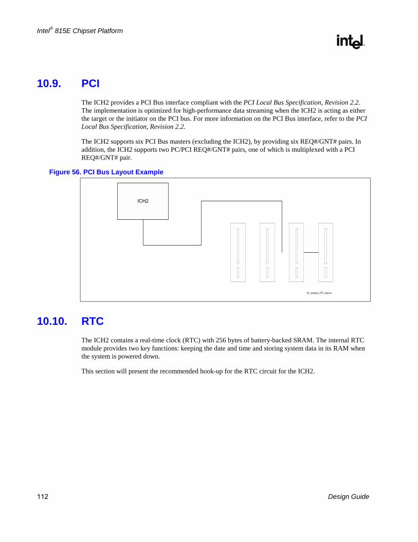
Intel® 815E Chipset Platform
R
112 Design Guide
10.9. PCI The ICH2 provides a PCI Bus interface compliant with the PCI Local Bus Specification, Revision 2.2. The implementation is optimized for high-performance data streaming when the ICH2 is acting as either the target or the initiator on the PCI bus. For more information on the PCI Bus interface, refer to the PCI Local Bus Specification, Revision 2.2.
The ICH2 supports six PCI Bus masters (excluding the ICH2), by providing six REQ#/GNT# pairs. In addition, the ICH2 supports two PC/PCI REQ#/GNT# pairs, one of which is multiplexed with a PCI REQ#/GNT# pair.
Figure 56. PCI Bus Layout Example
IO_subsys_PCI_layout
ICH2
10.10. RTC The ICH2 contains a real-time clock (RTC) with 256 bytes of battery-backed SRAM. The internal RTC module provides two key functions: keeping the date and time and storing system data in its RAM when the system is powered down.
This section will present the recommended hook-up for the RTC circuit for the ICH2.
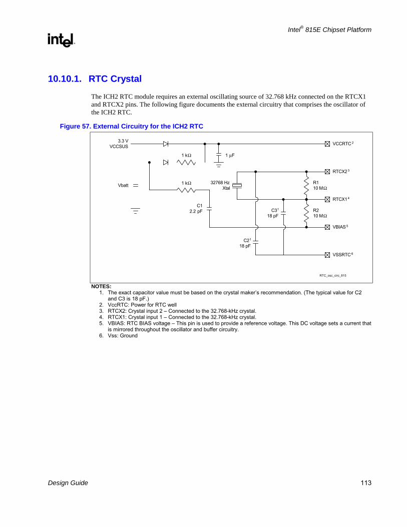
Intel® 815E Chipset Platform
R
Design Guide 113
10.10.1. RTC Crystal
The ICH2 RTC module requires an external oscillating source of 32.768 kHz connected on the RTCX1 and RTCX2 pins. The following figure documents the external circuitry that comprises the oscillator of the ICH2 RTC.
Figure 57. External Circuitry for the ICH2 RTC
C31
18 pF
3.3 VVCCSUS
1 kΩ
Vbatt 1 kΩ
C12.2 pF
32768 HzXtal
R110 MΩ
R210 MΩ
C21
18 pF
1 µF
VCCRTC 2
RTCX23
RTCX14
VBIAS 5
VSSRTC 6
RTC_osc_circ_815 NOTES:
1. The exact capacitor value must be based on the crystal makers recommendation. (The typical value for C2 and C3 is 18 pF.)
2. VccRTC: Power for RTC well 3. RTCX2: Crystal input 2 Connected to the 32.768-kHz crystal. 4. RTCX1: Crystal input 1 Connected to the 32.768-kHz crystal. 5. VBIAS: RTC BIAS voltage This pin is used to provide a reference voltage. This DC voltage sets a current that
is mirrored throughout the oscillator and buffer circuitry. 6. Vss: Ground
Intel® 815E Chipset Platform
R
114 Design Guide
10.10.2. External Capacitors
To maintain RTC accuracy, the external capacitor C1 must be 0.047 µF, and the external capacitor values (C2 and C3) should be chosen to provide the manufacturer-specified load capacitance (Cload) for the crystal, when combined with the parasitic capacitance of the trace, socket (if used), and package. When the external capacitor values are combined with the capacitance of the trace, socket, and package, the closer the capacitor value can be matched to the actual load capacitance of the crystal used, the more accurate the RTC will be.
The following equation can be used to choose the external capacitance values (C2 and C3):
Cload = (C2 * C3) / (C2 + C3) + Cparasitic
C3 can be chosen such that C3 > C2. Then C2 can be trimmed to obtain 32.768 kHz.
10.10.3. RTC Layout Considerations • Keep the RTC lead lengths as short as possible. Approximately 0.25” is sufficient.
• Minimize the capacitance between Xin and Xout in the routing.
• Put a ground plane under the XTAL components.
• Don’t route switching signals under the external components (unless on the other side of the board).
• The oscillator VCC should be clean. Use a filter, such as an RC low-pass or a ferrite inductor.
10.10.4. RTC External Battery Connection
The RTC requires an external battery connection to maintain its functionality and its RAM while the ICH2 is not powered by the system.
Example batteries include the Duracell* 2032, 2025 or 2016 (or equivalent), which give many years of operation. Batteries are rated by storage capacity. The battery life can be calculated by dividing the capacity by the average current required. For example, if the battery storage capacity is 170 mAh (assumed usable) and the average current required is 3 µA, the battery life will be at least:
170,000 µAh / 3 µA = 56,666 h = 6.4 years
The voltage of the battery can affect the RTC accuracy. In general, when the battery voltage decays, the RTC accuracy also decreases. High accuracy can be obtained when the RTC voltage is within the range 3.0 V to 3.3 V.
The battery must be connected to the ICH2 via an isolation Schottky diode circuit. The Schottky diode circuit allows the ICH2 RTC well to be powered by the battery when system power is unavailable, but by system power when it is available. So, the diodes are set to be reverse-biased when system power is unavailable. The following figures shows an example of the used diode circuitry.
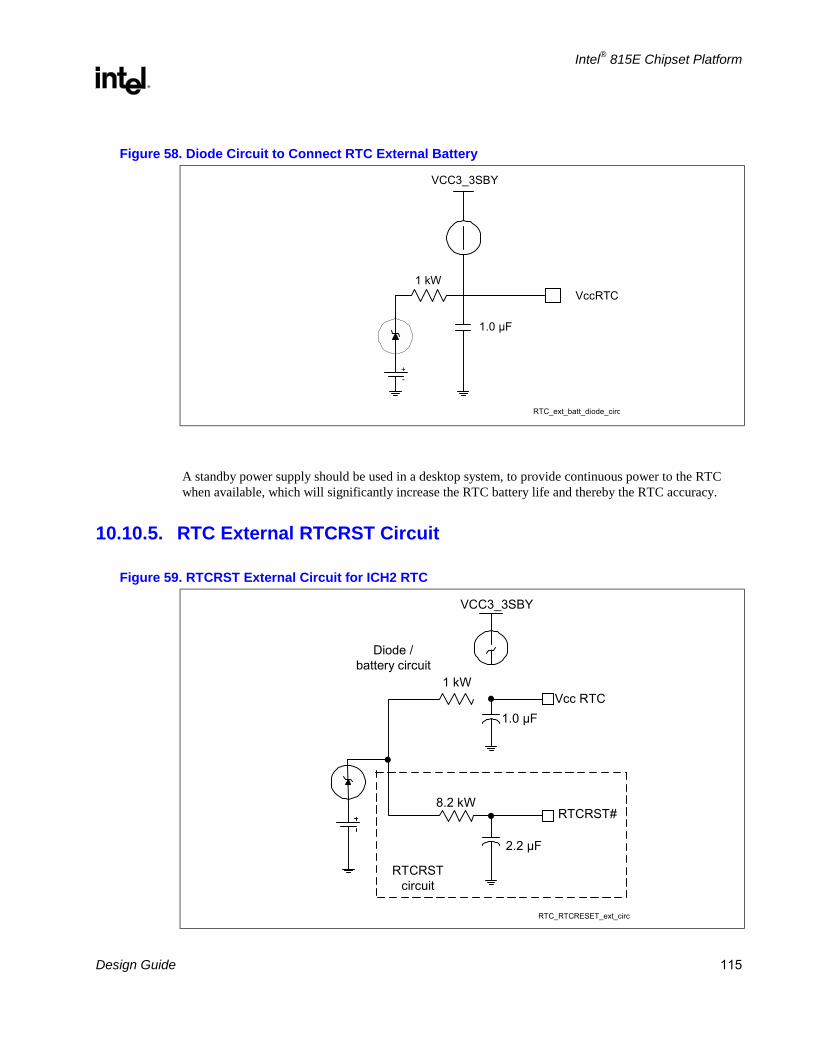
Intel® 815E Chipset Platform
R
Design Guide 115
Figure 58. Diode Circuit to Connect RTC External Battery
VCC3_3SBY
VccRTC
1.0 µF
1 kW
RTC_ext_batt_diode_circ
-+
A standby power supply should be used in a desktop system, to provide continuous power to the RTC when available, which will significantly increase the RTC battery life and thereby the RTC accuracy.
10.10.5. RTC External RTCRST Circuit
Figure 59. RTCRST External Circuit for ICH2 RTC
VCC3_3SBY
Vcc RTC1.0 µF
1 kW
2.2 µF
8.2 kWRTCRST#
RTCRSTcircuit
Diode /battery circuit
RTC_RTCRESET_ext_circ

Intel® 815E Chipset Platform
R
116 Design Guide
The ICH2 RTC requires some additional external circuitry. The RTCRST# signal is used to reset the RTC well. The external capacitor and the external resistor between RTCRST# and the RTC battery (Vbat) were selected to create an RC time delay, such that RTCRST# will go High some time after the battery voltage is valid. The RC time delay should be within the range of 10–20 ms. When RTCRST# is asserted, bit 2 (RTC_PWR_STS) in the GEN_PMCON_3 (General PM Configuration 3) register is set to 1 and remains set until cleared by software. As a result, when the system boots, the BIOS knows that the RTC battery has been removed.
This RTCRST# circuit is combined with the diode circuit (see previous figure), which allows the RTC well to be powered by the battery when system power is unavailable. The previous figure shows an example of this circuitry when used in conjunction with the external diode circuit.
10.10.6. RTC Routing Guidelines • All RTC OSC signals (RTCX1, RTCX2, VBIAS) should all be routed with trace lengths less than
1”. The shorter, the better.
• Minimize the capacitance between RTCX1 and RTCX2 in the routing. (Optimally, there would be a ground line between them.)
• Put a ground plane under all external RTC circuitry.
• Don’t route any switching signals under the external components (unless on the other side of the ground plane).
10.10.7. VBIAS DC Voltage and Noise Measurements • All RTC OSC signals (RTCX1, RTCX2, VBIAS) should all be routed with trace lengths less than
1”. The shorter, the better.
• Steady-state VBIAS is a DC voltage of about 0.38 V ± .06 V.
• When the battery is inserted, VBIAS will be “kicked” to about 0.7–1.0 V, but it will return to its DC value within a few ms.
• Noise on VBIAS must be kept to a minimum (200 mV or less).
• VBIAS is very sensitive and cannot be directly probed, but it can be probed through a .01-µF capacitor.
• Excessive noise on VBIAS can cause the ICH2 internal oscillator to misbehave or even stop completely.
• To minimize VBIAS noise, it is necessary to implement the routing guidelines described previously as well as the required external RTC circuitry, as described in the Intel® 82801BA I/O Controller Hub 2 (ICH2) Datasheet.
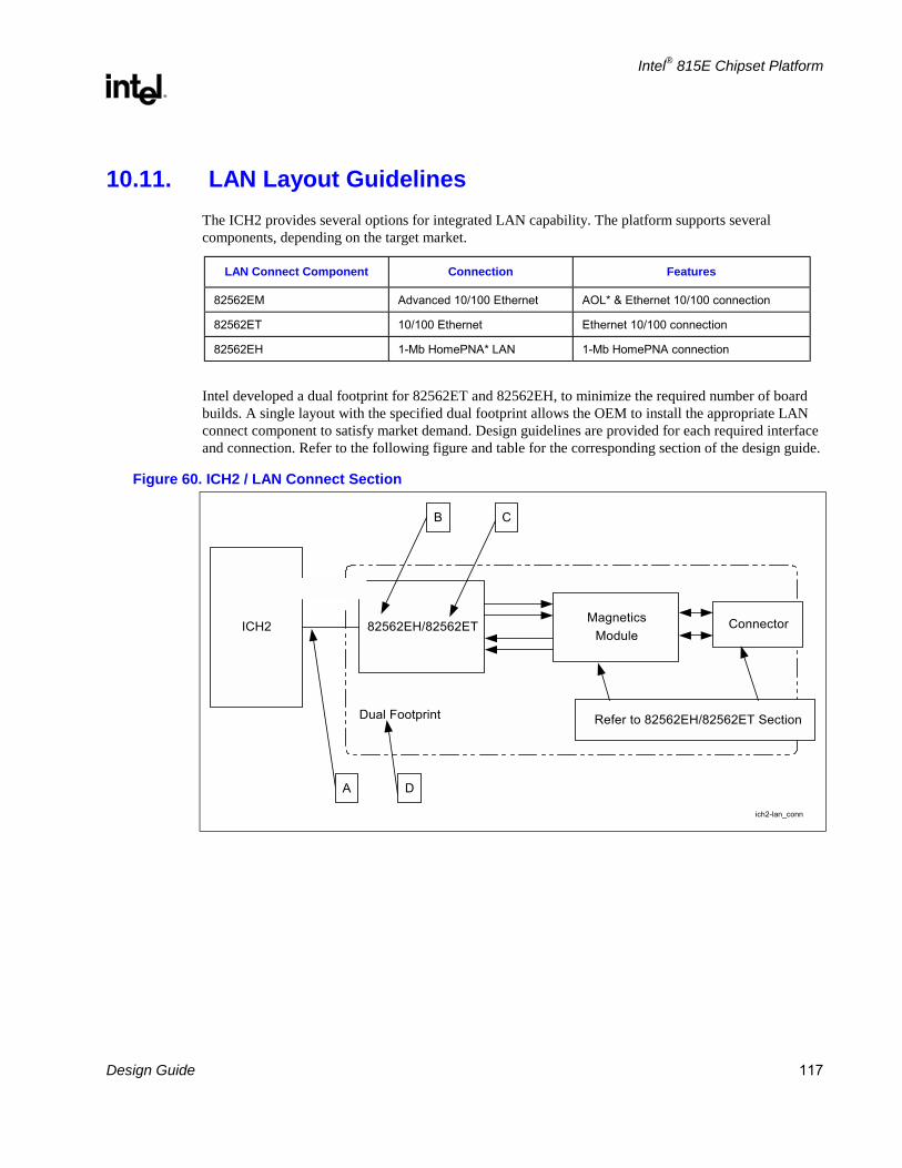
Intel® 815E Chipset Platform
R
Design Guide 117
10.11. LAN Layout Guidelines The ICH2 provides several options for integrated LAN capability. The platform supports several components, depending on the target market.
LAN Connect Component Connection Features
82562EM Advanced 10/100 Ethernet AOL* & Ethernet 10/100 connection
82562ET 10/100 Ethernet Ethernet 10/100 connection
82562EH 1-Mb HomePNA* LAN 1-Mb HomePNA connection
Intel developed a dual footprint for 82562ET and 82562EH, to minimize the required number of board builds. A single layout with the specified dual footprint allows the OEM to install the appropriate LAN connect component to satisfy market demand. Design guidelines are provided for each required interface and connection. Refer to the following figure and table for the corresponding section of the design guide.
Figure 60. ICH2 / LAN Connect Section
ich2-lan_conn
Dual Footprint
82562EH/82562ETICH2Magnetics
ModuleConnector
A
B
D
C
Refer to 82562EH/82562ET Section
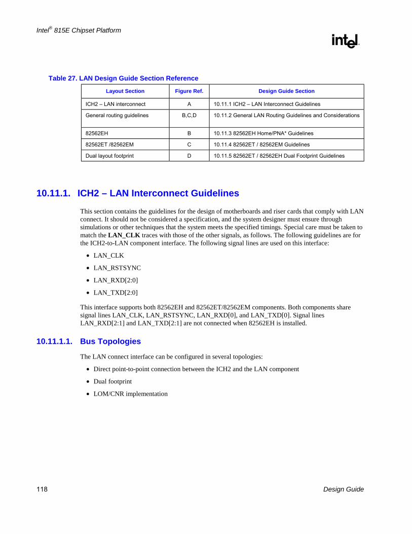
Intel® 815E Chipset Platform
R
118 Design Guide
Table 27. LAN Design Guide Section Reference
Layout Section Figure Ref. Design Guide Section
ICH2 LAN interconnect A 10.11.1 ICH2 LAN Interconnect Guidelines
General routing guidelines B,C,D 10.11.2 General LAN Routing Guidelines and Considerations
82562EH B 10.11.3 82562EH Home/PNA* Guidelines
82562ET /82562EM C 10.11.4 82562ET / 82562EM Guidelines
Dual layout footprint D 10.11.5 82562ET / 82562EH Dual Footprint Guidelines
10.11.1. ICH2 – LAN Interconnect Guidelines
This section contains the guidelines for the design of motherboards and riser cards that comply with LAN connect. It should not be considered a specification, and the system designer must ensure through simulations or other techniques that the system meets the specified timings. Special care must be taken to match the LAN_CLK traces with those of the other signals, as follows. The following guidelines are for the ICH2-to-LAN component interface. The following signal lines are used on this interface:
• LAN_CLK
• LAN_RSTSYNC
• LAN_RXD[2:0]
• LAN_TXD[2:0]
This interface supports both 82562EH and 82562ET/82562EM components. Both components share signal lines LAN_CLK, LAN_RSTSYNC, LAN_RXD[0], and LAN_TXD[0]. Signal lines LAN_RXD[2:1] and LAN_TXD[2:1] are not connected when 82562EH is installed.
10.11.1.1. Bus Topologies
The LAN connect interface can be configured in several topologies:
• Direct point-to-point connection between the ICH2 and the LAN component
• Dual footprint
• LOM/CNR implementation
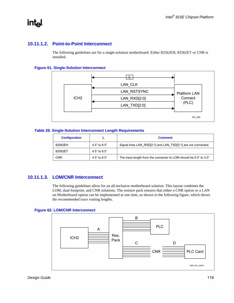
Intel® 815E Chipset Platform
R
Design Guide 119
10.11.1.2. Point-to-Point Interconnect
The following guidelines are for a single-solution motherboard. Either 82562EH, 82562ET or CNR is installed.
Figure 61. Single-Solution Interconnect
lan_p2p
ICH2Platform LAN
Connect(PLC)
LAN_TXD[2:0]
LAN_RXD[2:0]
LAN_RSTSYNC
LAN_CLK
L
Table 28. Single-Solution Interconnect Length Requirements
Configuration L Comment
82562EH 4.5 to 8.5 Signal lines LAN_RXD[2:1] and LAN_TXD[2:1] are not connected.
82562ET 4.5 to 8.5
CNR 4.5 to 8.5 The trace length from the connector to LOM should be 0.5 to 3.0
10.11.1.3. LOM/CNR Interconnect
The following guidelines allow for an all-inclusive motherboard solution. This layout combines the LOM, dual-footprint, and CNR solutions. The resistor pack ensures that either a CNR option or a LAN on Motherboard option can be implemented at one time, as shown in the following figure, which shows the recommended trace routing lengths.
Figure 62. LOM/CNR Interconnect
lom-cnr_conn
ICH2 Res.Pack
CNR PLC Card
B
A PLC
C D

Intel® 815E Chipset Platform
R
120 Design Guide
Table 29. LOM/CNR Length Requirements
Configuration A B C D
82562EH 0.5 to 6.0 4.0 to (10.0 A)
82562ET 0.5 to 7.0 3.0 to (10.0 A)
Dual footprint 0.5 to 6.0 4.0 to (10.0 A)
82562ET/EH card* 0.5 to 6.5 2.5 to (9 A) 0.5 to 3.0 NOTES:
1. The total trace length should not exceed 13.
Additional guidelines for this configuration are as follows:
• Stubs due to the resistor pack should not be present on the interface.
• The resistor pack value can be 0 Ω or 22 Ω.
• LAN on Motherboard PLC can be a dual-footprint configuration.
10.11.1.4. Signal Routing and Layout
LAN connect signals must be carefully routed on the motherboard to meet the timing and signal quality requirements of this interface specification. The following are some of the general guidelines that should be followed. It is recommended that the board designer simulate the board routing, to verify that the specifications are met for flight times and skews due to trace mismatch and cross-talk. On the motherboard, the length of each data trace is either equal in length to the LAN_CLK trace or up to 0.5” shorter than the LAN_CLK trace. (LAN_CLK should always be the longest motherboard trace in each group.)
Figure 63. LAN_CLK Routing Example
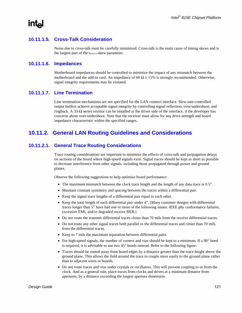
Intel® 815E Chipset Platform
R
Design Guide 121
10.11.1.5. Cross-Talk Consideration
Noise due to cross-talk must be carefully minimized. Cross-talk is the main cause of timing skews and is the largest part of the tRMATCH skew parameter.
10.11.1.6. Impedances
Motherboard impedances should be controlled to minimize the impact of any mismatch between the motherboard and the add-in card. An impedance of 60 Ω ± 15% is strongly recommended. Otherwise, signal integrity requirements may be violated.
10.11.1.7. Line Termination
Line termination mechanisms are not specified for the LAN connect interface. Slew-rate-controlled output buffers achieve acceptable signal integrity by controlling signal reflection, over/undershoot, and ringback. A 33-Ω series resistor can be installed at the driver side of the interface, if the developer has concerns about over/undershoot. Note that the receiver must allow for any drive strength and board impedance characteristic within the specified ranges.
10.11.2. General LAN Routing Guidelines and Considerations
10.11.2.1. General Trace Routing Considerations
Trace routing considerations are important to minimize the effects of cross-talk and propagation delays on sections of the board where high-speed signals exist. Signal traces should be kept as short as possible to decrease interference from other signals, including those propagated through power and ground planes.
Observe the following suggestions to help optimize board performance:
• The maximum mismatch between the clock trace length and the length of any data trace is 0.5”. • Maintain constant symmetry and spacing between the traces within a differential pair. • Keep the signal trace lengths of a differential pair equal to each other. • Keep the total length of each differential pair under 4”. (Many customer designs with differential
traces longer than 5” have had one or more of the following issues: IEEE phy conformance failures, excessive EMI, and/or degraded receive BER.)
• Do not route the transmit differential traces closer than 70 mils from the receive differential traces. • Do not route any other signal traces both parallel to the differential traces and closer than 70 mils
from the differential traces. • Keep to 7 mils the maximum separation between differential pairs. • For high-speed signals, the number of corners and vias should be kept to a minimum. If a 90° bend
is required, it is advisable to use two 45° bends instead. Refer to the following figure. • Traces should be routed away from board edges by a distance greater than the trace height above the
ground plane. This allows the field around the trace to couple more easily to the ground plane rather than to adjacent wires or boards.
• Do not route traces and vias under crystals or oscillators. This will prevent coupling to or from the clock. And as a general rule, place traces from clocks and drives at a minimum distance from apertures, by a distance exceeding the largest aperture dimension.

Intel® 815E Chipset Platform
R
122 Design Guide
Figure 64. Trace Routing
45
10.11.2.1.1. Trace Geometry and Length
The key factors in controlling trace EMI radiation are the trace length and the ratio of trace width to trace height above the ground plane. To minimize trace inductance, high-speed signals and signal layers close to a ground or power plane should be as short and wide as practical. Ideally, this ratio of trace width to height above the ground plane is between 1:1 and 3:1. To maintain trace impedance, the width of the trace should be modified when changing from one board layer to another, if the two layers are not equidistant from the power or ground plane. Differential trace impedances should be controlled to ~100 Ω. It is necessary to compensate for trace-to-trace edge coupling, which can lower the differential impedance by 10 Ω, when the traces within a pair are closer than 0.030” (edge to edge).
Traces between decoupling and I/O filter capacitors should be as short and wide as practical. Long-and-thin traces are more inductive and would reduce the intended effect of the decoupling capacitors. For similar reasons, traces to I/O signals and signal terminations should be as short as possible. Vias to the decoupling capacitors should have diameters sufficiently large to decrease series inductance.
10.11.2.1.2. Signal Isolation
Comply with the following rules for signal isolation:
• Separate and group signals by function on separate layers, if possible. Maintain a gap of 70 mils between all differential pairs (Phoneline and Ethernet) and other nets, but group together associated differential pairs.
Note: Over the length of the trace run, each differential pair should be at least 0.3” away from any parallel signal trace.
• Physically group together all components associated with one clock trace, to reduce trace length and radiation.
• Isolate I/O signals from high-speed signals to minimize cross-talk, which can increase EMI emission and susceptibility to EMI from other signals.
• Avoid routing high-speed LAN or Phoneline traces near other high-frequency signals associated with a video controller, cache controller, processor or other similar device.
Intel® 815E Chipset Platform
R
Design Guide 123
10.11.2.2. Power and Ground Connections
Comply with the following rules and guidelines for power and ground connections:
• All VCC pins should be connected to the same power supply.
• All VSS pins should be connected to the same ground plane.
• Use one decoupling capacitor per power pin for optimized performance.
• Place decoupling as close as possible to power pins.
10.11.2.2.1. General Power and Ground Plane Considerations
To properly implement the common-mode choke functionality of the magnetics module, the chassis or output ground (secondary side of transformer) should be physically separated from the digital or input ground (primary side) by at least 100 mils.
Figure 65. Ground Plane Separation
GND_Plane_Separ
Separate Chassis Ground Plane
0.01" minimum separation
Magnetics Module
Separate Chassis Ground Plane Ground plane
Good grounding requires minimizing inductance levels in the interconnections. Keeping ground returns short, signal loop areas small, and power inputs bypassed to signal return will significantly reduce EMI radiation.

Intel® 815E Chipset Platform
R
124 Design Guide
Comply with the following rules to help reduce circuit inductance in both backplanes and motherboards:
• Route traces over a continuous plane with no interruptions (i.e., do not route over a split plane). If there are vacant areas on a ground or power plane, avoid routing signals over the vacant area. This will increase inductance and EMI radiation levels.
• To reduce coupling, separate noisy digital grounds from analog grounds.
• Noisy digital grounds may affect sensitive DC subsystems.
• All ground vias should be connected to every ground plane, and every power via should be connected to all power planes at equal potential. This helps reduce circuit inductance.
• Physically locate grounds between a signal path and its return. This will minimize the loop area.
• Avoid fast rise/fall times as much as possible. Signals with fast rise and fall times contain many high-frequency harmonics, which can radiate EMI.
• The ground plane beneath the filter/transformer module should be split. The RJ45 and/or RJ11 connector side of the transformer module should have chassis ground beneath it. Splitting the ground planes beneath the transformer minimizes noise coupling between the primary and secondary sides of the transformer and between adjacent coils in the transformer. There should not be a power plane under the magnetics module.
• Create a spark gap between pins 2 through 5 of the Phoneline connector(s) and a shield ground of 1.5 mm (59.0 mil). This critical requirement is needed to pass FCC Part 68 testing of the Phoneline connection.
10.11.2.3. A 4-Layer Board Design
Top-Layer Routing
Sensitive analog signals are routed completely on the top layer without the use of vias. This allows tight control of signal integrity and removes any impedance inconsistencies due to layer changes.
Ground Plane
It is advisable to provide a layout split (100 mils) of the ground plane under the magnetics module between the primary and secondary side of the module.
Power Plane
Physically separate digital and analog power planes must be provided to prevent digital switching noise from being coupled into the analog power supply planes VDD_A. Analog power may be a metal fill “island,” separated from digital power, and better filtered than digital power.
Bottom-Layer Routing
Digital high-speed signals, which include all LAN interconnect interface signals, are routed on the bottom layer.

Intel® 815E Chipset Platform
R
Design Guide 125
10.11.2.4. Common Physical Layout Issues
Common physical layer design and layout mistakes in LAN On Motherboard designs are as follows: 1. Unequal length of the two traces within a differential pair. Inequalities create common-mode noise
and distort the transmit or receive waveforms. 2. Lack of symmetry between the two traces within a differential pair. (For each component and/or
via that one trace encounters, the other trace must encounter the same component or a via at the same distance from the PLC.) Asymmetry can create common-mode noise, and distort the waveforms.
3. Excessive distance between the PLC and the magnetics or between the magnetics and the RJ-45/11 connector. When the total distance exceeds approximately 4”, it can become extremely difficult to design a spec-compliant LAN product. If they are long, traces on FR4 (fiberglass-epoxy substrate) will attenuate the analog signals. Also, any impedance mismatch in the traces will be increased if they are longer (see item 9).
4. Routing any other trace parallel to and close to one of the differential traces. Cross-talk on the receive channel will induce degraded long-cable BER. When cross-talk gets onto the transmit channel, it can cause excessive emissions (below the FCC standard) and can cause poor transmit BER on long cables. Other signals should be kept at least 0.3” from the differential traces.
5. Routing the transmit differential traces next to the receive differential traces. The transmit trace closest to one of the receive traces will put more cross-talk onto the closest receive trace, which can greatly degrade the receiver's BER over long cables. After exiting the PLC, the transmit traces should be kept 0.3” or more away from the nearest receive trace. In the vicinities where the traces enter or exit the magnetics, the RJ-45/11 and the PLC are the only possible exceptions.
6. Use of an inferior magnetics module. The magnetics modules used by Intel have been fully tested for IEEE PLC conformance, long-cable BER problems, and emissions and immunity. (Inferior magnetics modules often have less common-mode rejection and/or no auto-transformer in the transmit channel.)
7. Another common mistake is using an 82555 or 82558 physical layer schematic in a PLC design. The transmit terminations and decoupling are different, and there also are differences in the receive circuit. Use the appropriate reference schematic or application notes.
8. Not using (or incorrectly using) the termination circuits for the unused pins at the RJ-45/11 and for the wire-side center-taps of the magnetics modules. These unused RJ pins and wire-side center-taps must be correctly referenced to chassis ground via the proper value resistor and capacitor or termination plane. If these are not terminated properly, there can be emission (FCC) problems, IEEE conformance issues, and long-cable noise (BER) problems. The application notes contain schematics that illustrate the proper termination for these unused RJ pins and the magnetics center-taps.
9. Incorrect differential trace impedances. It is important to have ~100 Ω impedance between the two traces within a differential pair. This becomes even more important as the differential traces become longer. It is very common to see customer designs that have differential trace impedances between 75 Ω and 85 Ω, even when the designers think they have designed for 100 Ω. (To calculate the differential impedance, many impedance calculators only multiply the single-ended impedance by two. This does not take into account edge-to-edge capacitive coupling between the two traces. When the two traces within a differential pair are kept close (see Note) to each other, the edge coupling can lower the effective differential impedance by 5 Ω to 20 Ω. A 10-Ω to 15-Ω drop in impedance is common.) Short traces will have fewer problems if the differential impedance is a little off.
Intel® 815E Chipset Platform
R
126 Design Guide
10. Another common problem is to use a too-large capacitor between the transmit traces and/or too much capacitance from the magnetic's transmit center-tap (on the 82562ET side of the magnetics) to ground. Using capacitors with capacitances exceeding a few pF in either of these locations can slow the 100-Mbps rise and fall times so much that they fail the IEEE rise time and fall time specs, which will cause the return loss to fail at higher frequencies and will degrade the transmit BER performance. Caution should be exercised if a cap is put in either of these locations. If a cap is used, it should almost certainly be less than 22 pF. (Reasonably good success has been achieved by using 6-pF to 12-pF values in past designs.) Unless there is some overshoot in the 100-Mbps mode, these caps are not necessary.
Note: It is important to keep the two traces within a differential pair close to each other. Keeping them close improves their immunity to cross-talk and other sources of common-mode noise. Keeping them close results in lower emissions (i.e., FCC compliance) from the transmit traces as well as a better receive BER for the receive traces. Close should be considered to be less than 0.030” between the two traces within a differential pair. 0.008” to 0.012” trace-to-trace spacing is recommended.
10.11.3. 82562EH Home/PNA* Guidelines
Related Documents
Title Location
82562EH HomePNA 1-Mb/s Physical Layer Interface Datasheet (Order number: 278313)
Intels website for developers is at: http://developer.intel.com
82562EH HomePNA 1-Mb/s Physical Layer Interface Brief Datasheet (Order number: 278314)
Intels website for developers is at: http://developer.intel.com
For correct LAN performance, designers must follow the general guidelines outlined in Section 10.11.2. Additional guidelines for implementing a 82562EH Home/PNA* LAN connect component are as follows.
10.11.3.1. Power and Ground Connections
Obey the following rule for power and ground connections:
• For best performance, place decoupling capacitors on the back side of the PCB, directly under the 82562EH, with equal distance from both pins of the capacitor to power/ground.
The analog power supply pins for 82562EH (VCCA, VSSA) should be isolated from the digital VCC and VSS through the use of ferrite beads. In addition, adequate filtering and decoupling capacitors should be provided between VCC and VSS as well as the VCCA and VSSA power supplies.
Intel® 815E Chipset Platform
R
Design Guide 127
10.11.3.2. Guidelines for 82562EH Component Placement
Component placement can affect the signal quality, emissions, and temperature of a board design. This section discusses guidelines for component placement.
Careful component placement can:
• Decrease potential problems directly related to electromagnetic interference (EMI), which could result in failure to meet FCC specifications.
• Simplify the task of routing traces. To some extent, component orientation will affect the complexity of trace routing. The overall objective is to minimize turns and crossovers between traces.
It is important to minimize the space needed for the HomePNA LAN interface, because all other interfaces will compete for physical space on a motherboard near the connector edge. As with most subsystems, the HomePNA LAN circuits must be as close as possible to the connector. Thus, it is imperative that all designs be optimized to fit in a very small space.
10.11.3.3. Crystals and Oscillators
To minimize the effects of EMI, clock sources should not be placed near I/O ports or board edges. Radiation from these devices may be coupled onto the I/O ports or out of the system chassis. Crystals should also be kept away from the HomePNA magnetics module to prevent communication interference. If they exist, the crystal’s retaining straps should be grounded to prevent the possibility of radiation from the crystal case, and the crystal should lie flat against the PC board to provide better coupling of the electromagnetic fields to the board.
For noise-free and stable operation, place the crystal and associated discrete components as close as possible to the 82562EH. Minimize the length and do not route any noisy signals in this area.
10.11.3.4. Phoneline HPNA Termination
The transmit/receive differential signal pair is terminated with a pair of 51.1-Ω (1%) resistors. This parallel termination should be placed close to the 82562EH. The center, common point between the 51.1-Ω resistors is connected to a voltage-divider network. The termination is shown in the following figure.

Intel® 815E Chipset Platform
R
128 Design Guide
Figure 66. 82562EH Termination
123456
T a b
T a b
123456
T a b
T a b
8Phone / modem
Shield ground
Line 8
7
7
IO_subsys_82562EH_term
1500 pF 1500 pF
6.8 µH 6.8 µH
6.8 µH 6.8 µH
0
T10
9
1
23
B6008
rx_tx_pn
rx_tx_n
0.022 µF
51.1 Ω
51.1 Ω
806 Ω
806 Ω
A+3.3 V
Tip
Ring
The filter and magnetics component T1 integrates the required filter network, high-voltage impulse protection, and transformer to support the HomePNA LAN interface.
One RJ-11 jack (labeled “LINE” in the previous figure) allows the node to be connected to the Phoneline, and the second jack (labeled “PHONE” in the previous figure) allows other down-line devices to be connected at the same time. This second connector is not required by the HomePNA. However, typical PCI adapters and PC motherboard implementations are likely to include it for user convenience.
A low-pass filter, setup in-line with the second RJ-11 jack, also is recommended by the HomePNA to minimize interference between the HomeRun connection and a POTs voice or modem connection on the second jack. This restricts of the type of devices connected to the second jack as the pass-band of this filter is set approximately at 1.1 MHz. Refer to the HomePNA website (www.homepna.org) for up-to-date information and recommendations regarding the use of this low-pass filter to meet HomePNA certifications.

Intel® 815E Chipset Platform
R
Design Guide 129
10.11.3.5. Critical Dimensions
There are three dimensions to consider during layout. Distance ‘B’ from the line RJ11 connector to the magnetics module, distance ‘C’ from the phone RJ11 to the LPF (if implemented), and distance ‘A’ from 82562EH to the magnetics module (see the following figure).
Figure 67. Critical Dimensions for Component Placement
Critical_place
ICH2 82562ET MagneticsModule
LineRJ11
BA
EEPROM
LPF PhoneRJ11
C
Distance Priority Guideline
B 1 < 1
A 2 < 1
C 3 < 1
10.11.3.5.1. Distance from Magnetics Module to Line RJ11
This distance ‘B’ should be given highest priority and should be less then 1”. Regarding trace symmetry, route differential pairs with consistent separation and with exactly the same lengths and physical dimensions.
Asymmetrical and unequally long differential pairs contribute to common-mode noise. This can degrade the receive circuit performance and contribute to emissions radiated from the transmit side.

Intel® 815E Chipset Platform
R
130 Design Guide
10.11.3.5.2. Distance from 82562EH to Magnetics Module
Due to the high speed of signals present, distance ‘A’ between the 82562EH and the magnetics should also be less than 1”, but should be second priority relative to distance from connects to the magnetics module.
Generally speaking, any section of trace intended for use with high-speed signals should be subject to proper termination practices. Proper signal termination can reduce reflections caused by impedance mismatches between the device and traces route. The reflections of a signal may have a high-frequency component that may contribute more EMI than the original signal itself.
10.11.3.5.3. Distance from LPF to Phone RJ11
This distance ‘C’ should be less then 1”. Regarding trace symmetry, route differential pairs with consistent separation and with exactly the same lengths and physical dimensions.
Asymmetrical and unequally long differential pairs contribute to common-mode noise. This can degrade the receive circuit performance and contribute to emissions radiated from the transmit side
10.11.4. 82562ET / 82562EM Guidelines
Related Documents • 82562ET Platform LAN Connect (PLC) Datasheet
• PCB Design for the 82562 ET/EM Platform LAN Connect
For correct LAN performance, designers must follow the general guidelines outlined in Section 10.11.2. Additional guidelines for implementing a 82562ET or 82562EM LAN connect component are as follows.
10.11.4.1. Guidelines for 82562ET / 82562EM Component Placement
Component placement can affect the signal quality, emissions, and temperature of a board design. This section provides guidelines for component placement.
Careful component placement can:
• Decrease potential problems directly related to electromagnetic interference (EMI), which could result in failure to meet FCC and IEEE test specifications.
• Simplify the task of routing traces. To some extent, component orientation will affect the complexity of trace routing. The overall objective is to minimize turns and crossovers between traces.
It is important to minimize the space needed for the Ethernet LAN interface, because all other interfaces will compete for physical space on a motherboard near the connector edge. As with most subsystems, the Ethernet LAN circuits must be as close as possible to the connector. Thus, it is imperative that all designs be optimized to fit in a very small space.
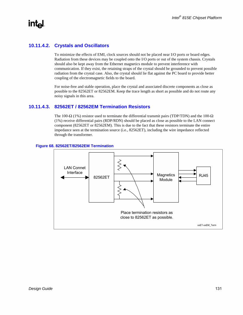
Intel® 815E Chipset Platform
R
Design Guide 131
10.11.4.2. Crystals and Oscillators
To minimize the effects of EMI, clock sources should not be placed near I/O ports or board edges. Radiation from these devices may be coupled onto the I/O ports or out of the system chassis. Crystals should also be kept away from the Ethernet magnetics module to prevent interference with communication. If they exist, the retaining straps of the crystal should be grounded to prevent possible radiation from the crystal case. Also, the crystal should lie flat against the PC board to provide better coupling of the electromagnetic fields to the board.
For noise-free and stable operation, place the crystal and associated discrete components as close as possible to the 82562ET or 82562EM. Keep the trace length as short as possible and do not route any noisy signals in this area.
10.11.4.3. 82562ET / 82562EM Termination Resistors
The 100-Ω (1%) resistor used to terminate the differential transmit pairs (TDP/TDN) and the 100-Ω (1%) receive differential pairs (RDP/RDN) should be placed as close as possible to the LAN connect component (82562ET or 82562EM). This is due to the fact that these resistors terminate the entire impedance seen at the termination source (i.e., 82562ET), including the wire impedance reflected through the transformer.
Figure 68. 82562ET/82562EM Termination
xxET-xxEM_Term
82562ET MagneticsModule
RJ45
Place termination resistors asclose to 82562ET as possible.
LAN ConnetInterface

Intel® 815E Chipset Platform
R
132 Design Guide
10.11.4.4. Critical Dimensions
Figure 69. Critical Dimensions for Component Placement
There are two dimensions to consider during layout. Distance ‘B’ from the line RJ45 connector to the magnetics module and distance ‘A’ from the 82562ET or 82562EM to the magnetics module (see the following figure).
Critical_place_2
ICH2 82562EH MagneticsModule
LineRJ11
BA
EEPROM
LPF PhoneRJ11
C
Distance Priority Guideline
A 1 < 1
B 2 < 1
Distance from Magnetics Module to RJ45
The distance A in the previous figure should be given the highest priority in board layout. The separation between the magnetics module and the RJ45 connector should be kept less than 1”. The following trace characteristics are important and should be observed:
• Differential impedance: The differential impedance should be 100 Ω. The single-ended trace impedance will be approximately 50 Ω. However, the differential impedance can also be affected by the spacing between the traces.
• Trace Symmetry: Differential pairs (e.g., TDP and TDN) should be routed with consistent separation and with exactly the same lengths and physical dimensions (e.g., width).
Caution: Asymmetric and unequal length traces in the differential pairs contribute to common-mode noise. This can degrade the receive circuit’s performance and contribute to emissions radiated from the transmit circuit. If the 82562ET must be placed farther than a couple of inches from the RJ45 connector, distance B can be sacrificed. It should be a priority to keep the total distance between the 82562ET and RJ-45 as short as possible.
Note: The measured trace impedance for layout designs targeting 100 Ω often result in lower actual impedance. OEMs should verify actual trace impedance and adjust their layouts accordingly. If the actual impedance is consistently low, a target of 105–110 Ω should compensate for second-order effects.

Intel® 815E Chipset Platform
R
Design Guide 133
Distance from 82562ET to Magnetics Module
Distance B should also be designed to be less than 1” between devices. The high-speed nature of the signals propagating through these traces requires that the distance between these components be closely observed. In general, any section of traces intended for use with high-speed signals should be subject to proper termination practices. Proper termination of signals can reduce reflections caused by impedance mismatches between device and traces. The reflections of a signal may have a high-frequency component that contributes more EMI than the original signal itself. For this reason, these traces should be designed to a 100-Ω differential value. These traces should also be symmetric and of equal length within each differential pair.
10.11.4.5. Reducing Circuit Inductance
The following guidelines show how to reduce circuit inductance in both backplanes and motherboards. Traces should be routed over a continuous ground plane with no interruptions. If there are vacant areas on a ground or power plane, the signal conductors should not cross the vacant area. This increases inductance and associated radiated noise levels. Noisy logic grounds should be separated from analog signal grounds to reduce coupling. Noisy logic grounds can sometimes affect sensitive DC subsystems, such as analog-to-digital conversion, operational amplifiers, etc. All ground vias should be connected to every ground plane. Similarly, every power via should be connected to all power planes at equal potential. This helps reduce circuit inductance. Another recommendation is to physically locate grounds so as to minimize the loop area between a signal path and its return path. Rise and fall times should be as slow as possible. Because signals with fast rise and fall times contain many high-frequency harmonics, that can radiate significantly. The most sensitive signal returns closest to the chassis ground should be connected together. This will result in a smaller loop area and reduce the likelihood of cross-talk. The effect of different configurations on the amount of cross-talk can be studied using electronics modeling software.
Terminating Unused Connections
In Ethernet designs, it is common practice to terminate to ground both unused connections on the RJ-45 connector and the magnetics module. Depending on the overall shielding and grounding design, this may be done to the chassis ground, signal ground or a termination plane. Care must be taken when using various grounding methods to ensure that emission requirements are met. The method most often implemented is called the “Bob Smith” termination. In this method, a floating termination plane is cut out of a power plane layer. This floating plane acts as a plate of a capacitor with an adjacent ground plane. The signals can be routed through 75-Ω resistors to the plane. Stray energy on unused pins is then carried to the plane.
Termination Plane Capacitance
The recommended minimum termination plane capacitance is 1500 pF. This helps reduce the amount of cross-talk on the differential pairs (TDP/TDN and RDP/RDN) from the unused pairs of the RJ45. Pads may be placed for an additional capacitance to chassis ground, which may be required if the termplane capacitance is not large enough to pass EFT (electrical fast transient) testing. If a discrete capacitor is used, it should be rated for at least 1000 Vac, to satisfy the EFT requirements.
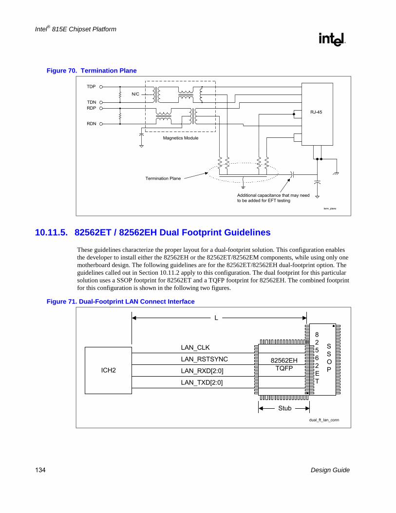
Intel® 815E Chipset Platform
R
134 Design Guide
Figure 70. Termination Plane
N/C
RJ-45
Magnetics Module
RDP
RDN
TDP
TDN
Termination Plane
Additional capacitance that may needto be added for EFT testing
term_plane
10.11.5. 82562ET / 82562EH Dual Footprint Guidelines
These guidelines characterize the proper layout for a dual-footprint solution. This configuration enables the developer to install either the 82562EH or the 82562ET/82562EM components, while using only one motherboard design. The following guidelines are for the 82562ET/82562EH dual-footprint option. The guidelines called out in Section 10.11.2 apply to this configuration. The dual footprint for this particular solution uses a SSOP footprint for 82562ET and a TQFP footprint for 82562EH. The combined footprint for this configuration is shown in the following two figures.
Figure 71. Dual-Footprint LAN Connect Interface
dual_ft_lan_conn
ICH2
LAN_TXD[2:0]
LAN_RXD[2:0]
LAN_RSTSYNC
LAN_CLK
L
82562ET
SSOP
Stub
82562EHTQFP

Intel® 815E Chipset Platform
R
Design Guide 135
Figure 72. Dual-Footprint Analog Interface
dual_ft_AN_conn
MagneticsModule
TDP
RJ45
82562EH/82562ET
TDN
RDP
RDN
RJ11
TXP
TXN
Tip
Ring82562EHConfig.
82562ETConfig.
The following are additional guidelines for this configuration:
• L = 1.5” to 4.5”
• Stub < 0.5”
• Either 82562EH or 82562ET/82562EM can be installed, but not both.
• 82562ET pins 28,29, and 30 overlap with 82562EH pins 17,18, and 19.
• Overlapping pins are tied to ground.
• No other signal pads should overlap or touch.
• Signal lines LAN_CLK, LAN_RSTSYNC, LAN_RXD[0], LAN_TXD[0], RDP, RDN, RXP/Ring, and RXN/Tip are shared by the 82562EH and 82562ET configurations.
• No stubs should be present when 82562ET is installed.
• Packages used for the dual footprint are TQFP for 82562EH and SSOP for 82562ET.
• A 22-Ω resistor can be placed at the driving side of the signal line to improve signal quality on the LAN connect interface.
• Resistor should be placed as close as possible to the component.
• Use components that can satisfy both the 82562ET and 82562EH configurations (i.e., magnetics module).
• Install components for either the 82562ET or the 82562EH configuration. Only one configuration can be installed at a time.
• Route shared signal lines such that stubs are not present or are kept to a minimum.
• Stubs may occur on shared signal lines (i.e RDP and RDN). These stubs are due to traces routed to an uninstalled component.
• Use 0-Ω resistors to connect and disconnect circuitry not shared by both configurations. Place resistor pads along the signal line to reduce stub lengths.
Intel® 815E Chipset Platform
R
136 Design Guide
10.12. LPC/FWH
10.12.1. In-Circuit FWH Programming
All cycles destined for the FWH will appear on the PCI. The ICH2 hub interface-to-PCI Bridge puts all processor boot cycles out on the PCI (before sending them out on the FWH interface). If the ICH2 is set for subtractive decode, these boot cycles can be accepted by a positive decode agent out on PCI. This enables booting from a PCI card that positively decodes these memory cycles. To boot from a PCI card, it is necessary to keep the ICH2 in the subtractive decode mode. If a PCI boot card is inserted and the ICH2 is programmed for positive decode, two devices will positively decode the same cycle. In systems with the 82380AB (ISA bridge), it is also necessary to keep the NOGO signal asserted when booting from a PCI ROM. Note that it is not possible to boot from a ROM behind the 82380AB. Once you have booted from the PCI card, you potentially could program the FWH in circuit and program the ICH2 CMOS.
10.12.2. FWH Vpp Design Guidelines
The Vpp pin on the FWH is used for programming the flash cells. The FWH supports a Vpp of 3.3 V or 12 V. If Vpp is 12 V, the flash cells will program about 50% faster than at 3.3 V. However, the FWH only supports 12 Vpp for 80 hours. The 12 Vpp would be useful in a programmer environment that is typically an event that occurs very infrequently (much less than 80 hours). The VPP pin MUST be tied to 3.3 V on the motherboard.

Intel® 815E Chipset Platform
R
Design Guide 137
11. Clocking For an Intel® 815 chipset-based system, there are two clock specifications. One is for a two-DIMM solution, and the other is for a three-DIMM solution.
11.1. 2-DIMM Clocking
11.1.1. Clock Generation Table 30. Intel CK815 (2-DIMM) Clocks
Number Clock Frequency
3 processor clocks 66/100/133 MHz
9 SDRAM clocks 100 MHz
7 PCI clocks 33 MHz
2 APIC clocks 16.67/33 MHz
2 48-MHz clocks 48 MHz
3 3-V, 66-MHz clocks 66 MHz
1 REF clock 14.31818 MHz
Features (56-pin SSOP package) • 9 copies of 100-MHz SDRAM clocks (3.3 V) [SDRAM0…7, DClk]
• 7 copies of PCI clock (33 MHz ) (3.3 V)
• 2 copies of APIC clock @ 33 MHz, synchronous to processor clock (2.5 V)
• 1 copy of 48-MHz USB clock (3.3 V) (non-SSC) (type 3 buffer)
• 1 copy of 48-MHz DOT clock (3.3 V) (non-SSC) (see DOT details)
• 3 copies of 3-V, 66-MHz clock (3.3 V)
• 1 copy of REF clock @ 14.31818 MHz (3.3 V)
• Ref. 14.31818-MHz xtal oscillator input
• Power-down pin
• Spread-spectrum support
• IIC support for turning off unused clocks

Intel® 815E Chipset Platform
R
138 Design Guide
11.1.2. 2-DIMM Clock Architecture
Figure 73. Intel® 815 Chipset Clock Architecture
Intel®815
chipsetGMCH
CPU 2_ITPAPIC 0CPU 1CPU 0
2.5 V
Clock Synthesizer
PWRDWN#SEL1SEL0
SDataSClk
SDRAM(0)SDRAM(1)SDRAM(2)SDRAM(3)
SDRAM(4)SDRAM(5)SDRAM(6)SDRAM(7)
DCLK
3V66 0
DOT
3V66 1
REF
PCI 0 / ICH
USB
3.3 V
APIC 12.5 V
PCI 1
PCI 2PCI 3PCI 4PCI 5PCI 6PCI 7
3.3 V
52555049
322928
3031
46454342
40393736
34
7
26
8
1
11
25
54
12
131516181920
MainMemory2 DIMMs
AGP
Data
Address
Control
Host unit
Graphics Memoryunit
Hub
Dot clock
ITP Processor
ICH2 32.768kHz
SIO
PCI total of 6devices (µATX)5 slots + 1 down
clk_arch_2DIMM
14.318 MHz
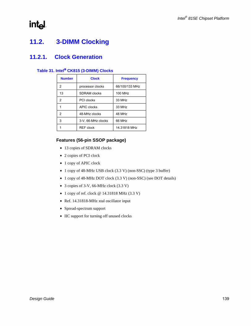
Intel® 815E Chipset Platform
R
Design Guide 139
11.2. 3-DIMM Clocking
11.2.1. Clock Generation
Table 31. Intel CK815 (3-DIMM) Clocks
Number Clock Frequency
2 processor clocks 66/100/133 MHz
13 SDRAM clocks 100 MHz
2 PCI clocks 33 MHz
1 APIC clocks 33 MHz
2 48-MHz clocks 48 MHz
3 3-V, 66-MHz clocks 66 MHz
1 REF clock 14.31818 MHz
Features (56-pin SSOP package) • 13 copies of SDRAM clocks
• 2 copies of PCI clock
• 1 copy of APIC clock
• 1 copy of 48-MHz USB clock (3.3 V) (non-SSC) (type 3 buffer)
• 1 copy of 48-MHz DOT clock (3.3 V) (non-SSC) (see DOT details)
• 3 copies of 3-V, 66-MHz clock (3.3 V)
• 1 copy of ref. clock @ 14.31818 MHz (3.3 V)
• Ref. 14.31818-MHz xtal oscillator input
• Spread-spectrum support
• IIC support for turning off unused clocks

Intel® 815E Chipset Platform
R
140 Design Guide
11.2.2. 3-DIMM Clock Architecture
Figure 74. Intel® 815 Chipset Clock Architecture
GMCH
APICCPU 1CPU 0
2.5 V
CK 815 3D
3V66 AGP
SDRAM(0)SDRAM(1)SDRAM(2)SDRAM(3)
SDRAM(4)SDRAM(5)SDRAM(6)SDRAM(7)
SDRAM(8)SDRAM(9)
SDRAM(10)SDRAM(11)
SDRAM(12)
3V66 03V66 1
DOT
USB
REF 0 14.3 MHz
PCI 0 / ICHPCI 1
15354
12
515047
46
45424138
29
10
26
4
1516
Main Memory3 DIMMs
AGP /local memory
Host I/F
AGIP /local
memory
GFXDotCLK
Hub link66/266
Processor
ICH2
SIO
PCI 1 tozero delay
Systemmemory
clk_arch_3DIMM
37363332
11
27
PCI slots/ down
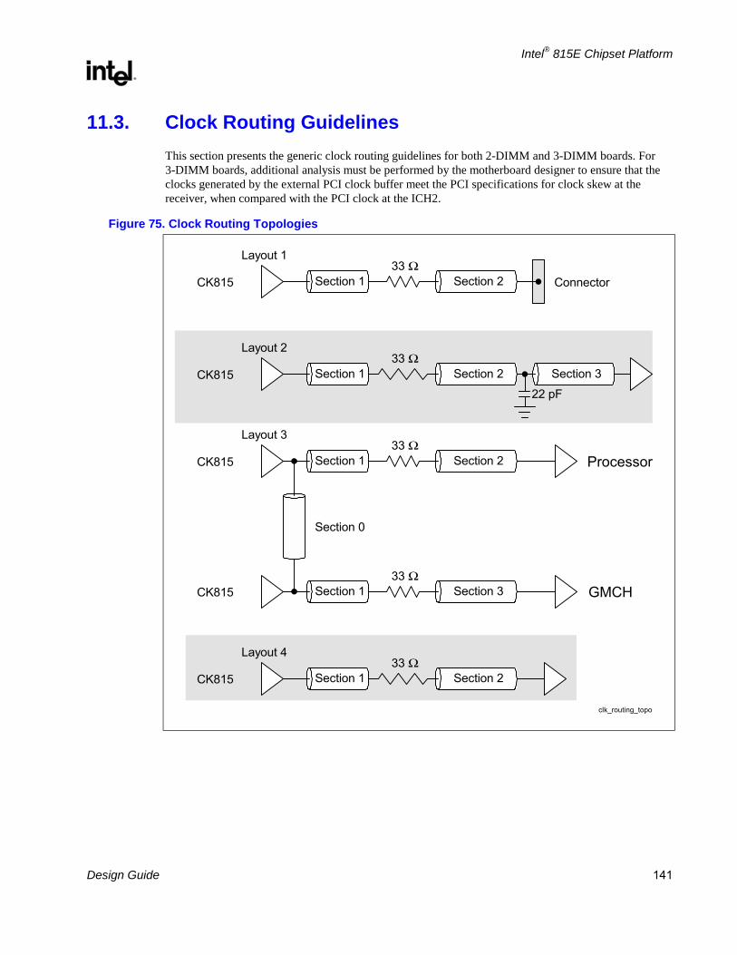
Intel® 815E Chipset Platform
R
Design Guide 141
11.3. Clock Routing Guidelines This section presents the generic clock routing guidelines for both 2-DIMM and 3-DIMM boards. For 3-DIMM boards, additional analysis must be performed by the motherboard designer to ensure that the clocks generated by the external PCI clock buffer meet the PCI specifications for clock skew at the receiver, when compared with the PCI clock at the ICH2.
Figure 75. Clock Routing Topologies
CK815 Section 1 Section 2
Layout 133 Ω
Connector
CK815 Section 1 Section 2
Layout 333 Ω
CK815 Section 1 Section 333 Ω
Section 0
Processor
GMCH
clk_routing_topo
CK815 Section 1 Section 2
Layout 433 Ω
CK815 Section 1 Section 2
Layout 233 Ω
Section 322 pF
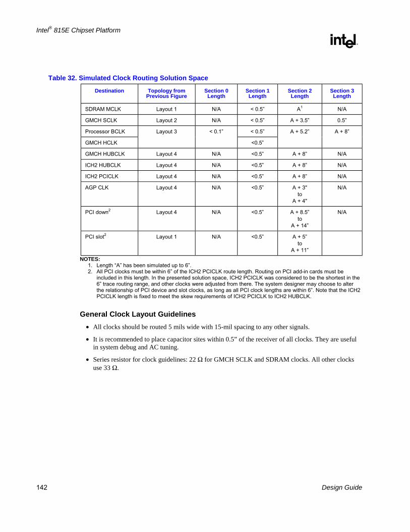
Intel® 815E Chipset Platform
R
142 Design Guide
Table 32. Simulated Clock Routing Solution Space
Destination Topology from Previous Figure
Section 0 Length
Section 1 Length
Section 2 Length
Section 3 Length
SDRAM MCLK Layout 1 N/A < 0.5 A1 N/A
GMCH SCLK Layout 2 N/A < 0.5 A + 3.5 0.5
Processor BCLK < 0.5
GMCH HCLK
Layout 3 < 0.1
<0.5
A + 5.2 A + 8
GMCH HUBCLK Layout 4 N/A <0.5 A + 8 N/A
ICH2 HUBCLK Layout 4 N/A <0.5 A + 8 N/A
ICH2 PCICLK Layout 4 N/A <0.5 A + 8 N/A
AGP CLK Layout 4 N/A <0.5 A + 3" to
A + 4"
N/A
PCI down2 Layout 4 N/A <0.5 A + 8.5 to
A + 14
N/A
PCI slot2 Layout 1 N/A <0.5 A + 5 to
A + 11
NOTES: 1. Length A has been simulated up to 6. 2. All PCI clocks must be within 6 of the ICH2 PCICLK route length. Routing on PCI add-in cards must be
included in this length. In the presented solution space, ICH2 PCICLK was considered to be the shortest in the 6 trace routing range, and other clocks were adjusted from there. The system designer may choose to alter the relationship of PCI device and slot clocks, as long as all PCI clock lengths are within 6. Note that the ICH2 PCICLK length is fixed to meet the skew requirements of ICH2 PCICLK to ICH2 HUBCLK.
General Clock Layout Guidelines • All clocks should be routed 5 mils wide with 15-mil spacing to any other signals.
• It is recommended to place capacitor sites within 0.5” of the receiver of all clocks. They are useful in system debug and AC tuning.
• Series resistor for clock guidelines: 22 Ω for GMCH SCLK and SDRAM clocks. All other clocks use 33 Ω.

Intel® 815E Chipset Platform
R
Design Guide 143
Clock Decoupling
Several general layout guidelines should be followed when laying out the power planes for the CK815 clock generator, as follows:
• Isolate power planes to the each of the clock groups.
• Place local decoupling as close as possible to power pins, and connect with short, wide traces and copper.
• Connect pins to appropriate power plane with power vias (larger than signal vias).
• Bulk decoupling should be connected to a plane with 2 or more power vias.
• Minimize clock signal routing over plane splits.
• Do not route any signals underneath the clock generator on the component side of the board.
• An example signal via is a 14-mil finished hole with a 24-mil to 26-mil path. An example power via is an 18-mil finished hole with a 33-mil to 38-mil path. For large decoupling or power planes with large current transients, a larger power via is recommended.
11.4. Clock Driver Frequency Strapping A CK-815-compliant clock driver device uses two of its pins to determine whether processor clock outputs should run at 133 MHz , 100 MHz or 66 MHz. The pin names are SEL0 and REF0. In addition, a third strapping pin is defined (SEL1), which must be pulled High for normal clock driver operation. Refer to the appropriate CK-815 clock driver specification for detailed strap timings and the logic encoding of straps.
SEL0 and REF0 are driven by either the processor, which depends on the processor populated in the 370-pin socket, or pull-up resistors on the motherboard. While SEL0 is a pure input to a CK-815-compliant clock driver, REF0 is also the 14-MHz output that drives the ICH2 and other devices on the platform. In addition to sampling straps at reset, CK-815-compliant clock drivers are configured by the BIOS via a two-wire interface to drive SDRAM clock outputs at either 100 MHz (default) or 133 MHz (if all system requirements are met).
If ACPI power management is supported on an Intel® 815 chipset platform, the motherboard designer should power the clock chip and input straps from the 3.3-Vsus (e.g., active in S0, S1, S3, S4, S5) power supply. This enables the clock driver to seamlessly maintain its configuration register settings while switching between ACPI sleep and wake states. The following figure shows the block diagram of the recommended clock frequency strapping network, with implementation considerations.
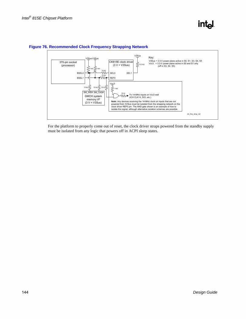
Intel® 815E Chipset Platform
R
144 Design Guide
Figure 76. Recommended Clock Frequency Strapping Network
370-pin socket(processor)
BSEL0
BSEL1
SEL0
REF0
SEL1
SM_WE# SM_CAS#
V3Sus V3Sus
1 kΩ 1 kΩ10 kΩ
10 kΩ
10 kΩ 10 kΩ 33 Ω
GMCH systemmemory I/F
(3 V = V3Sus)
CK815E clock driver(3 V = V3Sus)
Vcc3
1 kΩ
33 ΩTo 14-MHz inputs on Vcc3 well(ICH CLK14, SIO, etc.)
Note: Any devices receiving the 14-MHz clock on inputs that are notpowered from 3VSus must be isolated from the strapping network on theclock driver REF0 pin. The AND gate shown is an example of how toisolate this signal, although alternative isolation schemes are possible.
V3Sus
8.2 kΩ
Key:V3Sus = 3.3-V power plane active in S0, S1, S3, S4, S5Vcc3 = 3.3-V power plane active in S0 and S1 only (off in S3, S4, S5)
clk_freq_strap_net
For the platform to properly come out of reset, the clock driver straps powered from the standby supply must be isolated from any logic that powers off in ACPI sleep states.

Intel® 815E Chipset Platform
R
Design Guide 145
12. Power Delivery The following figure shows the power delivery architecture for an example Intel® 815E chipset platform. This power delivery architecture supports the “Instantly Available PC Design Guidelines” via the suspend-to-RAM (STR) state.
During STR, only the necessary devices are powered. These devices include: main memory, the ICH2 resume well, PCI wake devices (via 3.3 Vaux), AC’97, and optionally USB. (USB can be powered only if sufficient standby power is available.) To ensure that enough power is available during STR, a thorough power budget should be completed. The power requirements should include each device’s power requirements, both in suspend and in full-power. The power requirements should be compared with the power budget supplied by the power supply. Due to the requirements of main memory and the PCI 3.3 Vaux (and possibly other devices in the system), it is necessary to create a dual power rail.
The solutions in this Design Guide are only examples. Many power distribution methods achieve the similar results. When deviating from these examples, it is critical to consider the effect of a change.

Intel® 815E Chipset Platform
R
146 Design Guide
Figure 77. Power Delivery Map
Core: VCC_VID: 2.0V15.6A S0, S1
Intel® 815E ChipsetPlatform Power Map
VTT: 1.5 V ± 0.135 V2.7 A S0, S1
VCC3: 3 V ± 0.165 V15 mA S0, S1
VRM
ProcessorFan
-12 VSerial xceivers-5: 5 V ± 0.25 V30 mA S0, S1
Serial xceivers-12: 12 V ± 1.2 V22 mA S0, S1
Serial xceivers-N12: -12 V ± 1.2 V28 mA S0, S1
Serial ports
Intel® 815E chipset
VTT regulator
Display cache: 3.3 V ± 0.3 V960 mA S0, S1
USB cable power: 5 V ± 0.25 V1 A S0, S1
CK815-3.3: 3.3 V ± 0.165 V280 mA S0, S1
CK815-2.5: 2.5 V ± 0.125 V100 mA S0, S1
CLK
2.5 V regulator
1.8 V regulator
AC'97
3.3 VSB regulator
ATX P/Swith 720 mA
5 VSB± 5%
12 V± 5%
3.3 V± 5%
5 V± 5%
-12 V± 10%
LPC super I/O: 3.3V ±0.3V50 mA S0, S1
PS/2 keyboard/mouse 5 V ± 0.5 V1 A S0, S1
Super I/O
2 DIMM slots: 3.3 VSB ± 0.3 V4.8 A S0, S1; 64 mA S3
(3) PCI 3.3 Vaux: 3.3 VSB ± 0.3 V1.125 A S0, S1; 60 mA S3, S5
82559 LAN down 3.3 VSB ± 0.3 V195 mA S0,S1; 120 mA S3, S5
PCI
5 V dualswitch
5V_D
UAL
GMCH: 3.3 VSB ± 0.165 V110 mA S3, S5
GMCH core: 1.8 V ± 3%1.40 A S0, S1
GMCH: 3.3 V ± 0.165 V1.40 A S0, S1
FWH core: 3.3 V ± 0.3 V67 mA S0, S1
ICH2 resume: 3.3 VSB ± 0.3 V1.5 mA S0, S1; 300 µA S3, S5
ICH2 RTC: 3.3 VSB ± 0.3 V5 µA S0, S1, S3, S5
ICH2 core: 3.3 V ± 0.3 V300 mA S0, S1
ICH2 hub I/O: 1.8 V ± 0.09 V55 mA S0, S1
pwr_del_map
AC'97 3.3 VSB: 3.3 VSB ± 0.165 V150 mA S3, S5
AC'97 12V: 12 V ± 0.6 V 500 mA S0, S1
AC'97 -12 V: -12 V ± 1.2 V100 mA S0, S1
AC'97 5 V: 5 V ± 0.25 V1.00 A S0,S1
AC'97 5 VSB: 5 VSB ± 0.25 V500 mA S0, S1
AC'97 3.3 V: 3.3 V ± 0.165 V1.00 A S0,S1
Core: VCC_VID: 1.65 V17.2 A S0, S1
Core: VCC_VID: 2.0 V17.8 A S0, S1
Notes:Shaded regulators / components are ON in S3 and S5.KB / mouse will not support STR.Total max. power dissipation for GMCH = 4 W.Total max. power dissipation for AC'97 = 15 W.
VDDQ regulator GMCH VDDQ2.0 A S0, S1
12.1. Thermal Design Power Thermal Design power (TDP) is defined as the estimated maximum possible expected power generated in a component by a realistic application. It is based on extrapolations in both hardware and software technology over the life of the product. It does not represent the expected power generated by a power virus.
The TDP of the 82815 GMCH component is5.1W.
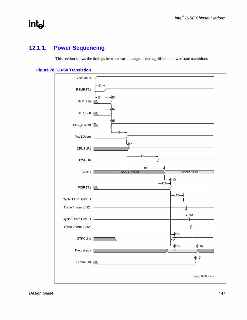
Intel® 815E Chipset Platform
R
Design Guide 147
12.1.1. Power Sequencing
This section shows the timings between various signals during different power state transitions.
Figure 78. G3-S0 Transistion
Clocks invalid Clocks valid
t17
t16t15
t14
t13
t12
t10t11
t9
t8
t7
t6
t5
t4
t3t2
t1
Vcc3.3sus
RSMRST#
SLP_S3#
SLP_S5#
SUS_STAT#
Vcc3.3core
CPUSLP#
PWROK
Clocks
PCIRST#
Cycle 1 from GMCH
Cycle 1 from ICH2
Cycle 2 from GMCH
Cycle 2 from ICH2
STPCLK#
Freq straps
CPURST#
pwr_G3-S0_trans

Intel® 815E Chipset Platform
R
148 Design Guide
Figure 79. S0-S3-S0 Transition
DRAM active DRAM in STR (CKE low) DRAM active
Clocks valid Clocks invalid Clocks valid
t16t15
t9
t22
t8
t23t21
t17
t13
t12
t11t20
t19
t7t18
t24
Vcc3.3sus
RSMRST#
STPCLK#
Stop grant cycle
CPUSLP#
Go_C3 from ICH
Ack_C3 from GMCH
DRAM
SUS_STAT#
PCIRST#
Cycle 1 from GMCH
Cycle 1 from ICH2
Cycle 2 from GMCH
Cycle 2 from ICH2
CPURST#
SLP_S3#
SLP_S5#
PWROK
Vcc3.3core
Clocks
Freq straps
Wake event
pwr_S0-S3-S0_trans

Intel® 815E Chipset Platform
R
Design Guide 149
Figure 80. S0-S5-S0 Transition
DRAM active DRAM in STR (CKE low) DRAM active
Clocks valid Clocks invalid Clocks valid
t16t15
t9
t22
t8
t26t25
t23t21
t17
t13
t12
t11t20
t19
t7t18
t24
Vcc3.3sus
RSMRST#
STPCLK#
Stop grant cycle
CPUSLP#
Go_C3 from ICH
Ack_C3 from GMCH
DRAM
SUS_STAT#
PCIRST#
Cycle 1 from GMCH
Cycle 1 from ICH2
Cycle 2 from GMCH
Cycle 2 from ICH2
CPURST#
SLP_S3#
SLP_S5#
PWROK
Vcc3.3core
Clocks
Freq straps
Wake event
pwr_S0-S5-S0_trans

Intel® 815E Chipset Platform
R
150 Design Guide
Table 33. Power Sequencing Timing Definitions
Symbol Parameter Min. Max. Units
t1 VccSUS good to RSMRST# inactive 1 25 ms
t2 VccSUS good to SLP_S3#, SLP_S5#, and PCIRST# active 50 ns
t3 RSMRST# inactive to SLP_S3# inactive 1 4 RTC clocks
t4 RSMRST# inactive to SLP_S5# inactive 1 4 RTC clocks
t5 RSMRST# inactive to SUS_STAT# inactive 1 4 RTC clocks
t6 SLP_S3#, SLP_S5#, SUS_STAT# inactive to Vcc3.3core good
* *
t7 Vcc3.3core good to CPUSLP# inactive 50 ns
t8 Vcc3.3core good to PWROK active * *
t9 Vcc3.3core good to clocks valid * *
t10 Clocks valid to PCIRST# inactive 500 µs
t11 PWROK active to PCIRST# inactive .9 1.1 ms
t12 PCIRST# inactive to cycle 1 from GMCH 1 ms
t13 Cycle 1 from ICH2 to cycle 2 from GMCH 60 ns
t14 PCIRST# inactive to STPCLK de-assertion 1 4 PCI clocks
t15 PCIRST# to frequency straps valid -4 4 PCI clocks
t16 Cycle 2 from ICH2 to frequency straps invalid 180 ns
t17 Cycle 2 from ICH2 to CPURST# inactive 110 ns
t18 Stop Grant Cycle to CPUSLP# active 8 PCI clocks
t19 CPUSLP# active to SUS_STAT# active 1 RTC clock
t20 SUS_STAT# active to PCIRST# active 2 3 RTC clocks
t21 PCIRST# active to SLP_S3# active 1 2 RTC clocks
t22 PWROK inactive to Vcc3.3core not good 20 ns
t23 Wake event to SLP_S3# inactive 2 3 RTC clocks
t24 PCIRST# inactive to STPCLK# inactive 1 4 PCI clocks
t25 SLP_S3# active to SLP_S5# active 1 2 RTC clocks
t26 SLP_S5# inactive to SLP_S3# inactive 2 3 RTC clocks

Intel® 815E Chipset Platform
R
Design Guide 151
12.2. Pull-up and Pull-down Resistor Values The pull-up and pull-down values are system dependent. The appropriate value for a system can be determined from an AC/DC analysis of the pull-up voltage used, the current drive capability of the output driver, the input leakage currents of all devices on the signal net, the pull-up voltage tolerance, the pull-up/pull-down resistor tolerance, the input high-voltage/low-voltage specifications, the input timing specifications (RC rise time), etc. Analysis should be performed to determine the minimum/maximum values usable on an individual signal. Engineering judgment should be used to determine the optimal value. This determination can include cost concerns, commonality considerations, manufacturing issues, specifications, and other considerations.
A simplistic DC calculation for a pull-up value is:
RMAX = (VccPU MIN - VIH MIN) / ILEAKAGE MAX
RMIN = (VccPU MAX - VIL MAX) / IOL MAX
Since ILEAKAGE MAX is normally very small, RMAX may not be meaningful. RMAX also is determined by the maximum allowable rise time. The following calculation allows for t, the maximum allowable rise time, and C, the total load capacitance in the circuit, including the input capacitance of the devices to be driven, the output capacitance of the driver, and the line capacitance. This calculation yields the largest pull-up resistor allowable to meet the rise time t.
RMAX = -t / (C * In(1-(VIH MIN / VccPU MIN) ) )
Figure 81. Pull-up Resistor Example
Vccpu min.
Rmax
VIH min.ILeakage max.
Vccpu max.
Rmin
VIL max.IOL max.
pwr_pullup_res

Intel® 815E Chipset Platform
R
152 Design Guide
12.3. ATX Power Supply PWRGOOD Requirements The PWROK signal must be glitch free for proper power management operation. The ICH2 sets the PWROK_FLR bit (ICH2 GEN_PMCON_2, General PM Configuration 2 Register, PM-dev31: function 0, bit 0, at offset A2h). If this bit is set upon resume from S3 power-down, the system will reboot and control of the system will not be given to the program running when entering the S3 state. System designers should insure that PWROK signal designs are glitch free.
12.4. Power Management Signals • A power button is required by the ACPI specification.
• PWRBTN# is connected to the front panel on/off power button. The ICH2 integrates 16-ms debouncing logic on this pin.
• AC power loss circuitry has been integrated into the ICH2 to detect power failure.
• It is recommended that the PS_POK signal from the power supply connector be routed through a Schmitt trigger to square-off and maintain its signal integrity. It should not be connected directly to logic on the board.
• PS_POK logic from the power supply connector can be powered from the core voltage supply.
• RSMRST# logic should be powered by a standby supply, while making sure that the input to the ICH2 is at the 3-V level. The RSMST# signal requires a minimum time delay of 1 ms from the rising edge of the standby power supply voltage. A Schmitt trigger circuit is recommended to drive the RSMRST# signal. To provide the required rise time, the 1-ms delay should be placed before the Schmitt trigger circuit. The reference design implements a 20-ms delay at the input of the Schmitt trigger to ensure that the Schmitt trigger inverters have sufficiently powered up before switching the input. Also ensure that voltage on RSMRST# does not exceed VCC(RTC).
• It is recommended that 3.3-V logic be used to drive RSMRST# to alleviate rise time problems when using a resistor divider from VCC5.
• The PWROK signal to the chipset is a 3-V signal.
• The core well power valid to PWROK asserted at the chipset is a minimum of 1 ms.
• PWROK to the chipset must be deasserted after RSMRST#.
• PWRGOOD signal to processor is driven with an open-collector buffer pulled up to 2.5 V, using a 330-Ω resistor.
• RI# can be connected to the serial port if this feature is used. To implement ring indicate as a wake event, the RS232 transceiver driving the RI# signal must be powered when the ICH2 suspend well is powered. This can be achieved with a serial port transceiver powered from the standby well that implements a shutdown feature.
• SLP_S3# from the ICH2 must be inverted and then connected to PSON of the power supply connector to control the state of the core well during sleep states.
• For an ATX power supply, when PSON is Low, the core wells are turned on. When PSON is high, the core wells from the power supply are turned off.
Intel® 815E Chipset Platform
R
Design Guide 153
12.4.1. Power Button Implementation
The following items should be considered when implementing a power management model for a desktop system. The power states are as follows:
S1 – Stop Grant – (processor context not lost)
S3 - STR (Suspend to RAM)
S4 - STD (Suspend to Disk)
S5 - Soft-off
• Wake: Pressing the power button wakes the computer from S1-S5.
• Sleep: Pressing the power button signals software/firmware in the following manner:
• If SCI is enabled, the power button will generate an SCI to the OS. The OS will implement the power button policy to allow orderly shutdowns. Do not override this with additional hardware.
• If SCI is not enabled: Enable the power button to generate an SMI and go directly to soft-off or a supported sleep
state. Poll the power button status bit during POST while SMIs are not loaded and go directly to soft-
off if it gets set. Always install an SMI handler for the power button that operates until ACPI is enabled.
• Emergency Override: Pressing the power button for 4 seconds goes directly to S5. This is only to be used in EMERGENCIES when system is not responding. This will cause the user data to be lost in most cases.
• Do not promote pressing the power button for 4 seconds as the normal mechanism to power the machine off. This violates ACPI.
• To be compliant with the latest PC9x specification, machines must appear to the user to be off when in the S1-S4 sleeping states. This includes: All lights, except a power state light, must be off. The system must be inaudible: silent or stopped fan, drives off.
• Note: Contact Microsoft for the latest information concerning PC9x and Microsoft Logo programs.
12.4.2. 1.8V/3.3V Power Sequencing
The ICH2 has two pairs of associated 1.8V and 3.3V supplies. These are Vcc1_8, Vcc3_3 and VccSus1_8, VccSus3_3. These pairs are assumed to power up and power down together. The difference between the two associated supplies must never be greater than 2.0V. The 1.8V supply may come up before the 3.3V supply without violating this rule (though this is generally not practical in a desktop environment, since the 1.8V supply is typically derived from the 3.3V supply by means of a linear regulator).
One serious consequence of violation of this "2V Rule" is electrical overstress of oxide layers, resulting in component damage.
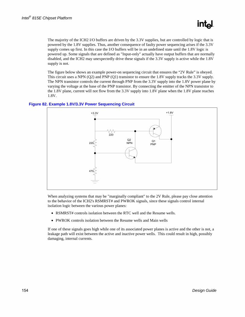
Intel® 815E Chipset Platform
R
154 Design Guide
The majority of the ICH2 I/O buffers are driven by the 3.3V supplies, but are controlled by logic that is powered by the 1.8V supplies. Thus, another consequence of faulty power sequencing arises if the 3.3V supply comes up first. In this case the I/O buffers will be in an undefined state until the 1.8V logic is powered up. Some signals that are defined as "Input-only" actually have output buffers that are normally disabled, and the ICH2 may unexpectedly drive these signals if the 3.3V supply is active while the 1.8V supply is not.
The figure below shows an example power-on sequencing circuit that ensures the “2V Rule” is obeyed. This circuit uses a NPN (Q2) and PNP (Q1) transistor to ensure the 1.8V supply tracks the 3.3V supply. The NPN transistor controls the current through PNP from the 3.3V supply into the 1.8V power plane by varying the voltage at the base of the PNP transistor. By connecting the emitter of the NPN transistor to the 1.8V plane, current will not flow from the 3.3V supply into 1.8V plane when the 1.8V plane reaches 1.8V.
Figure 82. Example 1.8V/3.3V Power Sequencing Circuit
Q1 PNP
Q2 NPN
220
220
470
+3.3V +1.8V
When analyzing systems that may be "marginally compliant" to the 2V Rule, please pay close attention to the behavior of the ICH2's RSMRST# and PWROK signals, since these signals control internal isolation logic between the various power planes:
• RSMRST# controls isolation between the RTC well and the Resume wells.
• PWROK controls isolation between the Resume wells and Main wells
If one of these signals goes high while one of its associated power planes is active and the other is not, a leakage path will exist between the active and inactive power wells. This could result in high, possibly damaging, internal currents.

Intel® 815E Chipset Platform
R
Design Guide 155
12.5. Power Plane Splits
Figure 83. Power Plane Split Example
pwr_plane_splits
12.6. Thermal Design Power The thermal design power is the estimated maximum possible expected power generated in a component by a realistic application. It is based on extrapolations in both hardware and software technology over the life of the product. It does not represent the expected power generated by a power virus.
The thermal design power for the ICH2 is 1.5 W ±15%.

Intel® 815E Chipset Platform
R
156 Design Guide
12.7. Glue Chip 3 (Intel® ICH2 Glue Chip) To reduce the component count and BOM cost of the ICH2 platform, Intel has developed an ASIC component that integrates miscellaneous platform logic into a single chip. The Glue Chip 3 is designed to integrate some or all of the following functions into a single device. By integrating much of the required glue logic into a single device, overall board cost can be reduced.
Features • PWROK signal generation
• Control circuitry for Suspend To RAM
• Power Supply power up circuitry
• RSMRST# generation
• Backfeed cutoff circuit for suspend to RAM
• 5V reference generation
• Flash FLUSH# / INIT# circuit
• HD single color LED driver
• IDE reset signal generation/PCIRST# buffers
• Voltage translation for Audio MIDI signal
• Audio-disable circuit
• Voltage translation for DDC to monitor
• Tri-state buffers for test
More information regarding this component is available from the following vendors.
Vendor Contact Contact Information
Fujitsu Microelectronics
Customer Response Center 3545 North 1st Street, M/S 104 San Jose, CA 95134-1804 phone: 1-800-866-8600 fax: 1-408-922-9179 email: [email protected]
Mitel Semiconductor Greg Kizik Regional Business Manager
1735 Technology Drive Suite 240 San Jose, CA 95110 phone: 408-451-4723 fax: 408-451-4710 e-mail: [email protected] http://www.mitelsemi.com

Intel® 815E Chipset Platform
R
Design Guide 157
13. System Design Checklist
13.1. Design Review Checklist
Introduction
This checklist highlights design considerations that should be reviewed prior to manufacturing a motherboard that implements an Intel® 815E chipset. This is not a complete list and does guarantee that a design will function properly. For items other than those in the following text, refer to the latest revision of the Design Guide for more-detailed instructions regarding motherboard design.
Design Checklist Summary
The following set of tables provides design considerations for the various portions of a design. Each table describes one of those portions and is titled accordingly. Contact your Intel Field Representative in the event of questions or issues regarding the interpretation of the information in these tables.
13.2. Processor Checklist
13.2.1. GTL Checklist Checklist Items Recommendations
A[35:3]# 1 Connect A[31:3]# to GMCH. Leave A[35:32]# as No Connect (not supported by chipset).
ADS#, BNR#, BPRI#, DBSY#, DEFER#, DRDY#, HA[31:3]#, HD[63:0]#, HIT#, HITM#, LOCK#, REQ[4:0]#, RS[2:0]#, TRDY#
Terminate to Vtt1.5 through 56 Ω resistor. Connect to GMCH.
BREQ[0]# (BR0#) 56 Ω pull-down resistor to ground
RESET#, RESET2# Terminate to Vtt1.5 through 86 Ω resistor, decoupled through 22 Ω resistor in series with 10 pF capacitor to ground. Connect to GMCH. Also terminated to Vtt1.5 through 86 Ω resistor.
13.2.2. CMOS Checklist Checklist Items Recommendations
IERR# 150 Ω pull-up resistor to VCCCMOS if tied to custom logic, or leave as No Connect (not used by chipset)
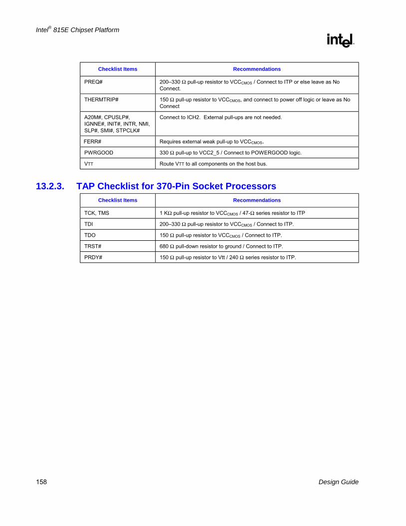
Intel® 815E Chipset Platform
R
158 Design Guide
Checklist Items Recommendations
PREQ# 200330 Ω pull-up resistor to VCCCMOS / Connect to ITP or else leave as No Connect.
THERMTRIP# 150 Ω pull-up resistor to VCCCMOS, and connect to power off logic or leave as No Connect
A20M#, CPUSLP#, IGNNE#, INIT#, INTR, NMI, SLP#, SMI#, STPCLK#
Connect to ICH2. External pull-ups are not needed.
FERR# Requires external weak pull-up to VCCCMOS. PWRGOOD 330 Ω pull-up to VCC2_5 / Connect to POWERGOOD logic.
VTT Route VTT to all components on the host bus.
13.2.3. TAP Checklist for 370-Pin Socket Processors Checklist Items Recommendations
TCK, TMS 1 KΩ pull-up resistor to VCCCMOS / 47-Ω series resistor to ITP
TDI 200330 Ω pull-up resistor to VCCCMOS / Connect to ITP.
TDO 150 Ω pull-up resistor to VCCCMOS / Connect to ITP.
TRST# 680 Ω pull-down resistor to ground / Connect to ITP.
PRDY# 150 Ω pull-up resistor to Vtt / 240 Ω series resistor to ITP.
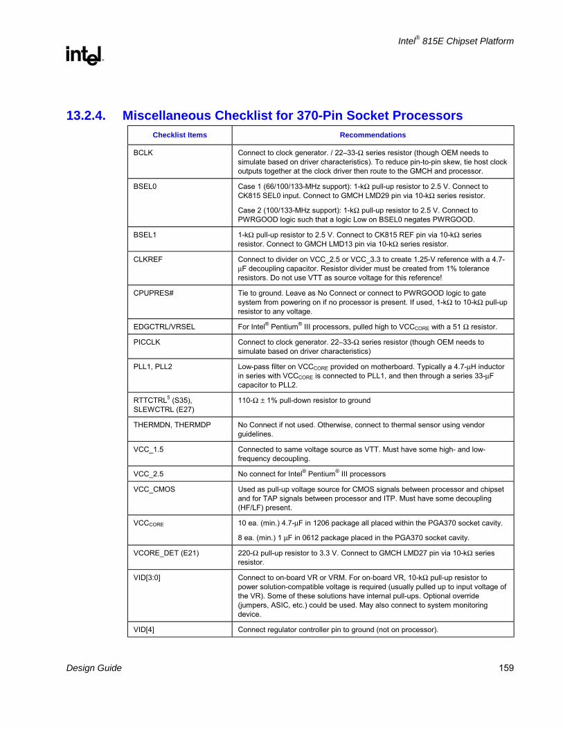
Intel® 815E Chipset Platform
R
Design Guide 159
13.2.4. Miscellaneous Checklist for 370-Pin Socket Processors Checklist Items Recommendations
BCLK Connect to clock generator. / 2233-Ω series resistor (though OEM needs to simulate based on driver characteristics). To reduce pin-to-pin skew, tie host clock outputs together at the clock driver then route to the GMCH and processor.
BSEL0 Case 1 (66/100/133-MHz support): 1-kΩ pull-up resistor to 2.5 V. Connect to CK815 SEL0 input. Connect to GMCH LMD29 pin via 10-kΩ series resistor.
Case 2 (100/133-MHz support): 1-kΩ pull-up resistor to 2.5 V. Connect to PWRGOOD logic such that a logic Low on BSEL0 negates PWRGOOD.
BSEL1 1-kΩ pull-up resistor to 2.5 V. Connect to CK815 REF pin via 10-kΩ series resistor. Connect to GMCH LMD13 pin via 10-kΩ series resistor.
CLKREF Connect to divider on VCC_2.5 or VCC_3.3 to create 1.25-V reference with a 4.7-µF decoupling capacitor. Resistor divider must be created from 1% tolerance resistors. Do not use VTT as source voltage for this reference!
CPUPRES# Tie to ground. Leave as No Connect or connect to PWRGOOD logic to gate system from powering on if no processor is present. If used, 1-kΩ to 10-kΩ pull-up resistor to any voltage.
EDGCTRL/VRSEL For Intel® Pentium® III processors, pulled high to VCCCORE with a 51 Ω resistor.
PICCLK Connect to clock generator. 2233-Ω series resistor (though OEM needs to simulate based on driver characteristics)
PLL1, PLL2 Low-pass filter on VCCCORE provided on motherboard. Typically a 4.7-µH inductor in series with VCCCORE is connected to PLL1, and then through a series 33-µF capacitor to PLL2.
RTTCTRL5 (S35), SLEWCTRL (E27)
110-Ω ± 1% pull-down resistor to ground
THERMDN, THERMDP No Connect if not used. Otherwise, connect to thermal sensor using vendor guidelines.
VCC_1.5 Connected to same voltage source as VTT. Must have some high- and low-frequency decoupling.
VCC_2.5 No connect for Intel® Pentium® III processors
VCC_CMOS Used as pull-up voltage source for CMOS signals between processor and chipset and for TAP signals between processor and ITP. Must have some decoupling (HF/LF) present.
VCCCORE 10 ea. (min.) 4.7-µF in 1206 package all placed within the PGA370 socket cavity.
8 ea. (min.) 1 µF in 0612 package placed in the PGA370 socket cavity.
VCORE_DET (E21) 220-Ω pull-up resistor to 3.3 V. Connect to GMCH LMD27 pin via 10-kΩ series resistor.
VID[3:0] Connect to on-board VR or VRM. For on-board VR, 10-kΩ pull-up resistor to power solution-compatible voltage is required (usually pulled up to input voltage of the VR). Some of these solutions have internal pull-ups. Optional override (jumpers, ASIC, etc.) could be used. May also connect to system monitoring device.
VID[4] Connect regulator controller pin to ground (not on processor).

Intel® 815E Chipset Platform
R
160 Design Guide
Checklist Items Recommendations
VREF [7:0] Connect to VREF voltage divider made up of 75-Ω and 150-Ω 1% resistors connected to Vtt.
Decoupling Guidelines:
4 ea. (min.) 0.1 µF in 0603 package placed within 500 mils of VREF pins
Vtt Connect AH20, AK16, AL13, AL21, AN11, AN15, and G35 to 1.5-V regulator. Provide high- and low-frequency decoupling.
Decoupling Guidelines:
19 ea (min.) 0.1 µF in 0603 package placed within 200 mils of AGTL+ termination resistor packs (r-paks). Use one capacitor for every two (r-paks).
4 ea (min.) 0.47 µF in 0612 package
NO CONNECTS The following pins must be left as no-connects: AK30, AM2, F10, L33, N33, N35, N37, Q33, Q35, Q37, R2, W35, X2, Y1
AA33, AA35, AN21, E23, S33, S37, U35, U37
A platform using an Intel® 815E chipset is not compatible with an Intel® Celeron processor (PPGA). These pins must be connected directly to Vtt.
G37 No Connect
13.3. GMCH Checklist
13.3.1. AGP Interface 1X Mode Checklist Checklist Items Recommendations
RBF#, WBF#, PIPE#, GREQ#, GGNT#, GPAR, GFRAME#, GIRDY#, GTRDY#, GSTOP#, GDEVSEL#, GPERR#, GSERR# , ADSTB0, ADSTB1, SBSTB
Pull up to VDDQ through 8.2 kΩ
ADSTB0#, ADSTB1#, SBSTB#
Pull down to ground through 8.2 kΩ
PME# Connect to PCI connector 0 device Ah. / Connect to PCI connector 1 device Bh. / Connect to 82559 LAN (if implemented).
TYPEDET# Connect to AGP voltage regulator circuitry / AGP reference circuitry.
PIRQ#A, PIRQ#B Pull up to 5 V through 2.7 kΩ. / Follow ref. schematics (other device connections).
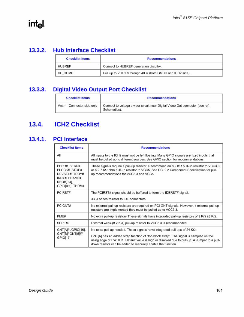
Intel® 815E Chipset Platform
R
Design Guide 161
13.3.2. Hub Interface Checklist Checklist Items Recommendations
HUBREF Connect to HUBREF generation circuitry.
HL_COMP Pull up to VCC1.8 through 40 Ω (both GMCH and ICH2 side).
13.3.3. Digital Video Output Port Checklist Checklist Items Recommendations
VREF Connector side only Connect to voltage divider circuit near Digital Video Out connector (see ref. Schematics).
13.4. ICH2 Checklist
13.4.1. PCI Interface Checklist Items Recommendations
All All inputs to the ICH2 must not be left floating. Many GPIO signals are fixed inputs that must be pulled up to different sources. See GPIO section for recommendations.
PERR#, SERR# PLOCK#, STOP# DEVSEL#, TRDY# IRDY#, FRAME# REQ#[0:4], GPIO[0:1], THRM#
These signals require a pull-up resistor. Recommend an 8.2 KΩ pull-up resistor to VCC3.3 or a 2.7 KΩ ohm pull-up resistor to VCC5. See PCI 2.2 Component Specification for pull-up recommendations for VCC3.3 and VCC5.
PCIRST# The PCIRST# signal should be buffered to form the IDERST# signal.
33 Ω series resistor to IDE connectors.
PCIGNT# No external pull-up resistors are required on PCI GNT signals. However, if external pull-up resistors are implemented they must be pulled up to VCC3.3.
PME# No extra pull-up resistors These signals have integrated pull-up resistors of 9 KΩ ±3 KΩ.
SERIRQ External weak (8.2 KΩ) pull-up resistor to VCC3.3 is recommended.
GNT[A]# /GPIO[16], GNT[B]/ GNT[5]#/ GPIO[17]
No extra pull-up needed. These signals have integrated pull-ups of 24 KΩ.
GNT[A] has an added strap function of top block swap. The signal is sampled on the rising edge of PWROK. Default value is high or disabled due to pull-up. A Jumper to a pull-down resistor can be added to manually enable the function.
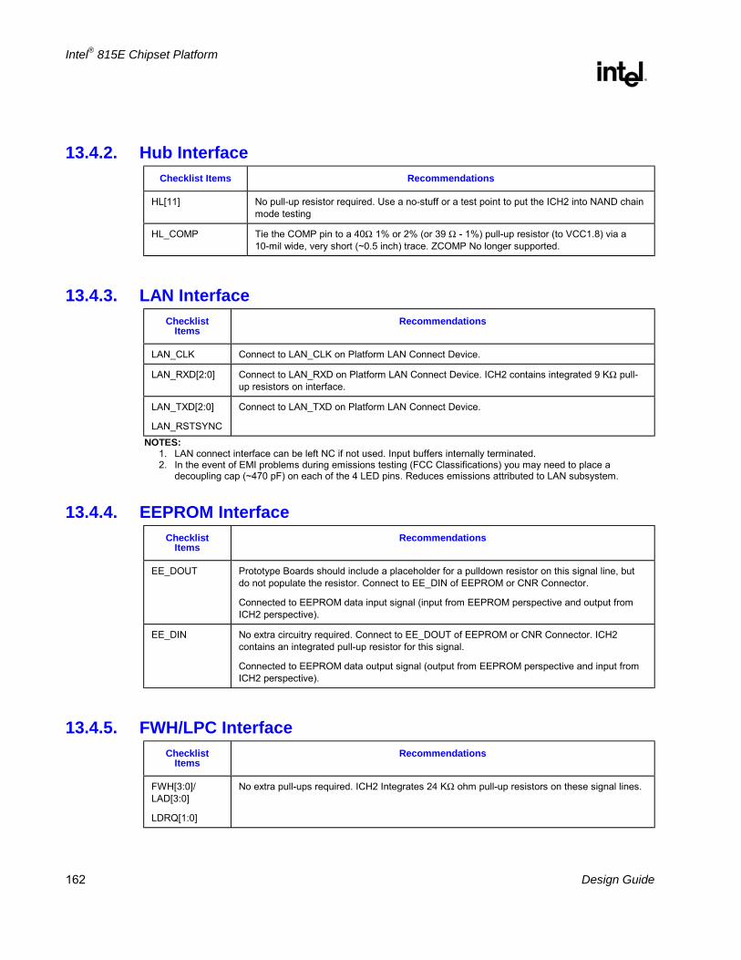
Intel® 815E Chipset Platform
R
162 Design Guide
13.4.2. Hub Interface Checklist Items Recommendations
HL[11] No pull-up resistor required. Use a no-stuff or a test point to put the ICH2 into NAND chain mode testing
HL_COMP Tie the COMP pin to a 40Ω 1% or 2% (or 39 Ω - 1%) pull-up resistor (to VCC1.8) via a 10-mil wide, very short (~0.5 inch) trace. ZCOMP No longer supported.
13.4.3. LAN Interface Checklist
Items Recommendations
LAN_CLK Connect to LAN_CLK on Platform LAN Connect Device.
LAN_RXD[2:0] Connect to LAN_RXD on Platform LAN Connect Device. ICH2 contains integrated 9 KΩ pull-up resistors on interface.
LAN_TXD[2:0]
LAN_RSTSYNC
Connect to LAN_TXD on Platform LAN Connect Device.
NOTES: 1. LAN connect interface can be left NC if not used. Input buffers internally terminated. 2. In the event of EMI problems during emissions testing (FCC Classifications) you may need to place a
decoupling cap (~470 pF) on each of the 4 LED pins. Reduces emissions attributed to LAN subsystem.
13.4.4. EEPROM Interface Checklist
Items Recommendations
EE_DOUT Prototype Boards should include a placeholder for a pulldown resistor on this signal line, but do not populate the resistor. Connect to EE_DIN of EEPROM or CNR Connector.
Connected to EEPROM data input signal (input from EEPROM perspective and output from ICH2 perspective).
EE_DIN No extra circuitry required. Connect to EE_DOUT of EEPROM or CNR Connector. ICH2 contains an integrated pull-up resistor for this signal.
Connected to EEPROM data output signal (output from EEPROM perspective and input from ICH2 perspective).
13.4.5. FWH/LPC Interface Checklist
Items Recommendations
FWH[3:0]/ LAD[3:0]
LDRQ[1:0]
No extra pull-ups required. ICH2 Integrates 24 KΩ ohm pull-up resistors on these signal lines.

Intel® 815E Chipset Platform
R
Design Guide 163
13.4.6. Interrupt Interface Checklist
Items Recommendations
PIRQ#[D:A] These signals require a pull-up resistor. The recommendation is a 2.7 KΩ pull-up resistor to VCC5 or 8.2 KΩ to VCC3.3.
In Non-APIC Mode the PIRQx# signals can be routed to interrupts 3, 4, 5, 6, 7, 9, 10, 11, 12, 14 or 15 as described in the Interrupt Steering section. Each PIRQx# line has a separate Route Control Register.
In APIC mode, these signals are connected to the internal I/O APIC in the following fashion: PIRQ[A]# is connected to IRQ16, PIRQ[B]# to IRQ17, PIRQ[C]# to IRQ18, and PIRQ[D]# to IRQ19. This frees the ISA interrupts.
PIRQ#[G:F]/ GPIO[4:3]
These signals require a pull-up resistor. Recommend a 2.7 KΩ pull-up resistor to VCC5 or 8.2 KΩ to VCC3.3.
In Non-APIC Mode the PIRQx# signals can be routed to interrupts 3, 4, 5, 6, 7, 9, 10, 11, 12, 14 or 15 as described in the Interrupt Steering section. Each PIRQx# line has a separate Route Control Register.
In APIC mode, these signals are connected to the internal I/O APIC in the following fashion: PIRQ[E]# is connected to IRQ20, PIRQ[F]# to IRQ21, PIRQ[G]# to IRQ22, and PIRQ[H]# to IRQ23. This frees the ISA interrupts.
PIRQ#[H]
PIRQ#[E]
These signals require a pull-up resistor. Recommend a 2.7 KΩ pull-up resistor to VCC5 or 8.2 KΩ to VCC3.3.
Since PIRQ[H]# and PIRQ[E]# are used internally for LAN and USB controllers, they cannot be used as GPIO(s) pin.
APIC If the APIC is used:
150 Ω pull-up resistors on APICD[0:1]
Connect APICCLK to CK133 with a 2033 Ω series termination resistor.
If the APIC is not used on UP systems:
The APICCLK can either be tied to GND or connected to CK133, but not left floating.
Pull APICD[0:1] to GND through 10 KΩ pull-down resistors.
Use pull-downs for each APIC signal. Do not share resistor to pull signals up.
13.4.7. GPIO Checklist Checklist Items Recommendations
All Ensure ALL unconnected signals are OUTPUTS ONLY!
GPIO[7:0] These pins are in the Main Power Well. Pull-ups must use the VCC3.3 plane. Unused core well inputs must be pulled up to VCC3.3. These signals are 5V tolerant.
GPIO[1:0] can be used as REQ[A:B]#. GPIO[1] can also used as PCI REQ[5]#.
[13:11], GPIO[8] These pins are in the Resume Power Well. Pull-ups must use the VCCSUS3.3 plane. These are the only GPI signals in the resume well with associated status bits in the GPE1_STS register. Unused resume well inputs must be pulled up to VCCSUS3.3. These signals are not 5V tolerant.
These are the only GPIs that can be used as ACPI compliant wake events.
GPIO[23:16] Fixed as output only. Can be left NC. In Main Power Well. GPIO22 is open drain.
GPIO[24,25,27,28] These I/O pins can be NC. These pins are in the resume power well.

Intel® 815E Chipset Platform
R
164 Design Guide
13.4.8. USB Checklist Items Recommendations
USBP[3:0]P
USBP[3:0]N
See Figure 1 for circuitry needed on each differential Pair.
VCC USB (Cable power)
It should be powered from the 5V core instead of the 5V standby, unless adequate standby power is available.
Voltage drop considerations
The resistive component of the fuses, ferrite beads and traces must be considered when choosing components, and power and GND trace widths. Minimize the resistance between the Vcc5 power supply and the USB ports to prevent voltage drop.
Sufficient bypass capacitance should be located near the USB receptacles to minimize the voltage drop that occurs during the hot plugging a new device. For more information, see the USB specification.
Fuse A fuse larger than 1A can be chosen to minimize the voltage drop.
Figure 84. USB Data Line Schematic
15 kΩ
15 kΩ
15 Ω
15 Ω
ICH2
P+
P-
< 1"
< 1"
45 Ω
45 Ω
Driver
Driver
Transmission line
Motherboard trace
Motherboard trace
usb_data_line_schem
USB
con
nect
or
90 Ω
USB twisted-pair cable
Optional47 pf
Optional47 pf
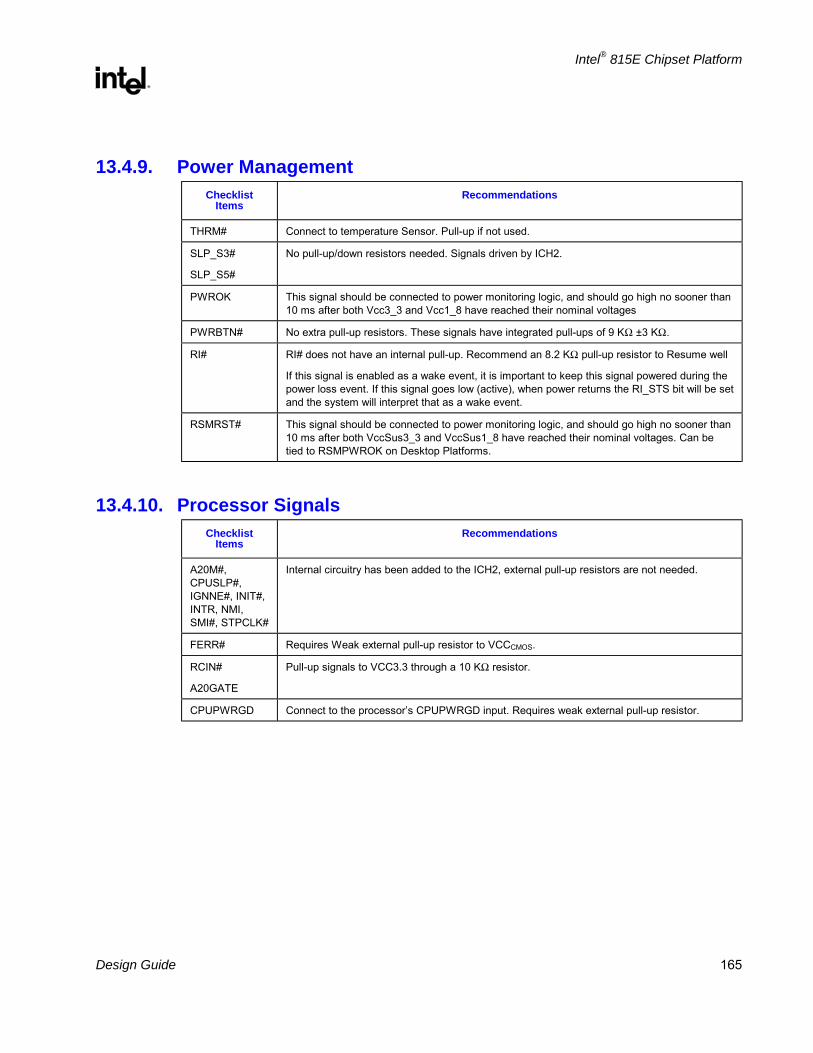
Intel® 815E Chipset Platform
R
Design Guide 165
13.4.9. Power Management Checklist
Items Recommendations
THRM# Connect to temperature Sensor. Pull-up if not used.
SLP_S3#
SLP_S5#
No pull-up/down resistors needed. Signals driven by ICH2.
PWROK This signal should be connected to power monitoring logic, and should go high no sooner than 10 ms after both Vcc3_3 and Vcc1_8 have reached their nominal voltages
PWRBTN# No extra pull-up resistors. These signals have integrated pull-ups of 9 KΩ ±3 KΩ.
RI# RI# does not have an internal pull-up. Recommend an 8.2 KΩ pull-up resistor to Resume well
If this signal is enabled as a wake event, it is important to keep this signal powered during the power loss event. If this signal goes low (active), when power returns the RI_STS bit will be set and the system will interpret that as a wake event.
RSMRST# This signal should be connected to power monitoring logic, and should go high no sooner than 10 ms after both VccSus3_3 and VccSus1_8 have reached their nominal voltages. Can be tied to RSMPWROK on Desktop Platforms.
13.4.10. Processor Signals Checklist
Items Recommendations
A20M#, CPUSLP#, IGNNE#, INIT#, INTR, NMI, SMI#, STPCLK#
Internal circuitry has been added to the ICH2, external pull-up resistors are not needed.
FERR# Requires Weak external pull-up resistor to VCCCMOS.
RCIN#
A20GATE
Pull-up signals to VCC3.3 through a 10 KΩ resistor.
CPUPWRGD Connect to the processors CPUPWRGD input. Requires weak external pull-up resistor.
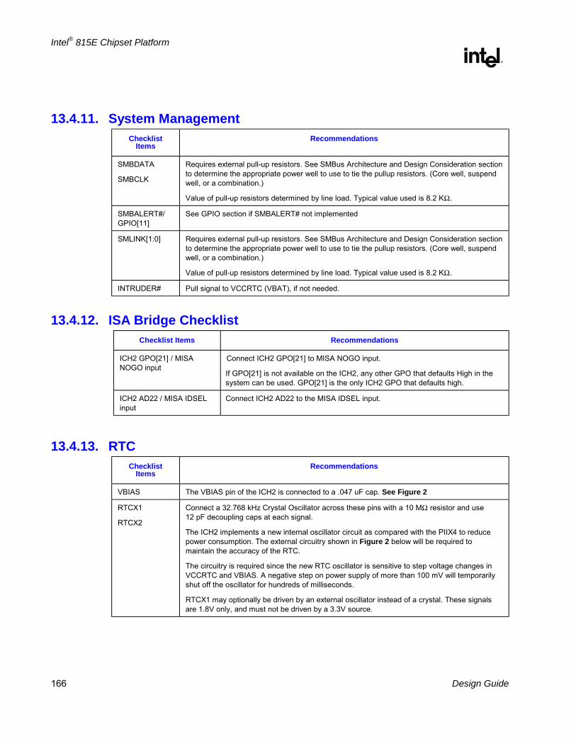
Intel® 815E Chipset Platform
R
166 Design Guide
13.4.11. System Management Checklist
Items Recommendations
SMBDATA
SMBCLK
Requires external pull-up resistors. See SMBus Architecture and Design Consideration section to determine the appropriate power well to use to tie the pullup resistors. (Core well, suspend well, or a combination.)
Value of pull-up resistors determined by line load. Typical value used is 8.2 KΩ.
SMBALERT#/ GPIO[11]
See GPIO section if SMBALERT# not implemented
SMLINK[1:0] Requires external pull-up resistors. See SMBus Architecture and Design Consideration section to determine the appropriate power well to use to tie the pullup resistors. (Core well, suspend well, or a combination.)
Value of pull-up resistors determined by line load. Typical value used is 8.2 KΩ.
INTRUDER# Pull signal to VCCRTC (VBAT), if not needed.
13.4.12. ISA Bridge Checklist Checklist Items Recommendations
ICH2 GPO[21] / MISA NOGO input
Connect ICH2 GPO[21] to MISA NOGO input.
If GPO[21] is not available on the ICH2, any other GPO that defaults High in the system can be used. GPO[21] is the only ICH2 GPO that defaults high.
ICH2 AD22 / MISA IDSEL input
Connect ICH2 AD22 to the MISA IDSEL input.
13.4.13. RTC Checklist
Items Recommendations
VBIAS The VBIAS pin of the ICH2 is connected to a .047 uF cap. See Figure 2
RTCX1
RTCX2
Connect a 32.768 kHz Crystal Oscillator across these pins with a 10 MΩ resistor and use 12 pF decoupling caps at each signal.
The ICH2 implements a new internal oscillator circuit as compared with the PIIX4 to reduce power consumption. The external circuitry shown in Figure 2 below will be required to maintain the accuracy of the RTC.
The circuitry is required since the new RTC oscillator is sensitive to step voltage changes in VCCRTC and VBIAS. A negative step on power supply of more than 100 mV will temporarily shut off the oscillator for hundreds of milliseconds.
RTCX1 may optionally be driven by an external oscillator instead of a crystal. These signals are 1.8V only, and must not be driven by a 3.3V source.
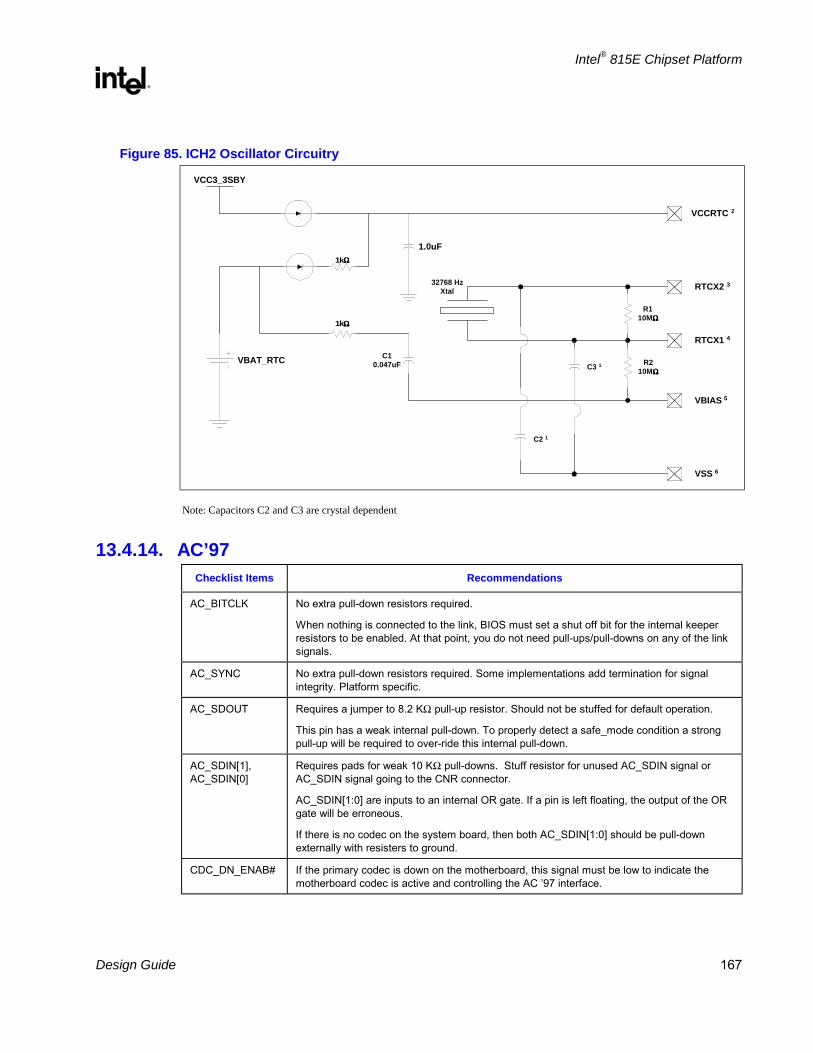
Intel® 815E Chipset Platform
R
Design Guide 167
Figure 85. ICH2 Oscillator Circuitry
32768 HzXtal
C10.047uF
C2 1
C3 1
R110MΩΩΩΩ
R210MΩΩΩΩ
VCCRTC 2
RTCX2 3
RTCX1 4
VBIAS 5
VSS 6
VCC3_3SBY
VBAT_RTC
1.0uF
1kΩΩΩΩ
1kΩΩΩΩ
Note: Capacitors C2 and C3 are crystal dependent
13.4.14. AC’97 Checklist Items Recommendations
AC_BITCLK No extra pull-down resistors required.
When nothing is connected to the link, BIOS must set a shut off bit for the internal keeper resistors to be enabled. At that point, you do not need pull-ups/pull-downs on any of the link signals.
AC_SYNC No extra pull-down resistors required. Some implementations add termination for signal integrity. Platform specific.
AC_SDOUT Requires a jumper to 8.2 KΩ pull-up resistor. Should not be stuffed for default operation.
This pin has a weak internal pull-down. To properly detect a safe_mode condition a strong pull-up will be required to over-ride this internal pull-down.
AC_SDIN[1], AC_SDIN[0]
Requires pads for weak 10 KΩ pull-downs. Stuff resistor for unused AC_SDIN signal or AC_SDIN signal going to the CNR connector.
AC_SDIN[1:0] are inputs to an internal OR gate. If a pin is left floating, the output of the OR gate will be erroneous.
If there is no codec on the system board, then both AC_SDIN[1:0] should be pull-down externally with resisters to ground.
CDC_DN_ENAB# If the primary codec is down on the motherboard, this signal must be low to indicate the motherboard codec is active and controlling the AC 97 interface.

Intel® 815E Chipset Platform
R
168 Design Guide
13.4.15. Miscellaneous Signals Checklist
Items Recommendations
SPKR No extra pull-up resistors. Has integrated pull-up of between 18 KΩ and 42 KΩ. The integrated pull-up is only enabled at boot/reset for strapping functions; at all other times, the pull-up is disabled.
A low effective impedance may cause the TCO Timer Reboot function to be erroneously disabled.
Effective Impedance due Speaker and Codec circuitry must be greater than 50 KΩ or a means to isolate the resistive load from the signal while PWROK is low be found. see following figure.
TP[0] Requires external pull-up resistor to VCCSUS3.3
FS[0] Rout to a testpoint. ICH2 contains an integrated pull-up for this signal. Testpoint used for manufacturing appears in XOR tree.
Figure 86. SPKR Circuitry
Speaker_Circuit
Stuff jumper todisable time-outfeature.
R < 7.3 kΩReff > 50 kΩ
Effective Impedencedue to speaker andcodec circuit.
18 kΩ - 42 kΩ
Integrated Pull-up
3.3V
ICH2
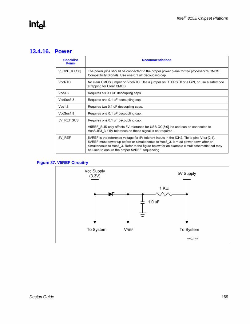
Intel® 815E Chipset Platform
R
Design Guide 169
13.4.16. Power Checklist
Items Recommendations
V_CPU_IO[1:0] The power pins should be connected to the proper power plane for the processor 's CMOS Compatibility Signals. Use one 0.1 uF decoupling cap.
VccRTC No clear CMOS jumper on VccRTC. Use a jumper on RTCRST# or a GPI, or use a safemode strapping for Clear CMOS
Vcc3.3 Requires six 0.1 uF decoupling caps
VccSus3.3 Requires one 0.1 uF decoupling cap.
Vcc1.8 Requires two 0.1 uF decoupling caps.
VccSus1.8 Requires one 0.1 uF decoupling cap.
5V_REF SUS Requires one 0.1 uF decoupling cap.
V5REF_SUS only affects 5V-tolerance for USB OC[3:0] ins and can be connected to VccSUS3_3 if 5V tolerance on these signal is not required.
5V_REF 5VREF is the reference voltage for 5V tolerant inputs in the ICH2. Tie to pins VREF[2:1]. 5VREF must power up before or simultaneous to Vcc3_3. It must power down after or simultaneous to Vcc3_3. Refer to the figure below for an example circuit schematic that may be used to ensure the proper 5VREF sequencing.
Figure 87. V5REF Circuitry
Vcc Supply(3.3V) 5V Supply
To SystemVREFTo System
1 KΩ
1.0 uF
vref_circuit

Intel® 815E Chipset Platform
R
170 Design Guide
13.4.17. IDE Checklist Checklist
Items Recommendations
PDD[15:0], SDD[15:0]
No extra series termination resistors or other pull-ups/pull-downs are required. These signals have integrated series resistors. NOTE: Simulation data indicates that the integrated series termination resistors can range from 31 ohms to 43 ohms.
PDD7/SDD7 does not require a 10 KΩ pull-down resistor. Refer to ATA ATAPI-4 specification.
PDIOW#, PDIOR#, PDDACK#, PDA[2:0], PDCS1#, PDCS3#, SDIOW#, SDIOR#, SDDACK#, SDA[2:0], SDCS1#, SDCS3#
No extra series termination resistors. Pads for series resistors can be implemented should the system designer have signal integrity concerns. These signals have integrated series resistors. NOTE: Simulation data indicates that the integrated series termination resistors can range from 31 ohms to 43 ohms.
PDREQ
SDREQ
No extra series termination resistors. No pull-down resistors needed.
These signals have integrated series resistors in the ICH2. These signals have integrated pull-down resistors in the ICH2.
PIORDY
SIORDY
No extra series termination resistors. These signals have integrated series resistors in the ICH2. Pull-up to VCC3.3 via a 4.7 KΩ resistor.
IRQ14, IRQ15 Recommend 8.2 KΩ10 KΩ pull-up resistors to VCC3.3.
No extra series termination resistors.
IDERST# The PCIRST# signal should be buffered to form the IDERST# signal. A 33 ohm series termination resistor is recommended on this signal.
Cable Detect: Host Side/Device Side Detection:
Connect IDE pin PDIAG/CBLID to an ICH2 GPIO pin. Connect a 10 KΩ resistor to GND on the signal line. The 10 KΩ resistor to GND prevents GPI from floating if no devices are present on either IDE interface. Allows use of 3.3V and 5V tolerant GPIOs.
Device Side Detection:
Connect a 0.047 µF capacitor from IDE pin PDIAG/CBLID to GND. No ICH2 connection. NOTE: All ATA66/ATA100 drives will have the capability to detect cables
Note: The maximum trace length from the ICH2 to the ATA connector is 8 inches.

Intel® 815E Chipset Platform
R
Design Guide 171
Figure 88. Host/Device Side Detection Circuitry
80-conductorIDE cable
IDE drive
5 V
ICH2
GPIO
GPIO
Open
IDE drive
5 V
40-conductorcable
IDE drive
5 V
PDIAG#ICH2
GPIO
GPIO
IDE drive
5 V
PDIAG#
PDIAG#PDIAG#
10 kΩ
10 kΩ
To secondaryIDE connector
To secondaryIDE connector
PDIAG#/CBLID#
PDIAG#/CBLID#
10 kΩ
10 kΩ
10 kΩ
10 kΩ
IDE_combo_cable_det
Figure 89. Device Side Only Cable Detection
80-conductorIDE cable
IDE drive
5 V
ICH2
Open
IDE drive
5 V
40-conductorcable
IDE drive
5 V
PDIAG#ICH2
IDE drive
5 V
PDIAG#
PDIAG#PDIAG#PDIAG#/CBLID#
PDIAG#/CBLID#
10 kΩ
10 kΩ
10 kΩ
10 kΩ
IDE_dev_cable_det
0.047 µF
0.047 µF

Intel® 815E Chipset Platform
R
172 Design Guide
13.5. LPC Checklist
Checklist Items Recommendations
RCIN# Pull up through 8.2-kΩ resistor to Vcc3_3.
LPC_PME# Pull up through 8.2-kΩ resistor to Vcc3_3. Do not connect LPC PME# to PCI PME#. If the design requires the Super I/O to support wake from any suspend state, connect Super I/O LPC_PME# to a resume well GPI on the ICH2.
LPC_SMI# Pull up through 8.2-kΩ resistor to Vcc3_3. This signal can be connected to any ICH2 GPI. The GPI_ROUTE register provides the ability to generate an SMI# from a GPI assertion.
TACH1, TACH2 Pull up through 4.7-kΩ resistor to Vcc3_3.
Jumper for decoupling option (decouple with 0.1-µF cap)
J1BUTTON1, JPBUTTON2, J2BUTTON1, J2BUTTON2
Pull up through 1-kΩ resistor to Vcc5. Decouple through 47-pF cap to GND.
LDRQ#1 Pull up through 4.7-kΩ resistor to Vcc3SBY.
A20GATE Pull up through 8.2-kΩ resistor to Vcc3_3.
MCLK, MDAT Pull up through 4.7-kΩ resistor to PS2V5.
L_MCLK, L_MDAT Decoupled using 470-pFcap to ground.
RI#1_C, CTS0_C, RXD#1_C, RXD0_C, RI0_C, DCD#1_C, DSR#1_C, DSR0_C, DTR#1_C, DTR0_C, DCD0_C, RTS#1_C, RTS0_C, CTS#1_C, TXD#1_C, TXD0_C
Decoupled using 100-pF cap to GND.
L_SMBD Pass through 150-Ω resistor to 82559.
SERIRQ Pull up through 8.2 kΩ to Vcc3_3.
SLCT#, PE, BUSY, ACK#, ERROR#
Pull up through 2.2-kΩ resistor to Vcc5_DB25_DR.
Decouple through 180-pF cap to GND.
LFRAME# No required pull-up resistor
LDRQ#0 No required pull-up resistor
STROBE#, ALF#, SLCTIN#, PAR_INIT#
Signal passes through a 33-Ω resistor and is pulled up through a 2.2-kΩ resistor to Vcc5_DB25_CR. Decoupled using a 180-pF cap to GND.
PWM1, PWM2 Pull up to 4.7 kΩ to Vcc3_3 and connected to jumper for decouple with 0.1-µF cap to GND.
INDEX#, TRK#0, RDATA#, DSKCHG#, WRTPRT#
Pull up through 1-kΩ resistor to Vcc5.
PDR0, PDR1, PDR2, PDR3, PDR4, PDR5, PDR6, PDR7
Passes through 33-Ω resistor.
Pull up through 2.2 kΩ to Vcc5_DB5_CRD and couple through 180-pF cap to GND.
SYSOPT Pull down with 4.7-kΩ resistor to GND or IO address of 0x02E.
Intel® 815E Chipset Platform
R
Design Guide 173
13.6. System Checklist Checklist Items Recommendations
KEYLOCK# Pull up through 10-kΩ resistor to Vcc3_3.
PBTN_IN Connects to PBSwitch and PBin.
PWRLED Pull up through a 220-Ω resistor to Vcc5.
R_IRTX Signal IRTX after it is pulled down through 4.7-kΩ resistor to GND and passes through 82-Ω resistor.
IRRX Pull up to 100-kΩ resistor to Vcc3_3.
When signal is input for SI/O decouple through 470-pF cap to GND
IRTX Pull down through 4.7 kΩ to GND.
Signal passes through 82-Ω resistor.
When signal is input to SI/O decouple through 470-pF cap to GND
FP_PD Decouple through a 470-pF cap. To GND.
Pull up 470 Ω to Vcc5.
PWM1, PWM2 Pull up through a 4.7-kΩ resistor to Vcc3_3.
13.7. FWH Checklist Checklist Items Recommendations
No floating inputs Unused FGPI pins must be tied to a valid logic level.
WPROT, TBLK_LCK Pull up through a 4.7-kΩ resistor to Vcc3_3.
R_VPP Pulled up to Vcc3_3 and decoupled with two 0.1-µF caps to GND.
FGPI0_PD, FGPI1_PD, FGPI2_PD, FPGI3_PD, FPGI4_PD, IC_PD
Pull down through a 8.2-kΩ resistor to GND.
FWH_ID1, FWH_ID2, FWH_ID3 Pull down to GND.
INIT# FWH INIT# must be connected to processor INIT#.
RST# FWH RST# must be connected to PCIRST#.
ID[3:0] For a system with only one FWH device, tie ID[3:0] to ground.
Intel® 815E Chipset Platform
R
174 Design Guide
13.8. Clock Synthesizer Checklist Checklist Items Recommendations
REFCLK Connects to R-RefCLK, USB_CLK, SIO_CLK14, and ICHCLK14.
ICH_3V66/3V66_0, DOTCLK Passes through 33-Ω resistor.
When signal is input for ICH, it is pulled down through a 18-pF cap to GND.
DCLK/DCLK_WR Passes through 33-Ω resistor.
When signal is input for GMCH, it is pulled down through a 22-pF cap to GND.
CPUHCLK/CPU_0_1 Passes through 33-Ω resistor.
When signal is input for 370PGA, decouple through a 18-pF cap to GND.
R_REFCLK REFCLK passed through 10-kΩ resistor.
When signal is input for 370PGA, pull up through 1-kΩ resistor to Vcc3_3 and pass through 10-kΩ resistor.
USB_CLK, ICH_CLK14 REFCLK passed through 10-Ω resistor.
XTAL_IN, XTAL_OUT Passes through 14.318-MHz oscillator.
Pulled down through 18-pF cap to GND.
SEL1_PU Pulled up via MEMV3 circuitry through 8.2-kΩ resistor.
FREQSEL Connected to clock frequency selection circuitry through 10-kΩ resistor. (See CRB schematic, page 4.)
L_VCC2_5 Connects to VDD2_5[01] through ferrite bead to Vcc2_5.
GMCHHCLK/CPU_1, ITPCLK/CPU_2, PCI_0/PCLK_OICH, PCI_1/PCLK_1, PCI_2/PCLK_2, PCI_3/PCLK_3, PCI_4/PCLK_4, PCI_5/PCLK_5, PCI_6/PCLK_6, APICCLK_CPU/APIC_0, APICCLK)ICH/APIC_1, USBCLK/USB_0, GMCH_3V66/3V66_1, AGPCLK_CONN
Passes through 33-Ω resistor.
MEMCLK0/DRAM_0, MEMCLK1/DRAM_1, MEMCLK2/DRAM_2, MEMCLK3/DRAM_3, MEMCLK4/DRAM_4, MEMCLK5/DRAM_5, MEMCLK6/DRAM_6, MEMCLK7/DRAM_7, SCLK
Pass through 22-Ω resistor.

Intel® 815E Chipset Platform
R
Design Guide 175
13.9. ITP Probe Checklist Checklist Items Recommendations
R_TCK, TCK R_TMS, TMS Connect to 370-Pin socket through 47-Ω resistor and pull up to VCMOS.
ITPRDY#, R_ITPRDY# Connect to 370-Pin socket through 243-Ω resistor.
TDI Pull up through 330-Ω resistor to VCMOS.
TDO Pull up through 150-Ω resistor to VCMOS.
PLL1 See Design Guide.
PLL2 See Design Guide.
13.10. System Memory Checklist Checklist Items Recommendations
SM_CSA#[0:3, SM_CSB#[3:0, SMAA[11:8,3:0], SM_MD[0:63], SM_CKE[0:3], S_DQM[0:7]
Connect from GMCH to DIMM0, DIMM1.
SM_MAA[7:4], SM_MAB[7:4]# Connect from GMCH to DIMM0, DIMM1 through 10-Ω resistors.
SM_CAS# Connected to R_REFCLK through 10-kΩ resistor.
SM_RAS# Jumpered to GND through 10-kΩ resistor.
SM_WE# Connected to R_BSEL0# through 10-kΩ resistor.
CKE[50] (For 3-DIMM implementation)
When implementing a 3-DIMM configuration, all six CKE signals on the GMCH are used. (0,1 for DIMM0; 2, 3 for DIMM1; 4,5 for DIMM2)
REGE Connect to GND (since the Intel® 815E chipset does not support registered DIMMs).
WP(Pin 81 on the DIMMS) Add a 4.7-kΩ pull-up resistor to 3.3 V. This recommendation write-protects the DIMMs EEPROM.
SRCOMP Needs a 60-Ω resistor pulled up to 3.3 V.

Intel® 815E Chipset Platform
R
176 Design Guide
13.11. Power Delivery Checklist Checklist Items Recommendations
All voltage regulator components meet maximum current requirements.
Consider all loads on a regulator, including other regulators.
All regulator components meet thermal requirements.
Ensure the voltage regulator components and dissipate the required amount of heat.
VCC1_8 VCC1_8 power sources must supply 1.85 V and be between (1.795 V to 1.905 V).
If devices are powered directly from a dual rail (i.e., not behind a power regulator), then the RDSon of the FETs used to create the dual rail must be analyzed to ensure there is not too much voltage drop across the FET.
Dual voltage rails may not be at the expected voltage.
Dropout voltage The minimum dropout for all voltage regulators must be considered. Take into account that the voltage on a dual rail may not be the expected voltage.
Voltage tolerance requirements are met. See the individual component specifications for each voltage tolerance.
Total power consumption in S3 must be less than the rated standby supply current.
Adequate power must be supplied by power supply.

Intel® 815E Chipset Platform
R
Design Guide 177
14. Third-Party Vendor Information This design guide has been compiled to give an overview of important design considerations while providing sources for additional information. This chapter includes information regarding various third-party vendors who provide products to support the Intel 815 chipset. The list of vendors can be used as a starting point for the designer. Intel does not endorse any one vendor, nor guarantee the availability or functionality of outside components. Contact the manufacturer for specific information regarding performance, availability, pricing and compatibility.
Super I/O (Vendors Contact Phone) • SMSC Dave Jenoff (909) 244-4937 • Natiobnal Semiconductor Robert Reneau (408) 721-2981 • ITE Don Gardenhire (512)388-7880 • Winbond James Chen (02) 27190505 - Taipei office
Clock Generation (Vendors Contact Phone) • Cypress Semiconductor John Wunner 206-821-9202 x325 • ICS Raju Shah 408-925-9493 • IMI Elie Ayache 408-263-6300, x235 • PERICOM Ken Buntaran 408-435-1000
Memory Vendors
http://developer.intel.com/design/motherbd/se/se_mem.htm
Voltage Regulator Vendors (Vendors Contact Phone)
• Linear Tech Corp. Stuart Washino 408-432-6326 • Celestica Dariusz Basarab 416-448-5841 • Corsair Microsystems John Beekley 888-222-4346 • Delta Electronics Colin Weng 886-2-6988, x233(Taiwan) • N. America: Delta Products Corp. Maurice Lee 510-770-0660, x111
Flat Panel (Vendors Contact Phone) • Silicon Images Inc Vic Dacosta 408-873-3111
GPA (a.k.a. AIMM) Card (Vendors Contact Phone)
• Kingston TBD • Smart Modular TBD • Micron Semiconductor TBD

Intel® 815E Chipset Platform
R
178 Design Guide
This page is intentionally left blank.
Intel® 815E Chipset Platform
R
Design Guide 179
Appendix A: Customer Reference Board (CRB)
This section provides a set of schematics for the Intel® 815E chipset’s Customer Reference Board (CRB).

Intel® 815E Chipset Platform
R
180 Design Guide
This page is intentionally left blank.
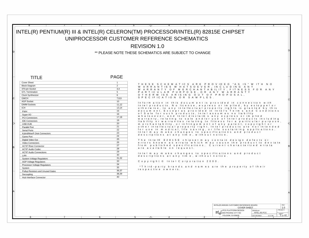
COVER SHEET
TITLE
1
PAGE
** PLEASE NOTE THESE SCHEMATICS ARE SUBJECT TO CHANGE
UNIPROCESSOR CUSTOMER REFERENCE SCHEMATICSREVISION 1.0
INTEL(R) PENTIUM(R) III & INTEL(R) CELERON(TM) PROCESSOR/INTEL(R) 82815E CHIPSET
B
C
D
8 7 6 5 4 3 2 1
D
C
B
A
345678
A
2 1OFFOLSOM, CA 95630
1900 PRAIRIE CITY RD
PROJECT:
REV:
DRAWN BY:
SHEET:LAST REVISED:
PCG PLATFORM DESIGNINTEL (R) PCG
42
1.0INTEL(R) 82815E CUSTOMER REFERENCE BOARD
R
12-17-99
Cover Sheet
Block Diagram
GTL Termination370-pin Socket
Clock Synthesizer
GMCHAGP Socket
DIMM Sockets
FWH
Super I/O
USB HUB
PCI Connectors
Parallel Port
Digital Video OutVideo Connectors
AC'97 Riser Connector
AC'97 Audio CodecAC'97 Audio Connections
LANSystem Voltage Regulators
System
Pullup Resistors and Unused Gates
1
2
3,45
6
7,8,910
21
22
2324
25
2627
2829
33
IDE Connectors
Serial Ports
Game Port
Kybrd/Mse/F.Disk Connectors
30
31,32
Processor Voltage Regulators
AGP Voltage Regulators34
3536,37
11,12
13,1415
1617,18
20
19
38,39
40
ICH
Hub Interface ConnectorDecoupling
T H E S E S C H E M A T I C S A R E P R O V I D E D “ A S I S ” W I T H N OW A R R A N T I E S W H A T S O E V E R , I N C L U D I N G A N YW A R R A N T Y O F M E R C H A N T A B I L I T Y , F I T N E S S F O R A N YP A R T I C U L A R P U R P O S E , O R A N Y W A R R A N T YO T H E R W I S E A R I S I N G O U T O F P R O P O S A L ,S P E C I F I C A T I O N O R S A M P L E S .
I n f o r m a t i o n i n t h i s d o c u m e n t i s p r o v i d e d i n c o n n e c t i o n w i t hI n t e l p r o d u c t s . N o l i c e n s e , e x p r e s s o r i m p l i e d , b y e s t o p p e l o ro t h e r w i s e , t o a n y i n t e l l e c t u a l p r o p e r t y r i g h t s i s g r a n t e d b y t h i sd o c u m e n t . E x c e p t a s p r o v i d e d i n I n t e l ' s T e r m s a n d C o n d i t i o n so f S a l e f o r s u c h p r o d u c t s , I n t e l a s s u m e s n o l i a b i l i t yw h a t s o e v e r , a n d I n t e l d i s c l a i m s a n y e x p r e s s o r i m p l i e dw a r r a n t y , r e l a t i n g t o s a l e a n d / o r u s e o f I n t e l p r o d u c t s i n c l u d i n gl i a b i l i t y o r w a r r a n t i e s r e l a t i n g t o f i t n e s s f o r a p a r t i c u l a r p u r p o s e ,m e r c h a n t a b i l i t y , o r i n f r i n g e m e n t o f a n y p a t e n t , c o p y r i g h t o ro t h e r i n t e l l e c t u a l p r o p e r t y r i g h t . I n t e l p r o d u c t s a r e n o t i n t e n d e df o r u s e i n m e d i c a l , l i f e s a v i n g , o r l i f e s u s t a i n i n g a p p l i c a t i o n s .I n t e l m a y m a k e c h a n g e s t o s p e c i f i c a t i o n s a n d p r o d u c td e s c r i p t i o n s a t a n y t i m e , w i t h o u t n o t i c e .
T h e I n t e l ® 8 2 8 1 5 E c h i p s e t m a y c o n t a i n d e s i g n d e f e c t s o re r r o r s k n o w n a s e r r a t a w h i c h m a y c a u s e t h e p r o d u c t t o d e v i a t ef r o m p u b l i s h e d s p e c i f i c a t i o n s . C u r r e n t c h a r a c t e r i z e d e r r a t aa r e a v a i l a b l e o n r e q u e s t .
I n t e l m a y m a k e c h a n g e s t o s p e c i f i c a t i o n s a n d p r o d u c td e s c r i p t i o n s a t a n y t i m e , w i t h o u t n o t i c e .
C o p y r i g h t © I n t e l C o r p o r a t i o n 2 0 0 0 .
* T h i r d - p a r t y b r a n d s a n d n a m e s a r e t h e p r o p e r t y o f t h e i rr e s p e c t i v e o w n e r s .

BLOCK DIAGRAM
2
B
C
D
8 7 6 5 4 3 2 1
D
C
B
A
345678
A
2 1OFFOLSOM, CA 95630
1900 PRAIRIE CITY RD
PROJECT:
REV:
DRAWN BY:
SHEET:LAST REVISED:
PCG PLATFORM DESIGNINTEL (R) PCG
42
1.0INTEL(R) 82815E CUSTOMER REFERENCE BOARD
R
12-17-99
GMCH
Block Diagram
370-Pin Socket Processor
DA
TA
CT
RL
AD
DR
AD
DR
CT
RL
DA
TA
AGPConnector
VideoDigital
Out
IDE Secondary
IDE Primary
USB Port 1USB Port 2
USB Port 4USB Port 3
FirmWareHub
SIO
Floppy Parallel
Serial 1
Game ConnKeyboard
Mouse
AC'97 Link
USB
LPC
Bus
LAN
PC
I CO
NN
1
PC
I CO
NN
2
PC
I CO
NN
3
2 DIMM
Clock
Term
Modules
VRM
ICH2
AC'97 Audio
Modem
LAN IF
PCI ADDR/DATA
PCI CNTRLUltraDMA/100

370-PIN SOCKET, PART 1
3
VID0
VID3VID2VID1
VID[3:0]35
5,7 HD#[63:0]
HD#0HD#1HD#2HD#3HD#4HD#5HD#6HD#7HD#8HD#9HD#10HD#11HD#12HD#13HD#14HD#15HD#16HD#17HD#18HD#19HD#20HD#21HD#22HD#23HD#24HD#25HD#26HD#27HD#28HD#29HD#30HD#31HD#32HD#33HD#34HD#35HD#36HD#37HD#38HD#39HD#40HD#41HD#42HD#43HD#44HD#45HD#46HD#47HD#48HD#49HD#50HD#51HD#52HD#53HD#54HD#55HD#56HD#57HD#58HD#59HD#60HD#61HD#62HD#63
HA#29HA#28HA#27HA#26HA#25HA#24HA#23HA#22HA#21HA#20HA#19HA#18HA#17HA#16HA#15HA#14HA#13HA#12HA#11HA#10
HA#9HA#8HA#7HA#6HA#5HA#4HA#3
5,7HA#[31:3]
HA#30HA#31
HREQ#0HREQ#1HREQ#2HREQ#3
7HREQ#[4:0]
HREQ#4
RS#17RS#[2:0]
RS#0
RS#2
X1
GN
D;A
M34
,AH
2,A
D2,
Z2,
V2,
M2,
D18
,H2,
D2,
AL3
,AK
4,A
G5,
AC
5,Y
5,U
5,Q
5,L5
,G5,
D4,
B4
GN
D;A
M6,
AJ7
,E7,
B8,
AM
10,A
J11,
E11
,B12
,AM
14,A
J15,
E15
,B16
,AM
18,A
J19,
E19
,F20
,B20
GN
D;A
M22
,AJ2
3,D
22,F
24,B
24,A
M26
,AJ2
7,D
26,F
28,B
28,A
M30
,D30
,AF
32,A
B32
,X32
,T32
GN
D;P
32,F
32,B
32,A
H34
,AD
34,Z
34,V
34,R
34,M
34,H
34,D
34,A
K36
,AF
36,X
36,T
36,P
36,K
36
GN
D;F
36,A
37,A
C33
,AJ3
,AL1
,AN
3,Y
37
VC
CV
ID;A
M24
,AJ2
5,D
24,F
26,A
M28
,AJ2
9,D
28,A
K34
,F30
,B30
,AM
32,A
H32
,Z32
,V32
,R32
VC
CV
ID;M
32,H
32,A
F34
,AB
34,X
34,T
34,P
34,K
34,F
34,B
34,A
H36
,B22
,V36
,R36
,H36
,D36
,D32
VC
CV
ID;A
D32
,AH
24,F
14,K
32,A
A37
,Y35
VC
CV
ID;B
26,C
3,A
K2,
AF
2,A
B2,
T2,
P2,
K2,
F4,
E5,
AM
4,A
E5,
AA
5,W
5,S
5,N
5,J5
,F2,
D6,
B6
VC
CV
ID;A
M8,
AJ9
,E9,
B10
,AM
12,A
J13,
E13
,B14
,AM
16,A
J5,A
J17,
E17
,B18
,AM
20,A
J21,
D20
,F22
DEP0#C33
DEP1#C31A33
DEP2#DEP3#
A31E31
DEP4#DEP5#
C29E29
DEP6#DEP7#
A29
HA#10AH6AK10
HA#11HA#12
AN5AL7
HA#13HA#14
AK14
HA#15AL5AN7
HA#16HA#17
AE1Z6
HA#18HA#19
AG3AC3
HA#20HA#21
AJ1AE3
HA#22HA#23
AB6
HA#24AB4AF6
HA#25HA#26
Y3AA1
HA#27HA#28
AK6Z4
HA#29
AK8HA#3
HA#30AA3
HA#31AD4X6
HA#32HA#33
AC1W3
HA#34HA#35
AF4
HA#4AH12AH8
HA#5HA#6
AN9AL15
HA#7HA#8
AH10AL9
HA#9
W1HD#0HD#1
T4
Q3HD#10HD#11
M4Q1
HD#12HD#13
L1
HD#14N3
HD#15U3H4
HD#16HD#17
R4P4
HD#18HD#19
H6
N1HD#2
L3HD#20HD#21
G1F8
HD#22G3
HD#23K6
HD#24HD#25
E3E1
HD#26HD#27
F12
HD#28A5A3
HD#29
HD#3M6
HD#30J3
HD#31C5
HD#32F6C1
HD#33HD#34
C7B2
HD#35C9
HD#36HD#37
A9D8
HD#38D10
HD#39
U1HD#4
C15HD#40HD#41
D14D12
HD#42HD#43
A7A11
HD#44HD#45
C11A21
HD#46A15
HD#47A17
HD#48HD#49
C13
HD#5S3
C25HD#50HD#51
A13D16
HD#52HD#53
A23C21
HD#54C19HD#55C27HD#56HD#57
A19C23
HD#58HD#59
C17
T6HD#6
A25HD#60HD#61
A27E25
HD#62F16
HD#63
J1HD#7
S1HD#8HD#9
P6
AK18REQ#0REQ#1
AH16AH18
REQ#2REQ#3
AL19
REQ#4AL17
AH26RS#0RS#1
AH22
RS#2AK28
AL35VID0VID1
AM36AL37
VID2AJ37
VID3
VT
T1_
5;A
H20
,AK
16,A
L21,
AN
11,A
N15
,G35
,AL1
3V
TT
1_5;
AA
33,A
A35
,AN
21,E
23,S
33,S
37,U
35,U
37
AJ37AL37AM36AL35
AK28AH22AH26
AL17AL19AH18AH16AK18
P6S1J1
F16E25A27A25
T6
C17C23A19C27C19C21A23D16A13C25
S3
C13A17A15A21C11A11A7
D12D14C15
U1
D10D8A9C9B2C7C1F6C5J3
M6
A3A5
F12E1E3K6G3F8G1L3
N1
H6P4R4H4U3N3L1Q1M4Q3
T4W1
AL9AH10AL15AN9AH8AH12
AF4W3AC1X6AD4AA3
AK8
Z4AK6AA1Y3AF6AB4AB6AE3AJ1AC3AG3Z6AE1AN7AL5AK14AL7AN5AK10AH6
A29E29C29E31A31A33C31C33
B
C
D
8 7 6 5 4 3 2 1
D
C
B
A
345678
A
2 1OFFOLSOM, CA 95630
1900 PRAIRIE CITY RD
PROJECT:
REV:
DRAWN BY:
SHEET:LAST REVISED:
PCG PLATFORM DESIGNINTEL (R) PCG
42
1.0INTEL(R) 82815E CUSTOMER REFERENCE BOARD
R
12-17-99
370-Pin SocketPart 1
370PGA Socket Part1
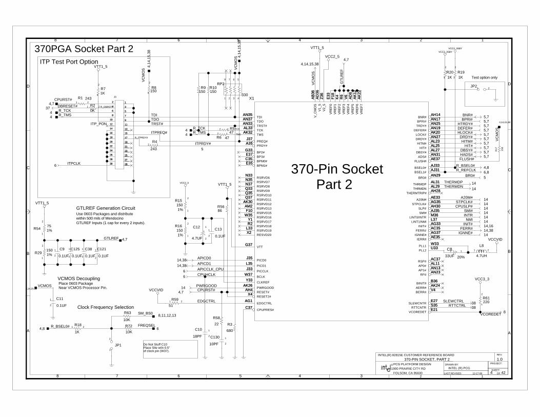
4
370-PIN SOCKET, PART 2
6,8R_REFCLK
4,7GTLREF
EDGCTRL
TDITDOTRST#
TCK
TMSITPREQ#
5ITPRDY#
4,14,15,38
VC
MO
S
4,7
GT
LRE
F
VCOREDET8
38RTTCTRLSLEWCTRL 38
14IGNNE#FERR# 14,38
14,16INIT#14NMI14INTR14SMI#14CPUSLP#14STPCLK#14A20M#
BR0# 5
FLUSH#5,7HADS#5,7DBSY#5,7HIT#5,7HITM#5,7DRDY#5,7HLOCK#5,7DEFER#5,7HTRDY#
APICD014,38APICD114,38APICCLK_CPU6
6 CPUHCLK
14 PWRGOODCPURST#4,7
5,7BPRI#5,7BNR#
C130
10PF 2
1
J3
4 R_TCKITP_PON
6 ITPCLK
37 DBRESET#0KR21 2
243R11 2
R71K1
2
R6 4712
4,7CPURST#
1501%R29
2
10.1UF
C1251
2
C8
20%33UF2 1
R_DBRST#
RP2
330
8 7 6 5
4321
4.7UH
L821
R8150
2
1
VC
MO
S
4,14
,15,
38
R61220
2
1
R191K
2
11KR20
1
2
4 R_TMS 47R512
R4
24312
R_ITPRDY#
150
R17
4,14,15,38
VC
MO
S
4,14,15,38VCMOS
751%R54
1
2
0.1UF
C1211
2
R10150
4 R_TCK
4 R_TMS
4,14
,15,
38V
CM
OS
0.1UF
C11
2
1
4.7UF
C12
2
1
0.1UF
C131
2
1%150
R152
1
R9150
4,8R_BSEL0#
R161501% 1
2
R59
5121
JP21 2
JP11
2
6FREQSEL
8,11,12,13SM_BS0
4,8R_BSEL0# R18
1K21
14THERMDP
14THERMDN
C9
0.1UF
1
2
C38
0.1UF
1
2
C10
18PF
1
2
R3
680
R58
22
R63
10K
R72
10K
X1
R5686
VCC3_3SBY
12 11
14 13
16 15
18 17
20 19
22 21
24 23
26 25
28 27
30 29
3
6 5
8 7
10
4
2 1
99
12
4
10
78
56
3
2930
2728
2526
2324
2122
1920
1718
1516
1314
1112
VCCVID
VTT1_5
VTT1_5
+
VCCVID
VCC2_5
VCC3_3
VCC2_5
+
VTT1_5
VTT1_5
VCC3_3SBY
A20M#AE33
ADS#AN31
AK24AERR#
AL11AP0#AP1#
AN13
W37BCLK
BERR#V4
B36BINIT#
AH14BNR#
G33BP2#
E37BP3#BPM0#
C35
BPM1#E35
BPRI#AN17
AN29BR0#
AJ33BSEL0#
AJ31BSEL1#
Y33CLKREF
C37CPUPRES#
DBSY#AL27
DEFER#AN19
DRDY#AN27
AG1EDGCTRL
AC35FERR#
AE37FLUSH#
HIT#AL25
HITM#AL23
AE35IERR#
AG37IGNNE#
AG33INIT#
LINT0/INTRM36
LINT1/NMIL37
LOCK#AK20
J33PICCLK
J35PICD0
L35PICD1
W33PLL1 U33PLL2
PRDY#A35 PREQ#J37
AK26PWRGOODRESET#
AH4X4
RESET2#
X2RESVD20
AN23RP#
RSP#AC37
RSRVD10Q35Q37
RSRVD11RSRVD12
AK30AM2
RSRVD13F10
RSRVD15RSRVD16
W35
RSRVD17Y1R2
RSRVD18L33RSRVD19
RSRVD6N33N35
RSRVD7RSRVD8
N37Q33
RSRVD9
VTTG37
S35RTTCNTR
E27SLEWCNTR
SLP#AH30
SMI#AJ35
STPCLK#AG35
TCKAL33
AN35TDITDO
AN37
THERMTRIP#AH28
THRMDNAL29AL31
THRMDP
TMSAK32
TRDY#AN25AN33
TRST#
V1_
5A
D36
V2_
5Z
36
VCOREDETE21
VR
EF
0E
33
VR
EF
1F
18
VR
EF
2K
4R
6V
RE
F3
VR
EF
4V
6
VR
EF
5A
D6
VR
EF
6A
K12
VR
EF
7A
K22
V_C
MO
SA
B36
X2
AB
36
AK
22A
K12
AD
6V
6R
6K
4F
18E
33
E21
Z36
AD
36
AN33 AN25
AK32
AL31AL29AH28
AN37AN35
AL33
AG35
AJ35AH30
E27S35
Q33N37N35N33
L33
G37
R2Y1
W35F10
AM2AK30Q37Q35
AC37
AN23
X4AH4
AK26
J37A35
U33W33
L35
J35
J33
AK20
L37M36
AG33
AG37AE35
AL23AL25
AE37
AC35
AG1
AN27
AN19
AL27
C37
Y33
AJ31AJ33
AN29
AN17
E35C35E37G33
AH14
B36
V4
W37
AN13AL11
AK24
AN31
AE33
B
C
D
8 7 6 5 4 3 2 1
D
C
B
A
345678
A
2 1OFFOLSOM, CA 95630
1900 PRAIRIE CITY RD
PROJECT:
REV:
DRAWN BY:
SHEET:LAST REVISED:
PCG PLATFORM DESIGNINTEL (R) PCG
42
1.0INTEL(R) 82815E CUSTOMER REFERENCE BOARD
R
12-17-99
ITP Test Port Option
Part 2370-Pin Socket
GTLREF Generation Circuit
within 500 mils of MendocinoUse 0603 Packages and distribute
GTLREF Inputs (1 cap for every 2 inputs).
370PGA Socket Part 2
Test option only
Near VCMOS Processor Pin.Place 0603 PackageVCMOS Decoupling
Clock Frequency Selection
Place Site w/in 0.5"of clock pin (W37).
Do Not Stuff C10

5
AGTL TERMINATION
4,7HTRDY#
3,7HREQ#3
4,7HADS#
BNR# 4,7
56
RP31
4,7HIT#
4,7DEFER#
BPRI# 4,7
ITPRDY# 4
RP33
56
RP24
56
56
RP32
56
RP23
RP22
56
56
RP21
56
RP1956
RP656
RP5
RP25
56RP28
56
56
RP26
56
RP27
RP17
56RP18
56
RP15
56
RP16
56
56
RP1456
RP11
RP13
56
RP9
56
RP12
56RP29
56
56
RP20
4BR0#
4,7DBSY#DRDY# 4,7
RP8
56
56
RP30
4,7HITM#
4,7HLOCK#
HREQ#03,7
3,7HREQ#1
HREQ#2 3,7
HREQ#4 3,7
RS#0 3,7
3,7RS#1 HD#40
HD#56HD#61HD#62HD#46
HD#60HD#50HD#53HD#58
HD#57HD#63HD#59HD#48
HD#47HD#27HD#44HD#45
HD#49HD#51HD#41HD#42
HD#36HD#22HD#43HD#34
HD#39HD#37HD#38HD#28
HD#52HD#55HD#54
HD#[63:0] 3,7HD#15
HD#33HD#35HD#19HD#29
HD#26HD#25HD#32HD#31
HD#2HD#14HD#18HD#13
HD#20HD#11HD#7HD#30
HD#17HD#10HD#12HD#3
HD#24HD#21
HD#16
HD#4HD#9HD#5HD#8
HD#1HD#0HD#6
HD#23RS#2 3,7
56
R21
150
R27
HA#29HA#26
HA#27
HA#25
HA#24
HA#23
HA#22
HA#21
HA#20
HA#19
HA#17
HA#16
HA#15
HA#11
HA#18
HA#14
HA#10
HA#13
HA#12HA#3
HA#30
HA#31
HA#4
HA#5
HA#6
HA#7
HA#8
HA#[31:3]
3,7
HA#28
HA#9
RP3
56
1
2
3
4 5
6
7
88
7
6
54
3
2
1
VTT1_5VTT1_5VTT1_5VTT1_5
1
2
3
4 5
6
7
88
7
6
54
3
2
1
1
2
3
4 5
6
7
88
7
6
54
3
2
1
1
2
3
4 5
6
7
88
7
6
54
3
2
1
1
2
3
4 5
6
7
88
7
6
54
3
2
1
1
2
3
4 5
6
7
88
7
6
54
3
2
1
1
2
3
4 5
6
7
88
7
6
54
3
2
1
1
2
3
4 5
6
7
88
7
6
54
3
2
1
1
2
3
4 5
6
7
88
7
6
54
3
2
1
1
2
3
4 5
6
7
88
7
6
54
3
2
1
1
2
3
4 5
6
7
88
7
6
54
3
2
1
1
2
3
4 5
6
7
88
7
6
54
3
2
1
1
2
3
4 5
6
7
88
7
6
54
3
2
1
1
2
3
4 5
6
7
88
7
6
54
3
2
1
1
2
3
4 5
6
7
88
7
6
54
3
2
1
1
2
3
4 5
6
7
88
7
6
54
3
2
1 1
2
3
4 5
6
7
88
7
6
54
3
2
1
1
2
3
4 5
6
7
88
7
6
54
3
2
1
1
2
3
4 5
6
7
88
7
6
54
3
2
1
1
2
3
4 5
6
7
88
7
6
54
3
2
1
1
2
3
4 5
6
7
88
7
6
54
3
2
1
1
2
3
4 5
6
7
88
7
6
54
3
2
1
1
2
3
4 5
6
7
88
7
6
54
3
2
1
1
2
3
4 5
6
7
88
7
6
54
3
2
1
1
2
3
4 5
6
7
88
7
6
54
3
2
1
1
2
3
4 5
6
7
88
7
6
54
3
2
1
1
2
3
4 5
6
7
88
7
6
54
3
2
1
B
C
D
8 7 6 5 4 3 2 1
D
C
B
A
345678
A
2 1OFFOLSOM, CA 95630
1900 PRAIRIE CITY RD
PROJECT:
REV:
DRAWN BY:
SHEET:LAST REVISED:
PCG PLATFORM DESIGNINTEL (R) PCG
42
1.0INTEL(R) 82815E CUSTOMER REFERENCE BOARD
R
12-17-99
1
2
3
4 5
6
7
81
2
3
4 5
6
7
8
AGTL Termination
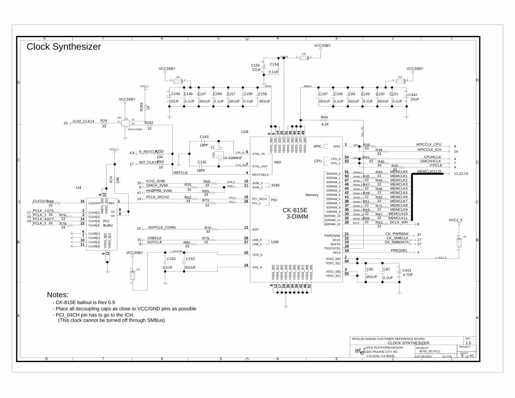
6
CLOCK SYNTHESIZER
U4
MEMV3PCIV3
33R98CLKOUT
19 PCLK_4PCLK_318
PCLK_117
L15
R6622
22R67
R6922
22R71DRAM_8
DRAM_9
DRAM_10
DRAM_11
APIC
4,8 R_REFCLK
3V66_1
XTAL_IN
XTAL_OUT
3V66_0
27CK_SMBDATA27CK_SMBCLK
CK_PWRDN# 37
DRAM_7
DRAM_6
DRAM_5
DRAM_2
DRAM_1
DRAM_0
DOTCLK9
USBCLK15
0.1UF
C108
.001UF
C107
L11
C150
.001UF
C151
0.1UF
R44
8.2K
R7633
4ITPCLK7GMCHHCLK4CPUHCLK
14APICCLK_ICH4APICCLK_CPU
15 ICH2_3V66
8DCLK_WR
14 PCLK_0/ICH2
14.318MHZ
Y1
0.1UF
C154
.001UF
C84
C15522UF
18PF
C143
0.1UF
C146
C152
0.1UF
C147
.001UF
.001UF
C153
22UFC442
0.1UF
C87
4.7UFC443
L16
R4322R45
2222
R46
22R47
22R48
R4922
22R50
R5122
ICH2_CLK1415
R64
10
22UF
C144
L37
R3933
R4133 R40
33
33R38
R5222
C156
0.1UF
C157
.001UF
C158
0.1UF
C159
.001UF 0.1UF
C149
SIO_CLK1417
10R79
18PF
C14510K
R255
R6833
R6233 PCI_1
PCI_0
33R73
9 GMCH_3V66 R2533
33R80
U10
10 AGPCLK_CONN33
R70
10
R292R24
33
41 HUBPRB_3V66
33R42
CPU_0_1
MEMCLK11MEMCLK10MEMCLK9
MEMCLK0MEMCLK1MEMCLK2MEMCLK3MEMCLK4MEMCLK5MEMCLK6MEMCLK7
11,12,13MEMCLK[11:0]
MEMCLK8
4FREQSEL
DCLK
SE
L1_P
U
33R65
33R78
1KR29
3
10K
R74
33R7733
R75
L_VCC2_5
USBV3
PCLK_5
L_CKVDDA
DRAM_4
DRAM_3
U18
REFCLK
L14
C85
.001UF
CLKA[1]2
CLKA[2]3
CLKA[3]14
CLKA[4]15
CLKB[1]6
CLKB[2]7
CLKB[3]10
CLKB[4]11
1REF
S289
S1
5V
SS
3_3[
0]V
SS
3_3[
1]12
VD
D3_
3[0]
4 13V
DD
3_3[
1]16CLKOUT
PCIBuffer
16
134
125
98
1
111076
151432
12
VCC3SBY
1 2
XT
AL
21
+2
1
+1
2
+2
1
1 2
+1
2
VCC2_5
12
VCC3SBY VCC3SBY
VCC3SBY
SN74LVC08A
111214
13
7
VCC3SBY
B
C
D
8 7 6 5 4 3 2 1
D
C
B
A
345678
A
2 1OFFOLSOM, CA 95630
1900 PRAIRIE CITY RD
PROJECT:
REV:
DRAWN BY:
SHEET:LAST REVISED:
PCG PLATFORM DESIGNINTEL (R) PCG
42
1.0INTEL(R) 82815E CUSTOMER REFERENCE BOARD
R
12-17-99
VCC3_3
VCC3_3
VD
D3_
3[8]
49
29SDRAM_12
103V66_03V66_1
11
APIC1
CPU_05453
CPU_1
PWRDWN#21
REF/FSEL14
22SCLK
51SDRAM_0SDRAM_1
5047
SDRAM_2SDRAM_3
4645
SDRAM_4SDRAM_5
4241
SDRAM_6SDRAM_7
38
18SEL0
USB_026
USB_127
VDD2_5[0]2
VDD2_5[1]56
VD
D3_
3[2]
14
VDD_A20
55VSS2_5[1]
3VSS2_5[0]
8V
SS
3_3[
0]V
SS
3_3[
1]13 17
VS
S3_
3[2]
34V
SS
3_3[
5]VSS_A19
6XTAL_IN
XTAL_OUT7
AGP12
15PCI_0/ICHPCI_1
16
VD
D3_
3[0]
5 9V
DD
3_3[
1]
28TRISTATE#
SDATA23
37SDRAM_8SDRAM_9
3633
SDRAM_1032
SDRAM_11
25V
DD
3_3[
3]
35V
DD
3_3[
5]V
DD
3_3[
4]31 40
VD
D3_
3[6]
VD
D3_
3[7]
44
VS
S3_
3[3]
24
VS
S3_
3[4]
30
VS
S3_
3[9]
5248V
SS
3_3[
8]V
SS
3_3[
7]43
VS
S3_
3[6]
39
CPU
APIC
USB
REF
3V66
CK-815E3-DIMM
PCIMemory
39 43 48 523024
444031 3525
32333637
2328
95
1615
12
7
6
19
3417138355
20
14
562
2726
18
3841424546475051
22
4
21
5354
1
1110
29
49
1 2
- PCI_0/ICH pin has to go to the ICH.(This clock cannot be turned off through SMBus)
Notes:
Clock Synthesizer
- Place all decoupling caps as close to VCC/GND pins as possible- CK-815E ballout is Rev 0.9

7
10,14,16,17,18,19,20,26PCIRST#
HLOCK#4,54,5 DEFER#
HADS#4,54,5 BNR#
BPRI#4,54,5 DBSY#
4,5 DRDY#
4,5 HITM#
4,5 HTRDY#
3,5HA#[31:3]
HA#3HA#4HA#5HA#6HA#7HA#8HA#9HA#10HA#11HA#12HA#13HA#14HA#15HA#16HA#17HA#18HA#19HA#20HA#21HA#22HA#23HA#24HA#25HA#26HA#27HA#28HA#29HA#30HA#31
3HREQ#[4:0] HREQ#0
HREQ#1HREQ#2HREQ#3HREQ#4
3RS#[2:0]
RS#0RS#1RS#2
3,5HD#[63:0]
HD#63HD#62HD#61HD#60HD#59HD#58HD#57HD#56HD#55HD#54HD#53HD#52HD#51HD#50HD#49HD#48HD#47HD#46HD#45HD#44HD#43HD#42HD#41HD#40HD#39HD#38HD#37HD#36HD#35HD#34HD#33HD#32HD#31HD#30HD#29HD#28HD#27HD#26HD#25HD#24HD#23HD#22HD#21HD#20HD#19HD#18HD#17HD#16HD#15HD#14HD#13HD#12HD#11HD#10HD#9HD#8HD#7HD#6HD#5HD#4HD#3HD#2HD#1HD#0
0.1UF
C123 C124
0.1UF
4,5 HIT#
18PF
C90
6 GMCHHCLK
CPURST#4
4GTLREF
86R55
U21
GMCH: HOST INTERFACE
VTT1_5
B
C
D
8 7 6 5 4 3 2 1
D
C
B
A
345678
A
2 1OFFOLSOM, CA 95630
1900 PRAIRIE CITY RD
PROJECT:
REV:
DRAWN BY:
SHEET:LAST REVISED:
PCG PLATFORM DESIGNINTEL (R) PCG
42
1.0INTEL(R) 82815E CUSTOMER REFERENCE BOARD
R
12-17-99
GN
D;P
11,P
12,P
13,P
14,P
15,P
16,R
2,R
6,R
11,R
12,R
13,R
14,R
15,R
16,R
23,R
25,T
4,T
11,T
12,T
13,T
14,T
15,T
16
GN
D;A
E2,
AE
4,A
E6,
AE
8,A
E10
,AE
12,A
E14
,AE
16,A
E18
,AE
20
VC
C1_
8;W
6,Y
9,Y
18,A
A6,
AA
8,A
A11
,AA
13,A
A15
,AA
17,A
A19
,AB
16,A
B20
,AC
22,A
D19
GN
D;A
B4,
E7,
AC
2,A
C5,
AC
7,A
C9,
AC
11,A
C13
,AC
15,A
C17
,AC
19,A
C21
,AC
25
GN
D;L
15,L
16,L
22,L
25,M
4,M
11,M
12,M
13,M
14,M
15,M
16,N
2,N
6,N
11,N
12,N
13,N
14,N
15,N
16,N
23,P
4,A
A23
GN
D;F
16,F
25,G
9,G
17,G
21,G
23,P
24,H
6,H
22,J
2,J5
,J23
,J25
,K4,
K7,
K21
,L2,
L6,L
11,L
12,L
13,L
14,A
A25
GN
D;T
21,U
2,U
7,K
24,V
4,V
6,V
20,V
22,W
2,W
7,W
23,W
25,Y
4,Y
6,Y
8,Y
10,Y
17,Y
19,A
A2,
AA
9,A
A12
,AA
14,A
A16
GN
D;B
26,C
3,C
6,C
9,C
12,C
15,C
18,C
21,C
24,D
1,E
5,E
10,E
12,E
15,E
17,E
20,F
1,F
3,F
11,F
13
VC
C1_
8;C
25,E
24,F
23,G
22,J
7,K
6,M
6,P
6,T
6,V
7,G
26,Y
7
VC
C1_
8;A
A21
,E23
,AF
26,A
F25
GN
D;A
F24
,AE
25,E
22
VC
C3_
3SB
Y;B
2,B
5,B
8,B
11,B
14,B
19,B
22,B
25,E
2,F
10,F
14,F
17,G
6,G
8,G
19,H
2,H
5,H
7
VD
DQ
;K20
,Y24
,L21
,M23
,U25
,N25
,R21
,U20
,U23
,W20
G1 ADS#N4 BNR#M5 BPRI#
AA5CPURST#
J3DBSY#
M3DEFER#
J1DRDY#
U6GTLREFA
AA10GTLREFB
U1HA10#
P2HA11#
T1HA12#
T3HA13#
P3HA14#
T5HA15#
R5HA16#
V5 HA17#Y2 HA18#V3
HA19#W1
HA20#U4
HA21#V2
HA22#W3
HA23#W4
HA24#U5
HA25#Y5
HA26#Y3
HA27#U3 HA28#Y1 HA29#
R4HA3#
W5HA30#
V1HA31#
P1HA4#
T2 HA5#R3 HA6#N5 HA7#P5
HA8#R1
HA9#
AA7HCLK
AA1HD0#
AB2HD1#
AD1HD10#
AE3HD11#
AD2HD12#
AD3HD13#
AF1HD14#
AA4HD15#
AD6HD16#
AC3HD17#AE1HD18#AB6HD19#
AF2HD2#
AF4HD20#
AE5HD21#
AC8HD22#
AB5HD23#
AF5HD24#
AC6HD25#
AF6HD26#
AD11HD27#
AF8HD28#AD8HD29#
AD4HD3#
AD5HD30#AB7
HD31#AF7
HD32#AD7
HD33#AB8
HD34#AE7
HD35#AE9
HD36#AB9
HD37#AF9
HD38#AD10
HD39#
AB1HD4#
AF12HD40#AB11HD41#AB10
HD42#AD9
HD43#AC10
HD44#AF10
HD45#AD14
HD46#AD12
HD47#AB12
HD48#AE11
HD49#
AB3HD5#
AE15HD50#
AF11HD51#AF13HD52#AB14
HD53#AF14
HD54#AB13
HD55#AB15
HD56#AE13
HD57#AC14
HD58#AD13
HD59#
AA3HD6#
AD15HD60#
AF16HD61#
AF15HD62#AC12HD63#
AC4HD7#AC1HD8#AF3
HD9#
HIT#K1
HITM#L3
L4HLOCK#
M1HREQ0#
N1HREQ1#
M2HREQ2#
L5HREQ3#
N3HREQ4#
HTRDY#K3
H3RESET#
K2 RS0#L1 RS1#H1
RS2#H1L1K2
H3
K3
N3L5M2N1M1
L4
L3K1
AF3AC1AC4
AC12AF15AF16AD15
AA3
AD13AC14AE13AB15AB13AF14AB14AF13AF11AE15
AB3
AE11AB12AD12AD14AF10AC10AD9AB10AB11AF12
AB1
AD10AF9AB9AE9AE7AB8AD7AF7AB7AD5
AD4
AD8AF8AD11AF6AC6AF5AB5AC8AE5AF4
AF2
AB6AE1AC3AD6AA4AF1AD3AD2AE3AD1
AB2AA1
AA7
R1P5N5R3T2P1
V1W5
R4
Y1U3Y3Y5U5W4W3V2U4W1V3Y2V5R5T5P3T3T1P2U1
AA10U6
J1
M3
J3
AA5
M5N4G1
Place C123, C124 close to GMCH
GMCH, Part 1; Host Interface, Power and GND

8
SM_CKE5SM_CKE4
SM_CKE[5:0]11,12,13 SM_CKE0
SM_CKE1SM_CKE2SM_CKE3
SM_CSB#4SM_CSB#5
SM_CSB#3
SM_CSB#1SM_CSB#011,12,13
SM_CSB#[5:0]
SM_CSB#2
SM_MAC5#SM_MAC6#SM_MAC7#
13SM_MAC[7:4]#
SM_MAC4#
SM_MAB7#
12SM_MAB[7:4]#
SM_MAB6#SM_MAB5#SM_MAB4#
SM_BS0SM_BS1
SM_BS[1:0]11,12,13
SM_CSA#2SM_CSA#1SM_CSA#0SM_CSA#[5:0]
11,12,13
SM_CSA#3
SM_CSA#5SM_CSA#4
8,11,12,13 SM_RAS#
8,11,12,13 SM_CAS#
8,11,12,13 SM_WE#
6DCLK_WR
SM_MD1SM_MD2SM_MD3SM_MD4SM_MD5SM_MD6SM_MD7SM_MD8SM_MD9SM_MD10
SM_MD12SM_MD13SM_MD14SM_MD15SM_MD16SM_MD17SM_MD18SM_MD19SM_MD20SM_MD21
SM_MD23SM_MD24SM_MD25SM_MD26SM_MD27
SM_MD29SM_MD30SM_MD31SM_MD32SM_MD33SM_MD34
SM_MD36SM_MD37SM_MD38SM_MD39SM_MD40SM_MD41SM_MD42SM_MD43SM_MD44SM_MD45SM_MD46SM_MD47SM_MD48SM_MD49SM_MD50SM_MD51SM_MD52SM_MD53SM_MD54SM_MD55SM_MD56SM_MD57SM_MD58SM_MD59SM_MD60SM_MD61SM_MD62SM_MD63
SM_MD0
SM_MD28
SM_MD35
11,12,13SM_MD[63:0]
SM_MD11
SM_MD22
SM_DQM[7:0]11,12,13 SM_DQM0
SM_DQM1SM_DQM2SM_DQM3SM_DQM4SM_DQM5SM_DQM6SM_DQM7
8,11,12,13SM_MAA12
8,11,12,13SM_MAA10JP11
JP7 SM_BS0 4,8,11,12,13
JP12 SM_RAS# 8,11,12,13
1%301R166
R1673011%
8,11,12,13SM_BS1
JP10
10K
RP36
10K
RP35
JP8
4,6 R_REFCLK
JP9 SM_MAA118,11,12,13
4VCOREDET
10K
RP37
RP43
10
SM_MAA6SM_MAA5SM_MAA4
SM_MAA12SM_MAA11
SM_MAA8
SM_MAA10SM_MAA9
SM_MAA2
SM_MAA011,12,13
SM_MAA[12:0]
SM_MAA1
SM_MAA3
SM_MAA7
4 R_BSEL0#
8,11,12,13SM_WE#
8,11,12,13SM_MAA9
SM_CAS# 8,11,12,13
1%40
R60
22PFC140
9,14,41HUBREF
C920.1UF
10
RP44
10
RP4
U21
GMCH: SYSTEM MEMORY
VCC1_8
1 2 3 456788 7 6 5
43211 2 3 45678
1 2 3 45678
1 2 3 45678
1 2 3 45678
1
2
3
45
6
7
88
7
6
5 4
3
2
1
VCC3SBY
B
C
D
8 7 6 5 4 3 2 1
D
C
B
A
345678
A
2 1OFFOLSOM, CA 95630
1900 PRAIRIE CITY RD
PROJECT:
REV:
DRAWN BY:
SHEET:LAST REVISED:
PCG PLATFORM DESIGNINTEL (R) PCG
42
1.0INTEL(R) 82815E CUSTOMER REFERENCE BOARD
R
12-17-99
1
2
3
45
6
7
8 1
2
3
45
6
7
8
1
2
3
45
6
7
88
7
6
5 4
3
2
1
SDQM1F15
SDQM2A7A6
SDQM3A18
SDQM4
SCKE2E9
B9SCSB4#
SCSB0#F9
SCSB1#F8
D10 SCSB2#D9 SCSB3#
E13 SCSA4#
B13 SBS0
D18 SCAS#
SCKE0D8
SCKE1E8
SCSA0#D15
SCSA1#A17D14 SCSA2#E14 SCSA3#
E11SMAA10SMAA11
A13
D12SMAA8
C13SMAA9
SMAB5#A15
SMAB6#C14
SMAB7#A14
D19SMD10
E18SMD11B18SMD12F18SMD13
D17SMD15
A3SMD16
A1SMD17
C1SMD18
F2SMD19
G3SMD20
B4SMD23D4SMD24
D3SMD26
F5SMD28
G4SMD29
F21SMD3
J6SMD30
A25SMD33
B24SMD34A24SMD35B23
SMD36A23
SMD37C22
SMD38A22
SMD39
E21SMD4
D21SMD40
B21SMD41
A21SMD42
C20SMD43
B20SMD44
A20SMD45C19SMD46A19
SMD47A4
SMD48A2
SMD49
G20SMD5
B1SMD50
E1SMD51
G2SMD52
E6SMD53
D5SMD54
C4SMD55SMD56 B3
SMD57 D2
SMD58E3F4
SMD59
F20SMD6
F6SMD60
G5SMD61
D20SMD7
F19SMD8
E19SMD9
C16SRAS#
E16 SWE#
K5SMD31
D22SMD2
C23SMD1
H4SMD62
C8 SCKE4C7
SCKE5
SMD63J4
SCLKF7
SCKE3D7
SDQM7A5
E4SMD27
C17SDQM5
SMAC5#A10
SMAC6#C10
SMAC7#A9
SMAC4#B10
B16SMAA1
F12SMAA2
A16SMAA3
SMAA12B7
SMAB4#B15
B17SCSA5#
SDQM0D16
A26SMD32
D23SMD0D13SMAA0
D11 SBS1
A8SCSB5#
B6SDQM6
G18SMD14
C5SMD22
D6SMD21
C2SMD25
A11 SMAA7
B12SMAA4
A12 SMAA5C11 SMAA6
G10 RESVD
G7SRCOMP
G10
C11A12B12
A11
C2
D6C5
G18
B6
A8
D11
G7
D13D23
A26
D16
B17
B15
B7
A16F12B16
B10
A9C10A10
C17
E4
A5
D7
F7
J4
C7C8
H4
C23D22
K5
E16
C16
E19F19D20
G5F6
F20
F4E3D2B3C4D5E6G2E1B1
G20
A2A4A19C19A20B20C20A21B21D21
E21
A22C22A23B23A24B24A25
J6
F21
G4F5
D3
D4B4
G3F2C1A1A3D17
F18B18E18D19
A14C14A15
C13D12
A13E11
E14D14A17D15
E8D8
D18
B13
E13
D9D10
F8F9
B9
E9
A18A6A7
F15
Reserved Strap
Place HUBREF GenerationCircuit in middle ofGMCH and ICH.
GMCH RESET STRAPS
Host Freq; high = 100, low = 66
FSB P-MOS kicker; high = NON-Cu, low = Cu
Host Freq; high = 133, low = 100/66
SM /LM muxing strap, active low
IOQ depth; high = 4; low = 1
ALLZ; high = Normal, low = ALLZ
XOR chain; high = Normal, low = XOR
Reserved Strap
GMCH, Part 2; Memory Interface

9
273VDDCDA3VDDCCL 27
26,273VFTSDA
26,273VFTSCL
0.1UFC190
14,41HLSTB#HLSTB 14,41
8,14,41HUBREF
HL6HL5
HL10HL9
HL0HL1HL2HL3HL4
HL8HL7
14,41HL[10:0]
6GMCH_3V6627VID_BLUE27VID_GREEN27VID_RED27CRT_HSYNC
CRT_VSYNC 27
IREFPD
FTVSYNC 2626FTCLK1
FTCLK0 26
SL_STALL26FTBLNK#
FTD4FTD5FTD6FTD7FTD8FTD9
FTD10FTD11
FTD0FTD1FTD2FTD3
26FTD[11:0]
GCBE#3GCBE#2GCBE#1GCBE#0
10GCBE#[3:0]
10 GFRAME#
10GDEVSEL#
10GIRDY#
10GTRDY#
10GSTOP#
10GPAR
10 GREQ#
10 GGNT#
10 PIPE#
10ADSTB0
10ADSTB0#
10 ADSTB1
10 ADSTB1#
10 SBSTB
10 SBSTB#ST0
10ST[2:0]
ST1ST2
10RBF#
10WBF#
1%174
R86
C279
500PF
10 GMCH_AGPREF
18PFC196
SBA4
SBA1SBA2SBA3
SBA5SBA6
SBA0 10SBA[7:0]
SBA7
0.01UF
C239
1%
R11640
1%
R10340
GAD31
10GAD[31:0]
GAD2GAD3GAD4GAD5GAD6GAD7GAD8GAD9GAD10GAD11GAD12GAD13GAD14GAD15GAD16GAD17GAD18GAD19GAD20
GAD22
GAD24GAD25GAD26GAD27GAD28GAD29GAD30
GAD0GAD1
GAD23
GAD21
10R101
1%
R1691K
1%
R1701K
C280
500PF
1%
R16882
1%
R17182
6DOTCLK
CONN_AGPREF10
RCLKOCLK
26FTHSYNC
22PFC233
U21
GMCH: DISPLAY CACHE, VIDEO, AND HUB INTERFACE
21
VDDQ
VCC1_8
1 2
B
C
D
8 7 6 5 4 3 2 1
D
C
B
A
345678
A
2 1OFFOLSOM, CA 95630
1900 PRAIRIE CITY RD
PROJECT:
REV:
DRAWN BY:
SHEET:LAST REVISED:
PCG PLATFORM DESIGNINTEL (R) PCG
42
1.0INTEL(R) 82815E CUSTOMER REFERENCE BOARD
R
12-17-99
ADSTB0M22
ADSTB0#L23
ADSTB1U22V23
ADSTB1#
AGPREFJ24
AB19BLANK#
AE23BLUE
CLKOUT0 AE19
CLKOUT1 AF19
AE24DCLKREF
LTVCL AB21
K26GAD0/LDQM0
J22GAD1/LMD4
M24GAD10/LDQM1
M26GAD11/LMA2
M21GAD12/LMD8
N24 GAD13/LMA5N22 GAD14/LMD9N26 GAD15/LMA1T26
GAD16/LMA8T22
GAD17/LMD14U24
GAD18/LMA11T23
GAD19/LMD15
K25 GAD2/LMD7
U26GAD20/LMA9
T24GAD21/LMD16
V24GAD22/LMA0
U21GAD23/LMD17
V25 GAD24/LCKEV21 GAD25/LMD18V26 GAD26/LCAS#W21
GAD27/LMD19W24
GAD28/LTCLK1W22
GAD29/LMD20
J21 GAD3/LMD3
W26GAD30/LTCLK0
Y21GAD31/LMD21
L24 GAD4/LMD6J20
GAD5/LMD2L26
GAD6/LMD5K23
GAD7/LMD1K22
GAD8/LMD0M25
GAD9/LMA4
H23GCBE0#/LMA3
N21GCBE1#/LMD10
T25GCBE2#/LMD13
Y26GCBE3#/LRAS#
P26GDEVSEL#/LMD11
R26 GFRAME#/LMA10
AD25GGNT#
P23GIRDY#/LMD12
R24GPAR/LMA6
GRCOMPJ26
AE22GREEN
AE26GREQ#/LMD27
P25GSTOP#/LCS#
P21GTRDY#/LMA7
HCOMP H20
H24HL0H26HL1
HL10 C26
H25HL2G24HL3F24HL4E26HL5E25HL6
HL7 D26
HL8 D25
HL9 D24
F22HLCLK
HLSTB G25
HLSTB# F26
AF23HSYNC
HUBREF H21
AD23IREF
IWASTE Y20
DDCCKAB18
AD16LTVDATA0
AF17LTVDATA1
AE21LTVDATA10
AD21LTVDATA11
AE17LTVDATA2AD17LTVDATA3AF18LTVDATA4AD18
LTVDATA5AF20
LTVDATA6AD20
LTVDATA7AC20
LTVDATA8LTVDATA9
AF21
OCLOCKR22
AC26PIPE#/LMD24
RBF#/LMD30AD26
RCLOCKP22
AD22RED
AB22SBA0/LMD31AB25SBA1/LMD25AB23SBA2/LDQM2AB26SBA3/LMD26AA22SBA4/LMD23AA26SBA5/LWE#Y22SBA6/LMD22Y25SBA7/LGM_FREQ_SEL
SBSTBY23
SBSTB#AA24
AD24ST0/LMD28ST1/LDQM3
AC24AC23
ST2/LMD29
AC18TVCLKIN/SL_STALL
TVHSYNCAB17
TVVSYNCAC16
AF22VSYNC
WBF#AB24
LTVDA AA20
AA18DDCDA AA18
AA20
AB24
AF22
AC16AB17
AC18
AC23AC24AD24
AA24Y23
Y25Y22AA26AA22AB26AB23AB25AB22
AD22
P22
AD26
AC26
R22
AF21AC20AD20AF20AD18AF18AD17
AE17
AD21AE21
AF17AD16
AB18
Y20AD23
H21
AF23
F26G25
F22
D24D25D26E25E26F24G24H25
C26
H26H24
H20
P21P25
AE26
AE22
J26
R24
P23
AD25
R26P26
Y26T25N21H23
M25K22K23L26J20L24
Y21W26
J21
W22W24W21V26V21V25U21V24T24U26
K25
T23U24T22T26N26N22N24M21M26M24
J22K26
AB21
AE24
AF19AE19
AE23
AB19
J24
V23U22L23M22
as possible to GMCH
Place Site w/in 0.5"of clock ball (AA21).
Place as close asPossible to GMCHand via straight toVSS plane.
Place R116 within 0.5" of the GMCH Ball. Do Not Stuff C196
Place Resistor as Close
NPO
GMCH, Part 3; AGP/Display Cache, and Video Interface
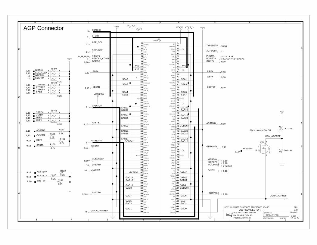
10
AGP CONNECTOR
RP49
8.2K9,10 GPAR9,10 GSTOP#9,10 GTRDY#9,10 GFRAME#
GSERR#10GPERR#10GDEVSEL#9,10GIRDY#9,10
GREQ#9,10GGNT#9,10PIPE#9,10WBF#9,10
9,10ADSTB1#
9,10ADSTB0#
9,10GPAR
14,18,19PCI_PME#
7,14,16,17,18,19,20,26PCIRST#14,18,19,38PIRQ#A
10,34TYPEDET#
J14
9,10GFRAME#
9,10ADSTB1#
9,10SBSTB#
9,10WBF#
9,10GDEVSEL#
9 GMCH_AGPREF
10,34TYPEDET#
200-1%
R57
301-1%
R11
4
CON_AGPREF
21AGPUSBN
8.2K
R1059,10 ADSTB1
9,10 ADSTB0
9,10 ADSTB0#
21AGP_OC#
9,10 GREQ#6 AGPCLK_CONN
14,18,19,38 PIRQ#B
21AGPUSBP
9,10 SBSTB
9,10RBF#
9,10GIRDY#
9,10ADSTB1
10 GPERR#
GCBE#0
GCBE#3
9GCBE#[3:0] GCBE#2
GCBE#110 GSERR#
9,10ADSTB0
9,10GGNT#
9,10PIPE#
9ST[2:0]
ST2ST0 ST1
9 SBA[7:0]
SBA7
SBA3
SBA1SBA0
SBA2
SBA4SBA6
SBA5
GAD20
GAD16
GAD30
GAD14
GAD2GAD4
GAD6
GAD9
GAD11GAD13
GAD15
GAD22
GAD24GAD26
GAD28
GAD18
GAD0GAD1
GAD3
GAD7
GAD8GAD10
GAD12
GAD19
GAD23
GAD25
GAD21
GAD17
GAD31GAD29
GAD27
9 GAD[31:0]
GAD5
9,10GSTOP# 9,10GTRDY#
Q10
RP50
8.2K
RP48
8.2K
8.2K
R163
9
CONN_AGPREF
R117
8.2K
R122
8.2K
9,10 SBSTB#8.2K
R159
8.2K
R154
R160
8.2K
9,10 RBF#
9,10 SBSTB
1
2
3
4 5
6
7
88
7
6
54
3
2
1
VDDQ
AGP4XU_20
B1OVRCNT#
5V_AB2
5V_BB3
B4USB+
GND_KB5
B6INTB#
CLKB7
B8REQ#
VCC3_3_FB9
B10ST0
ST2B11
B12RBF#
B13GND_L
SBA0B15
SBA2B17
B18SB_STB
GND_MB19
B20SBA4
A112V
TYPEDET#A2
A3RESV_A
USB-A4
A5GND_A
INTA#A6
RST#A7
A8GNT#
VCC3_3_AA9
ST1A10
A11RESV_B
B14RESV_H
PIPE#A12
A13GND_B
WBF#A14
A15SBA1
VCC3_3_BA16
A17SBA3
SB_STB#A18
A19GND_C
SBA5A20
SBA7A21B21
SBA6
A22RESV_C
GND_DA23
RESVB22
B23GND_N
A24RESV_D
A25VCC3_3_CVCC3_3_H
B25
B16VCC3_3_G
B26AD31
AD29B27
B28VCC3_3_I
B29AD27
B30AD25
GND_OB31
B32AD_STB1
AD23B33
AD30A26
A27AD28
VCC3_3_DA28
A29AD26
AD24A30
A31GND_E
AD_STB1#A32
A33C/BE3#
VDDQ_AA34B34
VDDQ_F
AD21B35
B36AD19
GND_PB37
B38AD17
C/BE2#B39
B40VDDQ_G VDDQ_B
A40
A39AD16
AD18A38
A37GND_F
AD20A36
A35AD22
B41IRDY#
GND_QB43
B44RESV_K
VCC3_3_JB45
B46DEVSEL#
VDDQ_HB47
A41FRAME#
RESV_EA42
A43GND_G
RESV_FA44
A45VCC3_3_E
TRDY#A46
A47STOP#
PME#A48
A49GND_H
B48PERR#
GND_RB49
PARA50
AD15A51
VDDQ_CA52
A53AD13
AD11A54
A55GND_I
AD9A56
A57C/BE0#
VDDQ_DA58
A59AD_STB0#
AD6A60
A61GND_J
A62AD4
A63AD2
A64VDDQ_E
A65AD0
SERR#B50
B51C/BE1#
VDDQ_IB52
B53AD14
B54AD12
GND_SB55
B56AD10
AD8B57
B58VDDQ_J
AD_STB0B59
B60AD7
GND_TB61
AD5B62
AD3B63
VDDQ_KB64
AD1B65
VREF_CGB66 A66
VREF_GC
3_3VAUX1B24
B423_3VAUX2
B42
B24
A66B66
B65
B64
B63
B62
B61
B60
B59
B58
B57
B56
B55
B54
B53
B52
B51
B50
A65
A64
A63
A62
A61
A60
A59
A58
A57
A56
A55
A54
A53
A52
A51
A50
B49
B48
A49
A48
A47
A46
A45
A44
A43
A42
A41
B47
B46
B45
B44
B43
B41
A35
A36
A37
A38
A39
A40B40
B39
B38
B37
B36
B35
B34 A34
A33
A32
A31
A30
A29
A28
A27
A26
B33
B32
B31
B30
B29
B28
B27
B26
B16
B25 A25
A24
B23
B22
A23
A22
B21 A21
A20
A19
A18
A17
A16
A15
A14
A13
A12
B14
A11
A10
A9
A8
A7
A6
A5
A4
A3
A2
A1
B20
B19
B18
B17
B15
B13
B12
B11
B10
B9
B8
B7
B6
B5
B4
B3
B2
B1
VCC12 VCC3_3VCC5 VDDQ
VCC3_3
VDDQ
VCC3SBY
VDDQ
2N70
02LT
1
G 1
D
3
S
2
S
D
G
1
2
3
4 5
6
7
88
7
6
54
3
2
1
1
2
3
4 5
6
7
81
2
3
4 5
6
7
8
B
C
D
8 7 6 5 4 3 2 1
D
C
B
A
345678
A
2 1OFFOLSOM, CA 95630
1900 PRAIRIE CITY RD
PROJECT:
REV:
DRAWN BY:
SHEET:LAST REVISED:
PCG PLATFORM DESIGNINTEL (R) PCG
42
1.0INTEL(R) 82815E CUSTOMER REFERENCE BOARD
R
12-17-99
AGP Connector
Place close to GMCH
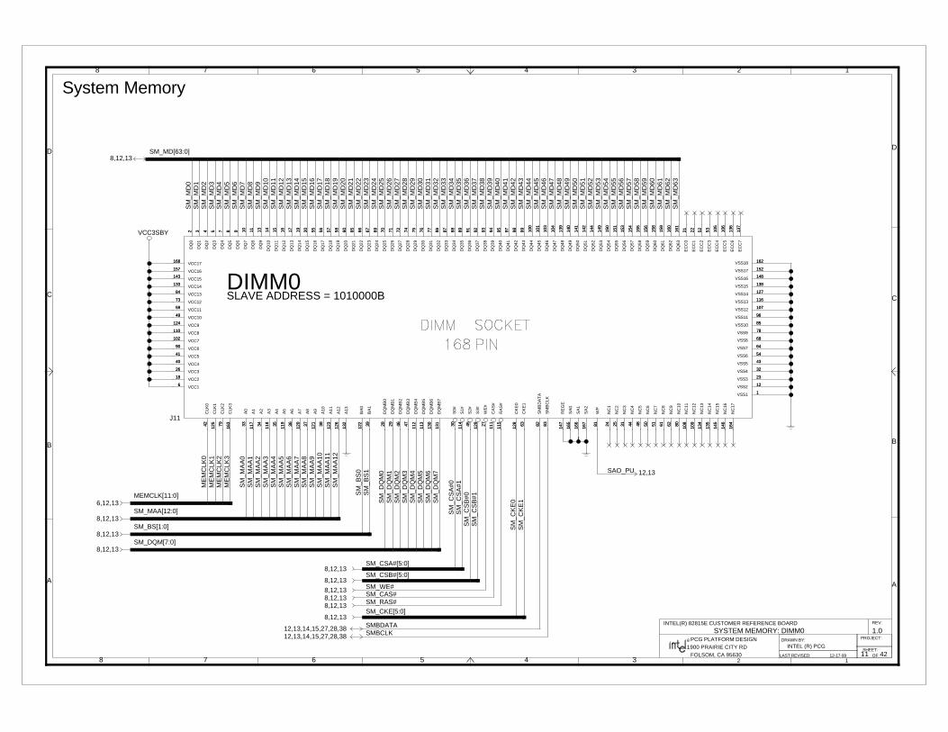
SLAVE ADDRESS = 1010000BDIMM0
11
SYSTEM MEMORY: DIMM0
SM_MD[63:0]8,12,13
SM
_MD
1
SM
_MD
10
SM
_MD
27
SM
_MD
61
SM
_MD
63S
M_M
D62
SM
_MD
60S
M_M
D59
SM
_MD
58S
M_M
D57
SM
_MD
56S
M_M
D55
SM
_MD
54S
M_M
D53
SM
_MD
52S
M_M
D51
SM
_MD
50S
M_M
D49
SM
_MD
48S
M_M
D47
SM
_MD
46S
M_M
D45
SM
_MD
44S
M_M
D43
SM
_MD
42S
M_M
D41
SM
_MD
40S
M_M
D39
SM
_MD
38S
M_M
D37
SM
_MD
36S
M_M
D35
SM
_MD
34S
M_M
D33
SM
_MD
32S
M_M
D31
SM
_MD
30S
M_M
D29
SM
_MD
28
SM
_MD
26S
M_M
D25
SM
_MD
24S
M_M
D23
SM
_MD
22S
M_M
D21
SM
_MD
20S
M_M
D19
SM
_MD
18S
M_M
D17
SM
_MD
16S
M_M
D15
SM
_MD
14S
M_M
D13
SM
_MD
12S
M_M
D11
SM
_MD
9S
M_M
D8
SM
_MD
7S
M_M
D6
SM
_MD
5S
M_M
D4
SM
_MD
3S
M_M
D2
SM
_MD
0
8,12,13 SM_RAS#8,12,13 SM_CAS#8,12,13 SM_WE#
6,12,13MEMCLK[11:0]
ME
MC
LK3
ME
MC
LK2
ME
MC
LK0
ME
MC
LK1
SMBCLK12,13,14,15,27,28,38
SMBDATA12,13,14,15,27,28,38
J11
12,13SAO_PU
8,12,13SM_DQM[7:0]
SM
_DQ
M2
SM
_DQ
M4
SM
_DQ
M5
SM
_DQ
M7
SM
_DQ
M3
SM
_DQ
M1
SM
_DQ
M0
SM
_DQ
M6
8,12,13SM_BS[1:0]
SM
_BS
1S
M_B
S0
SM_MAA[12:0]8,12,13
SM
_MA
A11
SM
_MA
A1
SM
_MA
A3
SM
_MA
A4
SM
_MA
A6
SM
_MA
A7
SM
_MA
A8
SM
_MA
A9
SM
_MA
A10
SM
_MA
A5
SM
_MA
A2
SM
_MA
A0
SM
_MA
A12
SM
_CK
E0
SM
_CK
E1
SM_CKE[5:0]8,12,13
SM
_CS
A#0
SM
_CS
A#1
8,12,13SM_CSA#[5:0]
SM
_CS
B#1
SM
_CS
B#0
8,12,13SM_CSB#[5:0]
VCC3SBY
A0
33
117
A1
A10
38
123
A11
A12
126
A13
132
A2
34
118
A3
A4
35
119
A5
A6
36
120
A7
A8
37
121
A9
122
BA
0
BA
139
111
CA
S#
128
CK
E0
CK
E1
63
CLK
112
5 79C
LK2
163
CLK
3
2D
Q0
DQ
13 14
DQ
10
DQ
1115 16
DQ
12
DQ
1317 19
DQ
1420
DQ
1555
DQ
16
DQ
1756 57
DQ
18
DQ
19584
DQ
2
60D
Q20
DQ
2165 66
DQ
22
DQ
2367 69
DQ
24
DQ
2570 71
DQ
26
DQ
2772 74
DQ
28
DQ
2975
DQ
35 76
DQ
30
DQ
3177 86
DQ
32
DQ
3387 88
DQ
34
DQ
3589 91
DQ
36
DQ
3792 93
DQ
38
DQ
39947
DQ
4
DQ
4095
DQ
4197 98
DQ
42
DQ
4399 10
3D
Q46
DQ
4710
4
139
DQ
48
DQ
4914
0
DQ
58 14
1D
Q50
DQ
5114
2
DQ
5314
9
DQ
5615
3
154
DQ
57
DQ
5815
5
156
DQ
59
9D
Q6
DQ
6015
8
161
DQ
63
10D
Q7
11D
Q8
28D
QM
B0
29D
QM
B1
DQ
MB
246 47
DQ
MB
3
DQ
MB
411
2
113
DQ
MB
5
DQ
MB
613
0
DQ
MB
713
1
21E
CC
0
EC
C1
22 52E
CC
2
EC
C3
53 105
EC
C4
EC
C5
106
136
EC
C6
EC
C7
137
115
RA
S#
147
RE
GE
S0#
30
114
S1#
S2#
45
129
S3#
165
SA
0
SA
116
6
167
SA
2
83S
MB
CLK
82S
MB
DA
TA
27W
E#
VSS1 1VSS2 12
23VSS3
VSS4 32
43VSS5
VSS6 54
64VSS7
VSS8 68
78VSS9
VSS10 85
96VSS11
VSS12 107
116VSS13
VSS14 127
138VSS15
VSS16 148
152VSS17
VSS18 162
NC
124 25
NC
2
NC
331 44
NC
4
NC
548 50
NC
6
NC
751 61
NC
8
NC
962 80
NC
10
WP
81
108
NC
11
NC
1210
9
134
NC
13
NC
1413
5
145
NC
15
NC
1614
6
164
NC
17
144
DQ
52
42C
LK0
6 VCC1
VCC218
26 VCC3
VCC440
41 VCC5
VCC690
102 VCC7
VCC8110
124 VCC9
49 VCC10
VCC1159
73 VCC12
VCC1384
133 VCC14
VCC15143
157 VCC16
VCC17168D
Q9
13 100
DQ
44
DQ
4510
1
150
DQ
54
DQ
5515
1
159
DQ
61
DQ
6216
016
0
159
151
150
101
100
13168
157
143
133
84
73
59
49
124
110
102
90
41
40
26
18
6
42
144
164
146
145
135
134
109
10881 80626151504844312524
162
152
148
138
127
116
107
96
85
78
68
64
54
43
32
23
12
1
27 82 83
167
166
165
12945
11430
147
115
137
136
106
105
53522221
131
130
113
11247462928
1110 161
158
9 156
155
154
153
149
142
141
8 140
139
104
103
999897957 949392918988878677765 757472717069676665604 5857565520191716151432
16379
125 63
128
11139
122
12137
12036
11935
11834
132
126
12338
11733
B
C
D
8 7 6 5 4 3 2 1
D
C
B
A
345678
A
2 1OFFOLSOM, CA 95630
1900 PRAIRIE CITY RD
PROJECT:
REV:
DRAWN BY:
SHEET:LAST REVISED:
PCG PLATFORM DESIGNINTEL (R) PCG
42
1.0INTEL(R) 82815E CUSTOMER REFERENCE BOARD
R
12-17-99
System Memory

DIMM1SLAVE ADDRESS = 1010001B
12
SYSTEM MEMORY: DIMM1
SM
_MD
63
8,11,13SM_MD[63:0]
SM
_MD
0S
M_M
D1
SM
_MD
2S
M_M
D3
SM
_MD
4S
M_M
D5
SM
_MD
6S
M_M
D7
SM
_MD
8S
M_M
D9
SM
_MD
10S
M_M
D11
SM
_MD
12S
M_M
D13
SM
_MD
14S
M_M
D15
SM
_MD
16S
M_M
D17
SM
_MD
18S
M_M
D19
SM
_MD
20S
M_M
D21
SM
_MD
22S
M_M
D23
SM
_MD
24S
M_M
D25
SM
_MD
26S
M_M
D27
SM
_MD
28S
M_M
D29
SM
_MD
30S
M_M
D31
SM
_MD
32S
M_M
D33
SM
_MD
34S
M_M
D35
SM
_MD
36S
M_M
D37
SM
_MD
38S
M_M
D39
SM
_MD
40S
M_M
D41
SM
_MD
42S
M_M
D43
SM
_MD
44S
M_M
D45
SM
_MD
46S
M_M
D47
SM
_MD
48S
M_M
D49
SM
_MD
50S
M_M
D51
SM
_MD
52S
M_M
D53
SM
_MD
54S
M_M
D55
SM
_MD
56S
M_M
D57
SM
_MD
58S
M_M
D59
SM
_MD
60S
M_M
D61
SM
_MD
62
11,13,14,15,27,28,38 SMBCLK11,13,14,15,27,28,38 SMBDATA
8,11,13 SM_RAS#8,11,13 SM_CAS#8,11,13 SM_WE#
8,11,13SM_BS[1:0]
SM
_BS
1S
M_B
S0
SM
_MA
B4#
8SM_MAB[7:4]#
SM
_MA
B7#
SM
_MA
B6#
SM
_MA
B5#
6,11,13 MEMCLK[11:0]
ME
MC
LK7
ME
MC
LK6
ME
MC
LK5
ME
MC
LK4
SM
_CS
B#2
8,11,13SM_CSB#[5:0]
SM
_CS
B#3
2.2K
R30
J12
8,11,13SM_DQM[7:0]
SM
_DQ
M7
SM
_DQ
M6
SM
_DQ
M5
SM
_DQ
M4
SM
_DQ
M3
SM
_DQ
M2
SM
_DQ
M1
SM
_DQ
M0
8,11,13SM_CSA#[5:0]
SM
_CS
A#3
SM
_CS
A#2
SM_CKE[5:0]8,11,13
SM
_CK
E2
SM
_CK
E3
SM
_MA
A8
SM
_MA
A3
SM
_MA
A2
8,11,13SM_MAA[12:0]
SM
_MA
A11
SM
_MA
A10
SM
_MA
A9
SM
_MA
A1
SM
_MA
A0
SM
_MA
A12
11,13SAO_PU
VCC3SBY
VCC3SBY
A0
33 117
A1
A10
38 123
A11
A12
126
A13
132
A2
34 118
A3
A4
35 119
A5
A6
36 120
A7
A8
37 121
A9
122
BA
0
BA
139 11
1C
AS
#
128
CK
E0
CK
E1
63
CLK
112
5
79C
LK2
163
CLK
3
2D
Q0
DQ
13 14
DQ
10
DQ
1115 16
DQ
12
DQ
1317 19
DQ
14
20D
Q15
55D
Q16
DQ
1756 57
DQ
18
DQ
19584
DQ
2
60D
Q20
DQ
2165 66
DQ
22
DQ
2367 69
DQ
24
DQ
2570 71
DQ
26
DQ
2772 74
DQ
28
DQ
2975
DQ
35 76
DQ
30
DQ
3177 86
DQ
32
DQ
3387 88
DQ
34
DQ
3589 91
DQ
36
DQ
3792 93
DQ
38
DQ
39947
DQ
4
DQ
4095
DQ
4197 98
DQ
42
DQ
4399 10
3D
Q46
DQ
4710
4
139
DQ
48
DQ
4914
0
DQ
58 14
1D
Q50
DQ
5114
2
DQ
5314
9
DQ
5615
3
154
DQ
57
DQ
5815
5
156
DQ
59
9D
Q6
DQ
6015
8
161
DQ
63
10D
Q7
11D
Q8
28D
QM
B0
29D
QM
B1
DQ
MB
246 47
DQ
MB
3
DQ
MB
411
2
113
DQ
MB
5
DQ
MB
613
0
DQ
MB
713
1
21E
CC
0
EC
C1
22 52E
CC
2
EC
C3
53 105
EC
C4
EC
C5
106
136
EC
C6
EC
C7
137
115
RA
S#
147
RE
GE
S0#
30 114
S1#
S2#
45 129
S3#
165
SA
0
SA
116
6
167
SA
2
83S
MB
CLK
82S
MB
DA
TA
27W
E#
VSS1 1VSS2 12
23VSS3
VSS4 32
43VSS5
VSS6 54
64VSS7
VSS8 68
78VSS9
VSS10 85
96VSS11
VSS12 107
116VSS13
VSS14 127
138VSS15
VSS16 148
152VSS17
VSS18 162
NC
124 25
NC
2
NC
331 44
NC
4
NC
548 50
NC
6
NC
751 61
NC
8
NC
962 80
NC
10
WP
81 108
NC
11
NC
1210
9
134
NC
13
NC
1413
5
145
NC
15
NC
1614
6
164
NC
17
144
DQ
52
42C
LK0
6VCC1
VCC218
26 VCC3
VCC440
41 VCC5
VCC690
102 VCC7
VCC8110
124 VCC9
49 VCC10
VCC1159
73VCC12
VCC1384
133 VCC14
VCC15143
157 VCC16
VCC17168
DQ
913 10
0D
Q44
DQ
4510
1
150
DQ
54
DQ
5515
1
159
DQ
61
DQ
6216
016
0
159
151
150
101
100
13
168
157
143
133
84
73
59
49
124
110
102
90
41
40
26
18
6
42
144
164
146
145
135
134
109
108
81 80626151504844312524
162
152
148
138
127
116
107
96
85
78
68
64
54
43
32
23
12
1
27 82 83 167
166
165
129
45114
30 147
115
137
136
106
105
53522221
131
130
113
112
47462928
1110 161
158
9 156
155
154
153
149
142
141
8 140
139
104
103
999897957 949392918988878677765 757472717069676665604 5857565520191716151432
163
79125
63128
111
39122
121
37120
36119
35118
34 132
126
123
38117
33
B
C
D
8 7 6 5 4 3 2 1
D
C
B
A
345678
A
2 1OFFOLSOM, CA 95630
1900 PRAIRIE CITY RD
PROJECT:
REV:
DRAWN BY:
SHEET:LAST REVISED:
PCG PLATFORM DESIGNINTEL (R) PCG
42
1.0INTEL(R) 82815E CUSTOMER REFERENCE BOARD
R
12-17-99
System Memory

SYSTEM MEMORY: DIMM2
DIMM2
13
SLAVE ADDRESS = 1010010B
SM
_MA
A10
SM
_MA
A3
SM
_MA
A2
8,11,12SM_MAA[12:0]
SM
_MA
A0
SM
_MA
A1
SM
_MA
A8
SM
_MA
A9
SM
_MA
A11
SM
_MA
A12
SM_CKE[5:0]8,11,12
SM
_CK
E4
SM
_CK
E5
SM
_CS
A#4
SM
_CS
A#5
8,11,12SM_CSA#[5:0]
SM
_DQ
M6
SM
_DQ
M5
SM
_DQ
M4
SM
_DQ
M3
SM
_DQ
M2
SM
_DQ
M1
SM
_DQ
M0
8,11,12SM_DQM[7:0]
SM
_DQ
M7
SM
_CS
B#5
SM
_CS
B#4
8,11,12SM_CSB#[5:0]
ME
MC
LK10
ME
MC
LK9
6,11,12 MEMCLK[11:0]
ME
MC
LK8
ME
MC
LK11
SM
_MA
C7#
SM
_MA
C6#
SM
_MA
C5#
8
SM
_MA
C4#
SM_MAC[7:4]#
SM
_BS
1S
M_B
S0
8,11,12SM_BS[1:0]
8,11,12 SM_WE#
8,11,12 SM_CAS#
8,11,12 SM_RAS#
11,12,14,15,27,28,38 SMBDATA
11,12,14,15,27,28,38 SMBCLK
8,11,12SM_MD[63:0]
SM
_MD
0S
M_M
D1
SM
_MD
2S
M_M
D3
SM
_MD
4S
M_M
D5
SM
_MD
6S
M_M
D7
SM
_MD
8S
M_M
D9
SM
_MD
10S
M_M
D11
SM
_MD
12S
M_M
D13
SM
_MD
14S
M_M
D15
SM
_MD
16S
M_M
D17
SM
_MD
18S
M_M
D19
SM
_MD
20S
M_M
D21
SM
_MD
22S
M_M
D23
SM
_MD
24S
M_M
D25
SM
_MD
26S
M_M
D27
SM
_MD
28S
M_M
D29
SM
_MD
30S
M_M
D31
SM
_MD
32S
M_M
D33
SM
_MD
34S
M_M
D35
SM
_MD
36S
M_M
D37
SM
_MD
38S
M_M
D39
SM
_MD
40S
M_M
D41
SM
_MD
42S
M_M
D43
SM
_MD
44S
M_M
D45
SM
_MD
46S
M_M
D47
SM
_MD
48S
M_M
D49
SM
_MD
50S
M_M
D51
SM
_MD
52S
M_M
D53
SM
_MD
54S
M_M
D55
SM
_MD
56S
M_M
D57
SM
_MD
58S
M_M
D59
SM
_MD
60S
M_M
D61
SM
_MD
62S
M_M
D63
2.2K
R115
J10
11,12SAO_PU
VCC3SBY
VCC3SBY
B
C
D
8 7 6 5 4 3 2 1
D
C
B
A
345678
A
2 1OFFOLSOM, CA 95630
1900 PRAIRIE CITY RD
PROJECT:
REV:
DRAWN BY:
SHEET:LAST REVISED:
PCG PLATFORM DESIGNINTEL (R) PCG
42
1.0INTEL(R) 82815E CUSTOMER REFERENCE BOARD
R
12-17-99
A0
33 117
A1
A10
38 123
A11
A12
126
A13
132
A2
34 118
A3
A4
35 119
A5
A6
36 120
A7
A8
37 121
A9
122
BA
0
BA
139 11
1C
AS
#
128
CK
E0
CK
E1
63
CLK
112
5
79C
LK2
163
CLK
3
2D
Q0
DQ
13 14
DQ
10
DQ
1115 16
DQ
12
DQ
1317 19
DQ
1420
DQ
1555
DQ
16
DQ
1756 57
DQ
18
DQ
19584
DQ
2
60D
Q20
DQ
2165 66
DQ
22
DQ
2367 69
DQ
24
DQ
2570 71
DQ
26
DQ
2772 74
DQ
28
DQ
2975
DQ
35 76
DQ
30
DQ
3177 86
DQ
32
DQ
3387 88
DQ
34
DQ
3589 91
DQ
36
DQ
3792 93
DQ
38
DQ
39947
DQ
4
DQ
4095
DQ
4197 98
DQ
42
DQ
4399 10
3D
Q46
DQ
4710
4
139
DQ
48
DQ
4914
0
DQ
58 14
1D
Q50
DQ
5114
2
DQ
5314
9
DQ
5615
3
154
DQ
57
DQ
5815
5
156
DQ
59
9D
Q6
DQ
6015
8
161
DQ
63
10D
Q7
11D
Q8
28D
QM
B0
29D
QM
B1
DQ
MB
246 47
DQ
MB
3
DQ
MB
411
2
113
DQ
MB
5
DQ
MB
613
0
DQ
MB
713
1
21E
CC
0
EC
C1
22 52E
CC
2
EC
C3
53 105
EC
C4
EC
C5
106
136
EC
C6
EC
C7
137
115
RA
S#
147
RE
GE
S0#
30 114
S1#
S2#
45 129
S3#
165
SA
0
SA
116
6
167
SA
2
83S
MB
CLK
82S
MB
DA
TA
27W
E#
VSS1 1VSS2 12
23VSS3
VSS4 32
43VSS5
VSS6 54
64VSS7
VSS8 68
78VSS9
VSS10 85
96VSS11
VSS12 107
116VSS13
VSS14 127
138VSS15
VSS16 148
152VSS17
VSS18 162
NC
124 25
NC
2
NC
331 44
NC
4
NC
548 50
NC
6
NC
751 61
NC
8
NC
962 80
NC
10
WP
81 108
NC
11
NC
1210
9
134
NC
13
NC
1413
5
145
NC
15
NC
1614
6
164
NC
17
144
DQ
52
42C
LK0
6 VCC1
VCC218
26 VCC3
VCC440
41 VCC5
VCC690
102 VCC7
VCC8110
124VCC9
49 VCC10
VCC1159
73 VCC12
VCC1384
133 VCC14
VCC15143
157 VCC16
VCC17168
DQ
913 10
0D
Q44
DQ
4510
1
150
DQ
54
DQ
5515
1
159
DQ
61
DQ
6216
016
0
159
151
150
101
100
13
168
157
143
133
84
73
59
49
124
110
102
90
41
40
26
18
6
42
144
164
146
145
135
134
109
108
81 80626151504844312524
162
152
148
138
127
116
107
96
85
78
68
64
54
43
32
23
12
1
27 82 83 167
166
165
129
45114
30 147
115
137
136
106
105
53522221
131
130
113
112
47462928
1110 161
158
9 156
155
154
153
149
142
141
8 140
139
104
103
999897957 949392918988878677765 757472717069676665604 5857565520191716151432
163
79125
63128
111
39122
121
37120
36119
35118
34 132
126
123
38117
33
System Memory

14
ICH2, PART 1
PWRGOOD 4
19 PCPCI_GNT#A
R1492.7K
JP19
20 S66DETECT
LAN_RSTSYNC 3131LAN_CLK
LAN_TXD231
31LAN_TXD1LAN_TXD0 31
38PGNT#319,38PGNT#218,38PGNT#1
RESV1PU
RESV0PU38PREQ#319,38PREQ#218,38PREQ#118,38PREQ#017,19,38SERIRQ4,38APICD1
6APICCLK_ICH20,38IRQ1520,38IRQ1418,19,38PIRQ#D18,19,38PIRQ#C
18,19 AD[31:0] AD0AD1AD2AD3AD4AD5AD6AD7AD8AD9AD10AD11AD12AD13AD14AD15AD16AD17AD18AD19AD20AD21AD22AD23AD24AD25AD26AD27AD28AD29AD30AD31
18,19 C_BE#[3:0] C_BE#0C_BE#1C_BE#2C_BE#3
18,19,38 DEVSEL#
18,19,38 FRAME#
18,19,38 IRDY#
18,19,38 TRDY#
18,19,38 STOP#
PCIRST#7,10,16,17,18,19,20,2618,19,38 PLOCK#
SERR#18,19,38PERR#18,19,38
10,18,19 PCI_PME#
19,38 PCPCI_REQ#A
PIRQ#B 10,18,19,38
PIRQ#A 10,18,19,38
HUBREF 8,9,41
IHCOMP_PU9,41HLSTB#9,41HLSTB
RESV2PD
HL5
HL1HL0
HL10HL9HL8HL7HL6
HL4HL3HL2
9,41HL[10:0]
17,38A20GATE
6 PCLK_0/ICH2
17,38RCIN#STPCLK# 4
4SMI#4NMI 4
INTR4,16INIT#4IGNNE#4,38FERR#4CPUSLP#4A20M#
8.2KR145
8.2KR137
R132 8.2KR133 8.2K
8.2KR135
8.2KR1298.2KR130
8.2KR1198.2KR120
0K
RP
10
4THERMDN
4THERMDP
0KR173
40.2 1%R178
0.01UFC291
11,1
2,13
,15,
27,2
8,38
SM
BD
AT
A11
,12,
13,1
5,27
,28,
38S
MB
CLK
15,3
8T
HE
RM
#
U1
R144 8.2K
31LAN_RXD231LAN_RXD1
LAN_RXD0 31
PGNT#0 18,38
U16
10PFC312
R134 8.2K
R136 8.2K19,38 GPIO21
GPIO23_FPLED36GPIO27_FPLED36
PAR18,19
20 P66DETECT
2.7K
R150
4,15
,38
VC
MO
S
4,38APICD0
1 2 3 456788 7 6 5
4321
VCC1_8
VC
C3_
3
TE
ST
116
NC
05
SC
LK#
14
SD
AT
A12
AD
D0
10
ST
BY
#15
ALE
RT
11
D-
4
NC
13
TE
ST
01
VD
D2 6
AD
D1
NC
19 7
VS
S0
8V
SS
1
D+
3
ADM1023
3
879
62
1
13
4
1115 101214
5
16
B
C
D
8 7 6 5 4 3 2 1
D
C
B
A
345678
A
2 1OFFOLSOM, CA 95630
1900 PRAIRIE CITY RD
PROJECT:
REV:
DRAWN BY:
SHEET:LAST REVISED:
PCG PLATFORM DESIGNINTEL (R) PCG
42
1.0INTEL(R) 82815E CUSTOMER REFERENCE BOARD
R
12-17-99
VCC3_3
CPU
HUB
IRQ
PCI
ICH2
VC
C3_
3;E
14,E
15,E
16,E
17,E
18,F
18,G
18,H
18,J
18
VC
C3_
3;P
18,R
18,R
5,T
5,U
5,V
5,V
6,V
7,V
8
GPIO
PCI
LAN
GN
D;E
6,E
7,E
8,E
9,J1
0,J1
1,J1
2,J1
3,J1
4,J9
,K1,
K10
,K11
,K12
,K13
,K14
GN
D;K
9,L1
0,L1
1,L1
2,L1
3,L1
4,L9
,M10
,M11
,M12
,M13
,M14
,M9,
N10
VC
C1_
8;D
10,D
2,E
5,K
19,L
19,P
5,V
9
GN
D;A
1,A
10,A
2,A
21,A
22,B
1,B
10,B
2,B
3,B
21,B
22,B
9,C
2,C
3,C
4,C
9,D
3,D
5,D
6,D
7,D
8,D
9
G3LAN_CLK
F1LAN_TXD2
LAN_TXD1 F2
H1LAN_RXD2
LAN_RXD1 G1
AB14 GPIO27
GPIO20C14
B14GPIO22
A14 GPIO23
GPIO21L1
SERIRQ N21APICD1 N19APICD0 P22
APICCLK N20
GPIO7AA11
Y14 GPIO8
Y10 AD29
B7HL4
AD12Y6
AD8AB5
AD9Y3
AD10W6
AD15Y1AD14AA6
AD16V2
AD26U1AD25AB9
AD11W3
AD22U3
U2 AD24
AD23Y9
AD27W10
AD18V1AD17AA8
C11INTR
HL10 C7
HL11 C5
AD31AA10
AD30T3
W9AD21
T4 AD28B4
HUBREF
AD0AA4
AD1AB4
AD2Y4
AD5Y5
AD6AB3
AD7AA5
A8HL5
B8HL6
HL7 A9
HL8 C8
AD13Y2
C/BE#0AA3
C/BE#1AB6
C/BE#2Y8
C/BE#3AA9
DEVSEL#AB7
FRAME#V3
IRDY#W8
TRDY#V4
STOP#W1
AA15 PCIRST#
PLOCK#AA7
PME#Y15
GPIO0/REQA#M3
GNT#4 R1GNT#3 T2GNT#2 R4GNT#1 M1GNT#0 M2
P4REQ#4
REQ#3 AB10REQ#2 T1
R2REQ#0
PIRQD# N4
PIRQB# P2
P1PIRQA#
RCIN# B13
B12SMI#
INIT# C12
A11IGNNE#
FERR#R22
A12CPUSLP#
D11A20M#
B11NMI
STPCLK# C10
HL2 A5
A4HL0
B5HL1
HL3 B6
C6HL9
PERR#Y7SERR#W7
A3HLCOMP
N3 GPIO2/PIRQE#N2 GPIO3/PIRQF#
GPIO4/PIRQG#N1
AB15GPIO13
A15 GPIO18
GPIO12W14
A6HL_STBA7HL_STB#
PCICLKW11
D14 GPIO19
GPIO28AA14
LAN_RXD0 G2
F3LAN_TXD0
AD20U4AD19AB8
AD4W4AD3W5
C13A20GATEA13CPUPWRGD
GPIO1/REQB#/REQ5# L3
L2 GPIO16/GNTA#
GPIO17/GNTB#/GNT5# L4
IRQ14 F21
IRQ15 C16
REQ#1 R3
H2LAN_RSTSYNC
PARW2
PIRQC# P3
GN
D;N
11,N
12,N
13,N
14,N
9,P
10,P
11,P
12,P
13,P
14,P
9,A
A1,
AA
2,A
A21
,AA
22,A
B1,
AB
2,A
B21
,AB
22
P3
W2
H2
R3
C16
F21
L4
L2
L3
A13
C13
W5
W4
AB8
U4
F3
G2
AA14
D14
W11
A7
A6
W14
A15
AB15
N1
N2
N3
A3
W7
Y7
C6
B6
B5
A4
A5
C10
B11
D11
A12
R22
A11
C12
B12
B13
P1
P2
N4
R2
T1
AB10
P4
M2
M1
R4
T2
R1
M3
Y15
AA7
AA15
W1
V4
W8
V3
AB7
AA9
Y8
AB6
AA3
Y2
C8
A9
B8
A8
AA5
AB3
Y5
Y4
AB4
AA4
B4T4
W9
T3
AA10
C5
C7
C11
AA8
V1
W10
Y9
U2
U3
W3
AB9
U1
V2
AA6
Y1
W6
Y3
AB5
Y6
B7
Y10
Y14
AA11
N20
P22
N19
N21
L1
A14
B14
C14
AB14
G1
H1
F2
F1
G3
as close as
ICH, Part 1
as possible to ICH
For Test/DebugDon't Stuff R173
Place C291 as close
Place R178
possible to ICH
No Pop
Top SwapOverride
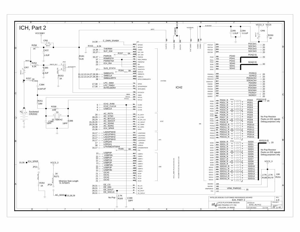
15
ICH, PART 2
10KR151
SDD15_RSDD14_RSDD13_RSDD12_RSDD11_RSDD10_RSDD9_RSDD8_RSDD7_RSDD6_RSDD5_RSDD4_RSDD3_RSDD2_RSDD1_RSDD0_R
PDD15_RPDD14_RPDD13_RPDD12_RPDD11_RPDD10_RPDD9_RPDD8_RPDD7_RPDD6_RPDD5_RPDD4_RPDD3_RPDD2_RPDD1_RPDD0_R
20SIORDY20PIORDY20SDIOW#20PDIOW#20SDIOR#20PDIOR#20SDDACK#20PDDACK#20SDREQ20PDREQ
SDA0SDA1SDA2
20SDA[2:0]
PDA0PDA1PDA2
20PDA[2:0]
VRTC
C_DWN_ENAB#14,38
THERM#14,38SLP_S3#33,37 20SDCS#3
20PDCS#320SDCS#120PDCS#1
PWROK33,37RSMRST#37
36 PWRBTN#ICH_RI#23
17 SUS_STAT#
11,12,13,14,27,28,38 SMBDATA
11,12,13,14,27,28,38 SMBCLKSMBALERT#38
LPC_SMI#17,38LPC_PME#17,38INTRUDER#
RTCRST#
VBIAS
RTCX1RTCX2
ICH2_3V6666 ICH2_CLK14
6 USBCLK
28 AC_RST#
28,29 AC_SYNC
28,29 AC_BITCLK
15,28,29 AC_SDOUT
28,29,38 AC_SDIN0
28,38 AC_SDIN1
15,36 ICH_SPKR
16,17 LAD0/FWH0
16,17 LAD1/FWH1
16,17 LAD2/FWH2
16,17 LAD3/FWH3
17 LDRQ#0LDRQ#138LFRAME#/FWH416,17
USBP0P21USBP0N
21 USBP1P21USBP1N21USBP2P21USBP2N21USBP3P21USBP3N21OC#021
21 OC#1OC#221OC#321
EE_CS28,3128,31 EE_DIN
ICH5VREF
EE_DOUT28,31EE_SHCLK28,31
4,14
,38
VC
MO
S
0K
RP68
RP69
0K
0K
RP70
0K
RP71
SDD[15:0]20SDD0
SDD1SDD2SDD3SDD4SDD5SDD6SDD7SDD8SDD9SDD10SDD11SDD12SDD13SDD14SDD15
0K
RP60
R1802.7K
R259
10MY4
32.768KHZ
CR6
BA
T17
R2641K
1.0UFC285
0.1UFC284
ICH_SPKR15,36
JP21
JP24
15,28,29AC_SDOUT
R257 1K
C384
0.047UF
R252
8.2K
BA
T17
CR7
JP20
1K
R258 BAT17
CR8
VBATC
VBATC_DLY
JP13
_PD
JP14
_PU
R_VBIAS
JP24
_PD
C38618PF
C28918PF
2.2UF
C385
18PFC380
X2
VB
AT
1.0UF
C422
10MR251
R2501K
0KR157
R164 0K
R165 0K
PDD15PDD14PDD13PDD12
PDD9PDD8PDD7PDD6PDD5PDD4PDD3PDD2PDD1PDD0 20
PDD[15:0]
PDD10PDD11
0K
RP56
RP55
0K
0K
RP34
1KR253
8.2KR181
R2711K
R1832.7K
8.2KR153
35VRM_PWRGD
2.7KR179
U17
1
2
3
45
6
7
88
7
6
5 4
3
2
1
1
2
3
45
6
7
8 1
2
3
45
6
7
8
1
2
3
45
6
7
88
7
6
5 4
3
2
1
1
2
3
45
6
7
8 1
2
3
45
6
7
8
1
2
3
45
6
7
88
7
6
5 4
3
2
1
VCC5DUAL
VCC3_3
VCC3_3 VCC5
1 2
C
A
A
C
1
2
33
2
1
CA
+2
1
+2 13
VCC3SBY
B
C
D
8 7 6 5 4 3 2 1
D
C
B
A
345678
A
2 1OFFOLSOM, CA 95630
1900 PRAIRIE CITY RD
PROJECT:
REV:
DRAWN BY:
SHEET:LAST REVISED:
PCG PLATFORM DESIGNINTEL (R) PCG
42
1.0INTEL(R) 82815E CUSTOMER REFERENCE BOARD
R
12-17-99
VCC3_3
1
2
3
45
6
7
8 1
2
3
45
6
7
8
1
2
3
45
6
7
88
7
6
5 4
3
2
1
1
2
3
45
6
7
8 1
2
3
45
6
7
8
SYSTEM
LPC
AC97
IDE
ICH2
USB
VC
C1_
8SB
Y;H
5,J5
,V14
,V15
,V16
U20TP0
AC_BIT_CLKR19
V22 AC_RST#
Y22 AC_SDIN0
AC_SDIN1W22
AC_SDOUTP21
AC_SYNCP19
CLK14M19
P20 CLK48
D4 CLK66
EE_CSK4
K3 EE_DIN
EE_DOUTJ4
J3 EE_SHCLK
FS0AA12
GPIO11/SMBALERT#AB17
GPIO24V21
W15 GPIO25
GPIO5/PIRQH#M4
GPIO6Y11
T19 INTRUDER#
Y12 LAD0/FWH0
LAD1/FWH1W12
AB13 LAD2/FWH2AB12 LAD3/FWH3
LDRQ0#Y13
LDRQ1#W13
LFRAME#/FWH4AB11
OC0#W19
Y20 OC1#
OC2#Y21
W20 OC3#
PDA0 F20
PDA1F19
PDA2 E22
PDCS1# E21
PDCS3# E19
PDD0 H19
PDD1 H22
PDD10 K22
K20PDD11J21
PDD12
J20PDD13
PDD14 H21
PDD15 H20
J19PDD2J22PDD3K21PDD4
PDD5L20
PDD6 M21
PDD7M22
L22PDD8
PDD9 L21
F22PDDACK#
PDDREQ G22
PDIOR# G19
PDIOW# G21
PIORDY G20
PWRBTN#W21
PWROKR20
RI#AA17
R21 RSMRST#
RSM_PWROKY16
T20 RTCRST#
U22 RTCX1
RTCX2T22
SDA0 A16
SDA1 D16
SDA2 B16
SDCS1# C15
SDCS3# D15
SDD0 D18
SDD1 B19
D20SDD10B20SDD11C19SDD12A19SDD13
SDD14 C18
SDD15 A18
SDD2 D19
A20SDD3C20SDD4C21SDD5D22SDD6
SDD7 E20
SDD8 D21
C22SDD9
SDDACK# B17
SDDREQ B18
SDIOR# D17
SDIOW# C17
SIORDY A17
SLP_S3#W16
AB18 SLP_S5#
SMBCLKAB16
AA16SMBDATA
SMLINK0 U19
V20SMLINK1
N22 SPKR
AA18 SUSCLK
Y17 SUSSTAT#
THRM#AA13
W17 USBP0+Y18 USBP0-
USBP1+AB19
AA19 USBP1-W18 USBP2+
USBP2-Y19
AB20 USBP3+AA20 USBP3-
K2
V5R
EF
1
V5R
EF
2M
20
V19
V5R
EF
_SU
S
T21 VBIAS
D12
VC
CP
U1
D13
VC
CP
U2
VC
CR
TC
U21
VC
C3S
BY
;F5,
G5,
T18
,U18
,V17
,V18
B15VRMPWRGD B15
D13
D12
F19
U21
F20
B16
D16
E22
V21
W16
AA13
V19
V20
G21
D17
G19
E21
C15
R20
AB13
W12
AB11
U19K4
K3
K2
Y20
W19
W13
AB12
Y13
W22
M4
Y11
R21
W15
Y17
C22
D21
D22
E20
D19
C20
A20
H19
AB18
W21
AA17
AB17
T19
T20
V22
C17
B17
F22
D15
E19
L20
M22
A18
C18
A19
C19
B20
D20
C21
B19
D18
U22
H20
H21
J20
J21
K20
K22
L21
L22
M21
K21
J22
J19
H22
A17
G20
B18
G22
A16
Y12
T22
T21
AA18
D4
AA16
M19
Y22
P21
P20
P19
N22
W17
AA19
Y18
AB19
AB16
R19
Y21
W20
AB20
Y19
AA20
W18
M20
J3
J4
AA12
Y16
No Pop ResistorPacks on IDE signalsDebug purposes only
to Jumpers
SocketedCR2032
ICH, Part 2
Minimize Stub Length
No Pop
Debug purposes onlyPacks on IDE signalsNo Pop Resistor

16
FIRMWARE HUB (FWH)
TBLK_LCK
8.2K
RP65
PCLK_6
7,10,14,17,18,19,20,26 PCIRST#
15,17LAD0/FWH015,17LAD1/FWH115,17LAD2/FWH215,17LAD3/FWH3
4,14INIT#
WPROT
0KR273
C425
0.1UF 0.1UF
C401 C424
0.1UF
C423
0.1UF
C387
0.1UF
C395
0.1UF
40PIN_TSOP_SKTX3
R_VPP
FG
PI2
_PD
IC_P
DF
GP
I4_P
DF
GP
I3_P
D
LFRAME#/FWH4 15,17
8.2K
RP64
4.7K
R274
FG
PI0
_PD
FG
PI1
_PD
JP26
4.7KR288
12345 6 7 8
12345 6 7 8
VCC3_3
VCC3_3
VCC3_3VCC3_3
1 NC1
NC33
NC44
5 NC5
NC66
8 NC8
IC2
CLK9
VCC1010
VPP11
RST#12
13 NC13
NC1414
WP#19
TBL#20 21ID3
ID2 22ID1
23ID0 24
FWH0 25FWH1 26FWH2 27FWH3 28
GND29 29GND30 30VCC31 31RFU32 32
33RFU33
34RFU34
RFU35 35RFU36 36
INIT# 37FWH4 38VCCA 39
40GNDA
7FGPI4
FGPI315
16 FGPI2
FGPI117
18FGPI0
18
17
16
15
7
40
39
38
37
36
35
34
33
32
31
30
29
28
27
26
25
24
23
22
2120
19
14
13
12
11
10
9
2
8
6
5
4
3
1
12345 6 7 88765
4 3 2 1
VCC3_3
B
C
D
8 7 6 5 4 3 2 1
D
C
B
A
345678
A
2 1OFFOLSOM, CA 95630
1900 PRAIRIE CITY RD
PROJECT:
REV:
DRAWN BY:
SHEET:LAST REVISED:
PCG PLATFORM DESIGNINTEL (R) PCG
42
1.0INTEL(R) 82815E CUSTOMER REFERENCE BOARD
R
12-17-99
Distribute close to each power pin.
FirmWare Hub (FWH) SocketNOTE: This is a TSOP Implementation
OUTIN Unlocked
JP26 Top Block Lock
Locked
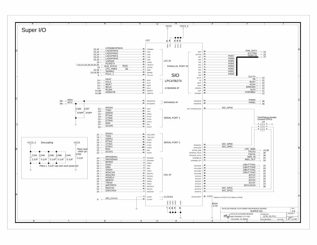
17
SUPER I/O
15 SUS_STAT#
IRRX36
470PF
C397
IRTX36
J25
23 DCD#123 RI#123 DTR#1
23 RTS#123 DSR#1
23 CTS#1
15,16 LAD3/FWH3
15,16 LAD2/FWH2
15,16 LAD1/FWH1
15,16 LAD0/FWH0
15 LDRQ#0
7,10,14,16,18,19,20,26 PCIRST#
15,38 LPC_PME#
14,19,38 SERIRQ
6 PCLK_1
14,38 RCIN#
14,38 A20GATE
23 RXD#0
23 TXD0
23 DSR#0
23 RTS#0
23 CTS#0DTR#0
2323 RI#0
DCD#023
24DRVDEN#1
24DRVDEN#0
24 MTR#0
24 DS#0
24 DIR#
24 STEP#
24 WDATA#
24 WGATE#
24HDSEL#
24 INDEX#
24 TRK#0
24WRTPRT#
JOY2Y 2525JOY2X25JOY1Y25JOY1X25J2BUTTON225J2BUTTON125J1BUTTON225J1BUTTON1
25MIDI_OUTMIDI_IN 25
36TACH136TACH2
36PWM1 36PWM2
STROBE#2222ALF#22ERROR#22ACK#22BUSY22PE22SLCT#
22PDR[7:0]PDR6PDR5PDR4
PDR2PDR1PDR0
PDR7
PDR3
22SLCTIN#
24 RDATA#
22PAR_INIT#
24 DSKCHG#
6 SIO_CLK14
SIO_GP43
SIO_GP21SIO_GP22
15,38LPC_SMI#
2.2UF
C341 C388
0.1UF 0.1UF
C345
SIO_GP61
TXD123
C340
0.1UF 0.1UF
C390 C336
0.1UF
470PF
C389
SYSOPT
SIO_GP60
KEYLOCK# 36
RXD#123
24 KCLK24 KDAT
24 MDAT
24 MCLK
15,16 LFRAME#/FWH4
R2244.7K
R231
0K
U22
5
1
3
2
4
66
4
2
3
1
5
VCC5VCC3_3
VCC5
+2
1
VCC3_3
SIOLPC47B27X
A20GATE64
ACK# 80
ALF# 82
40A
VS
S
BUSY 79
CLKI326
CLOCKI19
CTS1#88
99 CTS2#
DCD1#91
94 DCD2#
DIR#8
DRVDEN01DRVDEN12
DS0#5
DSKCHG#4
DSR1#86
DSR2#97
DTR1#89
100 DTR2#
ERROR# 81
FAN1/GP33 55FAN2/GP32 54
FDC_PP/DDRC/GP43 28
GN
D1
7
GN
D2
31
GN
D3
60 76G
ND
4
GP10/J1B1 32
GP11/J1B2 33
GP12/J2B1 34
GP13/J2B2 35
GP14/J1X 36
GP15/J1Y 37
GP16/J2X 38
GP17/J2Y 39
GP20/P17 41
GP21/P16 42
GP22/P12 43
GP25/MIDI_IN 46
GP26/MIDI_OUT 47
GP27/IO_SMI# 50
GP30/FAN_TACH2 51
GP31/FAN_TACH1 52
GP60/LED1 48
GP61/LED2 49
HDSEL#12
INDEX#13
INIT# 66
IRRX2/GP3461
IRTX2/GP3562
KBDRST63
KCLK57KDAT56
LAD020LAD121LAD222LAD323
LDRQ#25
LFRAME#24
LRESET#26
MCLK59MDAT58
MTR0#3
PCI_CLK29 PD0 68PD1 69PD2 70PD3 71PD4 72PD5 73PD6 74PD7 75
PE 78
PME#17
RDATA#16
RI1#90
92 RI2#
RTS1#87
RTS2#98
RXD184
RXD2_IRRX95
SERIRQ30
SLCT# 77
SLCTIN# 67
STEP#9
STROBE# 83
TRK0#14
TXD185
TXD2_IRTX96
VC
C1
53
VC
C2
65
VC
C3
93
WDATA#10
WGATE#11
WRTPRT#15
44V
RE
F
GP24/SYSOPT 45
VT
R18
LPCPD#27
SERIAL PORT 1
SERIAL PORT 2
FDC I/F
LPC I/F
INFRARED I/F
CLOCKS
KYBD/MSE I/F
PARALLEL PORT I/F27
18
45
44
15
11
10
936553
96
85
14
83
9
67
77
30
95
84
98
87
92
90
16
17
78
75
74
73
72
71
70
69
6829
3
58
59
26
24
25
23
22
21
20
56
57
63
62
61
66
13
12
49
48
52
51
50
47
46
43
42
41
39
38
37
36
35
34
33
32
7660317
28
54
55
81
100
89
97
86
4
5
2
1
8
94
91
99
88
19
6
79
40
82
80
64
B
C
D
8 7 6 5 4 3 2 1
D
C
B
A
345678
A
2 1OFFOLSOM, CA 95630
1900 PRAIRIE CITY RD
PROJECT:
REV:
DRAWN BY:
SHEET:LAST REVISED:
PCG PLATFORM DESIGNINTEL (R) PCG
42
1.0INTEL(R) 82815E CUSTOMER REFERENCE BOARD
R
12-17-99
Pulldown on SYSOPT for IO address of 0x02E
Decoupling
Place nearVREF pin
Place 1 0.1UF cap near each power pin
Test/Debug HeaderUnused GPIOs
Super I/O
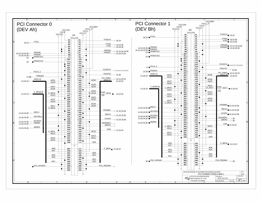
18
PCI CONNECTORS 0 AND 1
AD17 14,18,19
14,18,19AD16
J20
AD0AD2
AD4AD6
AD9
AD11AD13
AD15
AD16AD18
AD20AD22
AD24
AD26AD28
14,18,19AD[31:0]AD30
38PU2_REQ64#
C_BE#0 14,18,19
14,18,19PAR
38SBOP238SDONEP2
14,18,19,38FRAME#
PCI_PME# 10,14,18,19
PGNT#114,38
10,14,18,19,38 PIRQ#A
AD31AD29
AD27AD25
AD23
AD21AD19
AD17
AD14
AD12AD10
AD8AD7
AD5AD3
AD1
14,18,19AD[31:0]
C_BE#3
C_BE#2
C_BE#1
14,18,19C_BE#[3:0]
19 PRSNT#22
19 PRSNT#21
18,19PTRST#
PTMS 18,19,3818,19,38PTDI
PIRQ#B 10,14,18,19,3814,18,19,38PIRQ#D
PCIRST#7,10,14,16,17,18,19,20,26
R_AD17
14,18,19,38TRDY#
14,18,19,38STOP#
14,18,19,38 SERR#
14,18,19,38 PERR#14,18,19,38 PLOCK#
14,18,19,38 DEVSEL#
14,18,19,38 IRDY#
14,38 PREQ#1
6 PCLK_3
14,18,19,38 PIRQ#C
PTCK18,19
18,19 PTCK
PIRQ#B10,14,18,19,38
PCLK_2
IRDY#14,18,19,38
DEVSEL#14,18,19,38
PLOCK#14,18,19,38PERR#14,18,19,38
SERR#14,18,19,38
STOP# 14,18,19,38
TRDY# 14,18,19,38
R_AD16
7,10,14,16,17,18,19,20,26PCIRST#
PIRQ#C 14,18,19,3810,14,18,19,38PIRQ#A
PTDI 18,19,3818,19,38PTMS
PTRST# 18,19
PRSNT#1119
PRSNT#1219
C_BE#[3:0]14,18,19
C_BE#2
C_BE#1
C_BE#3
AD[31:0]14,18,19
AD29
AD25
AD23
AD19
AD17
AD14
AD10
AD8AD7
AD5AD3
AD1
AD31
AD27
AD21
AD12
PIRQ#D14,18,19,38
PU1_ACK64#
14,38PGNT#0
10,14,18,19PCI_PME#
FRAME# 14,18,19,38
SDONEP1SBOP1
PAR 14,18,19
14,18,19C_BE#0
PU1_REQ64#
AD0AD2
AD4AD6
AD9
AD11AD13
AD15
AD16AD18
AD20AD22
AD24
AD26AD28
AD30 AD[31:0] 14,18,19
38 PU2_ACK64#
J19
PREQ#014,38
R184
100
100
R185
PCI3_CON
A2
A21
A27
A33
A39
A45
B25
B31
B36
B41
B43
A53B54
A5
A10
A16
B5B6
A59
A61A62
B61
B19
B1
B60
A58B58
B48A47B47A46
B45
B32A31
B30A29B29
B27
A25B24B23
A22B21
B56
B20
A55B55A54
B53B52
A49
A52
B44
B33
B26
B16
A9
B37
A34
A12A13
A18
A24
A30
A35
A37
A42
A48
B3
B12B13
B15
B17
B22
B34
B38
B46
B49
A56B57
B28
A17
A26
A6B7 A7B8
B35
B39
A43
B40
B9
B11
B2
B4 A4A3
A1
B18
A60
A11
A14
B10
B14A15
A41A40
B42
A36
A57
A44
B59
A38
A32
A28
A8
B62
A19A20
A23
key
A2
A21
A27
A33
A39
A45
B25
B31
B36
B41
B43
A53B54
A5
A10
A16
B5B6
A59
A61A62
B61
B19
B1
B60
A58B58
B48A47B47A46
B45
B32A31
B30A29B29
B27
A25B24B23
A22B21
B56
B20
A55B55A54
B53B52
A49
A52
B44
B33
B26
B16
A9
B37
A34
A12A13
A18
A24
A30
A35
A37
A42
A48
B3
B12B13
B15
B17
B22
B34
B38
B46
B49
A56B57
B28
A17
A26
A6B7 A7B8
B35
B39
A43
B40
B9
B11
B2
B4 A4A3
A1
B18
A60
A11
A14
B10
B14A15
A41A40
B42
A36
A57
A44
B59
A38
A32
A28
A23
A8
B62
A19A20
VCC3SBYVCC3_3
VCC5VCC12
VCC12MVCC5
VCC3_3
VCC3_3VCC5
VCC12M
VCC12VCC5
VCC3_3VCC3SBY
PCI3_CON
A2
A21
A27
A33
A39
A45
B25
B31
B36
B41
B43
A53B54
A5
A10
A16
B5B6
A59
A61A62
B61
B19
B1
B60
A58B58
B48A47B47A46
B45
B32A31
B30A29B29
B27
A25B24B23
A22B21
B56
B20
A55B55A54
B53B52
A49
A52
B44
B33
B26
B16
A9
B37
A34
A12A13
A18
A24
A30
A35
A37
A42
A48
B3
B12B13
B15
B17
B22
B34
B38
B46
B49
A56B57
B28
A17
A26
A6B7 A7B8
B35
B39
A43
B40
B9
B11
B2
B4 A4A3
A1
B18
A60
A11
A14
B10
B14A15
A41A40
B42
A36
A57
A44
B59
A38
A32
A28
A8
B62
A19A20
A23
key
A20
B62
A8
A23
A28
A32
A38
B59
A44
A57
A36
B42
A40A41
A15B14
B10
A14
A11
A60
B18
A1
A3A4B4
B2
B40
A43
B39
B35
B8A7B7A6
A26
A17
B28
B57A56
B49
B46
B38
B34
B22
B17
B15
B13B12
B3
A48
A42
A37
A35
A30
A24
A18
A13A12
A34
B37
A9
B16
B52B53
A54B55 A55
B20
B56
B21A22
B23B24
A25
B27
B29 A29B30
A31B32
B45A46
B47 A47B48
B58 A58
B60
B1
B19
B61A62A61
A59
B6B5
A16
A10
A5
B54A53
B43
B41
B36
B31
B25
A45
A39
A33
A27
A21
A2
B
C
D
8 7 6 5 4 3 2 1
D
C
B
A
345678
A
2 1OFFOLSOM, CA 95630
1900 PRAIRIE CITY RD
PROJECT:
REV:
DRAWN BY:
SHEET:LAST REVISED:
PCG PLATFORM DESIGNINTEL (R) PCG
42
1.0INTEL(R) 82815E CUSTOMER REFERENCE BOARD
R
12-17-99
(DEV Ah)PCI Connector 0
(DEV Bh)PCI Connector 1

19
PCI CONNECTOR 2
14,18,19AD22
C105
0.1UF
19 PRSNT#31
PRSNT#3219
18 PRSNT#11
PRSNT#2218
PRSNT#1218
PRSNT#2118
19 PRSNT#32
18,19 PTCK
PIRQ#D14,18,38
PCLK_46
PREQ#214,38
IRDY#14,18,38
DEVSEL#14,18,38
PLOCK#14,18,38PERR#14,18,38
SERR#14,18,38
STOP# 14,18,38
TRDY# 14,18,38
R_AD22
PIRQ#A 10,14,18,3814,18,38PIRQ#C
PTDI 18,3818,38PTMS
PTRST# 18,19
PRSNT#3119
C_BE#1
C_BE#2
C_BE#3C_BE#[3:0]14,18
AD1
AD3AD5
AD7AD8
AD10AD12
AD14
AD17
AD19AD21
AD23
AD25AD27
AD29AD31
AD[31:0]14,18,19
PIRQ#B10,14,18,38
PU3_ACK64#38
14,38PGNT#2
10,14,18PCI_PME#
FRAME# 14,18,38
SDONEP3 38SBOP3 38
PAR 14,18
14,18C_BE#0
PU3_REQ64# 38
AD[31:0]14,18,19
AD28AD26
AD24
AD22AD20
AD18AD16
AD15
AD13AD11
AD9
AD6AD4
AD2AD0
AD30
7,10,14,16,17,18,20,26PCIRST#
R189
14,17,38 SERIRQ
14,38 GPIO210K
R199
PTRST#18,19
18,19 PTCK
C100
0.1UF 0.1UF
C101 C102
0.1UF 0.1UF
C103 C104
0.1UF
J22
5.6K
R187
R188
5.6K
R200
0K
0K
R201 PCPCI_REQ#A14,38
VAUX3R_SERIRQ
R_GNT#A
0K
R198
R_GPO21
PCPCI_GNT#A 14
R202
100
VCC3_3VCC5
VCC12M
VCC12VCC5
VCC3_3
0K
PCI3_CON
A2
A21
A27
A33
A39
A45
B25
B31
B36
B41
B43
A53B54
A5
A10
A16
B5B6
A59
A61A62
B61
B19
B1
B60
A58B58
B48A47B47A46
B45
B32A31
B30A29B29
B27
A25B24B23
A22B21
B56
B20
A55B55A54
B53B52
A49
A52
B44
B33
B26
B16
A9
B37
A34
A12A13
A18
A24
A30
A35
A37
A42
A48
B3
B12B13
B15
B17
B22
B34
B38
B46
B49
A56B57
B28
A17
A26
A6B7 A7B8
B35
B39
A43
B40
B9
B11
B2
B4 A4A3
A1
B18
A60
A11
A14
B10
B14A15
A41A40
B42
A36
A57
A44
B59
A38
A32
A28
A8
B62
A19A20
A23
key
A20
B62
A8
A23
A28
A32
A38
B59
A44
A57
A36
B42
A40A41
A15B14
B10
A14
A11
A60
B18
A1
A3A4B4
B2
B40
A43
B39
B35
B8A7B7A6
A26
A17
B28
B57A56
B49
B46
B38
B34
B22
B17
B15
B13B12
B3
A48
A42
A37
A35
A30
A24
A18
A13A12
A34
B37
A9
B16
B52B53
A54B55 A55
B20
B56
B21A22
B23B24
A25
B27
B29 A29B30
A31B32
B45A46
B47 A47B48
B58 A58
B60
B1
B19
B61A62A61
A59
B6B5
A16
A10
A5
B54A53
B43
B41
B36
B31
B25
A45
A39
A33
A27
A21
A2
VCC3SBY
B
C
D
8 7 6 5 4 3 2 1
D
C
B
A
345678
A
2 1OFFOLSOM, CA 95630
1900 PRAIRIE CITY RD
PROJECT:
REV:
DRAWN BY:
SHEET:LAST REVISED:
PCG PLATFORM DESIGNINTEL (R) PCG
42
1.0INTEL(R) 82815E CUSTOMER REFERENCE BOARD
R
12-17-99
For Debug Only
For Debug Only
For Debug Only
For Debug OnlyDo Not Stuff R192
PCI Connector 2(DEV 6h)
Layout Note: Should be in Slot 0 Position (Outside Edge of Board Furthest from CPU)

20
ULTRA DMA/66 CONNECTORS
7,10,14,16,17,18,19,26 PCIRST# 20PCIRST_BUF#
4.7KR100
4.7KR102
33
R190J15
SECONDARYIDE CONN.
J16
PRIMARYIDE CONN.
PDIOW#15PDIOR#15PIORDY15
SDIOW#15
SIORDY15PDDACK#15 SDDACK#15
SDCS#3 1515PDCS#3
IRQ1514,38IRQ1414,38
IDEACTP#36
PDCS#115
15PDA[2:0]
PDA0PDA1
PDA2
SDCS#115
20PCIRST_BUF#
SDIOR#15
R182
33R_RSTP# R_RSTS#
R1918.2KU11
20PCIRST_BUF#
15 PDREQ
15SDA[2:0]
SDA1SDA0
SDA2
IDEACTS#36
15 SDREQ
SDD7SDD6SDD5SDD4SDD3SDD2SDD1SDD0
15
SDD8SDD9SDD10SDD11SDD12SDD13SDD14SDD15
SDD[15:0]
P66DETECT 14 S66DETECT 14
PDD7PDD6PDD5PDD4PDD3PDD2PDD1PDD0
PDD8PDD9PDD10PDD11PDD12PDD13PDD14
15PDD[15:0]
PDD15
1
10
11 12
13 14
15 16
17 18
19
2
20
21 22
23 24
25 26
27 28
29
3
30
31 32
33 34
35 36
37 38
39
4
40
5 6
7 8
9
1
10
11 12
13 14
15 16
17 18
19
2
20
21 22
23 24
25 26
27 28
29
3
30
31 32
33 34
35 36
37 38
39
4
40
5 6
7 8
9
1
10
11 12
13 14
15 16
17 18
19
2
20
21 22
23 24
25 26
27 28
29
3
30
31 32
33 34
35 36
37 38
39
4
40
5 6
7 8
99
87
65
40
4
39
3837
3635
3433
3231
30
3
29
2827
2625
2423
2221
20
2
19
1817
1615
1413
1211
10
1
VCC3_3
VCC3_3
SN74LVC07AGND
VCC14
7
5 6
B
C
D
8 7 6 5 4 3 2 1
D
C
B
A
345678
A
2 1OFFOLSOM, CA 95630
1900 PRAIRIE CITY RD
PROJECT:
REV:
DRAWN BY:
SHEET:LAST REVISED:
PCG PLATFORM DESIGNINTEL (R) PCG
42
1.0INTEL(R) 82815E CUSTOMER REFERENCE BOARD
R
12-17-99
VCC3_3VCC3_3
IDE Connectors

21
10 AGP_OC# R308
0K
R31
0
330K
28 CNR_OC#
R30
7
330K
USB_V5_2
USB_V5_1OC#1
15
USB_D3_P
R301
0K
0K
R302
0K
R296
USB_D1_N
USB_D0_N
.1UF
C52
68UF
C81
L26
L27
100KR26
8
68UF
C83
.1UF
C53
R284
15
15
R285
15
R256
R260
15
.1UF
C51
68UF
C54
POLYSWITCH_RUSB250-1
2.5AF1
100KR26
1
L25
USB_D0_P
47PF
C47
47PF
C50
47PF
C43
47PF
C45C41
47PF
C42
47PF
L2347PF
C33
47PF
C40
L24
L2147PF
C7
USB_GND_3
J2
L20
15K
R19
4
15K
R19
5
R19
2
15K
R15
8
15K
100KR18
6
POLYSWITCH_RUSB250-02.5AF
3
J17
68UF
C294
47PF
C26
L10
J21
R19
315K
R19
6
15K
R15
2
15K15K
R19
7
47PF
C331
47PF
C330
15
R216
USB_GND_2
R265
15
15
R266
R298
0K
0K
R286
R287
0KUSB_D2_N
R299
0K
USB_GND_1
USB_D3_N
USB_GND_0
0K
R300
28CNR_USB-
10 AGPUSBN10AGPUSBP
POLYSWITCH_RUSB250-2
2.5AF4
15
R215
OC#015 USB_V5_0R303
10K
10K
R304
R305
10K
R306
0K
15OC#2
R26
7
100K
USB_V5_315OC#3
10K
R309
POLYSWITCH_RUSB250-3
2.5AF5
USB_D2_P
USB_D1_P
USB_PO_1
USB_PO_2
USB_PO_3
USB_PO_0
28CNR_USB+
USBP0N15 USBP0P15
USBP1N15USBP1P15
USBP3N15USBP3P15
15 USBP2NUSBP2P
15
.1UF
C295
VCC3_3SBY
VCC3_3SBY
2
1
+1
2
1 21 2
1 221
+2
1
1
2
2
1
+1
2
12
12
1 21 2
2
1 1
22
11
2
1
22
1
12
12
2
1
1
2
122
1 12
12
2
1
3 DATA1+
2 DATA1-
7 DATA2+
6 DATA2-
4GND1
8 GND2
5 VCC2
RJMAG_USB
1 VCC11
5
8
4
6
7
2
3
1 2211
221
1
2
3
44
3
2
1
VCC5DUAL
B
C
D
8 7 6 5 4 3 2 1
D
C
B
A
345678
A
2 1OFFOLSOM, CA 95630
1900 PRAIRIE CITY RD
PROJECT:
REV:
DRAWN BY:
SHEET:LAST REVISED:
PCG PLATFORM DESIGNINTEL (R) PCG
42
1.0INTEL(R) 82815E CUSTOMER REFERENCE BOARD
R
12-17-99
+2
1
1
2
122
1
1
2
3
44
3
2
1
1
2 2
1
12
12
122
1
1
2
15 ohm resistors should be < 1" from ICH2
15 ohm resistors should be < 1" from ICH2
15 ohm resistors should be < 1" from ICH2
Do notpopulate
populate
Do not
USB Hub
USB Hub and Connectors
Do notpopulate
Do not
15 ohm resistors should be < 1" from ICH2
populate
47pf caps should be < 1" from ICH2

PARALLEL PORT
22
J8
C215
180P
F
C214
180P
F
180P
F
C207
C187
180P
F
180P
F
C168
C167
180P
F
180P
F
C166
C165
180P
F
180P
F
C175
C164
180P
F
180P
F
C176
180P
F
C170
RP38
33
RP41
33
PDR2
PDR3
PDR7
PDR[7:0]17
PDR6
PDR5
PDR4
PDR0
PDR1
RP402.2K 2.2K
RP42
VCC5_DB25_CR
PE17
BUSY17
ACK#17
17 SLCTIN#
STROBE#17
PAR_INIT#17
ERROR#17
ALF#17
RP462.2K
RP392.2K
R842.2K
CR3
1N4148
33
RP63
C172
180P
F
C171
180P
F
180P
F
C178
180P
F
C163
C17718
0PF
17 SLCT#DB25
13
25
12
24
11
23
10
22
9
21
8
20
7
19
6
18
5
17
4
16
3
15
2
14
11
14
2
15
3
16
4
17
5
18
6
19
7
20
8
21
9
22
10
23
11
24
12
25
13
1
2
3
4 5
6
7
88
7
6
54
3
2
1
1
2
3
4 5
6
7
81
2
3
4 5
6
7
8
VCC5
1 2 3 45678
1 2 3 45678
1 2 3 45678
1 2 3 45678
1 2 3 45678 8 7 6 5
4321
1 2 3 456788 7 6 5
4321
A C
1
2
3
4 5
6
7
88
7
6
54
3
2
1
B
C
D
8 7 6 5 4 3 2 1
D
C
B
A
345678
A
2 1OFFOLSOM, CA 95630
1900 PRAIRIE CITY RD
PROJECT:
REV:
DRAWN BY:
SHEET:LAST REVISED:
PCG PLATFORM DESIGNINTEL (R) PCG
42
1.0INTEL(R) 82815E CUSTOMER REFERENCE BOARD
R
12-17-99
Parallel Port
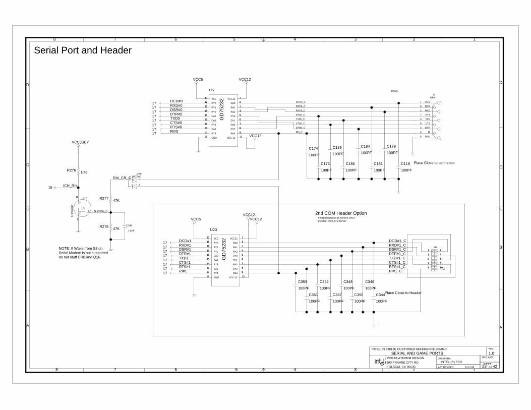
23
SERIAL AND GAME PORTS
J7
DCD#017RXD#017DSR#017DTR#017
17TXD0CTS#0
17 RTS#017
RTS0_C
CTS0_C
TXD0_C
DTR0_C
RI#017
DSR0_C
RXD0_C
DCD0_C
100PF
C179
C398
1.0UF
10KR276
R278 47K
15 ICH_RI#
C344
100PF
C346
100PF
100PF
C350
C348
100PF
100PF
C347
C352
100PF100PF
C353
100PF
C351
CTS#117
DSR#1_C
DCD#1_C
TXD#1_CDTR#1_C
17 TXD117 DTR#117 DSR#1
17 DCD#1
17 RTS#1RI#117
RXD#1_C
CR9
47KR277
RTS#1_CCTS#1_C
RI#_CR_C
17 RXD#1
ICHRI#_C
Q16
J32
100PF
C174
C173
100PF
100PF
C189
C186
100PF
100PF
C184
C181
100PF 100PF
C118
U5
RI0_C
U23
RI#1_C
DB9
DCD
DSR
RXD
RTS
TXD
CTS
DTR
RI
GND5
9
4
8
3
7
2
6
1
VCC12
VCC12-
VCC5
VCC3SBY
VCC5
BAT54C3
2
1
VCC12VCC12-
2N7002LT
1
G1
D
3
S
2
S
D
G
1
10
2
3
5 6
7 8
9
4
1
10
2
3
5 6
7 8
9
4
DA016
DA115
DA213
DY0 5
DY1 6
DY2 8
GND11
RA0 2
RA1 3
RA2 4
RA3 7
RA4 9
RY019
RY118
RY217
RY314
RY412
VCC20
VCC-12 10
VCC12 1
GD
7523
2
16
15
13
5
6
8
2
4
7
9
19
18
17
14
20
DA016
DA115
DA213
DY0 5
DY1 6
DY2 8
GND11
RA0 2
RA1 3
RA2 4
RA3 7
RA4 9
RY019
RY118
RY217
RY314
RY412
VCC20
VCC-12 10
VCC12 1
GD
7523
2
19
18
17
15
14
13
2
4
5
6
7
8
9
16
20
B
C
D
8 7 6 5 4 3 2 1
D
C
B
A
345678
A
2 1OFFOLSOM, CA 95630
1900 PRAIRIE CITY RD
PROJECT:
REV:
DRAWN BY:
SHEET:LAST REVISED:
PCG PLATFORM DESIGNINTEL (R) PCG
42
1.0INTEL(R) 82815E CUSTOMER REFERENCE BOARD
R
12-17-99
COM1
Place Close to Header
2nd COM Header Option
NOTE: If Wake from S3 on
If not populated at all, remove CR14and short RI#0_C to RI#CR
Place Close to connector
Serial Port and Header
Serial Modem is not supporteddo not stuff CR8 and Q16.
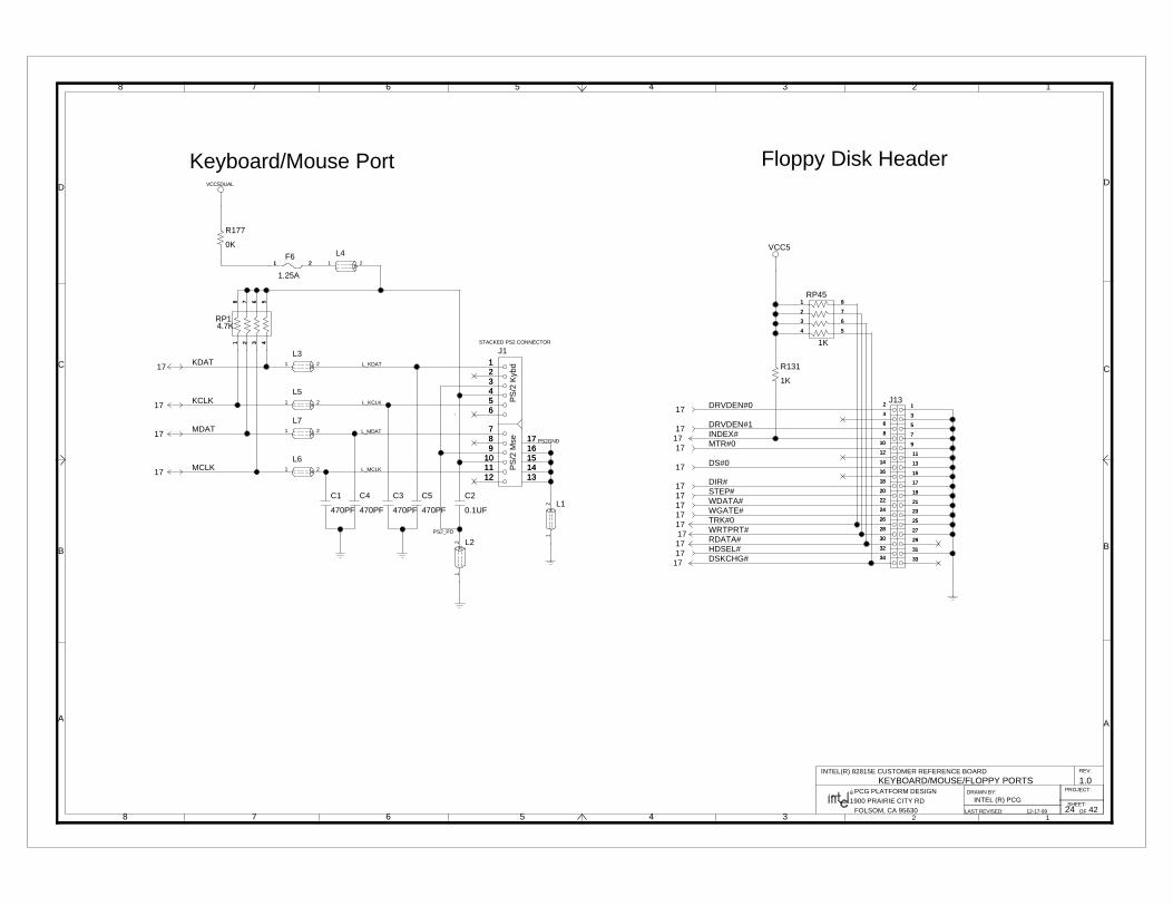
KEYBOARD/MOUSE/FLOPPY PORTS
24
0K
R177
17 MCLK
17MDAT
KDAT17
KCLK17
L2
0.1UF
C2
17 HDSEL#
17 WGATE#17 WDATA#
17 DIR#
17 STEP#
17 DSKCHG#
17 DRVDEN#0J13
17 DS#0
17 WRTPRT#
17 RDATA#
INDEX#1717 DRVDEN#1
17 TRK#0
17 MTR#0
C1
470PF 470PF
C4 C3
470PF 470PF
C5
STACKED PS2 CONNECTOR
J1L3
L5
L7
L6
4.7KRP1
L4
L1
L_MCLK
L_MDAT
L_KCLK
L_KDAT
PS2_PD
PS2GND
R131
1K
1K
RP45
1.25A
F6
12
1
10
1112
1314
1516
1718
19
2
20
2122
2324
2526
2728
29
3
30
3132
3334
4
56
78
99
8 7
6 5
4
34 33
32 31
30
3
29
28 27
26 25
24 23
22 21
20
2
19
18 17
16 15
14 13
12 11
10
1
VCC5
1
101112 13
14151617
23456
789
PS
/2 K
ybd
PS
/2 M
se
1314151617
121110987
6543211 2
1 2
1 2
1 2
1 2 3 456788 7 6 5
4321
1 2
12
VCC5DUAL
B
C
D
8 7 6 5 4 3 2 1
D
C
B
A
345678
A
2 1OFFOLSOM, CA 95630
1900 PRAIRIE CITY RD
PROJECT:
REV:
DRAWN BY:
SHEET:LAST REVISED:
PCG PLATFORM DESIGNINTEL (R) PCG
42
1.0INTEL(R) 82815E CUSTOMER REFERENCE BOARD
R
12-17-99
1
2
3
4 5
6
7
81
2
3
4 5
6
7
8
1 21 2
Keyboard/Mouse Port Floppy Disk Header
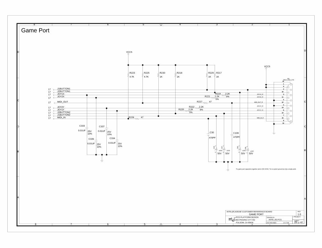
GAME PORT
25
C80
47PF
50V
10%25V
C334
0.01UF
0.01UF
C337
25V10%
R226 47
2.2KR2205%
2.2KR2225%
1K
R217R218
1K
17 MIDI_IN17 J1BUTTON217 J2BUTTON2
17 MIDI_OUT
17 J1BUTTON1
17 J2BUTTON1JOY1X_R
JOY2X_R
MIDI_OUT_R
JOY2Y_R
JOY1Y_R
MIDI_IN_R
4.7K
R223 R225
4.7K 1K
R230 R229
1K
2.2KR2195%2.2KR221
5%R227 47
17 JOY1X
10%25V
C333
0.01UF
17JOY2X
17 JOY1Y17 JOY2Y
10%25V
C335
0.01UF
C106
470PF
C30
470PF
C68
47PF
50V50V47PF
C67
C29
47PF
50V
J30
VCC5
+2
1
+1
2
+1
2
+2
1
VCC5
DB15_AUD_STK
2
10
3
11
4
12
5
13
6
14
7
15
8
1
9
31
3232
31
9
1
8
15
7
14
6
13
5
12
4
11
3
10
2
B
C
D
8 7 6 5 4 3 2 1
D
C
B
A
345678
A
2 1OFFOLSOM, CA 95630
1900 PRAIRIE CITY RD
PROJECT:
REV:
DRAWN BY:
SHEET:LAST REVISED:
PCG PLATFORM DESIGNINTEL (R) PCG
42
1.0INTEL(R) 82815E CUSTOMER REFERENCE BOARD
R
12-17-99
Tie game port capacitors together and to SIO AVSS. Tie to system ground at only a single point.
Game Port
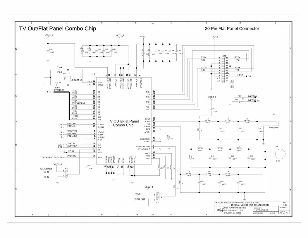
26
DIGITAL VIDEO OUT CONNECTOR
U15
0.1UF
C255
2KR22
8
1.0UF
C253
22UF
C446
.01UF
C252
.01UF
C245
22UF
C445
C227
0.1UF
L34
1.0UH
75R21
2
2.7UH
L35
330PF
C206
560PF
C208
0.68UH
L36
C119
470PF
L31
1.0UH
75R20
7
2.7UH
L32
330PF
C122
560PF
C203
0.68UH
L33
L30
0.68UH
C116
560PF
C112
330PF
L29
2.7UH
R203275VFTSDA
TX0-
TX1- TX2-
TXC+
TX1+
5VFTSCL27
CO
N_F
TS
CL
CO
N_F
TS
DA
J23
XTAL1
14.318MHZ
Y510PF
C109
10PF
C110
PCIRST#7,10,14,16,17,18,19,20
9,27 3VFTSDA
9 FTCLK1
FTD10
FTD6XREF=9FTD5
FTD4
FTD7FTD8
FTD3FTD2FTD1
FTD9
FTD0
FTD11
FTD[11:0]9
C263
1.0UF
C259
1.0UF
FTBLNK#99
FTVSYNC9FTHSYNC
9 FTCLK0
9,27 3VFTSCL
XTAL0
TX2+
TX0+
R204
1.0UH
L28
C111
470PF
22UF
C444
.01UF
C266
.01UF
C24422UF
C261
1.0UF
C262
75R20
5
R21
3
267
R21
4
10K
470PF
C205
TXC-
26HPLG
J24
J31
JP22 10KR23
2
R23
3
10K
JP23
HPLG26A0
10
AFADJ39
AV
CC
3_3[
1]47
AV
SS
42
B/PB44
2BLANK#
C/R/PR43CLKIN0
56
CLKIN157
COMP3840
CVBS
D064
D163
D1050
D1149
D262
D361
D460
D559
D654
D753
D852
D951
8D
VD
DQ
1_8
DV
SS
[0]
6 16D
VS
S[1
]D
VS
S[2
]48 58
DV
SS
[3]
18GPIO0
11HPLG
HS/CS/GPIO145
4HSYNC
35P
VD
D1_
8
PV
SS
36
13RST#
SCL15
SDA14
17TEST
19TFADJ
TV
SS
[0]
20 26T
VS
S[1
]T
VS
S[2
]32
22TX0+TX0-
2125
TX1+TX1-
2428
TX2+TX2-
2730
TXC+TXC-
31
3VREF
5VSYNC
34XTAL0XTAL1
33
Y/G41
DV
DD
3_3
12 23T
VD
D1_
8[0]
TV
DD
1_8[
1]29
AV
CC
3_3[
0]371
DV
DD
1_8[
0]D
VD
D1_
8[1]
55
46VS/FID
INT1#/CLKOUT79
INT0#/CABARE#
TV OUT/Flat PanelCombo Chip
97
46
551 37292312
41
3334
5
3
3130272824252122
322620
1917
1415
13
36
35
4
45
11 18
5848166
8
5152535459606162
4950
6364
4038
5756
43
2
44
42
4739
10
VCC3_3
VCC3_3
+1
2
+2
1
VCC3_30K
15
6 16
7 17
8 18
9 19
10 20
2 12
3
4 14
5
111
13
5
144
133
122
20
11
10
199
188
177
166
15
1
XT
AL
21
VCC1_8
B
C
D
8 7 6 5 4 3 2 1
D
C
B
A
345678
A
2 1OFFOLSOM, CA 95630
1900 PRAIRIE CITY RD
PROJECT:
REV:
DRAWN BY:
SHEET:LAST REVISED:
PCG PLATFORM DESIGNINTEL (R) PCG
42
1.0INTEL(R) 82815E CUSTOMER REFERENCE BOARD
R
12-17-99
VCC5
0K
VCC1_8
+1
2
+2
1
COMP_VIDEO
S_VID
1
2
33
2
1
VCC3_3
1
2
3
1
2
3
TV Out/Flat Panel Combo Chip 20 Pin Flat Panel Connector
I2C Address
40-41
42-43
TMDS
Video Test

27
VIDEO CONNECTOR
XREFQS4_3V
C2103.3PF
C1953.3PF
3.3PFC216
L_GREEN
3.3PFC211
3.3PFC209
3.3PFC219
MONOPU
11,12,13,14,15,28,38SMBDATA
U13
9 3VDDCCL9 3VDDCDA
275VHSYNC
11,12,13,14,15,28,38SMBCLK
R143 2.2K
R140 2.2K
9,26 3VFTSCL
9CRT_HSYNC
9CRT_VSYNC
3VFTSDA9,26
275VVSYNC
R141R142
R106751%
1%75R107
R109751%
C2133.3PF
L_RED
C25710PF
C18010PF
C24910PF
L38
FUSE_5L_HSYNCL_BLUE
MON2PU
2.2K
RP
47
275VDDCDA
5VFTSDA 26
4.7K
R13
9
3.3PFC212
0.1U
F
C25
6
L_VSYNC
C1883.3PF
0K
R85
27 5VDDCDA
1KR247
0K
R248
XREF
XREF
F2 2.5A
1KR104
BLM11B750S
L19
BLM11B750S
L18
265VFTSCL
275VDDCCL
1N4148
CR10
9 VID_RED
VID_GREEN9
27 5VHSYNC
27 5VVSYNC
9 VID_BLUE
6 CK_SMBDATA
6 CK_SMBCLK XREF
C2503.3PF
10PFC185
J9
BLM11B750S
L17
5VDDCCL27
VCC5
BEA#
2B5
2B4
2B2
2B1
1B51A5
1B41A4
1B3
1A1
1A2 1B2
2A3 2B3
BEB#
1B1
2A5
VCC
2A1
2A2
2A4
1A3
GND
QST3384
12
7
21
17
14
24
22
2
13
1918
54
3
6
8 9
11 10
15
16
20
23
1
0K
0K
12
1 2 3 456788 7 6 5
4321
122
1
1 2
1 2
C A
VCC5
10
12
13
14
15
2
4
8
9
16
117
3
5 15510
6111
10
12
13
14
15
2
4
8
9
16
117
3
5
B
C
D
8 7 6 5 4 3 2 1
D
C
B
A
345678
A
2 1OFFOLSOM, CA 95630
1900 PRAIRIE CITY RD
PROJECT:
REV:
DRAWN BY:
SHEET:LAST REVISED:
PCG PLATFORM DESIGNINTEL (R) PCG
42
1.0INTEL(R) 82815E CUSTOMER REFERENCE BOARD
R
12-17-99
1 2
VGA Connector
BLM11B750S is rated at 75Ohms at 100MHz
5V to 3.3V Translation/Isolation
Do Not Populate
Video Connector
Do Not Stuff C213 and C188
Do Not Stuff C212 and C250
Place R107,R106,&R109 Close to VGA Connector
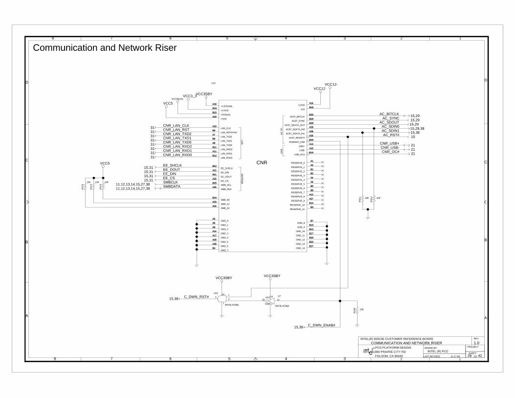
28
COMMUNICATION AND NETWORK RISER
R31
5
10K
R31
4
10K
U14
15,29,38AC_SDIN0
10K
R31
2
EE_DOUT15,3115,31
EE_SHCLK
15,31EE_DIN
15,31EE_CS
31CNR_LAN_RXD0
31CNR_LAN_RXD2CNR_LAN_TXD0
3131
CNR_LAN_TXD1
15,29AC_SDOUT
U10
AC_BITCLK 15,29AC_SYNC 15,29
21CNR_USB+
21CNR_USB-
21CNR_OC#
CNR_LAN_TXD23131 CNR_LAN_RST31 CNR_LAN_CLK
CNR_LAN_RXD131
SMBCLK11,12,13,14,15,27,38SMBDATA11,12,13,14,15,27,38
R31
1 10K
10K
R31
3
AC_SDIN1 15,38AC_RST# 15
15,38 C_DWN_RST#
15,38 C_DWN_ENAB#
R20
6 10K
U7
VCC3SBY
VCC5
US
BA
C '9
7
EE
PR
OM
LAN
CNR
GND_7B4
GND_6A30
GND_5A20
SMB_A0B24
SMB_A2A24
SMB_A1A23
GND_12B20
B3RESERVE_11
B14RESERVE_10
A27RESERVE_9
A12RESERVE_8
B6RESERVE_7
B5RESERVE_6
A5RESERVE_5
A4RESERVE_4
PRIMARY_DN#B26
B30AC97_BITCLK
B28AC97_SYNC
B29AC97_SDATA_OUT
A29AC97_SDATA_IN0
A28AC97_SDATA_IN1
A10LAN_CLK
B9LAN_RSTSYNC
A7LAN_TXD2
B8LAN_TXD1
A8LAN_TXD0
B11LAN_RXD2
A11LAN_RXD1
B12LAN_RXD0
SMB_SCLB25
SMB_SDAA25
B22EE_SHCLK
A21EE_DIN
B21EE_DOUT
EE_CSA22
A13USB+
A15USB-
A16+12VD
B18-12V
A19+5VD
B15+5VDUAL
B19+3.3VD
A3GND_0
A6GND_1
GND_2A9
GND_3A14
GND_4A17
B7GND_8
B10GND_9
GND_10B13
GND_11B17
RESERVE_0A1
RESERVE_1A2
RESERVE_2B1
RESERVE_3B2
A26AC97_RESET#
B16USB_OC#
B23GND_13
A18+3.3VDUAL
B27GND_14
B23
B16
A26
B2
B1
A2
A1
B17
B13
B10
B7
A17
A14
A9
A6
A3
A18
B19
B15
A19
B18
A16
A15
A13
A22
B21
A21
B22
A25
B25
B12
A11
B11
A8
B8
A7
B9
A10
A28
A29
B29
B28
B30
B26
A4
A5
B5
B6
A12
A27
B14
B3
B20
B27
A23
A24
B24
A20
A30
B4
SN74LVC08A7
143
1
2
B
C
D
8 7 6 5 4 3 2 1
D
C
B
A
345678
A
2 1OFFOLSOM, CA 95630
1900 PRAIRIE CITY RD
PROJECT:
REV:
DRAWN BY:
SHEET:LAST REVISED:
PCG PLATFORM DESIGNINTEL (R) PCG
42
1.0INTEL(R) 82815E CUSTOMER REFERENCE BOARD
R
12-17-99
VCC12VCC12-
VCC3SBYVCC3_3VCC5DUAL
VCC5
VCC3SBY
SN74LVC06AGND
VCC10 11
14
7
Communication and Network Riser
29
AC'97 AUDIO CODEC
29,30VCC5_AUDIOC
406
10UF
C405
0.1UF
C308
0.1UF
30 LINE_IN_L
30 MIC_IN
30 CD_R
C412
1UF-TANT
C402
1UF-TANT
MONO_PHONE
30 LNLVL_OUT_L
MONO_OUT_C
MONO_PHONE_C
R241
R239
R243
R242
R240
U24
R24
4
100K
R23
7
100K
C359
0.1UF
0.1UF
C358C354
0.1UF
C30
7
1UF
-TA
NT
270P
F-N
PO
C409
C411
0.1U
F0.
1UF
C410
1UF
-TA
NT
C36
130AUD_VREFOUT
AC_XTAL_IN
AC
_XT
AL_
OU
T
Y3
C3670.
1UF
10U
F-T
AN
T
C40
4C355
22P
F
C356
22P
F
C40
3
10UF
L22
0.1UF
C360
0.1UFC407
30 LNLVL_OUT_R
JP18
15,28AC_SYNC
15,28AC_BITCLK
C408
270P
F-N
PO
30 LINE_IN_R
30 CD_L30 CD_REF
15,28AC_SDOUT
15,28,38AC_SDIN0
30EAPD
29,30VCC5_AUDIO
36 AC97SPKR
VR7
28C_DWN_RST#
+1
2
AGND
2
1
VCC3_3
VCC3_3
+12
+2 1
0K
0K
0K
0K
0K
AD1819
AF
ILT1
29A
FLIT
230
AUX_L14
AUX_R15
AV
DD
125A
VD
D2
38
AV
SS
126A
VS
S2
42
BIT_CLK 6CD_GND19CD_L18CD_R20
CHAIN_CLK 48CHAIN_IN 47
CS0 45
CS1 46
CX
3D34
DV
DD
11
DV
DD
29
DV
SS
14
DV
SS
27
FILT
_L32
FILT
_R31
LINE_IN_L23LINE_IN_R24
LINE_OUT_L35LINE_OUT_R36
LNLVL_OUT_L39LNLVL_OUT_R41
MIC121
MIC222
MONO_OUT37N
C40
40
NC
4343
NC
4444
PC_BEEP12
PHONE13
RESET# 11
RX
3D33
SDATA_IN 8SDATA_OUT 5
SYNC 10
VIDEO_L16VIDEO_R17
VR
EF
27V
RE
FO
UT
28
XT
L_IN2
XT
L_OU
T3
AC'97 Codec
3 22827
17
16
10
5
8
33
11
13
12
44 434037
22
21
41
39
36
35
24
23
3132
74 91
34
46
45
47
48
20
18
196
42 26
38 25
15
14
3029
VCC3_3
1
2
2
1 1
2
+2
1
2
1
1
2
1
2
+1
2
XTAL
21
2
1 +2
11
2 2
1
AGND AGND
AGND
+2
1
1 221
AGND
VCC12
AGND
1
2
MC78M05CDT
3+5V
2GND
VIN11
2
3
B
C
D
8 7 6 5 4 3 2 1
D
C
B
A
345678
A
2 1OFFOLSOM, CA 95630
1900 PRAIRIE CITY RD
PROJECT:
REV:
DRAWN BY:
SHEET:LAST REVISED:
PCG PLATFORM DESIGNINTEL (R) PCG
42
1.0INTEL(R) 82815E CUSTOMER REFERENCE BOARD
R
12-17-99
no stuff
no stuff
AC'97 Audio Codec
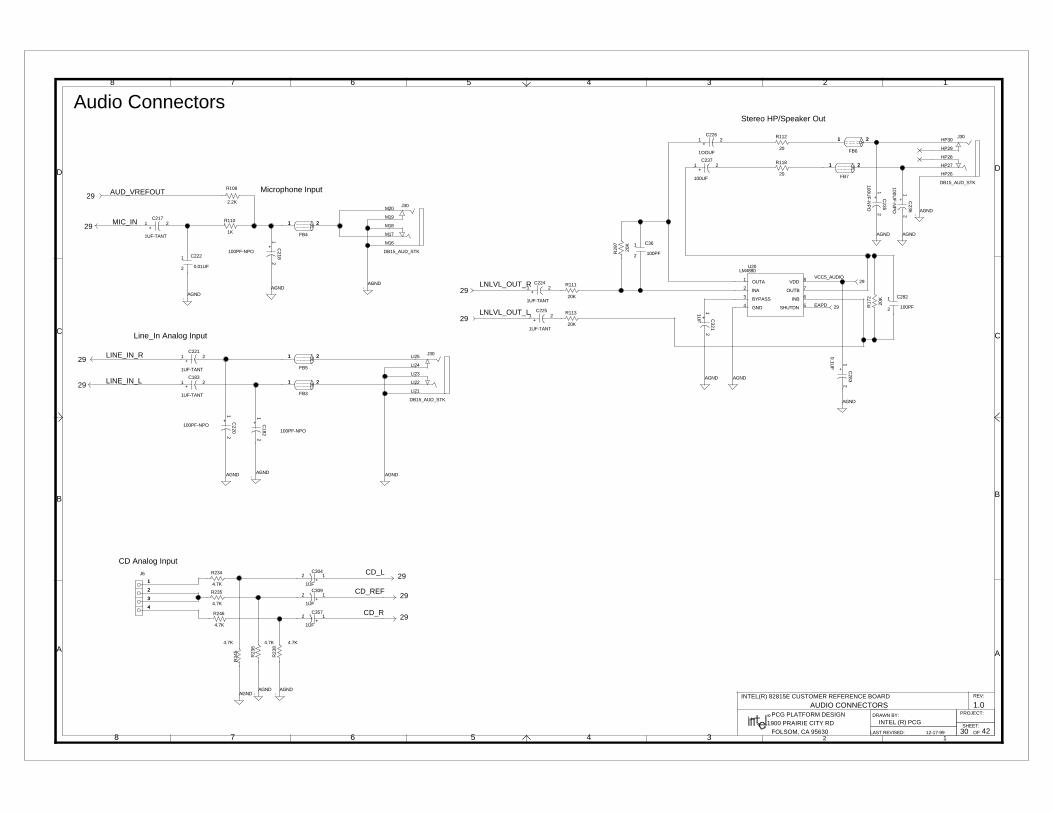
30
AUDIO CONNECTORS
100PF
C36
20K
R29
7
FB7
FB4
FB3
R118
20
2.2K
R108
29MIC_IN
29 AUD_VREFOUT
C221
1UF-TANT
29LINE_IN_R
29 LINE_IN_L
C218
100PF-NPO
C183
1UF-TANT
100PF-NPO
C220
J6
29CD_REF
29CD_R
4.7K
R235
4.7K
R246
4.7K
R24
5
4.7K
R23
6
1UF
C304
1UF
C309
1UF
C357
29CD_L
1UF-TANT
C217
R23
8
4.7K
29LNLVL_OUT_R
29LNLVL_OUT_L
R110
1K
1UF-TANT
C224
29EAPD 20K
R17
2
100PF
C282
29VCC5_AUDIO
1UF-TANT
C225
100UF
C237
C226
1OOUF
R112
20C
236
100UF
-NP
O
C235
100UF
-NP
O
100PF-NPO
C182
4.7K
R234
C222
0.01UF
FB5
FB6
C283
0.1UF
20K
R111
R113
20K
C321
1UF
U20
J30
J30
J30
1
2
21 21
21 21
211 2AGNDAGND
AGND
AGND AGND AGND
+1 2
+1
2
+21
+2
1
1
2
3
44
3
2
1 +12
+2 1
+2 1
+21
+1 2
2
1
+21
AGNDAGND
AGNDAGNDAGND
AGND
AGND
+1 2
+21
AGND
+1
2
+2
1
+1
2
1
2
21 21
211 2
AGND
+1
2
+2
1
LM4880
OUTA
INA
BYPASS
GND
VDD
OUTB
INB
SHUTDN 5
6
7
8
4
3
2
1
B
C
D
8 7 6 5 4 3 2 1
D
C
B
A
345678
A
2 1OFFOLSOM, CA 95630
1900 PRAIRIE CITY RD
PROJECT:
REV:
DRAWN BY:
SHEET:LAST REVISED:
PCG PLATFORM DESIGNINTEL (R) PCG
42
1.0INTEL(R) 82815E CUSTOMER REFERENCE BOARD
R
12-17-99
DB15_AUD_STK
LI22
LI23
LI24
LI25
LI21
DB15_AUD_STK
HP27
HP28
HP29
HP30
HP26
DB15_AUD_STK
M17
M18
M19
M20
M16
Stereo HP/Speaker Out
CD Analog Input
Microphone Input
Line_In Analog Input
Audio Connectors
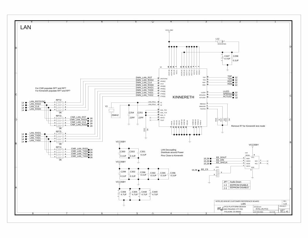
LAN
31
10K
R31
9
DWN_LAN_RST
C2960.1UF
C2650.1UF0.1UF
C260
C4484.7UF 4.7UF
C449
DWN_LAN_RXD2DWN_LAN_CLKDWN_LAN_RXD0DWN_LAN_RXD1DWN_LAN_TXD0DWN_LAN_TXD1DWN_LAN_TXD2
LAN_XTAL1
LAN_XTAL2
32LILEDSPEEDLED 32
RDN 3232RDP
TDN3232
TDP
EE_SHCLK15,2815,28 EE_DIN
LAN_TXD014 LAN_TXD114 LAN_TXD214
14 LAN_RXD1
0K
RP74
0K
RP75
28CNR_LAN_TXD2
CNR_LAN_TXD0 2828CNR_LAN_RXD1
28CNR_LAN_TXD1
28CNR_LAN_CLK
28CNR_LAN_RSTCNR_LAN_RXD2
28
28CNR_LAN_RXD0
U19
25MHZ
Y2
0.1UF
C300
22PF
C251
0.1UF
C301
0.1UF
C303
C302
0.1UF
0K
RP72
0K
RP73
LAN_RSTSYNC14
LAN_RXD014
LAN_CLK14
LAN_RXD214
C254
22PF
BLM11B750S
L12
4.7UFC447 C258
0.1UF
EE_DOUT15,28
U6
549
R31
6
R31
7
619
4.7UFC305C306
4.7UF
C2980.1UF
C299
0.1UF
JP25
15,28 EE_CS
32ACTLED
0K
R31
8
+1
2
+2
1
VCC3SBY
1
2
3
4 5
6
7
81
2
3
4 5
6
7
8
1
2
3
4 5
6
7
88
7
6
54
3
2
1
93C46
NC2 7
NC1 6
GND
5
EECS1EESK2EEDO4EEDI3 VCC
88
3
4
2
1
5
6
7
VCC3SBY
VCC3SBY
VCC3SBYB
C
D
8 7 6 5 4 3 2 1
D
C
B
A
345678
A
2 1OFFOLSOM, CA 95630
1900 PRAIRIE CITY RD
PROJECT:
REV:
DRAWN BY:
SHEET:LAST REVISED:
PCG PLATFORM DESIGNINTEL (R) PCG
42
1.0INTEL(R) 82815E CUSTOMER REFERENCE BOARD
R
12-17-99
1
2
3
4 5
6
7
81
2
3
4 5
6
7
8
1
2
3
4 5
6
7
88
7
6
54
3
2
1
1 2
VCC3_3SBY
+1
2
43 JTXD[0]44 JTXD[1]45 JTXD[2]
46 X1
29 ISOL_TEX30 ISOL_TCK28 ISOL_TI41 ADV1026 TOUT
47 X24RBIAS105RBIAS10021TESTEN
27LILED#31SPDLED#32
ACTLED#
16RDN
15RDP
11TDN
10TDP
7V
CC
A-7
2V
CC
A-2
9V
CC
T-9
12V
CC
T-1
2
14V
CC
T-1
4
17V
CC
T-1
7
1V
CC
-1
25V
CC
-25
42 JRSTSYNC37 JRXD[2]39
JCLK34 JRXD[0]35 JRXD[1]
3V
SS
A-3
6V
SS
A2-
6
18V
SS
-18
20V
SS
R-2
0
22V
SS
R-2
2
38V
SS
P-3
8
24V
SS
-24
8V
SS
-8
48V
SS
-48
13V
SS
-13
33V
SS
P-3
319
VC
CR
-19
23V
CC
R-2
3
36V
CC
P-3
6
40V
CC
P-4
0
KINNERETH
40 36 23 19
3313 488 24 38 22 2018 6 3
35
34
39
37
42
25 1 17 14 12 9 27
10
11
15
16
32
31
27
21
5
447
26
41
28
30
29
46
45
44
43
+1
2
+2
1
1
2
33
2
1
Audio Down
1-2
2-3
Remove R? for Kinnereth test mode
LAN
Distribute around Power
Pins Close to Kinnereth
JP?
LAN Decoupling
For Kinnereth populate RP? and RP?For CNR populate RP? and RP?
EEPROM ENABLEEEPROM DISABLE

LAN
32
J2
31,32SPEEDLED
R146330 330
R147
JP15JP14
31,32 LILED
AC
T_C
R
31,32 SPEEDLED
JP7_
PU
JP16
330R148
JP18
_PU
JP23
_PU
LI_CR
330R138
ACTLED31,32
R23
330ACTLED 31,32
31,32LILED
100R294
121R295
31RDN
TDN3131 RDP
TDP31
21C
AS
E0
CA
SE
122 23
CA
SE
224
CA
SE
3C
AS
E4
25
CA
SE
526
CA
SE
627
10
12
9
11NC18
P1919P20
20
16 RD+
RD-17
15 RDC
TD-14
RJMAG/USB13 TD+
CA
SE
728
14
13
15
17
16
20
19
18
11
9
12
10
2827262524232221
VCC3SBY
VCC3SBY
B
C
D
8 7 6 5 4 3 2 1
D
C
B
A
345678
A
2 1OFFOLSOM, CA 95630
1900 PRAIRIE CITY RD
PROJECT:
REV:
DRAWN BY:
SHEET:LAST REVISED:
PCG PLATFORM DESIGNINTEL (R) PCG
42
1.0INTEL(R) 82815E CUSTOMER REFERENCE BOARD
R
12-17-99
Note: Chassis Ground,use plane for this signal
LAN
No Pop R295
Place R294 and R295 near Kennereth
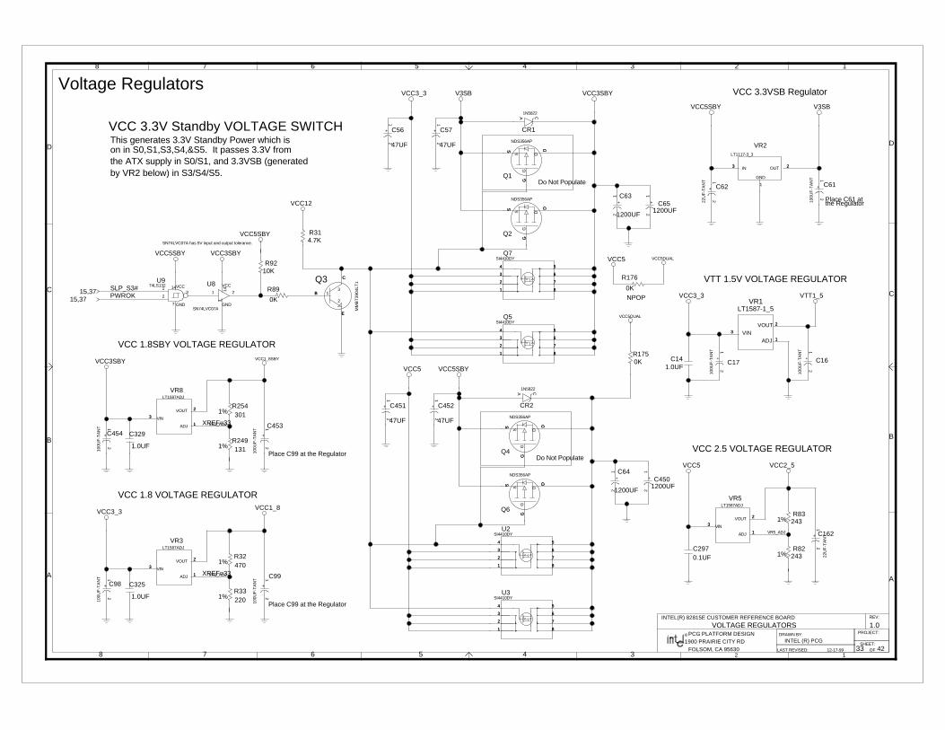
VOLTAGE REGULATORS
33
1%R249131
XREF=33VR1_ADJ C453
100U
F-T
AN
T
C454
100U
F-T
AN
T
VR8
301R254
1%
R176
0K
C4501200UF
Q6
Q4
C451
47UF
C452
47UF
U3
U2
CR2
1N5822
1200UF
C64
1200UF
C63
R822431%
243R83
1%
470R32
1%
15,37 SLP_S3#
15,37 PWROK
4.7KR31
MM
BT
3904
LT1Q3
VR5
CR1
1N5822
0.1UFC297
Q7
Q5
C141.0UF
1.0UF
C325
C62
22U
F-T
AN
T
100U
F-T
AN
T
C61
C98
100U
F-T
AN
T C99
100U
F-T
AN
T
22U
F-T
AN
TC162
100U
F-T
AN
T
C17
100U
F-T
AN
T
C16
C57
47UF
C56
47UF
XREF=33VR1_ADJ
VR5_ADJ
U8
Q1
Q2
1%R33220
U9
C651200UF
LT1587-1_5VR1
VR2
R89
0K
R9210K
0KR175
1.0UF
C329
VR3
VCC3SBY
+1
2
+1
2
VIN3
2VOUT
1ADJ
LT1587ADJ
3
2
1
+2
1
NDS356AP
GG
D
D
S
S
S D
G
NDS356AP
GG
D
D
S
S
G
DS
+1
2
+2
1
SI4410DY
8
7
6
54
3
2
11
2
3
4
8
7
6
5
SI4410DY
8
7
6
54
3
2
1
5
6
7
8
4
3
2
1
A C
+2
1+
12
V3SB
VTT1_5VCC3_3
VCC2_5
VCC5SBY
VCC3SBY
B 13
C
2
EE
C
B
VCC12
VCC1_8
VCC5SBY
VCC3_3
V3SB
VCC3_3
VIN3
2VOUT
1ADJ
LT1587ADJ
2
3
1
CA
SI4410DY
8
7
6
54
3
2
11
2
3
4
8
7
6
5
SI4410DY
8
7
6
54
3
2
1
5
6
7
8
4
3
2
1
+2
1
+2
1
+2
1
+2
1
+2
1
+2
1
+2
1
+1
2
+2
1
SN74LVC07AGND
VCC
14
7
1 2
NDS356AP
GG
D
D
S
S
S D
G
NDS356AP
GG
D
D
S
S
G
DS
74LS132 VCC
GND7
143
2
1
+1
2
VIN3
2VOUT
1ADJ 1
2
3
1
GND
IN3 OUT 2
LT1117-3_3
3 2
VCC5
VCC5SBY
VCC5SBY
VCC5 VCC5DUAL
VCC5DUAL
VCC5
B
C
D
8 7 6 5 4 3 2 1
D
C
B
A
345678
A
2 1OFFOLSOM, CA 95630
1900 PRAIRIE CITY RD
PROJECT:
REV:
DRAWN BY:
SHEET:LAST REVISED:
PCG PLATFORM DESIGNINTEL (R) PCG
42
1.0INTEL(R) 82815E CUSTOMER REFERENCE BOARD
R
12-17-99
VCC3SBY
VCC1_8SBY
VIN3
2VOUT
1ADJ
LT1587ADJ
1
2
3
Place C99 at the RegulatorDo Not Populate
VCC 2.5 VOLTAGE REGULATOR
VTT 1.5V VOLTAGE REGULATOR
the Regulator
VCC 1.8 VOLTAGE REGULATOR
Do Not Populate
VCC 3.3VSB Regulator
VCC 3.3V Standby VOLTAGE SWITCHThis generates 3.3V Standby Power which ison in S0,S1,S3,S4,&S5. It passes 3.3V fromthe ATX supply in S0/S1, and 3.3VSB (generatedby VR2 below) in S3/S4/S5.
SN74LVC07A has 5V input and output tolerance.
Voltage Regulators
Place C61 at
NPOP
Place C99 at the Regulator
VCC 1.8SBY VOLTAGE REGULATOR

34
AGP VOLTAGE REGULATOR
Q13
1K
R20
9
1
2
VDDQ_FB
VDDQ_G VDDQ_G2
VDDQ_COMP
10 TYPEDET#VR_SDB
1KR21
1
2
1
10K
R20812
2.2K
R12
1
1
2
R21
0
0K
2
1
C31
6
1UF
1
2
10U
F
C31
5
2
1
220UF
C317
1 2
0.001UF
C26812
R156
7.5K-1%
1 2
R155
5.1-5%21
301
R16
2 1%
2
1
1.21
K-1
%
R16
1
1
2
R17
4
1K
1
2
VR_SHUTDOWN
C267
10PF2 1
LT1575VR6
8
7
6
5
1
2
3
4
C32
2
47U
F
1
2
C27
8
22U
F
2
1
C24
2
1UF
-X7R
2
1
C27
0
1UF
-X7R
1
2
1UF
-X7R
C26
9
2
1
C27
1
1UF
-X7R
1
2
MM
BT
3904
LT1Q14
MM
BT
3904
LT1
Q15
1 1
IRL2
203N
S
2
2
3
3
3
2
1
VCC12
VCC3_3
+
+
+
+VCC1_8
VCC3_3
IPOS
INEG
GATE
COMP
SHDN
VIN
GND
FB
+
VDDQ
+++++
B 13
C
2
E
B
C
E
B 13
C
2
EE
C
B
B
C
D
8 7 6 5 4 3 2 1
D
C
B
A
345678
A
2 1OFFOLSOM, CA 95630
1900 PRAIRIE CITY RD
PROJECT:
REV:
DRAWN BY:
SHEET:LAST REVISED:
PCG PLATFORM DESIGNINTEL (R) PCG
42
1.0INTEL(R) 82815E CUSTOMER REFERENCE BOARD
R
12-17-99
AGP Voltage Regulator
Route VR6 GND to VDDQ output caps and then via to ground.
No stuff R210

VRM 8.4
35
PV
12
R_VID2R_VID1R_VID0
C25
2200
UF
Q8
Q11
C455
2200
UF
2200
UF
C72
R53
20
220
R93
OUTEN
JP4JP5 JP6 JP3
5.6K
R26
0.1UFC46
150PF
C70
10K
R34
1000PF
C69
Q12
Q9
2200
UF
C28C126
2200
UF
0.1UF
C71
1200UF
C117
1200UF
C78C66
0.1UF 10UF
C169
C113
1.0U
F-X
7R
FAULT#_PU
VRM_PWRGD15
G1
G2
L_VCCVIDR_VCCVID
VFB_PD
SS_PDVRCOMP_PD
R_V
RC
OM
P R35
8.2K
0.01UF
C31
VR4
3 VID[3:0]
VID0VID1VID2VID3
R375.1
C27
1.0UF
0.01UF
C74 R36
2.7K
IMAX
R_VID3
RP7
0K ETQP6F0R8L
L13
1.0UH-20A
C1141.0UF-X7R
DO3316P-102L9
1.0U
H
1200UF
C76
5VIN
C115
1200UF
+1
2
G1
4
S1
1
S2
2
S3
3
D1
8
D2
7
D3
6
D4
5
SI4410D
Y
4 123
8765G
14
S1
1
S2
2
S3
3
D1
8
D2
7
D3
6
D4
5
SI4410D
Y
5 6 7 8
3 2 14
+1
2
+1
2
VCC3_3
VCCVID
VCC5
G1
4
S1
1
S2
2
S3
3
D1
8
D2
7
D3
6
D4
5
SI4410D
Y
4 123
8765G
14
S1
1
S2
2
S3
3
D1
8
D2
7
D3
6
D4
5
SI4410D
Y
5 6 7 8
3 2 14
+1
2
+2
1
VCC5
+2
1
+1
2
+2
1
LTC1753 6S
EN
SE
9S
S
4S
GN
D
3G
ND
VC
C5
PV
CC
2
CO
MP
10
VID414VID315VID216VID117VID018OUTEN19 IMAX 7
13PWRGD
FAULT# 12
G1 20
G2 1
8IFB
11VFB 11
8
1
20
12
13
719
18
17
16
15
14
10
25
349 6
VCC12
1
2
3
4 5
6
7
88
7
6
54
3
2
1
+1
2
+1
2
B
C
D
8 7 6 5 4 3 2 1
D
C
B
A
345678
A
2 1OFFOLSOM, CA 95630
1900 PRAIRIE CITY RD
PROJECT:
REV:
DRAWN BY:
SHEET:LAST REVISED:
PCG PLATFORM DESIGNINTEL (R) PCG
42
1.0INTEL(R) 82815E CUSTOMER REFERENCE BOARD
R
12-17-99
Sanyo 4SP2200M
Place caps next to output FETs.
VID Override Jumpers
Close to FETsPlace CAPs
If your VR IC does not incorporate these, they mustThe LTC1753 incorporates internal pull-ups on VID[4:0].
go on the motherboard.
Refer to VR Supplier for Layout Guidelines
Processor Voltage Regulator
Do Not Stuff
C76,C115,C78,C117 must support >8A of RMS current.
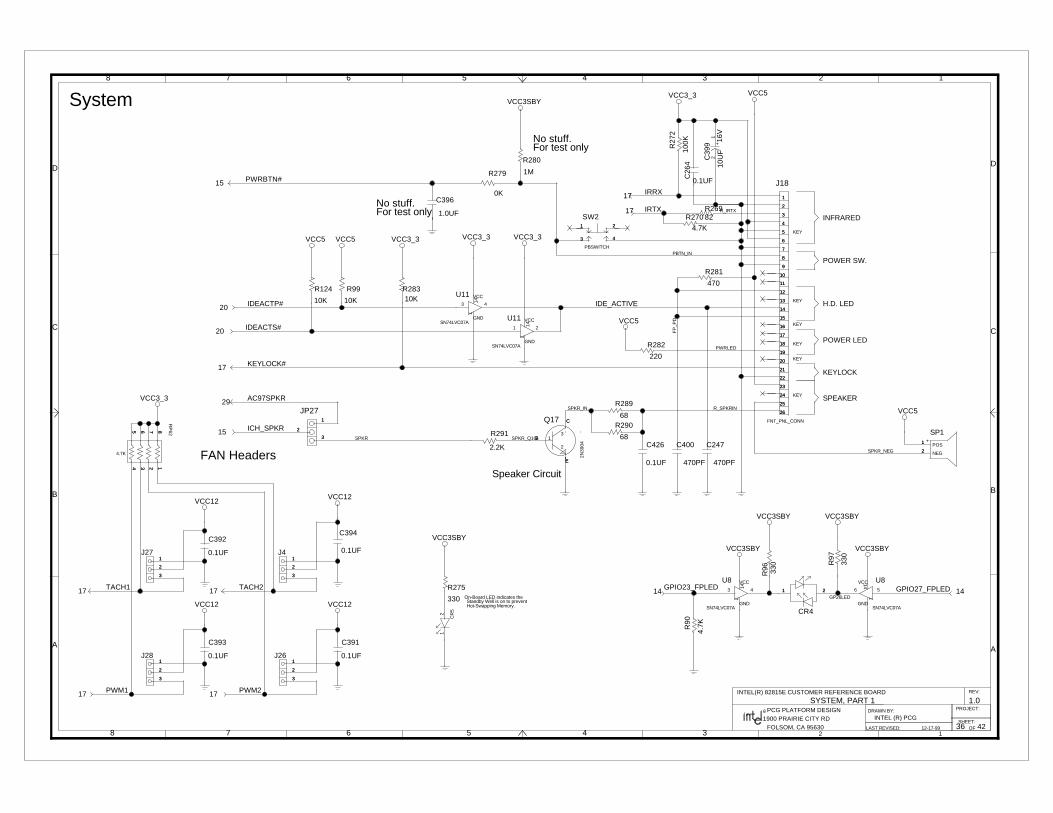
SYSTEM, PART 1
36
17 PWM1
17 TACH1
17 PWM2
17 TACH2
R90
4.7K
330
R275
2.2K
R291
10K
R99
10K
R124
R281
470
R279
0K
1M
R280
R282
220
68
R289
C426
0.1UF
KEYLOCK#17
J26J28
J4
Q17JP27
15 ICH_SPKR SP1
J18
29 AC97SPKR
J27
82R269
4.7K
R270IRTX17
IRRX17
20 IDEACTP#U11
15 PWRBTN#
U11
20 IDEACTS#
IDE_ACTIVE
68
R290
C39
9
10U
F16
V
10KR283
0.1UF
C394
C247
470PF
0.1UF
C391
0.1UF
C392
0.1UF
C393
U8U8
14GPIO27_FPLED
R27
2
100K
R96 33
0
14 GPIO23_FPLED
330
R97
CR4
C26
4
0.1UF
C396
1.0UF
C400
470PF
SPKR_NEG
R_SPKRIN
SPKR
SPKR_IN
SPKR_Q1G
FP
_PD
R_IRTX
PWRLED
GP26LED
PBTN_IN
SW2
4.7K
RP
62
CR
5
VCC3SBY
1
2
33
2
11
2
3
1
2
3
1
2
3
1
2
32N
3904
B 13
C
2
EE
C
B
VCC51
2
33
2
1
2 NEG
1 POS+1
2
FNT_PNL_CONN
1
10
11
12
13
14
15
16
17
18
19
2
20
21
22
23
24
25
26
3
4
5
6
7
8
9
26
25
24
23
22
21
20
19
18
17
16
15
14
13
12
11
10
9
8
7
6
5
4
3
2
1
VCC12VCC12
VCC12VCC12
VCC3_3
1
2
33
2
1
VCC3_3
SN74LVC07AGND
VCC
3
7
414
SN74LVC07AGND
VCC
14 2
7
1
VCC5
VCC5
+2
1
VCC5 VCC5 VCC3_3 VCC3_3 VCC3_3
SN74LVC07AGND
VCC
5
7
6
14
SN74LVC07AGND
VCC
14 4
7
3
VCC3SBY VCC3SBY
VCC3SBY VCC3SBY
211 2
PBSWITCH
1 2
3 443
21
12345 6 7 88765
4 3 2 1
VCC3SBY
B
C
D
8 7 6 5 4 3 2 1
D
C
B
A
345678
A
2 1OFFOLSOM, CA 95630
1900 PRAIRIE CITY RD
PROJECT:
REV:
DRAWN BY:
SHEET:LAST REVISED:
PCG PLATFORM DESIGNINTEL (R) PCG
42
1.0INTEL(R) 82815E CUSTOMER REFERENCE BOARD
R
12-17-99
21
Standby Well is on to preventOn-Board LED indicates the
KEY
KEY
KEY
KEY
KEY SPEAKER
KEYLOCK
H.D. LED
POWER SW.
INFRARED
Speaker Circuit
FAN Headers
No stuff.For test only
No stuff.For test only
POWER LEDKEY
Hot-Swapping Memory.
System
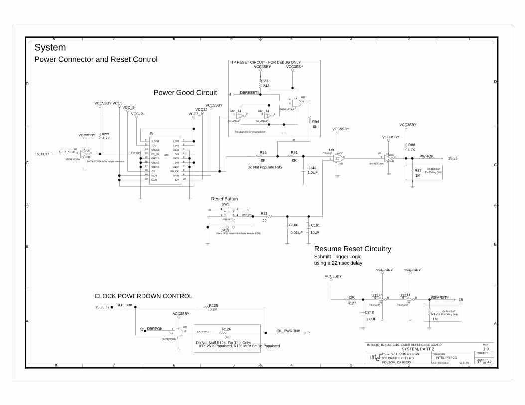
SYSTEM, PART 2
37
37
RST_PD
R1258.2K
C1481.0UF
1MR128
R127
22K
1MR87
R884.7K
C160
0.01UF
22
R81
R224.7K
R940K
243R123
15RSMRST#U12
U7
U7
U12
4 DBRESET#
U12
U12
10UF
C161
5VPSON
J5
C248
1.0UF
SLP_S3#15,33,37 R91
0K
CK_PWRDN# 637 DBRPOK
PWROK 15,33
R126
0K
CK_PWRD
SW1
JP13
SLP_S3#15,33,37
U10
U9
U10
0K
R95
74LVC14A
14
7
89
SN74LVC06AGND
VCC65
14
7
VCC3SBY
SN74LVC06AGND
VCC43
14
7
VCC5SBY
VCC3SBY
VCC3_3
VCC_5-
VCC3SBY
VCC3SBY VCC3SBY
VCC5SBYVCC5
VCC5SBY
74LVC14A
14
7
21
VCC3SBY
74LVC14A
14
7
65
74LVC14A
3 4
7
14
VCC3SBY
+2
1
VCC12-VCC12
ATX
3_3V11
-12V
GND13
PS_0N
GND15
GND16
GND17
-5V
5V19
5V20
3_3V1
3_3V2
GND3
5V4
GND5
5V6
GND7
PW_OK
5VSB
12V 10
9
8
7
6
5
4
3
2
1
20
19
18
17
16
15
14
13
12
11
VCC3SBY
VCC3SBY
PBSWITCH
1 2
3 443
21
SN74LVC08A7
5
46
14
74LS132 VCC
GND7
146
5
4
SN74LVC08A7
148
9
10
B
C
D
8 7 6 5 4 3 2 1
D
C
B
A
345678
A
2 1OFFOLSOM, CA 95630
1900 PRAIRIE CITY RD
PROJECT:
REV:
DRAWN BY:
SHEET:LAST REVISED:
PCG PLATFORM DESIGNINTEL (R) PCG
42
1.0INTEL(R) 82815E CUSTOMER REFERENCE BOARD
R
12-17-99
Do Not Populate R95
Power Good Circuit
ITP RESET CIRCUIT - FOR DEBUG ONLY
74LVC14A is 5V input tolerant
SN74LVC06A is 5V output tolerance
CLOCK POWERDOWN CONTROL
Reset Button
Do Not StuffFor Debug Only
Resume Reset CircuitrySchmitt Trigger Logicusing a 22msec delay
For Debug OnlyDo Not Stuff
SystemPower Connector and Reset Control
Place JP13 Near Front Panel Header (J20)
If R125 is Populated, R126 Must Be De-PopulatedDo Not Stuff R126- For Test Only:

PULLUP/PULLDOWN RESISTORS
38
VC
MO
S
4,14,15
LPC_PME#15,17GPIO2114,19
SERIRQ14,17,19
11,12,13,14,15,27,28 SMBCLK11,12,13,14,15,27,28 SMBDATA
2.7K
RP76
10,14,18,19 PIRQ#A10,14,18,19 PIRQ#B
1%110
R12
PCPCI_REQ#A14,19
U11
U11
R263
10K R262
10K
IRQ1514,2014,20 IRQ14
150
R11
PU2_ACK64#18PU2_REQ64#18
4 SLEWCTRL
4 RTTCTRL
18 SDONEP2
18 SBOP2
PTMS18,19
PTDI18,1919 SBOP3
14,18,19 SERR#
14,18,19 PLOCK#
14,18,19 STOP#
14,18,19 DEVSEL#
14,18,19 TRDY#
14,18,19 IRDY#
PIRQ#D14,18,1914,18,19 PIRQ#C
14,18,19 PERR#
14,19 PREQ#2
14,18 PREQ#1
14 PGNT#3
14,18 PGNT#0
14,18 PGNT#1
14,19 PGNT#2
14 PREQ#3
14,18,19 FRAME#
4,14 APICD0
4,14 APICD1
2.7K
RP67
RP66
2.7K
RP57
5.6K
5.6K
RP58
150
R13
RP52
8.2K
15,28,29 AC_SDIN0
15,28 AC_SDIN1
U12
U12
U7U9
U9
U8
U8
RP53
8.2KRP54
8.2K
RP51
8.2K
RP61
4.7K
14,17 A20GATE
4,14 FERR#
15,17 LPC_SMI#
14,17 RCIN#
15 SMBALERT#LDRQ#115
THERM#14,15
150
R14
1%110
R28
U11
PU3_REQ64#19
PU3_ACK64#19PREQ#014,18
19 SDONEP3
2.7K
RP59
U8
VCC3_3
1
2
3
4 5
6
7
88
7
6
54
3
2
1
VCC5SBY
VCC3_3
SN74LVC07AGND
VCC
13
7
1214
SN74LVC07AGND
VCC
14 10
7
11
VCC3SBY
VCC5
VCC5
RESISTOR PAK9 PULLUP/DOWN
1
10
3
2
9
8
7
6
5
4
RESISTOR PAK9 PULLUP/DOWN
1
10
3
2
9
8
7
6
5
4
1
2
3
4 5
6
7
81
2
3
4 5
6
7
8
1
2
3
4 5
6
7
88
7
6
54
3
2
1
VCC5
VCC5
VCC5
1
2
3
4 5
6
7
88
7
6
54
3
2
1
74LVC14A
14
7
1011
74LVC14A
13 12
7
14
SN74LVC06AGND
VCC
7
1413 12
74LS132 VCC
GND
12
1311
14
7
74LS132 VCC
GND7
148
10
9
VCC3SBY
SN74LVC07AGND
VCC
14 8
7
9
SN74LVC07AGND
VCC
11
7
1014
1
2
3
4 5
6
7
81
2
3
4 5
6
7
8
1
2
3
4 5
6
7
88
7
6
54
3
2
1
1
2
3
4 5
6
7
81
2
3
4 5
6
7
8
1
2
3
4 5
6
7
81
2
3
4 5
6
7
8
VCC3SBY
SN74LVC07AGND
VCC
9
7
814
B
C
D
8 7 6 5 4 3 2 1
D
C
B
A
345678
A
2 1OFFOLSOM, CA 95630
1900 PRAIRIE CITY RD
PROJECT:
REV:
DRAWN BY:
SHEET:LAST REVISED:
PCG PLATFORM DESIGNINTEL (R) PCG
42
1.0INTEL(R) 82815E CUSTOMER REFERENCE BOARD
R
12-17-99
1
2
3
4 5
6
7
81
2
3
4 5
6
7
8
VCC3_3
VCC3_3
VCC3_3
VCC3SBY
SN74LVC07AGND
VCC
14 12
7
13
For Future Compatibility Upgrade
Pull-up Resistors and unused gates
UNUSED GATES
CPUICH
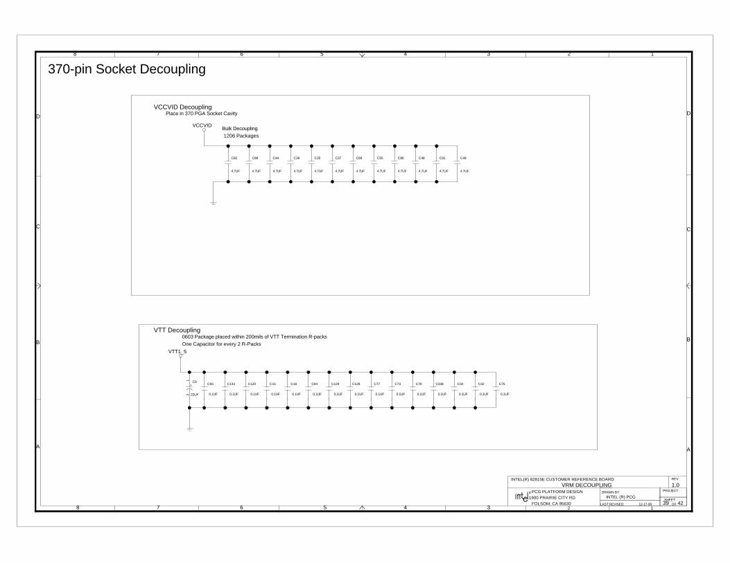
VRM DECOUPLING
39
4.7UF
C86
22UF
C6
0.1UF
C93 C134
0.1UF 0.1UF
C120 C15
0.1UF
C18
0.1UF
C94
0.1UF 0.1UF
C129 C128
0.1UF 0.1UF
C77
0.1UF
C73
0.1UF
C79 C338
0.1UF 0.1UF
C34 C32
0.1UF
C82
4.7UF 4.7UF
C88 C44
4.7UF 4.7UF
C39 C35
4.7UF 4.7UF
C37 C89
4.7UF 4.7UF
C55
4.7UF
C48 C91
4.7UF
C49
4.7UF
C75
0.1UF
+2
1
VTT1_5
VCCVID
B
C
D
8 7 6 5 4 3 2 1
D
C
B
A
345678
A
2 1OFFOLSOM, CA 95630
1900 PRAIRIE CITY RD
PROJECT:
REV:
DRAWN BY:
SHEET:LAST REVISED:
PCG PLATFORM DESIGNINTEL (R) PCG
42
1.0INTEL(R) 82815E CUSTOMER REFERENCE BOARD
R
12-17-99
VCCVID Decoupling
VTT Decoupling
Place in 370 PGA Socket Cavity
370-pin Socket Decoupling
0603 Package placed within 200mils of VTT Termination R-packsOne Capacitor for every 2 R-Packs
Bulk Decoupling1206 Packages
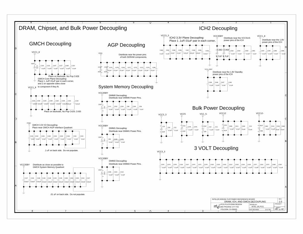
40
DRAM, ICH, AND GMCH DECOUPLING
C437
0.1UF0.1UF
C438
0.1UF
C439 C440
0.1UF
22UF
C457
0.1UF
C415C436
0.1UF
C368
0.1UF0.1UF
C363C342
0.1UF
C456
4.7UF0.01UF
C324
0.1UF
C433
0.1UF
C431C432
0.1UF
0.01UF
C427
0.01UF
C434C435
0.01UF0.01UF
C201C200
0.01UF0.01UF
C138C133
0.01UF0.01UF
C199
0.01UF
C139
0.01UF
C137
0.01UF
C132
0.01UF
C191
C314
0.1UF0.1UF
C418
0.1UF
C318 C377
0.1UF 0.1UF
C369C372
0.1UF 0.1UF
C320
0.1UF
C313
0.1UF
C420C374
0.1UF 0.1UF
C371C417
0.1UF0.1UF
C376
C362
0.1UF
C21
0.1UF
C378
0.1UF
22UF
C20
C428
0.1UF0.1UF
C127
0.1UF
C197C131
0.1UF0.1UF
C193
0.1UF
C441
0.1UF
C142C95
0.1UF
C58
0.1UF
C246
0.1UF0.1UF
C96C204
0.1UF
0.1UF
C274C272
0.1UF0.1UF
C273
0.1UF
C277C243
0.1UF
0.01UF
C328
0.1UF
C232C228
0.1UF0.1UF
C234
C430
0.01UF
C429
0.01UF 0.01UF
C339
0.01UF
C240
0.01UF
C223
0.01UF
C194
0.01UF
C326
0.1UF
C287
0.1UF
C292
22UF
C97
C141
0.1UF 0.1UF
C202
C229
0.1UF
0.1UF
C22 C365
0.1UF
0.1UF
C275 C276
0.1UF
0.1UF
C23C59
0.1UF
0.1UF
C375 C373
0.1UF 0.1UF
C416 C370
0.1UF 0.1UF
C319 C419
0.1UF 0.1UF
C323
10UF
C192 C238
10UF
C288
10UF
C383
0.1UF 0.1UF
C332 C290
0.1UF 0.1UF
C293 C327
0.01UF
0.1UF
C379
22UF
C421C24
22UF
C241
22UF
22UF
C60
22UF
C366
C364
0.1UF0.1UF
C413 C310
0.1UF0.1UF
C311
0.1UF
C349
0.1UF
C19
0.1UF
C231
C136
0.01UF 0.01UF
C198
0.1UF
C230
C135
0.1UF
C382
4.7UF0.1UF
C381
0.1UF
C343 C286
0.1UF
0.1UF
C414
C281
0.1UF
+1
2
VCC3SBY
+1
2
VDDQ
VCC3SBY
VCC3_3
VCC3_3
VCC3SBYVCC3_3
VCC1_8
VCC3SBY
+1
2
VCC1_8
+2
1
VCC5 VCC_5-
+1
2
+2
1
+1
2
+2
1
+2
1
+1
2+1
2
+2
1
VCC12-VCC12
VCC3SBY
VCC1_8
VDDQ
B
C
D
8 7 6 5 4 3 2 1
D
C
B
A
345678
A
2 1OFFOLSOM, CA 95630
1900 PRAIRIE CITY RD
PROJECT:
REV:
DRAWN BY:
SHEET:LAST REVISED:
PCG PLATFORM DESIGNINTEL (R) PCG
42
1.0INTEL(R) 82815E CUSTOMER REFERENCE BOARD
R
12-17-99
+2
1
VCC1_8SBY
power pins of the ICH
GMCH Decoupling
of both SDRAM components.Distribute near the power pins
DRAM, Chipset, and Bulk Power Decoupling
GMCH 3.3V IO Decoupling:
DIMM1 Decoupling:
DIMM0 Decoupling:Distribute near DIMM0 Power Pins.
Distribute near DIMM1 Power Pins.
Place 1 .1uF/.01uF pair in each corner,and 2 on opposite sides close
to component if they fit.
GMCH System Memory QuadrantDistribute as close as possible to
GMCH Core Plane Decoupling:
Place on backside, No Pop C429, C430
Place on backside, No Pop C428
Distribute near the VCCSUSpower pins of the ICHPlace 1 .1uF/.01uF pair in each corner,
ICH2 3.3V Plane Decoupling:
Place near GMCH AGP interface Quadrant
DIMM2 Decoupling:Distribute near DIMM2 Power Pins.
.1 uF on back side. Do not populate.
.01 uF on back side. Do not populate.
3 VOLT Decoupling
System Memory Decoupling
AGP Decoupling
ICH2 Decoupling
Bulk Power Decoupling
power pins of the ICHDistribute near the 1.8V
Distribute near the 1.8V Standby
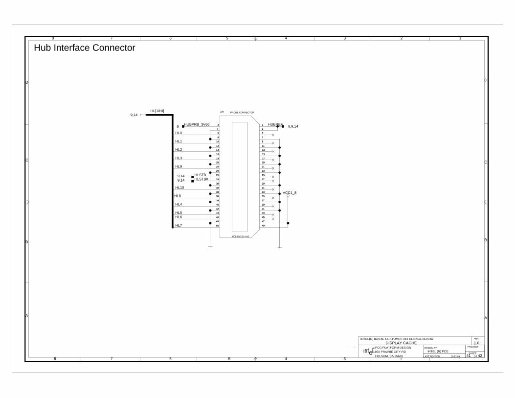
DISPLAY CACHE
41
HL9
HL7
HL6HL5
HL4
HL8
HL10
HL3
HL2
HL0
HL1
9,14HL[10:0] J29
8,9,14HUBREFHUBPRB_3V666
9,14 HLSTB
9,14 HLSTB#
1
19
21
23
25
31
33
35
37
3
39
41
43
45
47
49
5
7
9
13
15
17
20
22
24
26
28
30
32
34
36
38
40
42
44
46
6
8
10
12
14
16
18
2
4
48
50
11
29
27
P08-050-SL-A-G
PROBE CONNECTOR
27
29
11
50
48
4
2
18
16
14
12
10
8
6
46
44
42
40
38
36
34
32
30
28
26
24
22
20
17
15
13
9
7
5
49
47
45
43
41
39
3
37
35
33
31
25
23
21
19
1
VCC1_8
B
C
D
8 7 6 5 4 3 2 1
D
C
B
A
345678
A
2 1OFFOLSOM, CA 95630
1900 PRAIRIE CITY RD
PROJECT:
REV:
DRAWN BY:
SHEET:LAST REVISED:
PCG PLATFORM DESIGNINTEL (R) PCG
42
1.0INTEL(R) 82815E CUSTOMER REFERENCE BOARD
R
12-17-99
Hub Interface Connector
42
REVISION HISTORY
B
C
D
8 7 6 5 4 3 2 1
D
C
B
A
345678
A
2 1OFFOLSOM, CA 95630
1900 PRAIRIE CITY RD
PROJECT:
REV:
DRAWN BY:
SHEET:LAST REVISED:
PCG PLATFORM DESIGNINTEL (R) PCG
42
1.0INTEL(R) 82815E CUSTOMER REFERENCE BOARD
R
12-17-99
Revision History
- Initial release revision 1.0


