– Read-Only Memory (ROM): Programmed at manufacture
• Being phased out of use in favor of Flash
– Read-Write Memory: Can change value dynamically
• SRAM, DRAM
– Read-Mostly: Can write, but much more slowly than read
• EEPROM (Electrically Eraseable, Programable Read Only Memory) (pronounced “Double E Prom”)
• Flash (A form of EEPROM)
Volatility: sensitivity to losing power
– Volatile: loses contents when power turned off
– Non-volatile: does not lose contents
Semiconductor Memory Slide 4
3
CMOS VLSI Design
Memory Characteristics Addressability
– Random-Access: provide address to access a “word” of data
• No correlation between successive addresses
– Block oriented: read and write large blocks of data at a time
– Content-addressable: search memory for match against partial data
– Serial Access: e.g.. FIFO. Queue, stack
Wearout
– Some memories have a limited number of write cycles before changing characteristics renders them unusable
Cell Size
– Primary determinent of the physical size of the memory array
Semiconductor Memory Slide 5
CMOS VLSI Design
Lecture Focus The most used technologies
– SRAM
• Local memory
• Registers, Cache
– DRAM
• Main memory for computers and processors
– Flash and other EEPROMs
• Program and data storage
• Operational parameter storage– Used in controllers for everything from a key fob to
an automobile engine/transmission.
Semiconductor Memory Slide 6
4
CMOS VLSI Design
Memory Features
Note: Flash is process compatible with SRAM but DRAM is not.
Semiconductor Memory Slide 7
SRAM DRAM Flash
Non‐volitile No No YesCell Size (F^2) 25 to 40 6 to 8 4 to 5
Read Access Time ~ 0.1 ns ~ 10 ns ~ 10 nsWrite Time ~ 0.1 ns ~ 10 ns N.A.Erase Time N.A. N.A. ~ 10 ms
Program Time N.A. N.A. ~ 10 usWearout N.A. N.A. 10k to 100k
erase/program cycles
Use in Computer/Processor
Systems
RegistersCache
(L1, L2, L3)
Main Memory Program and Data Storage
CMOS VLSI Design
Generic Memory Architecture
Westre and Harris, Chapter 12
Semiconductor Memory Slide 8
5
CMOS VLSI Design
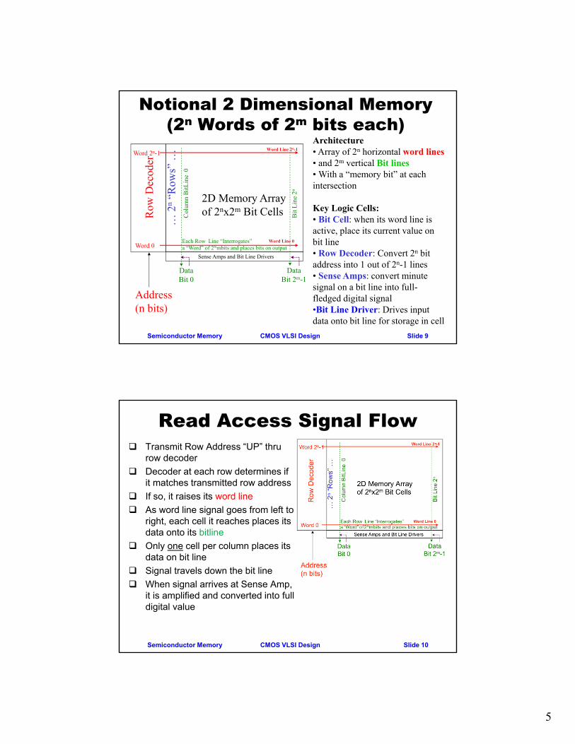
Notional 2 Dimensional Memory (2n Words of 2m bits each)
Architecture• Array of 2n horizontal word lines• and 2m vertical Bit lines• With a “memory bit” at each intersection
Key Logic Cells:• Bit Cell: when its word line is active, place its current value on bit line • Row Decoder: Convert 2n bit address into 1 out of 2n-1 lines• Sense Amps: convert minute signal on a bit line into full-fledged digital signal•Bit Line Driver: Drives input data onto bit line for storage in cell
Semiconductor Memory Slide 9
DataBit 2m-1
2D Memory Arrayof 2nx2m Bit CellsR
ow D
ecod
er
Address(n bits)
… 2
n“R
ows”
…
Each Row Line “Interrogates”a “Word” of 2Nmbits and places bits on output
DataBit 0
Word 0
Word 2n-1
Col
umn
Bit
Lin
e 0
Bit
Lin
e 2n
Sense Amps and Bit Line Drivers
Word Line 0
Word Line 2n-1
CMOS VLSI Design
Read Access Signal Flow Transmit Row Address “UP” thru
row decoder
Decoder at each row determines if it matches transmitted row address
If so, it raises its word line
As word line signal goes from left to right, each cell it reaches places its data onto its bitline
Only one cell per column places its data on bit line
Signal travels down the bit line
When signal arrives at Sense Amp, it is amplified and converted into full digital value
Semiconductor Memory Slide 10
6
CMOS VLSI Design
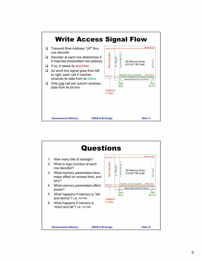
Write Access Signal Flow Transmit Row Address “UP” thru
row decoder
Decoder at each row determines if it matches transmitted row address
If so, it raises its word line
As word line signal goes from left to right, each cell it reaches receives its data from its bitline
Only one cell per column receives data from its bit line
Semiconductor Memory Slide 11
CMOS VLSI Design
1. How many bits of storage?
2. What is logic function at each row decoder?
3. What memory parameters have major effect on access time, and why?
4. What memory parameters affect power?
5. What happens if memory is “tall and skinny”? i.e. n>>m
6. What happens if memory is “short and fat”? i.e. n<<m
Questions
Semiconductor Memory Slide 12
7
CMOS VLSI Design
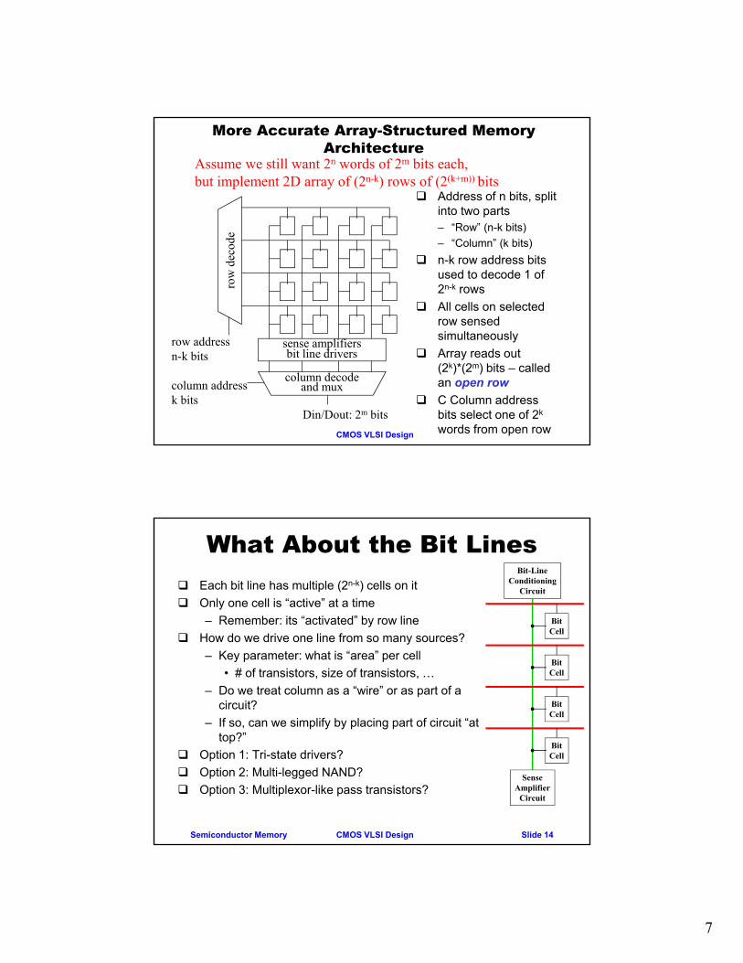
More Accurate Array-Structured Memory Architecture
column decodeand mux
sense amplifiersbit line drivers
row
dec
ode
row addressn-k bits
column addressk bits
Din/Dout: 2m bits
Address of n bits, split into two parts– “Row” (n-k bits)
– “Column” (k bits)
n-k row address bits used to decode 1 of 2n-k rows
All cells on selected row sensed simultaneously
Array reads out (2k)*(2m) bits – called an open row
C Column address bits select one of 2k
words from open row
Assume we still want 2n words of 2m bits each, but implement 2D array of (2n-k) rows of (2(k+m)) bits
CMOS VLSI Design
What About the Bit Lines Each bit line has multiple (2n-k) cells on it
Only one cell is “active” at a time
– Remember: its “activated” by row line
How do we drive one line from so many sources?
– Key parameter: what is “area” per cell
• # of transistors, size of transistors, …
– Do we treat column as a “wire” or as part of a circuit?
– If so, can we simplify by placing part of circuit “at top?”
Option 1: Tri-state drivers?
Option 2: Multi-legged NAND?
Option 3: Multiplexor-like pass transistors?
Bit-LineConditioning
Circuit
SenseAmplifier
Circuit
BitCell
BitCell
BitCell
BitCell
Slide 14Semiconductor Memory
8
CMOS VLSI Design
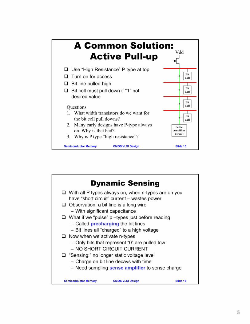
A Common Solution: Active Pull-up
Use “High Resistance” P type at top
Turn on for access
Bit line pulled high
Bit cell must pull down if “1” not desired value
Semiconductor Memory Slide 15
SenseAmplifier
Circuit
BitCell
BitCell
BitCell
BitCell
Vdd
Questions:1. What width transistors do we want for
the bit cell pull downs?2. Many early designs have P-type always
on. Why is that bad?3. Why is P type “high resistance”?
CMOS VLSI Design
Dynamic Sensing With all P types always on, when n-types are on you
have “short circuit” current – wastes power Observation: a bit line is a long wire
– With significant capacitance What if we “pulse” p –types just before reading
– Called precharging the bit lines– Bit lines all “charged” to a high voltage
Now when we activate n-types– Only bits that represent “0” are pulled low– NO SHORT CIRCUIT CURRENT
“Sensing:” no longer static voltage level– Charge on bit line decays with time– Need sampling sense amplifier to sense charge
Semiconductor Memory Slide 16
9
CMOS VLSI Design
Row and ColumnDecoders
Semiconductor Memory Slide 17
CMOS VLSI Design
Row Decoder: n bit address in, 2n rows out
WL [0]
BL [0]
WL [1]
WL [2]
WL [3]
VDD
BL [1]
Pull-up devices
BL [2] BL [3]
A1
A0
A1
A0
A1
A0
A1
A0
Semiconductor Memory Slide 18
10
CMOS VLSI Design
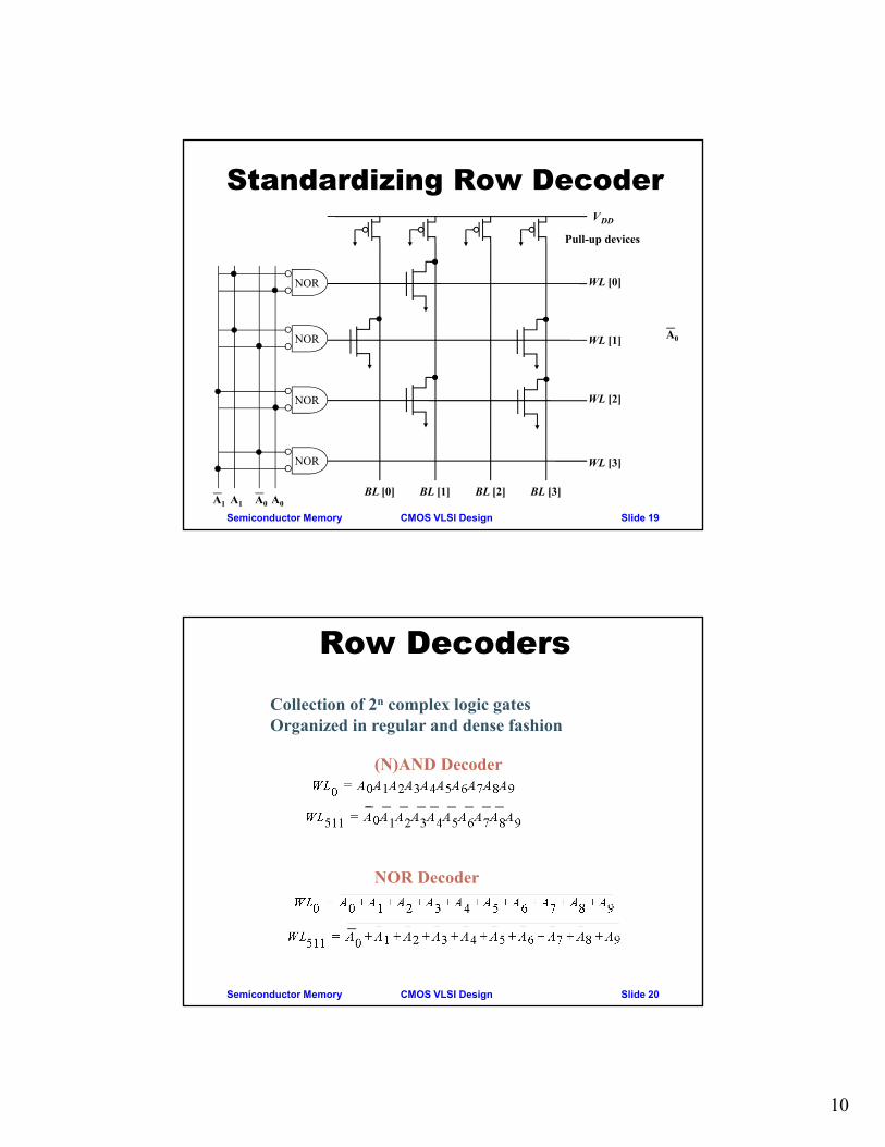
Standardizing Row Decoder
WL [0]
BL [0]
WL [1]
WL [2]
WL [3]
VDD
BL [1]
Pull-up devices
BL [2] BL [3]
NOR
A1
A0NOR
NOR
NOR
A1 A0 A0
Semiconductor Memory Slide 19
CMOS VLSI Design
Row Decoders
Collection of 2n complex logic gatesOrganized in regular and dense fashion
(N)AND Decoder
NOR Decoder
Semiconductor Memory Slide 20
11
CMOS VLSI Design
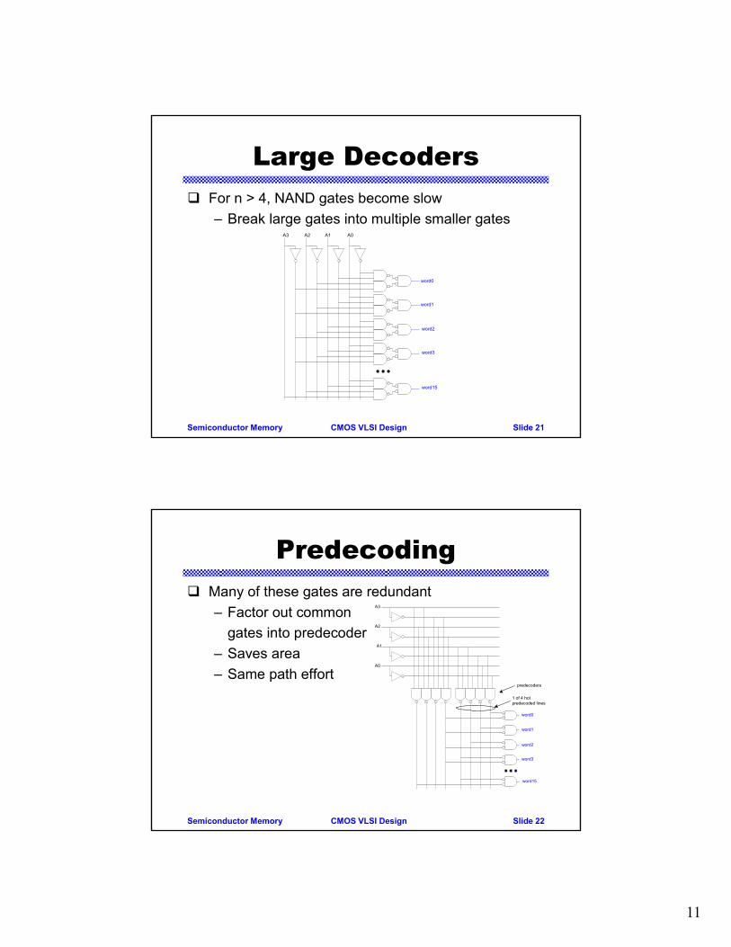
Large Decoders For n > 4, NAND gates become slow
– Break large gates into multiple smaller gates
word0
word1
word2
word3
word15
A0A1A2A3
Semiconductor Memory Slide 21
CMOS VLSI Design
Predecoding Many of these gates are redundant
– Factor out common
gates into predecoder
– Saves area
– Same path effortA0
A1
A2
A3
word1
word2
word3
word15
word0
1 of 4 hotpredecoded lines
predecoders
Semiconductor Memory Slide 22
12
CMOS VLSI Design
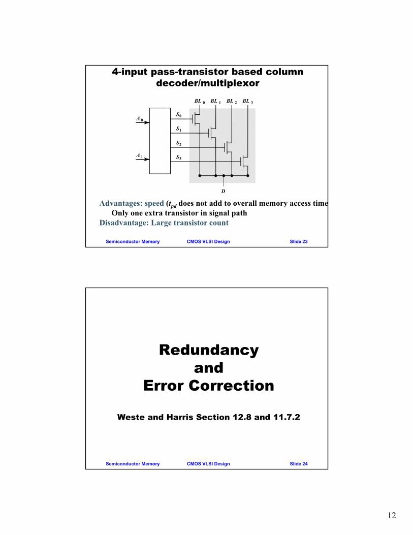
4-input pass-transistor based column decoder/multiplexor
Advantages: speed (tpd does not add to overall memory access time)Only one extra transistor in signal path
Disadvantage: Large transistor count
A 0S0
BL 0 BL 1 BL 2 BL 3
A 1
S1
S2
S3
D
Semiconductor Memory Slide 23
CMOS VLSI Design
Redundancyand
Error Correction
Weste and Harris Section 12.8 and 11.7.2
Semiconductor Memory Slide 24
13
CMOS VLSI Design
Redundancy To improve yield, large memory arrays typically have
redundant rows and columns.
During testing, defective bits, rows, and columns are identified.
Algorithm then determines which rows and/or columns to replace to avoid the defective bits.
Laser programming or fuses are used to program the replacements into the chip
Semiconductor Memory Slide 25
CMOS VLSI Design
Error Correction Large memory arrays can also have soft errors due to signals
being marginal.
– The larger the number of bits, the larger the distribution of signals.
– What is the error rate for a memory?
• 1 error in 1012 reads is not acceptable
• 1 error in 1016 reads is acceptable for most applications– A few errors per year at 1 GHz read rate.
• 1 error in 1024 reads is needed for applications in financial institutions
A 64 bit word plus nine parity bits (73 bits total) can be used to correct one bit error in the 64 bit word and detect two bit errors.
– The use of 64 bit single error correction would decrease the error rate from 1 error in 1012 to 1 error in 1016 reads.
Semiconductor Memory Slide 26
14
CMOS VLSI Design
SRAM: Static Random Access Memory
Weste and Harris
Section 12.2
Semiconductor Memory Slide 27
CMOS VLSI Design
Intel Nehalem I7 Processor
2008, 45 nm CMOS
SRAM used in registers, L1 and L2 Caches in Cores and Shared L3 Cache
90+% of chip is SRAMSemiconductor Memory Slide 28
15
CMOS VLSI DesignSemiconductor Memory Slide 29
CMOS VLSI Design
6-transistor CMOS SRAM Cell
WL
BL
VDD
M5M6
M4
M1
M2
M3
BL
QQ
VDD
GND
QQ
WL
BLBL
M1 M3
M4M2
M5 M6
There are 2 bit lines per column: True and ComplementSense Amp looks for “1-0” or “0-1”
Pass Transistors
Semiconductor Memory Slide 30
16
CMOS VLSI Design
SRAM Read Precharge both bitlines high
Then turn on wordline
One of the two bitlines will be pulled down by the cell
Ex: A = 0, A_b = 1
– bit discharges, bit_b stays high
– But A bumps up slightly
Read stability
– A must not flip
– N1 >> N2
bit bit_b
N1
N2P1
A
P2
N3
N4
A_b
word
0.0
0.5
1.0
1.5
0 100 200 300 400 500 600
time (ps)
word bit
A
A_b bit_b
Semiconductor Memory Slide 31
CMOS VLSI Design
SRAM Write Drive one bitline high, the other low
Then turn on wordline
Bitlines overpower cell with new value
Ex: A = 0, A_b = 1, bit = 1, bit_b = 0
– Force A_b low, then A rises high
Writability
– Must overpower feedback inverter
– N2 >> P1word
A
A_b
bit_b
0.5
1.0
1.5
bit bit_b
N1
N2P1
A
P2
N3
N4
A_b
word
Semiconductor Memory Slide 32
17
CMOS VLSI Design
SRAM Sizing High bitlines must not overpower inverters during
reads
But low bitlines must write new value into cell
bit bit_b
med
A
weak
strong
med
A_b
word
Semiconductor Memory Slide 33
CMOS VLSI Design
SRAM Column ExampleRead Write
H H
SRAM Cell
word_q1
bit_v1f
bit_b_v1f
out_v1rout_b_v1r
1
2
word_q1
bit_v1f
out_v1r
2
MoreCells
Bitline Conditioning
2
MoreCells
SRAM Cell
word_q1
bit_v1f
bit_b_v1f
data_s1
write_q1
Bitline Conditioning
Semiconductor Memory Slide 34
18
CMOS VLSI Design
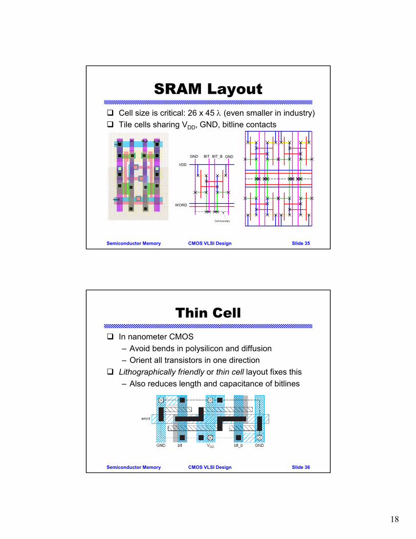
SRAM Layout Cell size is critical: 26 x 45 (even smaller in industry)
Tile cells sharing VDD, GND, bitline contacts
VDD
GND GNDBIT BIT_B
WORD
Cell boundary
Semiconductor Memory Slide 35
CMOS VLSI Design
Thin Cell In nanometer CMOS
– Avoid bends in polysilicon and diffusion
– Orient all transistors in one direction
Lithographically friendly or thin cell layout fixes this
– Also reduces length and capacitance of bitlines
Semiconductor Memory Slide 36
19
CMOS VLSI Design
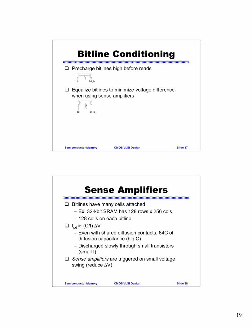
Bitline Conditioning Precharge bitlines high before reads
Equalize bitlines to minimize voltage difference when using sense amplifiers
bit bit_b
bit bit_b
Semiconductor Memory Slide 37
CMOS VLSI Design
Sense Amplifiers Bitlines have many cells attached
– Ex: 32-kbit SRAM has 128 rows x 256 cols
– 128 cells on each bitline
tpd (C/I) V
– Even with shared diffusion contacts, 64C of diffusion capacitance (big C)
– Discharged slowly through small transistors (small I)
Sense amplifiers are triggered on small voltage swing (reduce V)
Semiconductor Memory Slide 38
20
CMOS VLSI Design
Differential Pair Amp Differential pair requires no clock
But always dissipates static power
bit bit_bsense_b sense
N1 N2
N3
P1 P2
Semiconductor Memory Slide 39
CMOS VLSI Design
Clocked Sense Amp Clocked sense amp saves power
Requires sense_clk after enough bitline swing
Isolation transistors cut off large bitline capacitance
bit_bbit
sense sense_b
sense_clk isolationtransistors
regenerativefeedback
Semiconductor Memory Slide 40
21
CMOS VLSI Design
Decoder Layout Decoders must be pitch-matched to SRAM cell
Prototype ½ Gb DRAM for 3D Stackshttp://eda360insider.files.wordpress.com/2011/08/micron-hmc-memory-die-photo.jpg?w=571&h=442
256Mb DRAM
23
CMOS VLSI Design
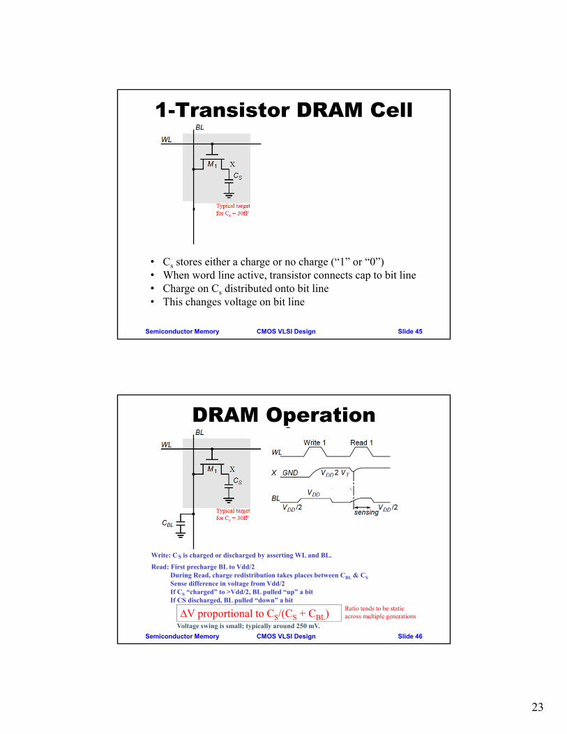
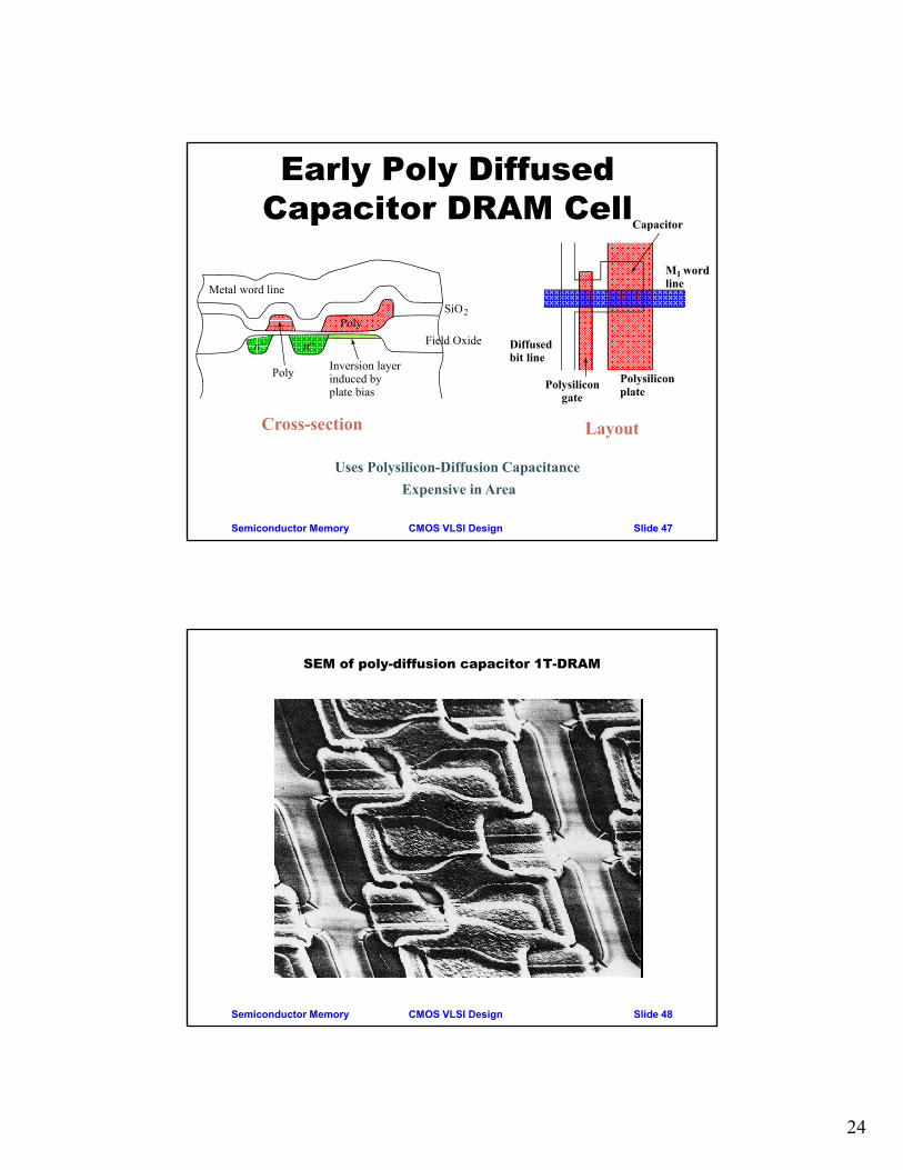
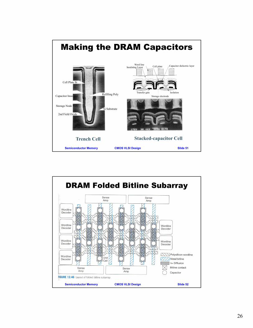
1-Transistor DRAM Cell
Semiconductor Memory Slide 45
• Cs stores either a charge or no charge (“1” or “0”)• When word line active, transistor connects cap to bit line• Charge on Cs distributed onto bit line• This changes voltage on bit line
CMOS VLSI Design
DRAM Operation
Semiconductor Memory Slide 46
Write: CS is charged or discharged by asserting WL and BL.
Read: First precharge BL to Vdd/2During Read, charge redistribution takes places between CBL & CS
Sense difference in voltage from Vdd/2If CS “charged” to >Vdd/2, BL pulled “up” a bitIf CS discharged, BL pulled “down” a bit
Voltage swing is small; typically around 250 mV.
Ratio tends to be staticacross multiple generations∆V proportional to CS/(CS + CBL)
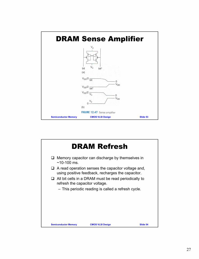
DRAM Refresh Memory capacitor can discharge by themselves in
~10-100 ms.
A read operation senses the capacitor voltage and, using positive feedback, recharges the capacitor.
All bit cells in a DRAM must be read periodically to refresh the capacitor voltage.
– This periodic reading is called a refresh cycle.
Semiconductor Memory Slide 54
28
CMOS VLSI Design
Flash Memory
Weste and Harris
Section 12.4.3
Semiconductor Memory Slide 55
CMOS VLSI Design
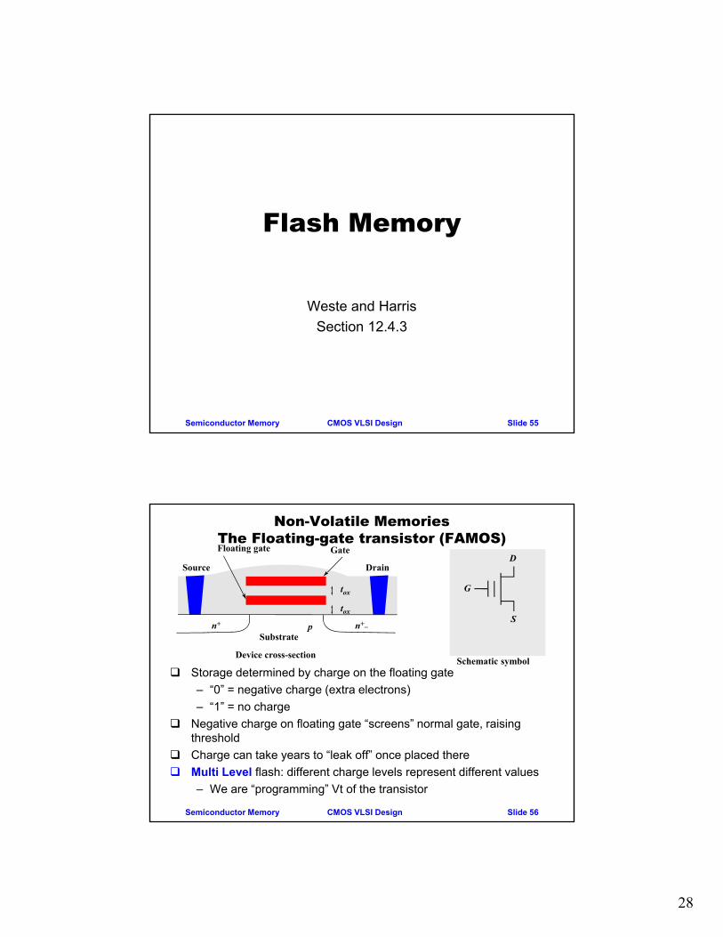
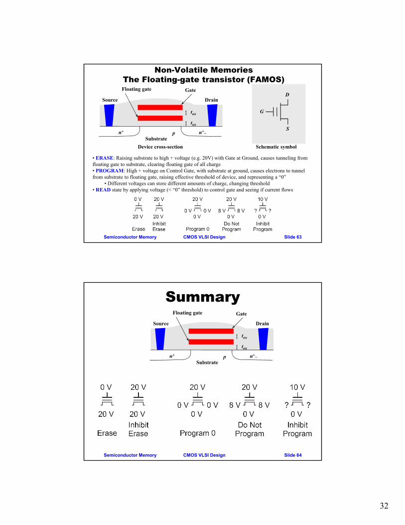
Non-Volatile Memories The Floating-gate transistor (FAMOS)
Storage determined by charge on the floating gate
– “0” = negative charge (extra electrons)
– “1” = no charge
Negative charge on floating gate “screens” normal gate, raising threshold
Charge can take years to “leak off” once placed there
Multi Level flash: different charge levels represent different values
– We are “programming” Vt of the transistor
Semiconductor Memory Slide 56
Floating gate
Source
Substrate
Gate
Drain
n+ n+_p
tox
tox
Device cross-sectionSchematic symbol
G
S
D
29
CMOS VLSI Design
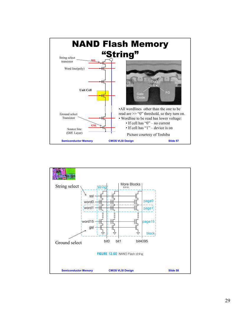
NAND Flash Memory “String”
Unit Cell
Word line(poly)
Source line(Diff. Layer) Picture courtesy of Toshiba
•All wordlines other than the one to be read are >> “0” threshold, so they turn on.• Wordline to be read has lower voltage:
• If cell has “0” – no current• If cell has “1” – device is on
Semiconductor Memory Slide 57
String selecttransistor
Ground selectTransistor
SSL
GSL
Gate
ONO
FGGateOxide
CMOS VLSI DesignSemiconductor Memory Slide 58
String select
Ground select
30
CMOS VLSI Design
NAND Flash MemoryWord linesSelect transistor
Bit line contact Source line contact
Active area
STI
Courtesy Toshiba
64 Gb (8GB) flash• 2 independent panes• 64K columns/pane• Thus 64kbit page• Each cell holds 4 bits• Each string = 64 cells• Each block has 256 pages• Each pane has 2K blocks
Semiconductor Memory Slide 59
CMOS VLSI Design
Reading Data Precharge bit lines
SSL & GSL set high
Set all word lines but desired page to high enough to turn transistors on, regardless of state
Set word line for desired page high enough to turn on IF NO CHARGE (“1”) is present on floating gate
Result depends on floating gate:
– If no charge (1), all transistors on & bit line discharged
– If negatively charged (0), bit line charge not disturbed
Semiconductor Memory Slide 60
Bit
lin
e
Word line
Question: Why do we have string select and ground select transistors?
SSL
GSL
31
CMOS VLSI Design
Programming (Writing) Data Cell “programmed” by placing electrons on floating
gate
Charge moved to/from via tunneling to substrate
Writing is done a page at a time
– Substrate held to ground
– Word line for selected page raised very high (e.g. 20V) to trigger tunneling
– Word line for all other pages at intermediate level (10V) guaranteed to turn transistors on, but not tunnel
– Desired bit values placed on bit lines
– If a “0” on bit line, then electrons tunnel to floating gate occurs
Semiconductor Memory Slide 61
Bit
lin
e
Word line
Note: we can ONLY PROGRAM ZEROs!!!
Selected page’sWord line
SSL
GSL
CMOS VLSI Design
Block Erasure
If we can only write “0”s, how do we store “1”s?
Answer: we “erase” all cells to 1 before writing and write only 0s
Erasing process:
– Set substrate very high (e.g. 20V)
– Set all control gates to ground
– Over time (ms), electrons on floating gates tunnel to substrate
Cannot control substrate voltage of single transistors, so erase allcells in a block at the same time
Semiconductor Memory Slide 62
Floating gate
Source
Substrate
Gate
Drain
n+ n+_p
tox
tox
20V
Gnd
Electron tunneling
32
CMOS VLSI Design
Non-Volatile Memories The Floating-gate transistor (FAMOS)Floating gate
Source
Substrate
Gate
Drain
n+ n+_p
tox
tox
Device cross-section Schematic symbol
G
S
D
• ERASE: Raising substrate to high + voltage (e.g. 20V) with Gate at Ground, causes tunneling from floating gate to substrate, clearing floating gate of all charge• PROGRAM: High + voltage on Control Gate, with substrate at ground, causes electrons to tunnel from substrate to floating gate, raising effective threshold of device, and representing a “0”
• Different voltages can store different amounts of charge, changing threshold• READ state by applying voltage (< “0” threshold) to control gate and seeing if current flows
Semiconductor Memory Slide 63
CMOS VLSI Design
Summary
Semiconductor Memory Slide 64
Floating gate
Source
Substrate
Gate
Drain
n+ n+_p
tox
tox
33
CMOS VLSI Design
Microcontrollers An example of SRAM combined with Flash Memory
Usually include many other functions
Semiconductor Memory Slide 65
CMOS VLSI Design
STM ARM Cortex-M3 MCU
Semiconductor Memory Slide 66
34
CMOS VLSI Design
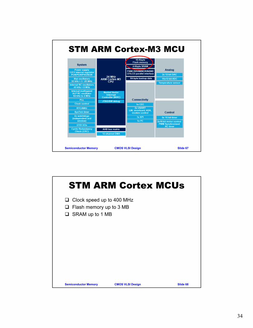
STM ARM Cortex-M3 MCU
Semiconductor Memory Slide 67
CMOS VLSI Design
STM ARM Cortex MCUs Clock speed up to 400 MHz
Flash memory up to 3 MB
SRAM up to 1 MB
Semiconductor Memory Slide 68
35
CMOS VLSI Design
Other Semiconductor Memory Technologies
Semiconductor Memory Slide 69
CMOS VLSI DesignJoe Nahas 28 Feb 2007Slide 70
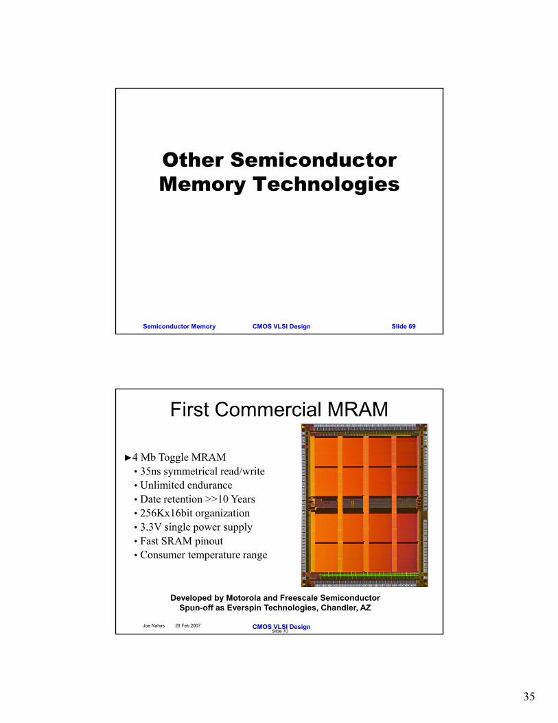
►4 Mb Toggle MRAM • 35ns symmetrical read/write• Unlimited endurance• Date retention >>10 Years• 256Kx16bit organization• 3.3V single power supply• Fast SRAM pinout• Consumer temperature range
First Commercial MRAM
Developed by Motorola and Freescale SemiconductorSpun-off as Everspin Technologies, Chandler, AZ
36
CMOS VLSI DesignJoe Nahas 28 Feb 2007Slide 71
MRAM Attributes Non-Volatility
– fast writing
– no write endurance limitation
Random Access
– no refresh
– no erase/program write sequence.
Non-destructive read
CMOS VLSI Design
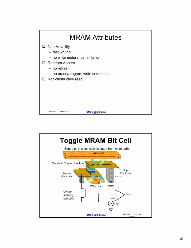
Toggle MRAM Bit Cell
Joe Nahas 28 Feb 2007Slide 72
Sense path electrically isolated from write path
ON for sensingselection
i Ref.
i sense
Write Line 1
Write Line 2
i
i
Bottom Electrode
Top Electrode
Magnetic Tunnel Junction
37
CMOS VLSI DesignJoe Nahas 28 Feb 2007Slide 73
Elements of Toggle Bit Balanced SAF free-layer Bit oriented 45º to lines Unipolar currents Overlapping pulse sequence Pre-read / decision write
WriteLine 1(H1)
WriteLine 2(H2)
HardAxis
EasyAxis
CMOS VLSI DesignJoe Nahas 28 Feb 2007Slide 74
HardAxisHardAxisHardAxis
EasyAxisEasyAxisEasyAxis
Write Line 2
Write Line 1
HardAxisHardAxisHardAxis
EasyAxisEasyAxisEasyAxis
Write Line 2
Write Line 1
HardAxisHardAxisHardAxis
EasyAxisEasyAxisEasyAxis
Write Line 2
HardAxisHardAxisHardAxis
EasyAxisEasyAxisEasyAxis
Write Line 2
HardAxisHardAxisHardAxis
EasyAxisEasyAxisEasyAxis
Write Line 2
Write Line 1
Write Line 1
Write Line 2
t0 t1 t2 t3 t4
Off
On
Off
On
H1
I 1
H2
I 2
H1
I 1
H2
I 2
WriteLine 1
Write Line 1
Toggle MRAM Switching Sequence
38
CMOS VLSI DesignJoe Nahas 28 Feb 2007Slide 75
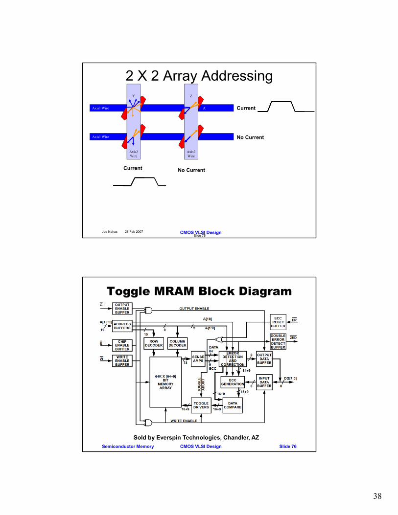
2 X 2 Array Addressing
Axis1 Wire A
Axis1 Wire
Y
Axis2 Wire
Z
Axis2 Wire
Current
No Current
Current No Current
CMOS VLSI DesignSemiconductor Memory Slide 76
Sold by Everspin Technologies, Chandler, AZ
Toggle MRAM Block Diagram
39
CMOS VLSI Design
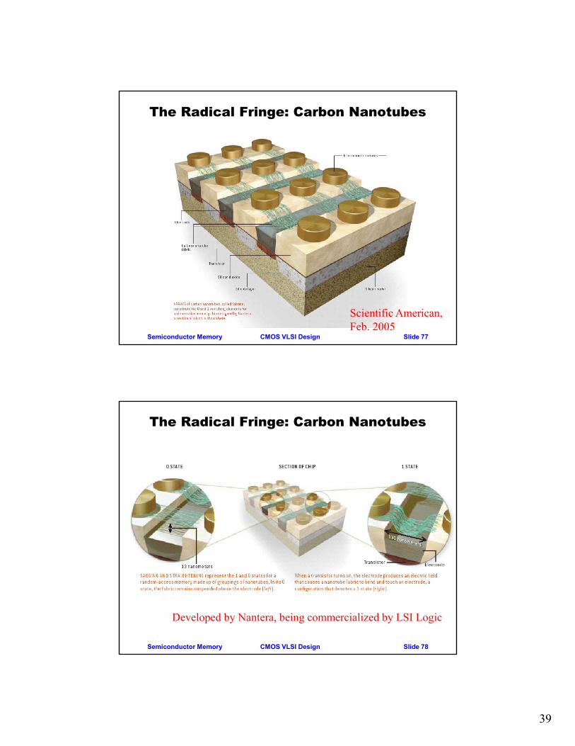
The Radical Fringe: Carbon Nanotubes
Scientific American,Feb. 2005
Semiconductor Memory Slide 77
CMOS VLSI Design
The Radical Fringe: Carbon Nanotubes
Developed by Nantera, being commercialized by LSI Logic